SL74LV245
System Logic
Semiconductor
SLS
OCTAL BUS TRANSCEIVER (3-State)
By pinning SL74LV245 are compatible with SL74HC245 and SL74HCT245 series. Input voltage levels
are compatible with standard CMOS levels.
∑
Output voltage levels are compatible with input levels of CMOS,
NMOS and TTL IC
S
∑
Supply voltage range: 2.0 to 3.2 V
∑
Low input current: 1.0
µ
¿; 0.1
µ
¿ at “ = 25
∞
—
∑
Output current 8 m¿
∑
Latch current value: not less 150 m¿ at “ = 125
∞
—
∑
ESD acceptable values: not less than 2000 V as per HBM and
not less 200 V as per ÃÃ
∑
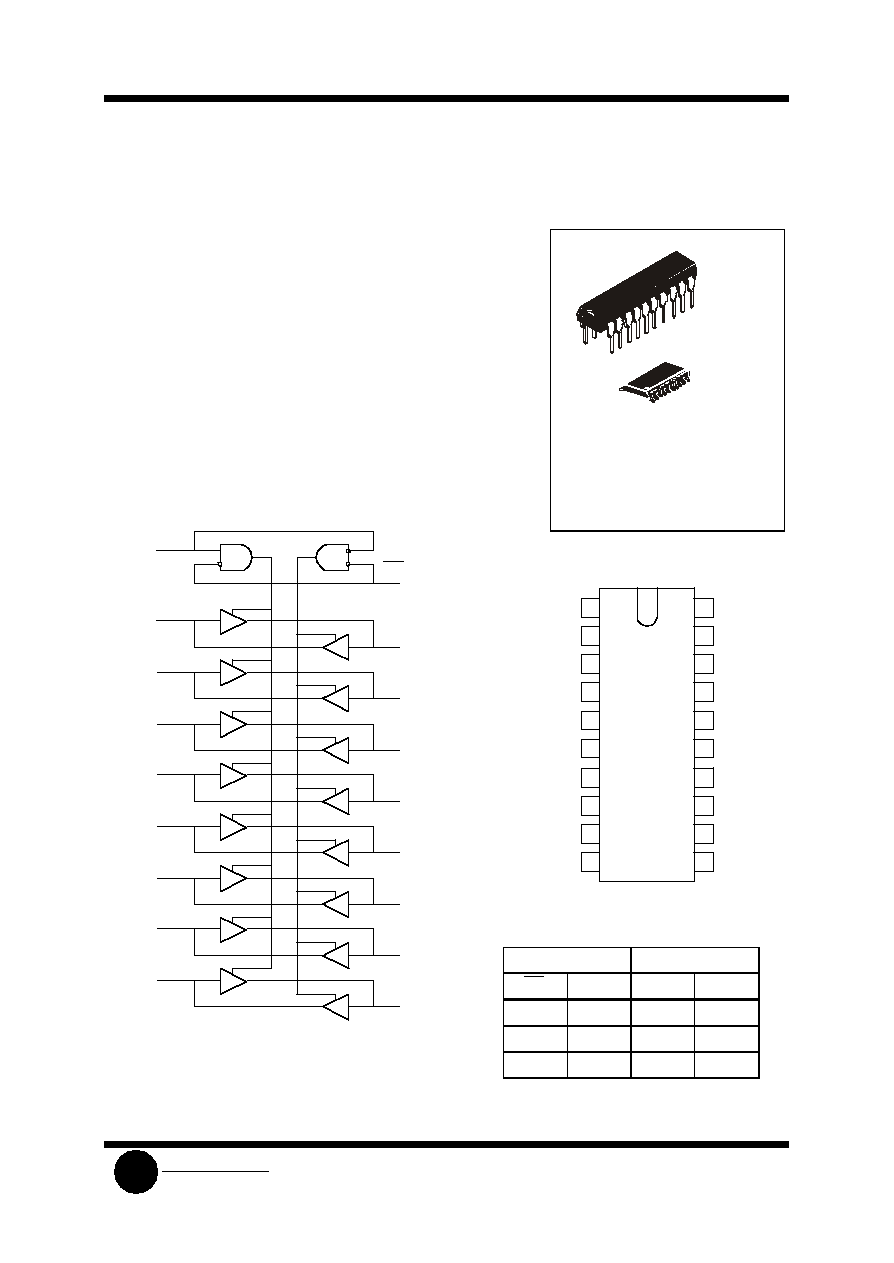
N SUFFIX
PLASTIC
D SUFFIX
SOIC
1
20
1
20
ORDERING INFORMATION
SL74LV245N Plastic DIP
SL74LV245D SOIC
T
A
= -40
∞
to 125
∞
C
for all packages
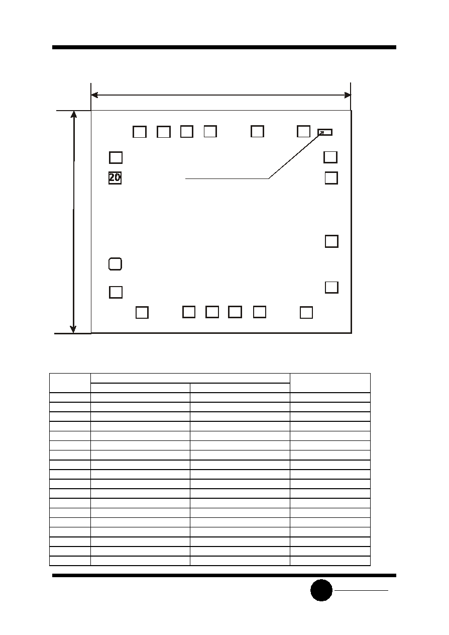
PIN ASSIGNMENT
245
DIR
01
A
0
02
A
1
03
A
2
04
A
3
05
A
4
06
A
5
07
A
6
08
A
7
09
GND
10
20
19
18
17
16
15
14
13
12
11
B
0
B
1
B
2
B
3
B
4
B
5
B
6
B
7
OE
V
CC
FUNCTION TABLE
Inputs
Inputs/Outputs
OE
DIR
¿
¬
L
L
A=B
input
L
H
input
B=A
H
X
Z
Z
BLOCK DIAGRAM
18
B
0
03
17
B
1
A
1
04
16
B
2
A
2
05
15
B
3
A
3
06
14
B
4
A
4
07
13
B
5
A
5
08
12
B
6
A
6
09
11
B
7
A
7
01
DIR
02
A
0
19
OE
Pin 20=V
CC
Pin 10 = GND
SL74LV245
System Logic
Semiconductor
SLS
ABSOLUTE MAXIMUM RATINGS*
Symbol
Parameter
Rating
Unit
V
CC
Supply voltage
-0.5 to +5.0
V
I
IK
*
1
Input diode current
±
20
m¿
I
OK
*
2
Output diode current
±
50
m¿
I
O
*
3
Output source or sink current
±
35
m¿
I
CC
V
CC
current
±
70
m¿
I
GND
GND current
±
70
m¿
P
D
Power dissipation per package:
Plastic DIP *
4
SOIC *
4
750
500
mW
Tstg
Storage temperature range
-65 to +150
∞
C
*
In absolute maximum ratings modes functioning is not guaranteed. Vpon lifting the absolute
maximum ratings functioning is guaranteed at the recommended operating conditions.
*
1
Provided V
I
< -0.5 V or V
I
> V
CC
+ 0.5 V.
*
2
Provided V
O
< -0.5 V or V
O
> V
CC
+ 0.5 V.
*
3
Provided -0.5 V < V
O
< V
CC
+ 0.5 V.
*
4
When operating in the temperature range of 70
∞
— to 125
∞
C power dissipation value decreases:
- for Plastic DIP by 1
2
mW/
∞
C
- for SOIC by
8
mW/
∞
C
RECOMMENDED OPERATING CONDITIONS
Symbol
Parameter
Min
Max
Unit
V
CC
Supply voltage
1.2
3.6
V
V
IN
Input voltage
0
V
CC
V
V
OUT
Output voltage
0
V
CC
V
T
A
Operating ambient temperature range. For all
package types
-40
125
∞
C
t
LH
, t
HL
Input rise and fall times
V
CC
=1.2 V
V
CC
=2.0 V
V
CC
=3.0 V
V
CC
=3.6 V
0
1000
700
500
400
ns