ChipFind - документация

Электронный компонент: SL74LV374N

Скачать:  PDF   ZIP
SL74LV374
System Logic
Semiconductor
SLS
OCTAL D-TIME FLIP-FLOP; POSITIVE EDGE-
TRIGGER (3-StatE)
SL74LV374 are compatible by pinning with SL74HC374 and
SL74HCT374 series. Input voltage levels are compatible with
standard CMOS levels.
Output voltage levels are compatible with input levels of CMOS,
NMOS and TTL IC
S
.
Supply voltage range from 2.0 to 3.2 V
LOW input current: 1.0
; 0.1
at = 25
Output current 8 m
Latch current value not less than 150 m at = 125
ESD acceptable values: not less than 2000 V as per HBM,
and not less than 200 V as per MM
ORDERING INFORMATION
SL74LV374N Plastic DIP
SL74LV374D SOIC
T
A
= -40
to 125
C
for all packages
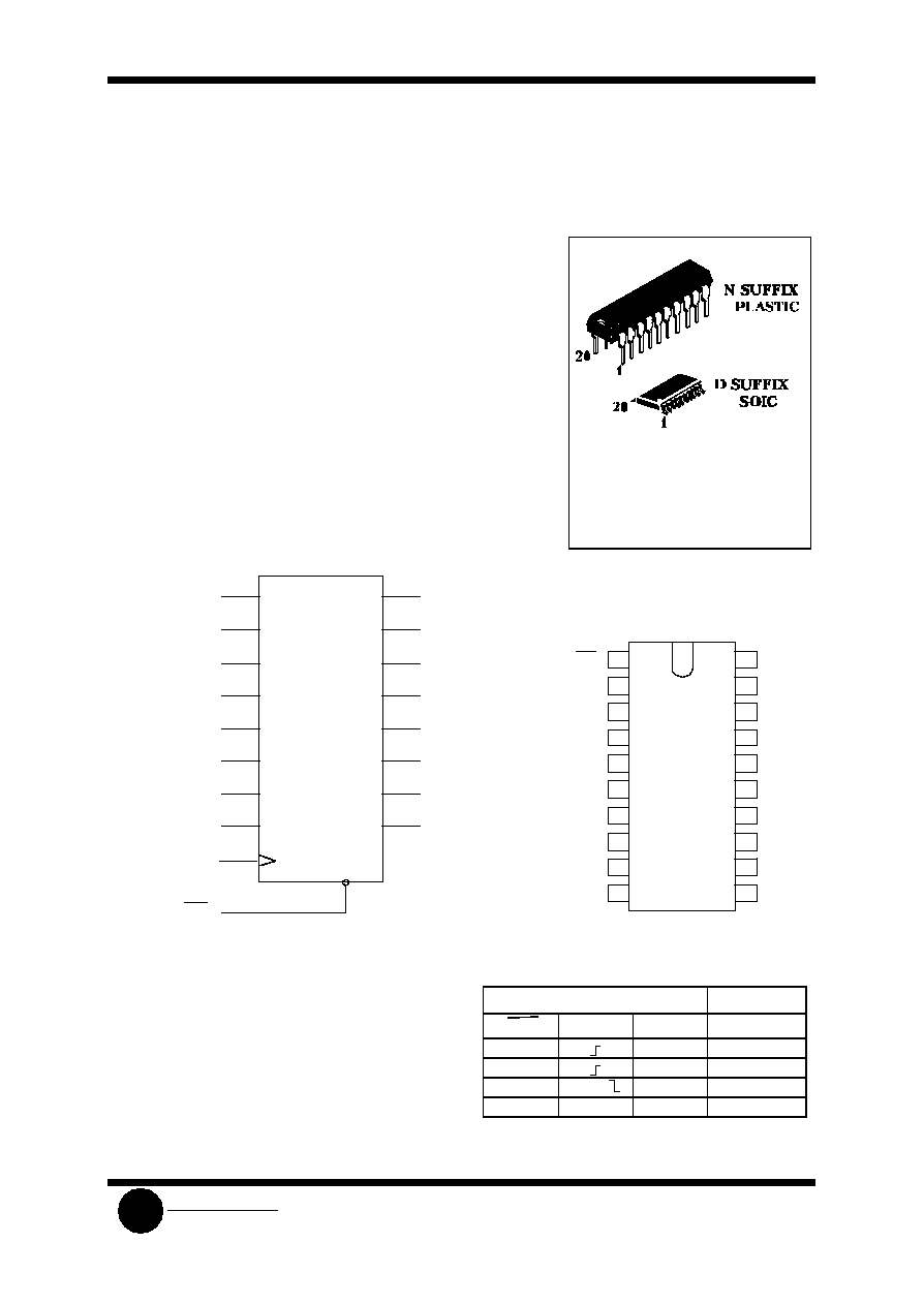
PIN ASSIGNMENT
374
OE
01
Q
0
02
D
0
03
D
1
04
Q
1
05
Q
2
06
D
2
07
D
3
08
Q
3
09
GND
10
20
19
18
17
16
15
14
13
12
11
D
7
D
6
Q
6
Q
5
D
5
D
4
Q
4
CP
V
CC
Q
7
BLOCK DIAGRAM
OE
01
Q
0
02
D
0
03
D
1
04
Q
1
05
Q
2
06
D
2
07
D
3
08
Q
3
09
19
18
17
16
15
14
13
12
11
D
7
D
6
Q
6
Q
5
D
5
D
4
Q
4
CP
Q
7
Pin 20=V
CC
Pin 10 = GND
FUNCTION TABLE
Inputs
Output
OE
CP
Dn
Qn
L
H
H
L
L
L
L
L, H,
X
no change
H
X
X
Z
SL74LV374
System Logic
Semiconductor
SLS
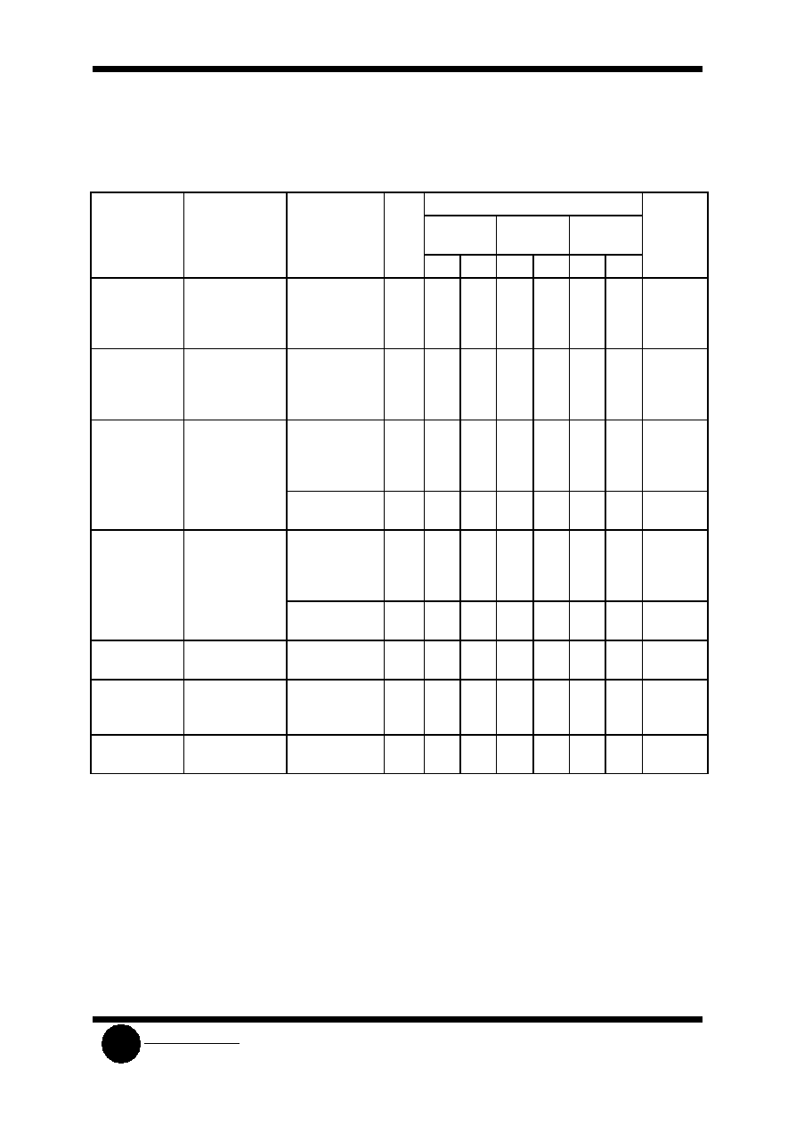
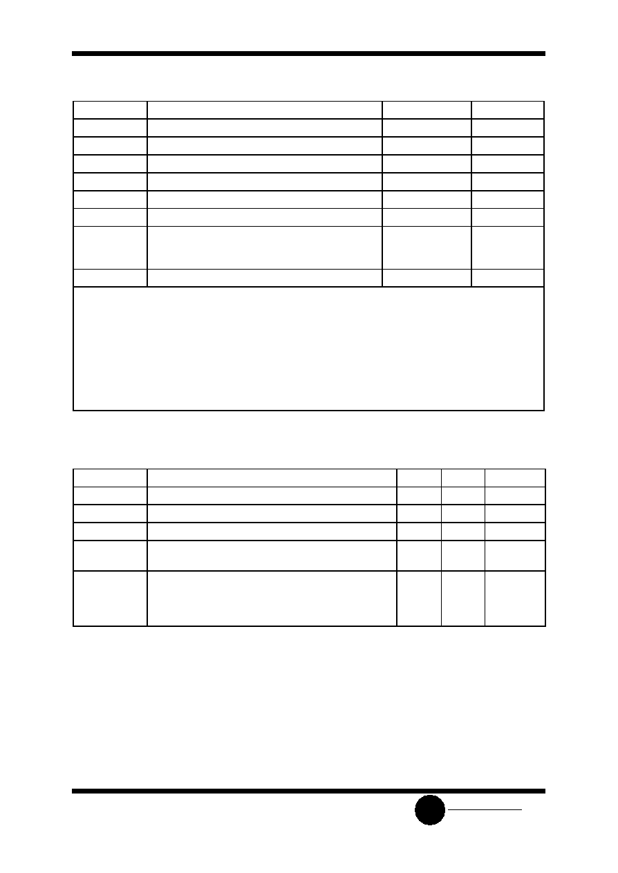
ABSOLUTE MAXIMUM RATINGS*
Symbol
Parameter
Rating
Unit
V
CC
Supply voltage
-0.5 to +5.0
V
I
IK
*
1
Input diode current
20
m
I
OK
*
2
Output diode current
50
m
I
O
*
3
Output source or sink current
35
m
I
CC
Bus driver outputs
70
m
I
GND
Ground current
70
m
P
D
Power dissipation per package,
Plastic DIP *
4
SOIC *
4
750
500
mW
Tstg
Storage temperature range
-65 to +150
C
*
In absolute maximum ratings modes functioning is not guaranteed. Upon lifting the absolute
maximum ratings functioning is guaranteed at the recommended operating conditions.
*
1
Provide V
I
< -0.5 V or V
I
> V
CC
+ 0.5 V.
*
2
Provide V
O
< -0.5 V or V
O
> V
CC
+ 0.5 V.
*
3
Provide -0.5 V < V
O
< V
CC
+ 0.5 V.
*
4
When operating in the temperature range of 70
C to 125
C power dissipation value decreases
- for Plastic DIP by 1
2
mW/
C
- for SOIC by
8
mW/
C
RECOMMENDED OPERATING MODES
Symbol
Parameter
Min
Max
Unit
V
CC
Supply voltage
1.2
3.6
V
V
IN
Input voltage
0
V
CC
V
V
OUT
Output voltage
0
V
CC
V
T
A
Operating ambient temperature range.
For all types packages
-40
125
C
t
LH
, t
HL
Input rise and fall times
V
CC
=1.2 V
V
CC
=2.0 V
V
CC
=3.0 V
V
CC
=3.6 V
0
1000
700
500
400
ns
SL74LV374
System Logic
Semiconductor
SLS
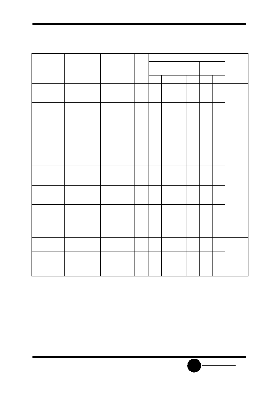
DC CHARACTERISTICS
Test
V
CC
,
Limits
Symbol
Parameter
coditions
V
25
C
-40
C to
85
C
125
C
Unit
min max
min
max
min
max
V
IH
HIGH level input
voltage
V
O
= V
CC
-0.1 V 1.2
2.0
3.0
3.6
0.9
1.4
2.1
2.5
-
-
-
-
0.9
1.4
2.1
2.5
-
-
-
-
0.9
1.4
2.1
2.5
-
-
-
-
V
V
IL
LOW level input
voltage
V
O
=0.1 V
1.2
2.0
3.0
3.6
-
-
-
-
0.3
0.6
0.9
1.1
-
-
-
-
0.3
0.6
0.9
1.1
-
-
-
-
0.3
0.6
0.9
1.1
V
V
OH
HIGH level
output voltage
V
I
= V
IH
or V
IL
I
O
= -50
1.2
2.0
3.0
3.6
1.1
1.92
2.92
3.52
-
-
-
-
1.
0
1.9
2.9
3.5
-
-
-
-
1.
0
1.9
2.9
3.5
-
-
-
-
V
V
I
= V
IH
or V
IL
I
O
= -8 m
3.0 2.48
-
2.34
-
2.20
-
V
V
OL
LOW level
output voltage
V
I
= V
IH
or V
IL
I
O
= 50
1.2
2.0
3.0
3.6
-
-
-
-
0.09
0.09
0.09
0.09
-
-
-
-
0.1
0.1
0.1
0.1
-
-
-
-
0.1
0.1
0.1
0.1
V
V
I
= V
IH
or V
IL
I
O
= 8 m
3.0
-
0.33
-
0.4
-
0.5
V
I
I
Input leakage
current
V
I
= V
CC
0 V
3.6
-
0.1
-
1.0
-
1.0
I
OZ
Output OFF-
state current
3-state outputs
V
I
= V
IL
or V
IH
V
O
=V
CC
or 0 V
3.6
-
0.5
-
5
-
10
I
CC
Suply current
V
I
=V
CC
or 0 V
I
O
= 0
3.6
-
8.0
-
80
-
160
SL74LV374
System Logic
Semiconductor
SLS
AC CHARACTERISTICS (C
L
=50 pF, t
LH
= t
HL
= 6.0 ns)
Test
V
CC
,
Limits
Symbol
Parameter
conditions
V
25
C
-40
C to
85
C
125
C
Unit
min max
min
max
min
max
t
PHL,
t
PLH
from CP to Qn
Propagation
delay
Figure 1
1.2
2.0
3.0
-
-
-
180
45
27
-
-
-
230
56
34
-
-
-
270
68
41
ns
t
PHZ
t
PLZ
from OE to Qn
Propagation
delay
Figure 3
1.2
2.0
3.0
-
-
-
160
38
25
-
-
-
200
57
36
-
-
-
240
68
43
t
PZH
t
PZL
from OE to Qn
Propagation
delay
Figure 3
1.2
2.0
3.0
-
-
-
160
38
23
-
-
-
200
48
29
-
-
-
240
58
35
t
THL,
t
TLH
HIGH-to-LOW
and LOW-to-
HIGH transition
time
Figure 1
1.2
2.0
3.0
-
-
-
75
16
10
-
-
-
100
20
13
-
-
-
120
24
15
t
W
Clock pulse
width HIGH or
LOW
Figure 1
1.2
2.0
3.0
250
18
11
-
-
-
350
23
14
-
-
-
540
28
17
-
-
-
t
SU
Set-up time Dn
to CP
Figure 2
1.2
2.0
3.0
45
13
8
-
-
-
50
17
10
-
-
-
100
20
12
-
-
-
t
H
Hold time Dn to
CP
Figure 2
1.2
2.0
3.0
25
5
5
-
-
-
25
5
5
-
-
-
25
5
5
-
-
-
fc
CP naximum
pulse frequency
Figure 1
2.0
3.0
-
-
27
46
-
-
22
37
-
-
18
31
MHz
C
I
Input
capacitance
3.0
-
7
-
-
-
-
pF
C
PD
Power
dissipation
capacitance (per
flip-flop)
V
I
= 0 V or V
CC
3.0
-
34
-
-
-
-
SL74LV374
System Logic
Semiconductor
SLS
0.9
V
1
0.1
0.9
V
1
0.1
0.9
V
1
0.1
t
LH
t
PHL
t
PLH
t
TLH
t
THL
V
CC
GND
CP
V
1
= 0.5V
CC
Qn
V
1
0 B
V
1
t
W
1/fc
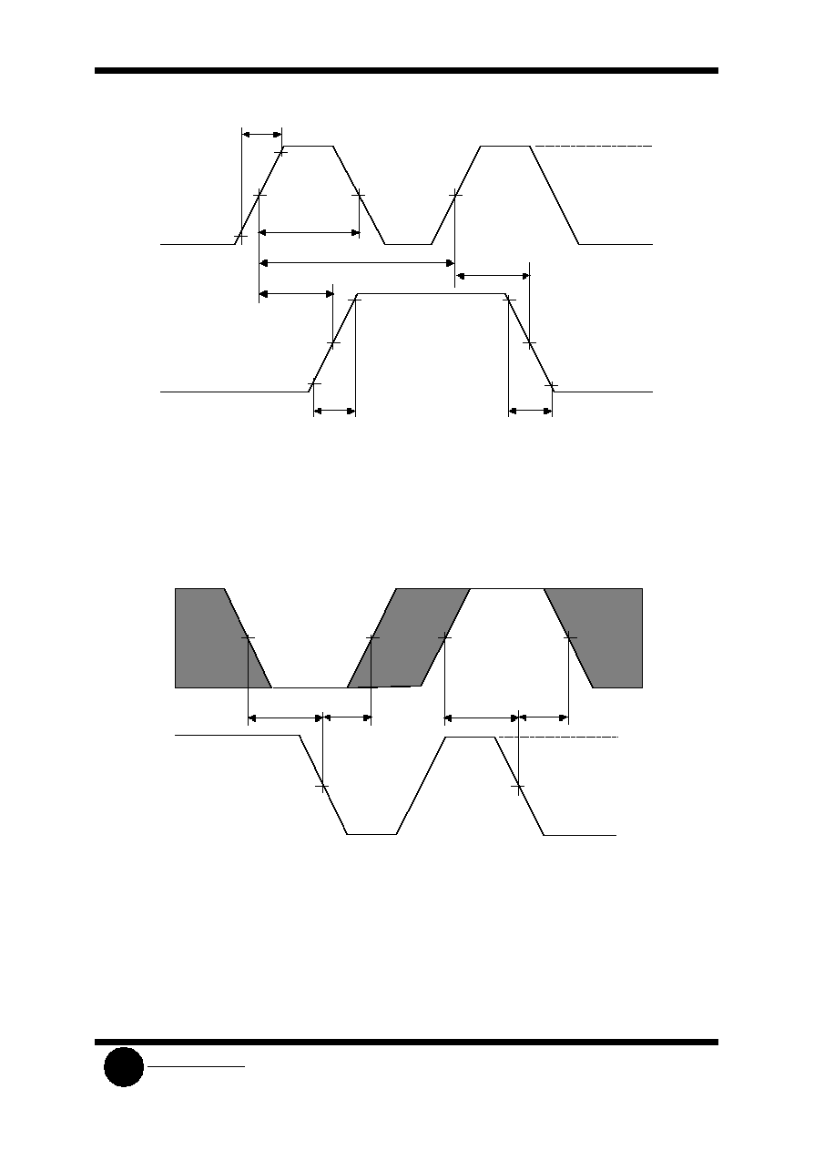
Figure 1- Time diagram
V
1
V
CC
GND
CP
V
1
V
1
V
1
V
1
V
1
t
SU
t
SU
t
H
t
H
Dn
V
CC
GND
V
1
= 0.5V
CC
Figure 2 - Time diagram
V