
SMSC DS ≠ LAN91C100FD REV. B
Rev. 05/31/2000
LAN91C100FD REV. B
PRELIMINARY
FEAST Fast Ethernet Controller
with Full Duplex Capability
FEATURES
Dual Speed CSMA/CD Engine (10 Mbps and 100
Mbps)
Compliant with IEEE 802.3 100BASE-T
Specification
Supports 100BASE-TX, 100BASE-T4, and
10BASE-T Physical Interfaces
32 Bit Wide Data Path (into Packet Buffer Memory)
Support for 32 and 16 Bit Buses
Support for 32, 16 and 8 Bit CPU Accesses
Synchronous, Asynchronous and Burst DMA
Interface Mode Options
128 Kbyte External Memory
Built-in Transparent Arbitration for Slave Sequential
Access Architecture
Early TX, Early RX Functions
Flat MMU Architecture with Symmetric Transmit
and Receive Structures and Queues
MII (Media Independent Interface) Compliant MAC-
PHY Interface Running at Nibble Rate
MII Management Serial Interface
Seven Wire Interface to 10 Mbps ENDEC
EEPROM-Based Setup
Full Duplex Capability
GENERAL DESCRIPTION
The LAN91C100FD is designed to facilitate the implementation of first generation Fast Ethernet adapters and connectivity
products. For this first generation of products, flexibility dominates over integration. The LAN91C100FD is a digital device
that implements the MAC portion of the CSMA/CD protocol at 10 and 100 Mbps, and couples it with a lean and fast data
and control path system architecture to ensure the CPU to packet RAM data movement does not cause a bottleneck at 100
Mbps.
Total memory size is 128 Kbytes, equivalent to a total chip storage (transmit plus receive) of 64 outstanding packets. The
LAN91C100FD is software compatible with the LAN9000 family of products and can use existing LAN9000 drivers (ODI,
IPX, and NDIS) in 16 and 32 bit Intel X86 based environments.
Memory management is handled using a unique MMU (Memory Management Unit) architecture and a 32-bit wide
data path. This I/O mapped architecture can sustain back-to-back frame transmission and reception for superior data
throughput and optimal performance. It also dynamically allocates buffer memory in an efficient buffer utilization
scheme, reducing software tasks and relieving the host CPU from performing these housekeeping functions. The
total memory size is 128 Kbytes (external), equivalent to a total chip storage (transmit and receive) of 64 outstanding
packets.
FEAST provides a flexible slave interface for easy connectivity with industry-standard buses. The Bus Interface Unit
(BIU) can handle synchronous as well as asynchronous buses, with different signals being used for each one.
FEAST's bus interface supports synchronous buses like the VESA local bus, as well as burst mode DMA for EISA
environments. Asynchronous bus support for ISA is supported even though ISA cannot sustain 100 Mbps traffic.
Fast Ethernet could be adopted for ISA-based nodes on the basis of the aggregate traffic benefits.
Two different interfaces are supported on the network side. The first is a conventional seven wire ENDEC interface that
connects to the LAN83C694 for 10BASE-T and coax 10 Mbps Ethernet networks. The second interface follows the MII
(Media Independent Interface) specification draft standard, consisting of 4 bit wide data transfers at the nibble rate. This
interface is applicable to 10 Mbps or 100 Mbps networks. Three of the LAN91C100FD's pins are used to interface to the
two-line MII serial management protocol. Four I/O ports (one input and three output pins) are provided for LAN83C694
configuration.

SMSC DS ≠ LAN91C100FD REV. B
Page 2
Rev. 05/31/2000
The LAN91C100FD is based on the LAN91C100 FEAST, functional revision G modified to add full duplex capability. Also
added is a software-controlled option to allow collisions to discard receive packets. Previously, the LAN91C100 supported
a "Diagnostic Full Duplex" mode. Under this mode the transmit packet is looped internally and received by the MAC. This
mode was enabled using the FDUPLX bit in the TCR. In order to avoid confusion, the new, broader full duplex function of
the LAN91C100FD is designated as Switched Full Duplex, and the TCR bit enabling it is designated as SWFDUP. When
the LAN91C100FD is configured for SWFDUP, its transmit and receive paths will operate independently and some
CSMA/CD functions will be disabled. When the controller is not configured for SWFDUP it will follow the CSMA/CD
protocol.
80 Arkay Drive
Hauppauge, NY 11788
(631)
435-6000
FAX (631) 273-3123
Copyright © SMSC 2004. All rights reserved.
Circuit diagrams and other information relating to SMSC products are included as a means of illustrating typical applications. Consequently, complete
information sufficient for construction purposes is not necessarily given. Although the information has been checked and is believed to be accurate, no
responsibility is assumed for inaccuracies. SMSC reserves the right to make changes to specifications and product descriptions at any time without
notice. Contact your local SMSC sales office to obtain the latest specifications before placing your product order. The provision of this information
does not convey to the purchaser of the described semiconductor devices any licenses under any patent rights or other intellectual property rights of
SMSC or others. All sales are expressly conditional on your agreement to the terms and conditions of the most recently dated version of SMSC's
standard Terms of Sale Agreement dated before the date of your order (the "Terms of Sale Agreement"). The product may contain design defects or
errors known as anomalies which may cause the product's functions to deviate from published specifications. Anomaly sheets are available upon
request. SMSC products are not designed, intended, authorized or warranted for use in any life support or other application where product failure
could cause or contribute to personal injury or severe property damage. Any and all such uses without prior written approval of an Officer of SMSC
and further testing and/or modification will be fully at the risk of the customer. Copies of this document or other SMSC literature, as well as the Terms
of Sale Agreement, may be obtained by visiting SMSC's website at http://www.smsc.com. SMSC is a registered trademark of Standard Microsystems
Corporation ("SMSC"). Product names and company names are the trademarks of their respective holders.
SMSC DISCLAIMS AND EXCLUDES ANY AND ALL WARRANTIES, INCLUDING WITHOUT LIMITATION ANY AND ALL IMPLIED WARRANTIES
OF MERCHANTABILITY, FITNESS FOR A PARTICULAR PURPOSE, TITLE, AND AGAINST INFRINGEMENT AND THE LIKE, AND ANY AND
ALL WARRANTIES ARISING FROM ANY COURSE OF DEALING OR USAGE OF TRADE.
IN NO EVENT SHALL SMSC BE LIABLE FOR ANY DIRECT, INCIDENTAL, INDIRECT, SPECIAL, PUNITIVE, OR CONSEQUENTIAL DAMAGES;
OR FOR LOST DATA, PROFITS, SAVINGS OR REVENUES OF ANY KIND; REGARDLESS OF THE FORM OF ACTION, WHETHER BASED ON
CONTRACT; TORT; NEGLIGENCE OF SMSC OR OTHERS; STRICT LIABILITY; BREACH OF WARRANTY; OR OTHERWISE; WHETHER OR
NOT ANY REMEDY OF BUYER IS HELD TO HAVE FAILED OF ITS ESSENTIAL PURPOSE, AND WHETHER OR NOT SMSC HAS BEEN
ADVISED OF THE POSSIBILITY OF SUCH DAMAGES.
ORDERING INFORMATION
Order Numbers:
LAN91C100FDQFP (208 Pin QFP Package)
LAN91C100FDTQFP (208 Pin TQFP Package)

SMSC DS ≠ LAN91C100FD REV. B
Page 3
Rev. 05/31/2000
TABLE OF CONTENTS
FEATURES................................................................................................................................1
GENERAL DESCRIPTION........................................................................................................1
PIN CONFIGURATION..............................................................................................................4
DESCRIPTION OF PIN FUNCTIONS .......................................................................................5
FUNCTIONAL DESCRIPTION ................................................................................................12
DATA STRUCTURES AND REGISTERS...............................................................................16
BOARD SETUP INFORMATION ............................................................................................46
APPLICATION CONSIDERATIONS.......................................................................................48
OPERATIONAL DESCRIPTION .............................................................................................56
MAXIMUM GUARANTEED RATINGS* ...................................................................................56
DC ELECTRICAL CHARACTERISTICS .................................................................................56
TIMING DIAGRAMS ................................................................................................................59
LAN91C100FD REV. B REVISIONS
...........................................................................68

SMSC DS ≠ LAN91C100FD REV. B
Page 4
Rev. 05/31/2000
PIN CONFIGURATION
LNK
TXEN
XTAL1
XTAL2
VDD
MIISEL
nCSOUT
nRXDISC
TX25
VDD
RX_ER
RX_DV
IOS0
GND
IOS1
IOS2
RX25
COL100
CRS100
RXD0
RXD1
RXD2
VDD
RXD3
TXD0
TXD1
VDD
TXD2
TXD3
TXEN100
nRWE0
GND
RD7
RD6
RD5
RD4
RDMAH
RD3
RD2
RD1
VDD
RD0
RD15
RD14
RD13
GND
RD12
RD11
RD10
GND
ENEEP
EEDO
1
2
3
4
5
6
7
8
9
10
11
12
13
14
15
16
17
18
19
20
21
22
23
24
25
26
27
28
29
30
31
32
33
34
35
36
37
38
39
40
41
42
43
44
45
46
47
48
49
50
51
52
A12
A11
A10
A9
A8
A7
A6
A5
A4
A3
A2
A1
D8
VDD
D9
D10
D11
D12
GND
D13
D14
D15
GND
D16
VDD
D17
D18
D19
GND
D20
D21
VDD
D22
D23
GND
D24
GND
VDD
D25
D26
GND
D27
D28
D29
D30
GND
D31
nRDYRTN
nLDEV
VDD
nSRDY
LCLK
156
155
154
153
152
151
150
149
148
147
146
145
144
143
142
141
140
139
138
137
136
135
134
133
132
131
130
129
128
127
126
125
124
123
122
121
120
119
118
117
116
115
114
113
112
111
110
109
108
107
106
105
CRS
CO
L
RX
D
AV
D
D
NC
AG
N
D
LB
K
TX
D
GN
D
RX
C
MD
I
TX
C
MD
O
nFSTEP
AU
I
S
E
L
AE
N
MC
L
K
VD
D
nD
A
T
A
C
S
IN
T
R
3
IN
T
R
2
IN
T
R
1
VD
D
GN
D
W/
nR
nC
Y
C
L
E
RE
S
E
T
nV
LBU
S
GN
D
VD
D
nWR
nR
D
IN
T
R
0
AR
D
Y
GN
D
D0
D1
D2
D3
GN
D
D4
D5
D6
VD
D
D7
nBE3
nB
E
2
nB
E1
nB
E0
A15
A1
4
A1
3
20
8
20
7
20
6
20
5
20
4
20
3
20
2
20
1
20
0
19
9
198
19
7
19
6
19
5
194
19
3
19
2
19
1
19
0
18
9
18
8
18
7
18
6
18
5
18
4
18
3
18
2
18
1
18
0
17
9
17
8
17
7
17
6
17
5
17
4
17
3
17
2
17
1
17
0
16
9
16
8
167
16
6
16
5
16
4
16
3
16
2
16
1
16
0
15
9
15
8
15
7
LAN91C100FD
208 Pin PQFP
and TQFP
53
54
55
56
57
58
59
60
61
62
63
64
65
66
67
68
69
70
71
72
73
74
75
76
77
78
79
80
81
82
83
84
85
86
87
88
89
90
91
92
93
94
95
96
97
98
99
100
101
102
103
104
EEDI
EE
SK
EEC
S
RD9
nR
WE1
NC
RD
8
RD23
RD
2
2
RD
2
1
VD
D
RD
20
RD
1
9
GN
D
RD
18
RD17
RD
1
6
RD
31
RD
30
NC
nR
WE2
VD
D
GN
D
RD2
9
RD
2
8
RD
27
RD
26
RD25
RD
2
4
GN
D
VD
D
RA
2
VD
D
nR
WE
3
RA3
RA4
RA
1
2
RA
5
RA6
RA13
RC
V
D
MA
GN
D
nADS
RA
7
nR
O
E
RA
11
RA8
RA
1
0
RA
9
RA
15
RA1
4
RA
1
6

SMSC DS ≠ LAN91C100FD REV. B
Page 5
Rev. 05/31/2000
DESCRIPTION OF PIN FUNCTIONS
PQFP/TQFP
PIN NO.
NAME
SYMBOL
BUFFER
TYPE
DESCRIPTION
148-159
Address
A4-A15
I
Input. Decoded by LAN91C100FD to determine
access to its registers.
145-147
Address
A1-A3
I
Input. Used by LAN91C100FD for internal register
selection.
193 Address
Enable
AEN
I
Input. Used as an address qualifier. Address
decoding is only enabled when AEN is low.
160-163 nByte
Enable
nBE0-
nBE3
I
Input. Used during LAN91C100FD register
accesses to determine the width of the access and
the register(s) being accessed. nBE0-nBE3 are
ignored when nDATACS is low (burst accesses)
because 32 bit transfers are assumed.
173-170,
168-166,
164, 144,
142-139,
137-135,
133,
131-129,
127, 126,
124, 123,
121, 118,
117,
115-112, 110
Data Bus
D0-D31
I/O24
Bidirectional. 32 bit data bus used to access the
LAN91C100FD's internal registers. Data bus has
weak internal pullups. Supports direct connection
to the system bus without external buffering. For
16 bit systems, only D0-D15 are used.
182
Reset
RESET
IS
Input. This input is not considered active unless it
is active for at least 100ns to filter narrow glitches.
95 nAddress
Strobe
nADS
IS
Input. For systems that require address latching,
the rising edge of nADS indicates the latching
moment for A1-A15 and AEN. All LAN91C100FD
internal functions of A1-A15, AEN are latched
except for nLDEV decoding.
183
nCycle
nCYCLE
I
Input. This active low signal is used to control
LAN91C100FD EISA burst mode synchronous bus
cycles.
184 Write/
nRead
W/nR
IS
Input. Defines the direction of synchronous cycles.
Write cycles when high, read cycles when low.
181 nVL
Bus
Access
nVLBUS I
with
pullup
Input. When low, the LAN91C100FD synchronous
bus interface is configured for VL Bus accesses.
Otherwise, the LAN91C100FD is configured for
EISA DMA burst accesses. Does not affect the
asynchronous bus interface.
105 Local
Bus
Clock
LCLK
I
Input. Used to interface synchronous buses.
Maximum frequency is 50 MHz. Limited to 8.33
MHz for EISA DMA burst mode.
175
Asynchron-
ous Ready
ARDY
OD16
Open drain output. ARDY may be used when
interfacing asynchronous buses to extend
accesses. Its rising (access completion) edge is
controlled by the XTAL1 clock and, therefore,
asynchronous to the host CPU or bus clock.
106 nSynchron
-
ous Ready
nSRDY
O16
Output. This output is used when interfacing
synchronous buses and nVLBUS=0 to extend
accesses. This signal remains normally inactive,
and its falling edge indicates completion. This
signal is synchronous to the bus clock LCLK.

SMSC DS ≠ LAN91C100FD REV. B
Page 6
Rev. 05/31/2000
DESCRIPTION OF PIN FUNCTIONS
PQFP/TQFP
PIN NO.
NAME
SYMBOL
BUFFER
TYPE
DESCRIPTION
109 nReady
Return
nRDYRTN
I
Input. This input is used to complete synchronous
read cycles. In EISA burst mode it is sampled on
falling LCLK edges, and synchronous cycles are
delayed until it is sampled high.
176,
187-189
Interrupt INTR0-
INTR3
O24
Outputs. Only one of these interrupts is selected to
be used; the other three are tri-stated. The
selection is determined by the value of INT SEL 1-
0 bits in the Configuration Register.
108 nLocal
Device
nLDEV
O16
Output. This active low output is asserted when
AEN is low and A4-A15 decode to the
LAN91C100FD address programmed into the high
byte of the Base Address Register. nLDEV is a
combinatorial decode of unlatched address and
AEN signals.
177 nRead
Strobe
nRD
IS
Input. Used in asynchronous bus interfaces.
178 nWrite
Strobe
nWR
IS
Input. Used in asynchronous bus interfaces.
190 nData
Path
Chip
Select
nDATACS I
with
pullup
Input. When nDATACS is low, the Data Path can
be accessed regardless of the values of AEN, A1-
A15 and the content of the BANK SELECT
Register. nDATACS provides an interface for
bursting to and from the LAN91C100FD 32 bits at
a time.
54 EEPROM
Clock
EESK
O4
Output. 4
µsec clock used to shift data in and out
of the serial EEPROM.
55 EEPROM
Select
EECS
O4
Output. Serial EEPROM chip select. Used for
selection and command framing of the serial
EEPROM.
52 EEPROM
Data Out
EEDO
O4
Output. Connected to the DI input of the serial
EEPROM.
53 EEPROM
Data In
EEDI I
with
pulldown
Input. Connected to the DO output of the serial
EEPROM.
13, 15, 16
I/O Base
IOS0-IOS2
I with
pullup
Input. External switches can be connected to these
lines to select between predefined EEPROM
configurations.
51 Enable
EEPROM
ENEEP I
with
pullup
Input. Enables (when high or open)
LAN91C100FD accesses to the serial EEPROM.
Must be grounded if no EEPROM is connected to
the LAN91C100FD.
42, 40-38,
36-33
RAM Data
Bus
RD0-RD7 I/O4
with
pullups
Bidirectional. Carries the local buffer memory read
and write data. Reads are always 32 bits wide.
Writes are controlled individually at the byte level.
Floated if FLTST=1 during RECEIVE FRAME
STATUS WORD writes for packet forwarding
information (RA2-RA16=0, RCVDMA=1, nRWE0-
nRWE3=0).
59, 56,
49-47,
45-43,
69-67, 65,
64, 62-60,
81-76, 71, 70
RAM Data
Bus
RD8-RD31 I/O4
with
pullups
Bidirectional. Carries the local buffer memory read
and write data. Reads are always 32 bits wide.
Writes are controlled individually at the byte level.

SMSC DS ≠ LAN91C100FD REV. B
Page 7
Rev. 05/31/2000
DESCRIPTION OF PIN FUNCTIONS
PQFP/TQFP
PIN NO.
NAME
SYMBOL
BUFFER
TYPE
DESCRIPTION
84, 87, 88,
90, 91, 96,
99, 101, 100,
98, 89, 92,
103, 102,
104
RAM
Address
Bus
RA2-RA16
O4
Outputs. This bus specifies the buffer RAM
doubleword being accessed by the
LAN91C100FD.
97
nROE
O4
Output. Active low signal used to read a
doubleword from buffer RAM.
31, 57, 73,
86
nRWE0-
RWE3
O4
Outputs. Active low signals used to write any byte,
word or dword in RAM.
93 Receive
DMA
RCVDMA
O4
Output. This pin is active during LAN91C100FD
write memory cycles of receive packets.
3
4
Crystal 1
Crystal 2
XTAL1
XTAL2
Iclk
An external 25 MHz crystal is connected across
these pins. If a TTL clock is supplied instead, it
should be connected to XTAL1 and XTAL2 should
be left open.
5, 10, 23, 27,
41, 63, 74,
83, 85, 107,
119, 125,
132, 143,
165, 179,
186, 191
Power
VDD
+5V power supply pins.
205 Analog
Power
AVDD
+5V analog power supply pins.
14, 32, 46,
50, 66, 75,
82, 94, 111,
116, 120,
122, 128,
134, 138,
169, 174,
180, 185,
200
Ground GND
Ground
pins.
203 Analog
Ground
AGND
Analog ground pin.
2 Transmit
Enable
TXEN
O4
Output. Used for 10 Mbps ENDEC. This pin stays
low when MIISEL is high.
201 Transmit
Data
TXD
O4
Output. NRZ Transmit Data for 10 Mbps ENDEC
interface.
208 Carrier
Sense
CRS I
with
pulldown
Input. Carrier sense from 10 Mbps ENDEC
interface. This pin is ignored when MIISEL is high.
207 Collision
Detect
COL I
with
pulldown
Input. Collision detection indication from 10 Mbps
ENDEC interface. This pin is ignored when
MIISEL is high.
206 Receive
Data
RXD I
with
pullup
Input. NRZ Receive Data from 10 Mbps ENDEC
interface. This pin is ignored when MIISEL is high.
197 Transmit
Clock
TXC I
with
pullup
Input. 10 MHz transmit clock used in 10 Mbps
operation. This pin is ignored when MIISEL is
high.
199 Receive
Clock
RXC I
with
pullup
Input. 10 MHz receive clock recovered by the 10
Mbps ENDEC. This pin is ignored when MIISEL is
high.

SMSC DS ≠ LAN91C100FD REV. B
Page 8
Rev. 05/31/2000
DESCRIPTION OF PIN FUNCTIONS
PQFP/TQFP
PIN NO.
NAME
SYMBOL
BUFFER
TYPE
DESCRIPTION
202
Loopback
LBK
O4
Output. Active when LOOP bit is set (TCR bit 1).
Independent of port selection (MIISEL=X).
1 nLink
Status
nLNK I
with
pullup
Input. General purpose input port used to convey
LINK status (EPHSR bit 14). Independent of port
selection (MIISEL=X).
195
nFullstep
nFSTEP
O4
Output. Non volatile output pin. Driven by inverse
of FULLSTEP (CONFIG bit 10). Independent of
port selection (MIISEL=X).
6 MII
Select
MIISEL O4
Output.
Non
volatile output pin. Driven by MII
SELECT (CONFIG bit 15). High indicates the MII
port is selected, low indicates the 10 Mbps ENDEC
is selected.
194
AUI Select AUISEL
O4
Output. Non volatile output pin. Driven by AUI
SELECT (CONFIG bit 8). Independent of port
selection (MIISEL= X).
30 Transmit
Enable
100 Mbps
TXEN100
O12
Output to MII PHY. Envelope to 100 Mbps
transmission. This pin stays low if MIISEL is low.
19 Carrier
Sense 100
Mbps
CRS100 I
with
pulldown
Input from MII PHY. Envelope of packet reception
used for deferral and backoff purposes. This pin is
ignored when MIISEL is low.
12 Receive
Data Valid
RX_DV I
with
pulldown
Input from MII PHY. Envelope of data valid
reception. Used for receive data framing. This pin
is ignored when MIISEL is low.
18 Collision
Detect 100
Mbps
COL100 I
with
pulldown
Input from MII PHY. Collision detection input. This
pin is ignored when MIISEL is low.
25, 26, 28,
29
Transmit
Data
TXD0-
TXD3
O12
Outputs. Transmit Data nibble to MII PHY.
9 Transmit
Clock
TX25 I
with
pullup
Input. Transmit clock input from MII. Nibble rate
clock (25 MHz). This pin is ignored when MIISEL
is low.
17 Receive
Clock
RX25 I
with
pullup
Input. Receive clock input from MII PHY. Nibble
rate clock. This pin is ignored when MIISEL is low.
20, 21, 22,
24
Receive
Data
RXD0-
RXD3
I
Inputs. Received Data nibble from MII PHY.
These pins are ignored when MIISEL is low.
198 Manage-
ment Data
Input
MDI I
with
pulldown
MII management data input.
196 Manage-
ment Data
Output
MDO
O4
MII management data output.
192 Manage-
ment Clock
MCLK
O4
MII management clock.
11 Receive
Error
RX_ER I
with
pulldown
Input. Indicates a code error detected by PHY.
Used by the LAN91C100FD to discard the packet
being received. The error indication reported for
this event is the same as a bad CRC (Receive
Status Word bit 13). This pin is ignored when
MIISEL is low.

SMSC DS ≠ LAN91C100FD REV. B
Page 9
Rev. 05/31/2000
DESCRIPTION OF PIN FUNCTIONS
PQFP/TQFP
PIN NO.
NAME
SYMBOL
BUFFER
TYPE
DESCRIPTION
7 nChip
Select
Output
nCSOUT
O4
Output. Chip Select provided for mapping of PHY
functions into LAN91C100FD decoded space.
Active on accesses to LAN91C100FD's eight lower
addresses when the BANK SELECTED is 7.
8 nReceive
Packet
Discard
nRXDISC I
with
pullup
Input. Used to discard the receive packet being
stored in memory. Assertion of the pin during a
packet reception results in the interruption of
packet reception into memory. The memory
allocated to the packet and the packet number in
use are freed. The input is driven asynchronously
and is synchronized internally by the
LAN91C100FD. Pin assertion may take place at
any time during the receive DMA packet. The
assertion has no effect if there is no packet being
DMAed to memory or if asserted during the last
DMA write to memory. Works for both MII and
ENDEC. The typical use of nRXDISC is with the
LAN91C100FD in PRMS mode with an external
associative memory use for address filtering.
*Note: The pin must be asserted for a minimum
of 80ns.
37
RDMAH
O4
Output. Active when the first dword of the address
is written (RCVDMA=1, RA10-RA4=0, RA3-
RA2=X).
Buffer Types
O4
Output buffer with 2mA source and 4mA sink
O12
Output buffer with 6mA source and 12mA sink
O16
Output buffer with 8mA source and 16mA sink
O24
Output buffer with 12mA source and 24mA sink
OD16
Open drain buffer with 16mA sink
I/O4
Bidirectional buffer with 2mA source and 4mA sink
I/O24
Bidirectional buffer with 12mA source and 24mA sink
I
Input buffer with TTL levels
IS
Input buffer with Schmitt Trigger Hysteresis
Iclk
Clock input buffer
DC levels and conditions defined in the DC Electrical Characteristics section.
SMSC DS ≠ LAN91C100FD REV. B
Page 10
Rev. 05/31/2000
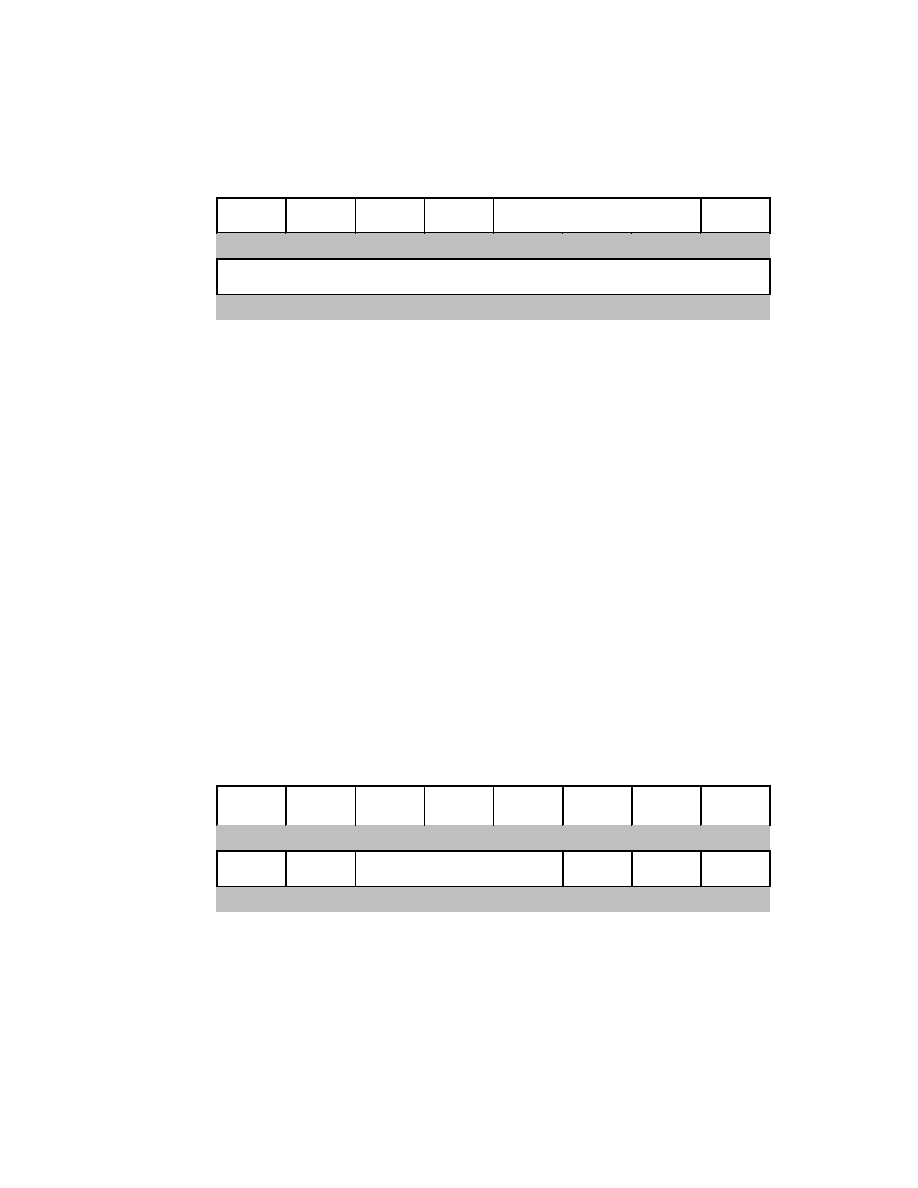
Table 1 - LAN91C100FD Pin Requirements
FUNCTION
PIN SYMBOLS
NUMBER OF PINS
System Address Bus
A1-A15, AEN, nBE0-nBE3
20
System Data Bus
D0-D31
32
System Control Bus
RESET, nADS, LCLK, ARDY,
nRDYRTN, nSRDY, INTR0-
INTR3, nLDEV, nRD, nWR,
nDATACS, nCYCLE, W/nR,
nVLBUS
17
Serial EEPROM
EEDI, EEDO, EECS, EESK,
ENEEP, IOS0-IOS2
8
RAM Data Bus
RD0-RD31
32
RAM Address Bus
RA2-RA16
15
RAM Control Bus
nROE, nRWE0-nRWE3,
RCVDMA, RDMAH
7
Crystal Oscillator
XTAL1, XTAL2
2
Power VDD,
AVDD
19
Ground GND,
AGND
21
External ENDEC 10 Mbps
TXEN, TXD, CRS, COL, RXD,
TXC, RXC, LBK, nLNK,
nFSTEP, AUISEL, MIISEL
12
Physical Interface 100 Mbps
TXEN100, CRS100, COL100,
RX_DV, RX_ER, TXD0-TXD3,
RXD0-RXD3, MDI, MDO, MCLK
16
Clocks TX25,
RX25
2
Miscellaneous nCSOUT,
nRXDISC
2
TOTAL
205
FIGURE 1 - LAN91C100FD BLOCK DIAGRAM
BUS
INTERFACE
UNIT
ARBITER
MEMORY
MANAGEMENT
UNIT
DIRECT
MEMORY
ACCESS
MEDIA
ACCESS
CONTROL
SERIAL
EEPROM
RD
FIFO
WR
FIFO
Address
Data
Control
RAM
25 MHz
10 Mb
Interface
100
Media
Independent
Interface
SMSC DS ≠ LAN91C100FD REV. B
Page 11
Rev. 05/31/2000
FIGURE 2 - LAN91C100FD SYSTEM DIAGRAM
ADDRESS
CONTROL
DATA
ADDRESS
CONTROL
DATA
SYSTEM BUS
SERIAL
EEPROM
1O Mbps
MII
RD0-31
OE,WE
RA
SRAM
32kx8
1
2
3 4
LAN91C100FD
FEAST
LAN83C69
10BASE-T
INTERFACE
10BASE-T
100BASE-T4
INTERFACE
CHIP
100BASE-T4
100BASE-TX
INTERFACE
LOGIC/
10BASE-T
100BASE-TX/
10BASE-T
OR

SMSC DS ≠ LAN91C100FD REV. B
Page 12
Rev. 05/31/2000
FUNCTIONAL DESCRIPTION
DESCRIPTION OF BLOCKS
Clock Generator Block
1) The XTAL1 and XTAL2 pins are to be connected to a 25 MHz crystal.
2) TXCLK and RXCLK are 10 MHz clock inputs. These clocks are generated by the external ENDEC in 10 Mbps mode
and are only used by the CSMA/CD block.
3) TX25 is an input clock. It will be the nibble rate of the particular PHY connected to the MII (2.5 MHz for a 10 Mbps
PHY, and 25 MHz for a 100 Mbps PHY).
4) RX25 - This is the MII nibble rate receive clock used for sampling received data nibbles and running the receive state
machine. (2.5 MHz for a 10 Mbps PHY, and 25 MHz for a 100 Mbps PHY).
5) LCLK - Bus clock - Used by the BIU for synchronous accesses. Maximum frequency is 50 MHz for VL BUS mode, and
8.33 MHz for EISA slave DMA.
CSMA/CD BLOCKCSMA/CD BLOCK
This is a 16 bit oriented block, with fully- independent Transmit and Receive logic. The data path in and out of the block
consists of two 16-bit wide uni-directional FIFOs interfacing the DMA block. The DMA port of the FIFO stores 32 bits to
exploit the 32 bit data path into memory, but the FIFOs themselves are 16 bit wide. The Control Path consists of a set of
registers interfaced to the CPU via the BIU.
DMA BlockDMA
This block accesses packet memory on the CSMA/CD's behalf, fetching transmit data and storing received data. It
interfaces the CSMA/CD Transmit and Receive FIFOs on one side, and the Arbiter block on the other. To increase the
bandwidth into memory, a 50 MHz clock is used by the DMA block, and the data path is 32 bits wide.
For example, during active reception at 100 Mbps, the CSMA/CD block will write a word into the Receive FIFO every
160ns. The DMA will read the FIFO and accumulate two words on the output port to request a memory cycle from the
Arbiter every 320ns.
DMA will discard a packet if nRXDISC is asserted for a minimum of 80ns during a reception. If asserted late, the DMA will
receive the packet normally. The nRXDISC is defined valid for the DMA interface for as long as the RCVDMA signal is
active.
The DMA machine is able to support full duplex operation. Independent receive and transmit counters are used. Transmit
and receive cycles are alternated when simultaneous receive and transmit accesses are needed.
Arbiter BlockARBITER
The Arbiter block sequences accesses to packet RAM requested by the BIU and by the DMA blocks. BIU requests
represent pipelined CPU accesses to the Data Register, while DMA requests represent CSMA/CD data movement. The
external memory used is a 25ns SRAM.
The Arbiter is also responsible for controlling the nRWE0-nRWE3 lines as a function of the bytes being written. Read
accesses are always 32 bit wide, and the Arbiter steers the appropriate byte(s) to the appropriate lanes as a function of the
address.
The CPU Data Path consists of two uni-directional FIFOs mapped at the Data Register location. These FIFOs can be
accessed in any combination of bytes, word, or doublewords. The Arbiter will indicate 'Not Ready' whenever a cycle is
initiated that cannot be satisfied by the present state of the FIFO.

SMSC DS ≠ LAN91C100FD REV. B
Page 13
Rev. 05/31/2000
MMU BlockMMU
The Hardware Memory Management Unit allocates memory and transmit and receive packet queues. It also determines
the value of the transmit and receive interrupts as a function of the queues. The page size is 2k, with a maximum memory
size of 128k. MIR and MCR values are interpreted in 512 byte units.
BIU BlockBIU
The Bus Interface Unit can handle synchronous as well as asynchronous buses; different signals are used for each one.
Transparent latches are added on the address path using rising nADS for latching.
When working with an asynchronous bus like ISA, the read and write operations are controlled by the edges of nRD and
nWR. ARDY is used for notifying the system that it should extend the access cycle. The leading edge of ARDY is
generated by the leading edge of nRD or nWR while the trailing edge of ARDY is controlled by the internal LAN91C100FD
clock and, therefore, asynchronous to the bus.
In the synchronous VL Bus type mode, nCYCLE and LCLK are used to for read and write operations. Completion of the
cycle may be determined by using nSRDY. nSRDY is controlled by LCLK and synchronous to the bus.
Direct 32 bit access to the Data Path is supported by using the nDATACS input. By asserting nDATACS, external DMA
type of devices will bypass the BIU address decoders and can sequentially access memory with no CPU intervention.
nDATACS accesses can be used in the EISA DMA burst mode (nVLBUS=1) or in asynchronous cycles. These cycles
MUST be 32 bit cycles. Please refer to the corresponding timing diagrams for details on these cycles.
The BIU is implemented using the following principles:
1) Address decoding is based on the values of A15-A4 and AEN.
2) Address latching is performed by using transparent latches that are transparent when nADS=0 and nRD=1, nWR=1
and latch on nADS rising edge.
3) Byte, word and doubleword accesses to all registers and Data Path are supported except a doubleword write to offset
Ch will only write the BANK SELECT REGISTER (offset Fh).
4) No bus byte swapping is implemented (no eight bit mode).
5) Word swapping as a function of A1 is implemented for 16 bit bus support.
6) The asynchronous interface uses nRD and nWR strobes. If necessary, ARDY is negated on the leading edge of the
strobe. The ARDY trailing edge is controlled by CLK.
7) The VLBUS synchronous interface uses LCLK, nADS, and W/nR as defined in the VESA specification as well as
nCYCLE to control read and write operations and generate nSRDY.
8) EISA burst DMA cycles to and from the DATA REGISTER are supported as defined in the EISA Slave Mode "C"
specification when nDATACS is driven by nDAK.
9) Synchronous and asynchronous cycles can be mixed as long as they are not active simultaneously.
10) Address and bank selection can be bypassed to generate 32 bit Data Path accesses by activating the nDATACS pin.
MAC-PHY Interface BlockMAC-PHY INTERFACE
Two separate interfaces are defined, one for the 10 Mbps bit rate interface and one for the MII 100 Mbps and 10 Mbps
nibble rate interface. The 10 Mbps ENDEC interface comprises the signals used for interfacing Ethernet ENDECs. The 100
Mbps interface follows the MII for 100 Mbps 802.3 networks proposal, and it is based on transferring nibbles between the
MAC and the PHY.
For the MII interface, transmit data is clocked out using the TX25 clock input, while receive data is clocked in using RX25.
In 100 Mbps mode, the LAN91C100FD provides the following interface signals to the PHY:

SMSC DS ≠ LAN91C100FD REV. B
Page 14
Rev. 05/31/2000
For transmission: TXEN100 TXD0-3 TX25
For reception: RX_DV RX_ER RXD0-3 RX25
For CSMA/CD state machines: CRS100 COL100
A transmission begins by TXEN100 going active (high), and TXD0-TXD3 having the first valid preamble nibble. TXD0
carries the least significant bit of the nibble (that is the one that would go first out of the EPH at 100 Mbps), while TXD3
carries the most significant bit of the nibble. TXEN100 and TXD0-TXD3 are clocked by the LAN91C100FD using TX25
rising edges. TXEN100 goes inactive at the end of the packet on the last nibble of the CRC.
During a transmission, COL100 might become active to indicate a collision. COL100 is asynchronous to the
LAN91C100FD's clocks and will be synchronized internally to TX25.
Reception begins when RX_DV (receive data valid) is asserted. A preamble pattern or flag octet will be present at RXD0-
RXD3 when RX_DV is activated. The LAN91C100FD requires no training sequence beyond a full flag octet for reception.
RX_DV as well as RXD0-RXD3 are sampled on RX25 rising edges. RXD0 carries the least significant bit and RXD3 the
most significant bit of the nibble. RX_DV goes inactive when the last valid nibble of the packet (CRC) is presented at
RXD0-RXD3.
RX_ER might be asserted during packet reception to signal the LAN91C100FD that the present receive packet is invalid.
The LAN91C100FD will discard the packet by treating it as a CRC error.
When MIISEL=1, RXD0-RXD3 should always be aligned to packet nibbles, therefore, opening flag detection does not
consider misaligned cases. Opening flag detection expects the 5Dh pattern and will not reject the packet on non-preamble
patterns. When MIISEL=0 the opening flag detection expects a "10101011" pattern and will use it for determining nibble
alignment.
CRS100 is used as a frame envelope signal for the CSMA/CD MAC state machines (deferal and backoff functions), but it is
not used for receive framing functions. CRS100 is an asynchronous signal and it will be active whenever there is activity on
the cable, including LAN91C100FD transmissions and collisions.
Switching between the ENDEC and MII interfaces is controlled by the MII SELECT bit in the CONFIG REGISTER. The
MIISEL pin reflects the value of this bit and may be used to control external multiplexing logic.
Note that given the modular nature of the MII, TX25 and RX25 cannot be assumed to be free running clocks. The
LAN91C100FD will not rely on the presence of TX25 and RX25 during reset and will use its own internal clock whenever a
timeout on TX25 is detected.
MII Management Interface Block
PHY management through the MII management interface is supported by the LAN91C100FD by providing the means to
drive a tri-statable data output, a clock, and reading an input. Timing and framing for each management command is to be
generated by the CPU.
Serial EEPROM Interface
This block is responsible for reading the serial EEPROM upon hardware reset (or equivalent command) and defining
defaults for some key registers. A write operation is also implemented by this block, that under CPU command will program
specific locations in the EEPROM. This block is an autonomous state machine and controls the internal Data Bus of the
LAN91C100FD during active operation.

SMSC DS ≠ LAN91C100FD REV. B
Page 15
Rev. 05/31/2000
FIGURE 3 - LAN91C100FD INTERNAL BLOCK DIAGRAM WITH DATA PATH
BUS INTERFACE
ARBITER
MMU
BUFFER RAM
CSMA/CD
DATA BUS
ADDRESS
BUS
CONTROL
EEPROM
EEPROM
WRITE
DATA
REG
READ
DATA
REG
TX
FIFO
TX
COMPL
FIFO
RX
FIFO
DMA
INTERFACE
ADDRESS
DATA
TRANSMIT
RECEIVE

SMSC DS ≠ LAN91C100FD REV. B
Page 16
Rev. 05/31/2000
DATA STRUCTURES AND REGISTERS
PACKET FORMAT IN BUFFER MEMORY
The packet format in memory is similar for the Transmit and Receive areas. The first word is reserved for the status word.
The next word is used to specify the total number of bytes, and it is followed by the data area. The data area holds the
packet itself.
FIGURE 4 - DATA PACKET FORMAT
TRANSMIT PACKET
RECEIVE PACKET
STATUS WORD
Written by CSMA upon transmit
completion (see Status Register)
Written by CSMA upon receive
completion (see RX Frame
Status Word)
BYTE COUNT
Written by CPU
Written by CSMA
DATA AREA
Written/modified by CPU
Written by CSMA
CONTROL BYTE
Written by CPU to control
odd/even data bytes
Written by CSMA; also has
odd/even bit
BYTE COUNT - Divided by two, it defines the total number of words including the STATUS WORD, the BYTE
COUNT WORD, the DATA AREA and the CONTROL BYTE.
The receive byte count always appears as even; the ODDFRM bit of the receive status word indicates if the low byte of the
last word is relevant.
The transmit byte count least significant bit will be assumed 0 by the controller regardless of the value written in memory.
DATA AREA - The data area starts at offset 4 of the packet structure and can extend up to 2043 bytes.
The data area contains six bytes of DESTINATION ADDRESS followed by six bytes of SOURCE ADDRESS, followed by a
variable-length number of bytes. On transmit, all bytes are provided by the CPU, including the source address. The
LAN91C100FD does not insert its own source address. On receive, all bytes are provided by the CSMA side.
bit15
bit0
RAM OFFSET
(decimal)
0
2
4
2046 max
STATUS WORD
reserved
BYTE
COUNT
DATA AREA
CONTROL BYTE
LAST DATA BYTE if odd
~~
~~
~~
~~
SMSC DS ≠ LAN91C100FD REV. B
Page 17
Rev. 05/31/2000
The 802.3 Frame Length word (Frame Type in Ethernet) is not interpreted by the LAN91C100FD. It is treated transparently
as data both for transmit and receive operations.
CONTROL BYTE - For transmit packets the CONTROL BYTE is written by the CPU as:
X X
ODD
CRC
0 0 0 0
ODD - If set, indicates an odd number of bytes, with the last byte being right before the CONTROL BYTE. If clear, the
number of data bytes is even and the byte before the CONTROL BYTE is not transmitted.
CRC - When set, CRC will be appended to the frame. This bit has only meaning if the NOCRC bit in the TCR is set.
For receive packets the CONTROL BYTE is written by the controller as:
0 1
ODD
0 0 0 0 0
ODD - If set, indicates an odd number of bytes, with the last byte being right before the CONTROL BYTE. If clear, the
number of data bytes is even and the byte before the CONTROL BYTE should be ignored.
RECEIVE FRAME STATUS WORDRECEIVE FRAME STATUS WORD
This word is written at the beginning of each receive frame in memory. It is not available as a register.
HIGH
BYTE
ALGN
ERR
BROD
CAST
BAD
CRC
ODD
FRM
TOOLNG
TOO
SHORT
LOW
BYTE
HASH
VALUE
MULT
CAST
5 4 3 2 1 0
ALGNERR - Frame had alignment error. When MII SEL=1 alignmet error is set when BADCRC=1 and an odd number of
nibbles was received between SFD and RX_DV going inactive. When MII SEL=0 alignment error is set when BADCRC=1
and the number of bits received between SFD and the CRS going inactive is not an octet multiple.
BRODCAST - Receive frame was broadcast.
BADCRC - Frame had CRC error, or RX_ER was asserted during reception.
ODDFRM - This bit when set indicates that the received frame had an odd number of bytes.
TOOLNG - Frame length was longer than 802.3 maximum size (1518 bytes on the cable).
TOOSHORT - Frame length was shorter than 802.3 minimum size (64 bytes on the cable).
SMSC DS ≠ LAN91C100FD REV. B
Page 18
Rev. 05/31/2000
HASH VALUE - Provides the hash value used to index the Multicast Registers. Can be used by receive routines to speed
up the group address search. The hash value consists of the six most significant bits of the CRC calculated on the
Destination Address, and maps into the 64 bit multicast table. Bits 5,4,3 of the hash value select a byte of the multicast
table, while bits 2,1,0 determine the bit within the byte selected. Examples of the address mapping:
ADDRESS
HASH VALUE 5-0
MULTICAST TABLE BIT
ED 00 00 00 00 00
0D 00 00 00 00 00
01 00 00 00 00 00
2F 00 00 00 00 00
000 000
010 000
100 111
111 111
MT-0 bit 0
MT-2 bit 0
MT-4 bit 7
MT-7 bit 7
MULTCAST - Receive frame was multicast. If hash value corresponds to a multicast table bit that is set, and the address
was a multicast, the packet will pass address filtering regardless of other filtering criteria.
I/O SPACE
The base I/O space is determined by the IOS0-IOS2 inputs and the EEPROM contents. To limit the I/O space
requirements to 16 locations, the registers are assigned to different banks. The last word of the I/O area is shared by all
banks and can be used to change the bank in use. Registers are described using the following convention:
OFFSET NAME TYPE SYMBOL
HIGH
BYTE
bit 15
bit 14
bit 13
bit 12
bit 11
bit 10
bit 9
bit 8
X
X
X
X
X
X
X
X
LOW
BYTE
bit 7
bit 6
bit 5
bit 4
bit 3
bit 2
bit 1
bit 0
X
X
X
X
X
X
X
X
OFFSET - Defines the address offset within the IOBASE where the register can be accessed at, provided the bank select
has the appropriate value.
The offset specifies the address of the even byte (bits 0-7) or the address of the complete word.
The odd byte can be accessed using address (offset + 1).
Some registers (like the Interrupt Ack., or like Interrupt Mask) are functionally described as two eight bit registers, in that
case the offset of each one is independently specified.
Regardless of the functional description, all registers can be accessed as doublewords, words or bytes.
The default bit values upon hard reset are highlighted below each register.
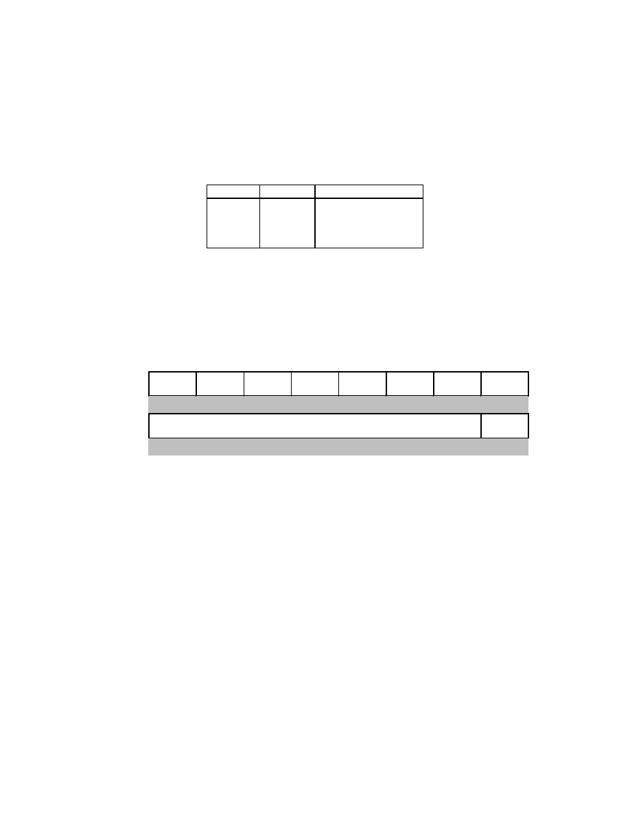
Table 2 - Internal I/O Space Mapping
BANK0
BANK1
BANK2
BANK3
0 TCR
CONFIG MMU
COMMAND MT0-1
2 EPH
STATUS
BASE
PNR
MT2-3
4 RCR
IA0-1
FIFO
PORTS MT4-5
6 COUNTER
IA2-3
POINTER
MT6-7
8 MIR
IA4-5
DATA
MGMT
A MCR
GENERAL
DATA
REVISION
C RESERVED
(0)
CONTROL
INTERRUPT
ERCV
E
BANK SELECT
BANK SELECT
BANK SELECT
BANK SELECT
A special BANK (BANK7) exists to support the addition of external registers.

SMSC DS ≠ LAN91C100FD REV. B
Page 19
Rev. 05/31/2000
BANK SELECT REGISTER
OFFSET NAME
TYPE
SYMBOL
E BANK
SELECT
REGISTER
READ/WRITE BSR
HIGH
BYTE
0 0 1 1 0 0 1 1
0
0
1
1
0
0
1
1
LOW
BYTE
BS2
BS1
BS0
X
X
X
X
X
0
0
0
BS2, BS1, BS0 Determine the bank presently in use. This register is always accessible and is used to select the
register bank in use.
The upper byte always reads as 33h and can be used to help determine the I/O location of the LAN91C100FD.
The BANK SELECT REGISTER is always accessible regardless of the value of BS0-2.
Note that the bank select register can be accessed as a doubleword at offset Ch, as a word at offset Eh, or as at
offset Fh, however a doubleword write to offset Ch will write the BANK SELECT REGISTER but will not write the
registers Ch and Dh.
BANK 7 has no internal registers other than the BANK SELECT REGISTER itself. On valid cycles where BANK7 is
selected (BS0=BS1=BS2=1), and A3=0, nCSOUT is activated to facilitate implementation of external registers.
Note: BANK7 does not exist in LAN91C9x devices. For backward S/W compatibility BANK7 accesses should be done
if the Revision Control register indicates the device is the LAN91C100FD.
BANK 0
OFFSET NAME
TYPE SYMBOL
0 TRANSMIT
CONTROL
REGISTER
READ/WRITE TCR
This register holds bits programmed by the CPU to control some of the protocol transmit options.
HIGH
BYTE
SWFDUP 0
EPH
LOOP
STP
SQET
FDUPLX
MON_
CSN
0 NOCRC
0
0
0
0
0
0
0
0
LOW
BYTE
PAD_EN
0 0 0 0
FORCOL
LOOP
TXENA
0
0
0
0
0
0
0
0
SWFDUP - Enables Switched Full Duplex mode. In this mode, transmit state machine is inhibited from recognizing carrier
sense, so deferrals will not occur. Also inhibits collision count, therefore, the collision related status bits in the EPHSR are
not valid (CTR_ROL, LATCOL, SQET, 16COL, MUL COL, and SNGL COL). Uses COL100 as flow control, limiting
backoff and jam to 1 clock each before inter-frame gap, then retry will occur after IFG. If COL100 is active during
preamble, full preamble will be output before jam. When SWFDUP is high, the values of FDUPLX and MON_CSN have no
effect. This bit should be low for non-MII operation.
EPH_LOOP - Internal loopback at the EPH block. Serial data is internally looped back when set. Defaults low. When
EPH_LOOP is high the following transmit outputs are forced inactive: TXD0-TXD3 = 0h, TXEN100 = TXEN = 0, TXD = 1.
The following and external inputs are blocked: CRS=CRS100=0, COL=COL100=0, RX_DV= RX_ER=0.

SMSC DS ≠ LAN91C100FD REV. B
Page 20
Rev. 05/31/2000
STP_SQET - Stop transmission on SQET error. If set, stops and disables transmitter on SQE test error. Does not stop on
SQET error and transmits next frame if clear. Defaults low.
FDUPLX - When set it enables Full Duplex operation. This will cause frames to be received if they pass the address filter
regardless of the source for the frame. When clear the node will not receive a frame sourced by itself.
MON_CSN - When set the LAN91C100FD monitors carrier while transmitting. It must see its own carrier by the end of the
preamble. If it is not seen, or if carrier is lost during transmission, the transmitter aborts the frame without CRC and turns
itself off and sets the LOST CARR bit in the EPHSR. When this bit is clear the transmitter ignores its own carrier. Defaults
low. Should be 0 for MII operation.
NOCRC - Does not append CRC to transmitted frames when set. Allows software to insert the desired CRC. Defaults to
zero, namely CRC inserted.
PAD_EN - When set, the LAN91C100FD will pad transmit frames shorter than 64 bytes with 00. Does not pad frames
when reset
FORCOL - When set, the FORCOL bit will force a collision by not deferring deliberately. This bit is set and cleared only by
the CPU. When TXENA is enabled with no packets in the queue and while the FORCOL bit is set, the LAN91C100FD will
transmit a preamble pattern the next time a carrier is seen on the line. If a packet is queued, a preamble and SFD will be
transmitted. This bit defaults low to normal operation. NOTE: The LATCOL bit in the EPHSR, setting up as a result of
FORCOL, will reset TXENA to 0. In order to force another collision, TXENA must be set to 1 again.
LOOP - Loopback. General purpose output port used to control the LBK pin. Typically used to put the PHY chip in
loopback mode.
TXENA - Transmit enabled when set. Transmit is disabled if clear. When the bit is cleared the LAN91C100FD will
complete the current transmission before stopping. When stopping due to an error, this bit is automatically cleared.
BANK 0
OFFSET NAME
TYPE SYMBOL
2
EPH STATUS REGISTER
READ ONLY
EPHSR
This register stores the status of the last transmitted frame. This register value, upon individual transmit packet completion,
is stored as the first word in the memory area allocated to the packet. Packet interrupt processing should use the copy in
memory as the register itself will be updated by subsequent packet transmissions. The register can be used for real time
values (like TXENA and LINK OK). If TXENA is cleared the register holds the last packet completion status.
HIGH
BYTE
TX UNRN
LINK_
OK
0
CTR
_ROL
EXC
_DEF
LOST
CARR
LATCOL 0
0
-nLNK pin
0
0
0
0
0
0
LOW
BYTE
TX
DEFR
LTX
BRD
SQET 16COL LTX
MULT
MUL
COL
SNGL
COL
TX_SUC
0
0
0
0
0
0
0
0
TXUNRN - Transmit Under Run. Set if under run occurs, it also clears TXENA bit in TCR. Cleared by setting TXENA high.
This bit may only be set if early TX is being used.
LINK_OK - General purpose input port driven by nLNK pin inverted. Typically used for Link Test. A transition on the value
of this bit generates an interrupt.
CTR_ROL - Counter Roll Over. When set one or more 4 bit counters have reached maximum count (15). Cleared by
reading the ECR register.

SMSC DS ≠ LAN91C100FD REV. B
Page 21
Rev. 05/31/2000
EXC_DEF - Excessive Deferral. When set last/ current transmit was deferred for more than 1518 * 2 byte times. Cleared at
the end of every packet sent.
LOST_CARR - Lost Carrier Sense. When set indicates that Carrier Sense was not present at end of preamble. Valid only if
MON_CSN is enabled. This condition causes TXENA bit in TCR to be reset. Cleared by setting TXENA bit in TCR.
LATCOL - Late collision detected on last transmit frame. If set a late collision was detected (later than 64 byte times into the
frame). When detected the transmitter jams and turns itself off clearing the TXENA bit in TCR. Cleared by setting TXENA in
TCR.
TX_DEFR - Transmit Deferred. When set, carrier was detected during the first 6.4
µs of the inter frame gap. Cleared at the
end of every packet sent.
LTX_BRD - Last transmit frame was a broadcast. Set if frame was broadcast. Cleared at the start of every transmit frame.
SQET - Signal Quality Error Test. In MII, SQET bit is always set after first transmit, except if SWFDUP=1. As a
consequence, the STP_SQET bit in the TCR register cannot be set as it will always result in transmit fatal error. In non-MII
systems, the transmitter opens a 1.6
µs window 0.8 µs after transmission is completed and the receiver returns inactive.
During this window, the transmitter expects to see the SQET signal from the transceiver. The absence of this signal is a
'Signal Quality Error' and is reported in this status bit. Transmission stops and EPH INT is set if STP_SQET is in the TCR is
also set when SQET is set. This bit is cleared by setting TXENA high.
16COL
- 16 collisions reached. Set when 16 collisions are detected for a transmit frame. TXENA bit in TCR is reset.
Cleared when TXENA is set high.
LTX_MULT - Last transmit frame was a multicast. Set if frame was a multicast. Cleared at the start of every transmit
frame.
MULCOL - Multiple collision detected for the last transmit frame. Set when more than one collision was experienced.
Cleared when TX_SUC is high at the end of the packet being sent.
SNGLCOL - Single collision detected for the last transmit frame. Set when a collision is detected. Cleared when TX_SUC is
high at the end of the packet being sent.
TX_SUC - Last transmit was successful. Set if transmit completes without a fatal error. This bit is cleared by the start of a
new frame transmission or when TXENA is set high. Fatal errors are:
16 collisions (1/2 duplex mode only)
SQET fail and STP_SQET = 1 (1/2 duplex mode only)
FIFO Underrun
Carrier lost and MON_CSN = 1 (1/2 duplex mode only)
Late collision (1/2 duplex mode only)

SMSC DS ≠ LAN91C100FD REV. B
Page 22
Rev. 05/31/2000
BANK 0
OFFSET NAME
TYPE SYMBOL
4
RECEIVE CONTROL REGISTER
READ/WRITE
RCR
HIGH
BYTE
SOFT
RST
FILT
CAR
ABORT_
ENB
0 Reserved
Reserved
STRIP
CRC
RXEN
0
0
0
0
0
0
0
0
LOW
BYTE
Reserved Reserved Reserved Reserved Reserved ALMUL PRMS
RX_
ABORT
0
0
0
0
0
0
0
0
SOFT_RST - Software-Activated Reset. Active high. Initiated by writing this bit high and terminated by writing the bit low.
The LAN91C100FD's configuration is not preserved except for Configuration, Base, and IA0-IA5 Registers. EEPROM is
not reloaded after software reset.
FILT_CAR - Filter Carrier. When set filters leading edge of carrier sense for 12 bit times (3 nibble times). Otherwise
recognizes a receive frame as soon as carrier sense is active. (Does NOT filter RX DV on MII!)
ABORT_ENB - Enables abort of receive when collision occurs. Defaults low. When set, the LAN91C100FD will
automatically abort a packet being received when the appropriate collision input is activated (COL100 for MII, COL for non-
MII). This bit has no effect if the SWFDUP bit in the TCR is set.
STRIP_CRC - When set it strips the CRC on received frames. When clear the CRC is stored in memory following the
packet. Defaults low.
RXEN - Enables the receiver when set. If cleared, completes receiving current frame and then goes idle. Defaults low on
reset.
ALMUL - When set accepts all multicast frames (frames in which the first bit of DA is '1'). When clear accepts only the
multicast frames that match the multicast table setting. Defaults low.
PRMS - Promiscuous mode. When set receives all frames. Does not receive its own transmission unless it is in Full
Duplex!
RX_ABORT - This bit is set if a receive frame was aborted due to length longer than 2K bytes. The frame will not be
received. The bit is cleared by RESET or by the CPU writing it low.
Reserved - Must be 0.

SMSC DS ≠ LAN91C100FD REV. B
Page 23
Rev. 05/31/2000
BANK 0
OFFSET NAME
TYPE SYMBOL
6
COUNTER REGISTER
READ ONLY
ECR
Counts four parameters for MAC statistics. When any counter reaches 15 an interrupt is issued. All counters are cleared
when reading the register and do not wrap around beyond 15.
HIGH
BYTE
NUMBER OF EXC. DEFFERED TX
NUMBER OF DEFFERED TX
0
0
0
0
0
0
0
0
LOW
BYTE
MULTIPLE COLLISION COUNT
SINGLE COLLISION COUNT
0
0
0
0
0
0
0
0
Each four bit counter is incremented every time the corresponding event, as defined in the EPH STATUS REGISTER bit
description, occurs. Note that the counters can only increment once per enqueued transmit packet, never faster, limiting the
rate of interrupts that can be generated by the counters. For example if a packet is successfully transmitted after one
collision the SINGLE COLLISION COUNT field is incremented by one. If a packet experiences between 2 to 16 collisions,
the MULTIPLE COLLISION COUNT field is incremented by one. If a packet experiences deferral the NUMBER OF
DEFERRED TX field is incremented by one, even if the packet experienced multiple deferrals during its collision retries.
The COUNTER REGISTER facilitates maintaining statistics in the AUTO RELEASE mode where no transmit interrupts are
generated on successful transmissions.
Reading the register in the transmit service routine will be enough to maintain statistics.
BANK 0
OFFSET NAME
TYPE
SYMBOL
8
MEMORY INFORMATION REGISTER
READ ONLY
MIR
HIGH
BYTE
FREE MEMORY AVAILABLE (IN BYTES * 256 * M)
1
1
1
1
1
1
1
1
LOW
BYTE
MEMORY SIZE (IN BYTES *256 * M)
1
1
1
1
1
1
1
1
FREE MEMORY AVAILABLE - This register can be read at any time to determine the amount of free memory. The register
defaults to the MEMORY SIZE upon reset or upon the RESET MMU command.
MEMORY SIZE - This register can be read to determine the total memory size.
All memory related information is represented in 256 * M byte units, where the multiplier M is determined by the MCR upper
byte.
These register default to FFh, which should be interpreted as 256.
SMSC DS ≠ LAN91C100FD REV. B
Page 24
Rev. 05/31/2000
BANK 0
OFFSET NAME
TYPE
SYMBOL
A MEMORY
CONFIGURATION
REGISTER
Lower Byte -
READ/WRITE
Upper Byte -
READ ONLY
MCR
HIGH
BYTE
MEMORY
SIZE
MULTIPLIER
0
0
1
1
0
1
0
1
LOW
BYTE
MEMORY RESERVED FOR TRANSMIT (IN BYTES * 256 * M)
0
0
0
0
0
0
0
0
MEMORY RESERVED FOR TRANSMIT - Programming this value allows the host CPU to reserve memory to be used
later for transmit, limiting the amount of memory that receive packets can use. When programmed for zero, the memory
allocation between transmit and receive is completely dynamic. When programmed for a non-zero value, the allocation is
dynamic if the free memory exceeds the programmed value, while receive allocation requests are denied if the free
memory is less or equal to the programmed value. This register defaults to zero upon reset. It is not affected by the RESET
MMU command.
The value written to the MCR is a reserved memory space IN ADDITION TO ANY MEMORY CURRENTLY IN USE. If the
memory allocated for transmit plus the reserved space for transmit is required to be constant (rather than grow with
transmit allocations) the CPU should update the value of this register after allocating or releasing memory.
The contents of the MIR as well as the low byte of the MCR are specified in units of 256 * M bytes, where M is the Memory
Size Multiplier. M=2 for the LAN91C100FD. A value of 04h in the lower byte of the MCR is equal to one 2K page (4 * 256
*2 = 2K); since memory must be reserved in multiples of pages, bits 0 and 1 of the MCR should be written to 1 only when
the entire memory is being reserved for transmit (i.e., low byte of MCR = FFh).
BANK1
OFFSET NAME
TYPE
SYMBOL
0 CONFIGURATION
REGISTER
READ/WRITE
CR
The Configuration Register holds bits that define the adapter configuration and are not expected to change during run-time.
This register is part of the EEPROM saved setup.
HIGH
BYTE
MII
SELECT
NO
WAIT
FULL
STEP
0
AUI
SELECT
1
0
1
0
0
0
0
0
LOW
BYTE
1
0
Reserved
INT SEL1
INT SEL0
1
0
1
1
0
0
0
1
MII SELECT - Used to select the network interface port. When set, the LAN91C100FD will use its MII port and interface a
PHY device at the nibble rate. When clear, the LAN91C100FD will use its 10 Mbps ENDEC interface. This bit drives the MII
SEL pin. Switching between ports should be done with transmitter and receiver disabled and no transmit/receive packets in
progress.
NO WAIT - When set, does not request additional wait states. An exception to this are accesses to the Data Register if not
ready for a transfer. When clear, negates IOCHRDY for two to three clocks on any cycle to the LAN91C100FD.
SMSC DS ≠ LAN91C100FD REV. B
Rev. 05/31/2000
FULL STEP - This bit is a general purpose output port. Its inverse value drives pin nFSTEP and it is typically connected to
SEL pin of the LAN83C694. It can be used to select the signaling mode for the AUI or as a general purpose non-volatile
configuration pin. Defaults low.
AUI SELECT - This bit is a general purpose output port. Its value drives pin AUISEL and it is typically connected to MODE1
pin of the LAN83C694. It can be used to select AUI vs. 10BASE-T, or as a general purpose non-volatile configuration pin.
Defaults low.
Reserved - Must be 0.
INT SEL1-0 - Used to select one out of four interrupt pins. The three unused interrupts are tristated.
INT SEL1
INT SEL0
INTERRUPT PIN USED
0
0
1
1
0
1
0
1
INTR0
INTR1
INTR2
INTR3
BANK 1
OFFSET NAME
TYPE
SYMBOL
2
BASE ADDRESS REGISTER
READ/WRITE
BAR
This register holds the I/O address decode option chosen for the LAN91C100FD. It is part of the EEPROM saved setup
and is not usually modified during run-time.
HIGH
BYTE
A15 A14 A13 A9 A8 A7 A6 A5
0
0
0
1
1
0
0
0
LOW
BYTE
Reserved 1
0
0
0
0
0
0
0
1
A15 - A13 and A9 - A5 - These bits are compared against the I/O address on the bus to determine the IOBASE for the
LAN91C100FD`s registers. The 64k I/O space is fully decoded by the LAN91C100FD down to a 16 location space,
therefore the unspecified address lines A4, A10, A11 and A12 must be all zeros.
All bits in this register are loaded from the serial EEPROM. The I/O base decode defaults to 300h (namely, the high byte
defaults to 18h).
Reserved - Must be 0.

SMSC DS ≠ LAN91C100FD REV. B
Page 26
Rev. 05/31/2000
BANK 1
OFFSET NAME
TYPE
SYMBOL
4 THROUGH 9
INDIVIDUAL ADDRESS REGISTERS READ/WRITE
IAR
These registers are loaded starting at word location 20h of the EEPROM upon hardware reset or EEPROM reload. The
registers can be modified by the software driver, but a STORE operation will not modify the EEPROM Individual Address
contents. Bit 0 of Individual Address 0 register corresponds to the first bit of the address on the cable.
LOW
BYTE
ADDRESS 0
0
0
0
0
0
0
0
0
HIGH
BYTE
ADDRESS 1
0
0
0
0
0
0
0
0
LOW
BYTE
ADDRESS 2
0
0
0
0
0
0
0
0
HIGH
BYTE
ADDRESS 3
0
0
0
0
0
0
0
0
LOW
BYTE
ADDRESS 4
0
0
0
0
0
0
0
0
HIGH
BYTE
ADDRESS 5
0
0
0
0
0
0
0
0
BANK 1
OFFSET NAME
TYPE
SYMBOL
A
GENERAL PURPOSE REGISTER
READ/WRITE
GPR
HIGH
BYTE
HIGH DATA BYTE
0
0
0
0
0
0
0
0
LOW
BYTE
LOW DATA BYTE
0
0
0
0
0
0
0
0
This register can be used as a way of storing and retrieving non-volatile information in the EEPROM to be used by the
software driver. The storage is word oriented, and the EEPROM word address to be read or written is specified using the
six lowest bits of the Pointer Register.
This register can also be used to sequentially program the Individual Address area of the EEPROM, that is normally
protected from accidental Store operations.
This register will be used for EEPROM read and write only when the EEPROM SELECT bit in the Control Register is set.
This allows generic EEPROM read and write routines that do not affect the basic setup of the LAN91C100FD.

SMSC DS ≠ LAN91C100FD REV. B
Page 27
Rev. 05/31/2000
BANK 1
OFFSET NAME
TYPE
SYMBOL
C CONTROL
REGISTER
READ/WRITE
CTR
HIGH
BYTE
0
RCV_
BAD
0 1
AUTO
RELEAS
E
0 1 0
0
0
0
1
0
0
1
0
LOW
BYTE
LE
ENABLE
CR
ENABLE
TE
ENABLE
1 0
EEPROM
SELECT
RELOAD STORE
0
0
0
1
0
0
0
0
RCV_BAD - When set, bad CRC packets are received. When clear bad CRC packets do not generate interrupts and their
memory is released. Note: nRXDISC, when asserted, overrides RCV_BAD. Also, RCV_ BAD does not modify the function
of RCV DISCARD in the early receive register.
AUTO RELEASE - When set, transmit pages are released by transmit completion if the transmission was successful (when
TX_SUC is set). In that case there is no status word associated with its packet number, and successful packet numbers are
not even written into the TX COMPLETION FIFO. A sequence of transmit packets will generate an interrupt only when the
sequence is completely transmitted (TX EMPTY INT will be set), or when a packet in the sequence experiences a fatal
error (TX INT will be set). Upon a fatal error TXENA is cleared and the transmission sequence stops. The packet number
that failed, is present in the FIFO PORTS register, and its pages are not released, allowing the CPU to restart the
sequence after corrective action is taken.
LE ENABLE - Link Error Enable. When set it enables the LINK_OK bit transition as one of the interrupts merged into the
EPH INT bit. Clearing the LE ENABLE bit after an EPH INT interrupt, caused by a LINK_OK transition, will acknowledge
the interrupt. LE ENABLE defaults low (disabled).
CR ENABLE - Counter Roll over Enable. When set, it enables the CTR_ROL bit as one of the interrupts merged into the
EPH INT bit. Reading the COUNTER register after an EPH INT interrupt caused by a counter rollover, will acknowledge the
interrupt. CR ENABLE defaults low (disabled).
TE ENABLE - Transmit Error Enable. When set it enables Transmit Error as one of the interrupts merged into the EPH INT
bit. An EPH INT interrupt caused by a transmitter error is acknowledged by setting TXENA bit in the TCR register to 1 or by
clearing the TE ENABLE bit. TE ENABLE defaults low (disabled). Transmit Error is any condition that clears TXENA with
TX_SUC staying low as described in the EPHSR register.
EEPROM SELECT - This bit allows the CPU to specify which registers the EEPROM RELOAD or STORE refers to. When
high, the General Purpose Register is the only register read or written. When low, RELOAD reads Configuration, Base and
Individual Address, and STORE writes the Configuration and Base registers.
RELOAD - When set it will read the EEPROM and update relevant registers with its contents. Clears upon completing the
operation.
STORE - When set, stores the contents of all relevant registers in the serial EEPROM. Clears upon completing the
operation.
Note: When an EEPROM access is in progress the STORE and RELOAD bits will be read back as high. The remaining 14
bits of this register will be invalid. During this time attempted read/write operations, other than polling the EEPROM status,
will NOT have any effect on the internal registers. The CPU can resume accesses to the LAN91C100FD after both bits are
low. A worst case RELOAD operation initiated by RESET or by software takes less than 750
µs.

SMSC DS ≠ LAN91C100FD REV. B
Page 28
Rev. 05/31/2000
BANK2
OFFSET NAME
TYPE
SYMBOL
0
MMU COMMAND REGISTER
WRITE ONLY
BUSY Bit Readable
MMUCR
This register is used by the CPU to control the memory allocation, de-allocation, TX FIFO and RX FIFO control.
The three command bits determine the command issued as described below:
HIGH
BYTE
LOW
BYTE
COMMAND
0 0 N2
N1
N0/BUSY
x
y
z
0
COMMAND SET:
xyz
000
0)
NOOP - NO OPERATION
001
1) ALLOCATE MEMORY FOR TX - N2,N1,N0 defines the amount of memory requested as (value + 1) * 256
bytes. Namely N2,N1,N0 = 1 will request 2 * 256 = 512 bytes. A shift-based divide by 256 of the packet
length yields the appropriate value to be used as N2,N1,N0. Immediately generates a completion code at the
ALLOCATION RESULT REGISTER. Can optionally generate an interrupt on successful completion.
N2,N1,N0 are ignored by the LAN91C100FD but should be implemented in LAN91C100FD software drivers
for LAN9000 compatibility.
010
2) RESET MMU TO INITIAL STATE - Frees all memory allocations, clears relevant interrupts, resets packet
FIFO pointers.
011
3)
REMOVE FRAME FROM TOP OF RX FIFO - To be issued after CPU has completed processing of present
receive frame. This command removes the receive packet number from the RX FIFO and brings the next
receive frame (if any) to the RX area (output of RX FIFO).
100
4) REMOVE AND RELEASE TOP OF RX FIFO - Like 3) but also releases all memory used by the packet
presently at the RX FIFO output. The MMU busy time after issuing REMOVE and RELEASE command
depends on the time when the busy bit is cleared. The time from issuing REMOVE and RELEASE
command on the last receive packet to the time when receive FIFO is empty depends on RX INT bit turning
low. An alternate approach can be checking the read RX FIFO register.
101
5)
RELEASE SPECIFIC PACKET - Frees all pages allocated to the packet specified in the PACKET NUMBER
REGISTER. Should not be used for frames pending transmission. Typically used to remove transmitted
frames, after reading their completion status. Can be used following 3) to release receive packet memory in
a more flexible way than 4).
110
6) ENQUEUE PACKET NUMBER INTO TX FIFO - This is the normal method of transmitting a packet just
loaded into RAM. The packet number to be enqueued is taken from the PACKET NUMBER REGISTER.
111
7) RESET TX FIFOs - This command will reset both TX FIFOs: The TX FIFO holding the packet numbers
awaiting transmission and the TX Completion FIFO.
This command provides a mechanism for
canceling packet transmissions, and reordering or bypassing the transmit queue. The RESET TX FIFOs
command should only be used when the transmitter is disabled. Unlike the RESET MMU command, the
RESET TX FIFOs does not release any memory.
Note 1: Bits N2,N1,N0 bits are ignored by the LAN91C100FD but should be used for command 0 to preserve software
compatibility with the LAN91C92 and future devices. They should be zero for all other commands.

SMSC DS ≠ LAN91C100FD REV. B
Page 29
Rev. 05/31/2000
Note 2: When using the RESET TX FIFOS command, the CPU is responsible for releasing the memory associated with
outstanding packets, or re-enqueuing them. Packet numbers in the completion FIFO can be read via the FIFO
ports register before issuing the command.
Note 3: MMU commands releasing memory (commands 4 and 5) should only be issued if the corresponding packet
number has memory allocated to it.
COMMAND SEQUENCING
A second allocate command (command 1) should not be issued until the present one has completed. Completion is
determined by reading the FAILED bit of the allocation result register or through the allocation interrupt.
A second release command (commands 4, 5) should not be issued if the previous one is still being processed. The BUSY
bit indicates that a release command is in progress. After issuing command 5, the contents of the PNR should not be
changed until BUSY goes low. After issuing command 4, command 3 should not be issued until BUSY goes low.
BUSY BIT - Readable at bit 0 of the MMU command register address. When set indicates that MMU is still processing a
release command. When clear, MMU has already completed last release command. BUSY and FAILED bits are set upon
the trailing edge of command.
BANK 2
OFFSET NAME
TYPE
SYMBOL
2
PACKET NUMBER REGISTER
READ/WRITE
PNR
0
0
PACKET NUMBER AT TX AREA
0
0
0
0
0
0
0
0
PACKET NUMBER AT TX AREA - The value written into this register determines which packet number is accessible
through the TX area. Some MMU commands use the number stored in this register as the packet number parameter. This
register is cleared by a RESET or a RESET MMU Command.
OFFSET NAME
TYPE
SYMBOL
3
ALLOCATION RESULT REGISTER
READ ONLY
ARR
This register is updated upon an ALLOCATE MEMORY MMU command.
FAILED
0
ALLOCATED PACKET NUMBER
1
0
0
0
0
0
0
0
FAILED - A zero indicates a successful allocation completion. If the allocation fails the bit is set and only cleared when the
pending allocation is satisfied. Defaults high upon reset and reset MMU command. For polling purposes, the ALLOC_INT
in the Interrupt Status Register should be used because it is synchronized to the read operation. Sequence:
1) Allocate
Command
2) Poll ALLOC_INT bit until set
3) Read Allocation Result Register
ALLOCATED PACKET NUMBER - Packet number associated with the last memory allocation request. The value is only
valid if the FAILED bit is clear.
Note: For software compatibility with future versions, the value read from the ARR after an allocation request is intended to
be written into the PNR as is, without masking higher bits (provided FAILED = 0).

SMSC DS ≠ LAN91C100FD REV. B
Page 30
Rev. 05/31/2000
BANK 2
OFFSET NAME
TYPE
SYMBOL
4
FIFO PORTS REGISTER
READ ONLY
FIFO
This register provides access to the read ports of the Receive FIFO and the Transmit completion FIFO. The packet
numbers to be processed by the interrupt service routines are read from this register.
HIGH
BYTE
REMPTY
0
RX FIFO PACKET NUMBER
1
0
0
0
0
0
0
0
LOW
BYTE
TEMPTY
0
TX DONE PACKET NUMBER
1
0
0
0
0
0
0
0
REMPTY - No receive packets queued in the RX FIFO. For polling purposes, uses the RCV_INT bit in the Interrupt Status
Register.
TOP OF RX FIFO PACKET NUMBER - Packet number presently at the output of the RX FIFO. Only valid if REMPTY is
clear. The packet is removed from the RX FIFO using MMU Commands 3) or 4).
TEMPTY - No transmit packets in completion queue. For polling purposes, uses the TX_INT bit in the Interrupt Status
Register.
TX DONE PACKET NUMBER - Packet number presently at the output of the TX Completion FIFO. Only valid if TEMPTY
is clear. The packet is removed when a TX INT acknowledge is issued.
Note: For software compatibility with future versions, the value read from each FIFO register is intended to be written into
the PNR as is, without masking higher bits (provided TEMPTY and REMPTY = 0 respectively).
BANK 2
OFFSET NAME
TYPE
SYMBOL
6 POINTER
REGISTER
READ/WRITE
NOT EMPTY is a read
only bit
PTR
HIGH
BYTE
RCV
AUTO
INCR.
READ ETEN NOT
EMPTY
POINTER HIGH
0
0
0
0
0
0
0
0
LOW
BYTE
POINTER LOW
0
0
0
0
0
0
0
0
POINTER REGISTER - The value of this register determines the address to be accessed within the transmit or receive
areas. It will auto-increment on accesses to the data register when AUTO INCR. is set. The increment is by one for every
byte access, by two for every word access, and by four for every double word access. When RCV is set the address refers
to the receive area and uses the output of RX FIFO as the packet number, when RCV is clear the address refers to the
transmit area and uses the packet number at the Packet Number Register.
READ - Determines the type of access to follow. If the READ bit is high the operation intended is a read. If the READ bit is
low the operation is a write. Loading a new pointer value, with the READ bit high, generates a pre-fetch into the Data
Register for read purposes.

SMSC DS ≠ LAN91C100FD REV. B
Page 31
Rev. 05/31/2000
Readback of the pointer will indicate the value of the address last accessed by the CPU (rather than the last pre-fetched).
This allows any interrupt routine that uses the pointer, to save it and restore it without affecting the process being
interrupted. The Pointer Register should not be loaded until the Data Register FIFO is empty. The NOT EMPTY bit of this register
can be read to determine if the FIFO is empty. On reads, if IOCHRDY is not connected to the host, the Data Register should not
be read before 370ns after the pointer was loaded to allow the Data Register FIFO to fill.
If the pointer is loaded using 8 bit writes, the low byte should be loaded first and the high byte last.
ETEN - When set enables EARLY Transmit underrun detection. Normal operation when clear.
NOT EMPTY - When set indicates that the Write Data FIFO is not empty yet. The CPU can verify that the FIFO is empty
before loading a new pointer value. This is a read only bit.
Note: If AUTO INCR. is not set, the pointer must be loaded with a dword aligned value.
BANK 2
OFFSET NAME TYPE
SYMBOL
8 THROUGH Bh
DATA REGISTER
READ/WRITE
DATA
DATA HIGH
X
X
X
X
X
X
X
X
DATA LOW
X
X
X
X
X
X
X
X
DATA REGISTER - Used to read or write the data buffer byte/word presently addressed by the pointer register.
This register is mapped into two uni-directional FIFOs that allow moving words to and from the LAN91C100FD regardless
of whether the pointer address is even, odd or dword aligned. Data goes through the write FIFO into memory, and is pre-
fetched from memory into the read FIFO. If byte accesses are used, the appropriate (next) byte can be accessed through
the Data Low or Data High registers. The order to and from the FIFO is preserved. Byte, word and dword accesses can be
mixed on the fly in any order.
This register is mapped into two consecutive word locations to facilitate double word move operations regardless of the
actual bus width (16 or 32 bits). The DATA register is accessible at any address in the 8 through Ah range, while the
number of bytes being transferred is determined by A1 and nBE0-nBE3. The FIFOs are 12 bytes each.
BANK 2
OFFSET NAME
TYPE
SYMBOL
C
INTERRUPT STATUS REGISTER
READ ONLY
IST
RX_DISC
INT
ERCV INT
EPH INT
RX_OVRN
INT
ALLOC INT
TX EMPTY
INT
TX INT
RCV INT
0
0
0
0
0
1
0
0

SMSC DS ≠ LAN91C100FD REV. B
Page 32
Rev. 05/31/2000
OFFSET NAME
TYPE
SYMBOL
C INTERRUPT
ACKNOWLEDGE
REGISTER
WRITE ONLY
ACK
RX_DISC
INT
ERCV INT
RX_OVRN
INT
TX EMPTY
INT
TX INT
OFFSET NAME
TYPE
SYMBOL
D
INTERRUPT MASK REGISTER
READ/WRITE
MSK
RX_DISC
INT
ERCV INT
EPH INT
RX_OVRN
INT
ALLOC INT
TX EMPTY
INT
TX INT
RCV INT
0
0
0
0
0
0
0
0
This register can be read and written as a word or as two individual bytes.
The Interrupt Mask Register bits enable the appropriate bits when high and disable them when low. An enabled bit being
set will cause a hardware interrupt.
EPH INT - Set when the Ethernet Protocol Handler section indicates one out of various possible special conditions. This bit
merges exception type of interrupt sources, whose service time is not critical to the execution speed of the low level drivers.
The exact nature of the interrupt can be obtained from the EPH Status Register (EPHSR), and enabling of these sources
can be done via the Control Register. The possible sources are:
LINK - Link Test transition
CTR_ROL - Statistics counter roll over
TXENA cleared - A fatal transmit error occurred forcing TXENA to be cleared. TX_SUC will be low and the specific
reason will be reflected by the bits:
TXUNRN - Transmit underrun
SQET - SQE Error
LOST CARR - Lost Carrier
LATCOL - Late Collision
16COL - 16 collisions
RX_DISC INT - Set when the nRXDISC PIN COUNTER in the ERCV register increments to a value of FF. The RX_DISC
INT bit latches the condition for the purpose of being polled or generating an interrupt, and will only be cleared by writing the
acknowledge register with the RX_DISC INT bit set.
RX_OVRN INT - Set when 1) the receiver aborts due to an overrun due to a failed memory allocation, 2) the receiver
aborts due to a packet length of greater than 2K bytes, or 3) the receiver aborts due to the RCV DISCRD bit in the ERCV
register set. The RX_OVRN INT bit latches the condition for the purpose of being polled or generating an interrupt, and will
only be cleared by writing the acknowledge register with the RX_OVRN INT bit set.
ALLOC INT - Set when an MMU request for TX pages allocation is completed. This bit is the complement of the FAILED
bit in the ALLOCATION RESULT register. The ALLOC INT ENABLE bit should only be set following an allocation
command, and cleared upon servicing the interrupt.
TX EMPTY INT - Set if the TX FIFO goes empty, can be used to generate a single interrupt at the end of a sequence of
packets enqueued for transmission. This bit latches the empty condition, and the bit will stay set until it is specifically
cleared by writing the acknowledge register with the TX EMPTY INT bit set. If a real time reading of the FIFO empty is
desired, the bit should be first cleared and then read.

SMSC DS ≠ LAN91C100FD REV. B
Page 33
Rev. 05/31/2000
The TX EMPTY INT ENABLE should only be set after the following steps:
a) a packet is enqueued for transmission
b) the previous empty condition is cleared (acknowledged)
TX INT - Set when at least one packet transmission was completed. The first packet number to be serviced can be read
from the FIFO PORTS register. The TX INT bit is always the logic complement of the TEMPTY bit in the FIFO PORTS
register. After servicing a packet number, its TX INT interrupt is removed by writing the Interrupt Acknowledge Register with
the TX INT bit set.
RCV INT - Set when a receive interrupt is generated. The first packet number to be serviced can be read from the FIFO
PORTS register. The RCV INT bit is always the logic complement of the REMPTY bit in the FIFO PORTS register.
ERCV INT - Early receive interrupt. Set whenever a receive packet is being received, and the number of bytes received
into memory exceeds the value programmed as ERCV THRESHOLD (Bank 3, Offset Ch). ERCV INT stays set until
acknowledged by writing the INTERRUPT ACKNOWLEDGE REGISTER with the ERCV INT bit set.
Note: If the driver uses AUTO RELEASE mode it should enable TX EMPTY INT as well as TX INT. TX EMPTY INT will be
set when the complete sequence of packets is transmitted. TX INT will be set if the sequence stops due to a fatal error on
any of the packets in the sequence.
FIGURE 5 -
INTERRUPT
STRUCTURE
5
4
3
2
1
0
5
4
3
2
1
0
I
N
T
E
R
R
U
P
T
S
T
A
T
U
S
R
E
G
I
S
T
E
R
I
N
T
E
R
R
U
P
T
M
A
S
K
R
E
G
I
S
T
E
R
O
E
n
O
E
n
R
D
I
S
T
1
6
D
A
T
A
B
U
S
D
0
-
7
D
8
-
1
5
E
D
G
E
D
E
T
E
C
T
OR
O
N
L
I
N
K
E
R
R
L
E
M
A
S
K
C
T
R
-
R
O
L
C
R
M
A
S
K
T
E
M
A
S
K
T
X
E
N
A
T
X
_
S
V
C
E
P
H
S
R
I
N
T
E
R
R
U
P
T
S
M
E
R
G
E
D
I
N
T
O
E
P
H
I
N
T
D
2
D
4
D
S
Q
n
Q
T
X
F
I
F
O
E
M
P
T
Y
n
W
R
A
C
K
D
S
Q
n
Q
R
X
_
O
V
R
N
(
E
P
H
S
R
)
A
L
L
O
C
A
T
I
ON
F
A
I
L
E
D
T
X
C
O
M
P
L
E
T
I
O
N
F
I
F
O
N
O
T
E
M
P
T
Y
R
C
V
F
I
F
O
N
O
T
E
M
P
T
Y
R
C
V
I
N
T
T
X
I
N
T
T
X
E
M
P
T
Y
I
N
T
A
L
L
O
C
I
N
T
R
X
_
O
V
R
N
I
N
T
E
P
H
I
N
T
I
N
T
M
A
I
N
I
N
T
E
R
R
U
P
T
S
E
R
C
V
I
N
T
6
6

SMSC DS ≠ LAN91C100FD REV. B
Page 34
Rev. 05/31/2000
BANK3
OFFSET NAME
TYPE
SYMBOL
0 THROUGH 7
MULTICAST TABLE READ/WRITE MT
LOW
BYTE
MULTICAST TABLE 0
0
0
0
0
0
0
0
0
HIGH
BYTE
MULTICAST TABLE 1
0
0
0
0
0
0
0
0
LOW
BYTE
MULTICAST TABLE 2
0
0
0
0
0
0
0
0
HIGH
BYTE
MULTICAST TABLE 3
0
0
0
0
0
0
0
0
LOW
BYTE
MULTICAST TABLE 4
0
0
0
0
0
0
0
0
HIGH
BYTE
MULTICAST TABLE 5
0
0
0
0
0
0
0
0
LOW
BYTE
MULTICAST TABLE 6
0
0
0
0
0
0
0
0
HIGH
BYTE
MULTICAST TABLE 7
0
0
0
0
0
0
0
0
The 64 bit multicast table is used for group address filtering. The hash value is defined as the six most significant bits of the
CRC of the destination addresses. The three msb's determine the register to be used (MT0-MT7), while the other three
determine the bit within the register.
If the appropriate bit in the table is set, the packet is received.
If the ALMUL bit in the RCR register is set, all multicast addresses are received regardless of the multicast table values.
Hashing is only a partial group addressing filtering scheme, but being the hash value available as part of the receive status
word, the receive routine can reduce the search time significantly. With the proper memory structure, the search is limited
to comparing only the multicast addresses that have the actual hash value in question.
SMSC DS ≠ LAN91C100FD REV. B
Page 35
Rev. 05/31/2000
BANK 3
OFFSET NAME
TYPE
SYMBOL
8 MANAGEMENT
INTERFACE
READ/WRITE MGMT
HIGH
BYTE
FLTST
MSK_
CRS100
0
0
1
1
0
0
1
1
LOW
BYTE
MDOE
MCLK
MDI
MDO
0
0
1
1
0
0
MDI Pin
0
FLTST - Facilitates the inclusion of packet forwarding information on the receive packet memory structure. When 0, RD0-
RD7 is always driven. When 1, RD0-RD7 is floated during RECEIVE FRAME STATUS WORD writes (RA2-RA16=0,
RCVDMA=1, nRWE0-nRWE3=0).
MSK_CRS100 - Disables CRS100 detection during transmit in half duplex mode (SWFDUP=0).
MDO - MII Management output. The value of this bit drives the MDO pin.
MDI - MII Management input. The value of the MDI pin is readable using this bit.
MDCLK - MII Management clock. The value of this bit drives the MDCLK pin.
MDOE - MII Management output enable. When high pin MDO is driven, when low pin MDO is tri-stated.
The purpose of this interface, along with the corresponding pins is to implement MII PHY management in software.
BANK 3
OFFSET NAME
TYPE
SYMBOL
A
REVISION REGISTER
READ ONLY
REV
HIGH
BYTE
0
0
1
1
0
0
1
1
LOW
BYTE
CHIP REV
1
0
0
0
0
0
0
0
CHIP - Chip ID. Can be used by software drivers to identify the device used.
REV - Revision ID. Incremented for each revision of a given device.
OFFSET NAME
TYPE
SYMBOL
C
EARLY RCV REGISTER
READ/WRITE
ERCV
HIGH
BYTE
nRXDISC PIN COUNTER
0
0
0
0
0
0
0
0
LOW
BYTE
RCV
DISCRD
0 0
ERCV
THRESHOLD
0
0
0
1
1
1
1
1
SMSC DS ≠ LAN91C100FD REV. B
Page 36
Rev. 05/31/2000
nRXDISC PIN COUNTER - 8-bit counter increments when a packet is discarded due to the nRXDISC pin being active.
This counter will be reset to 00 when read. A count of FF will set the RX_DISC INT. The count will wrap around to 00 after
FF.
RCV DISCRD - Set to discard a packet being received. Will discard packets only in the process of being received. When
set prior to the end of receive packet, bit 4 (RXOVRN) of the interrupt status register will be set to indicate that the packet
was discarded. Otherwise, the packet will be received normally and bit 0 set (RCVINT) in the interrupt status register. RCV
DISCRD is self clearing.
ERCV THRESHOLD - Threshold for ERCV interrupt. Specified in 64 byte multiples. Whenever the number of bytes written
in memory for the presently received packet exceeds the ERCV THRESHOLD, ERCV INT bit of the INTERRUPT STATUS
REGISTER is set.
BANK7
OFFSET NAME
TYPE
SYMBOL
0 THROUGH 7
EXTERNAL REGISTERS
nCSOUT is driven low by the LAN91C100FD when a valid access to the EXTERNAL REGISTER range occurs.
HIGH
BYTE
EXTERNAL R/W REGISTER
LOW
BYTE
EXTERNAL R/W REGISTER
CYCLE
nCSOUT
LAN91C100FD DATA BUS
AEN=0
A3=0
A4-15 matches I/O BASE
BANK SELECT = 7
Driven low. Transparently latched on
nADS rising edge.
Ignored on writes.
Tri-stated on reads.
BANK SELECT = 4,5,6
High
Ignore cycle.
Otherwise
High
Normal LAN91C100FD cycle.

SMSC DS ≠ LAN91C100FD REV. B
Page 37
Rev. 05/31/2000
TYPICAL FLOW OF EVENTS FOR TRANSMIT
S/W DRIVER
MAC SIDE
1 ISSUE ALLOCATE MEMORY FOR TX - N
BYTES - the MMU attempts to allocate N bytes
of RAM.
2 WAIT FOR SUCCESSFUL COMPLETION
CODE - Poll until the ALLOC INT bit is set or
enable its mask bit and wait for the interrupt.
The TX packet number is now at the Allocation
Result Register.
3 LOAD TRANSMIT DATA - Copy the TX packet
number into the Packet Number Register. Write
the Pointer Register, then use a block move
operation from the upper layer transmit queue
into the Data Register.
4 ISSUE "ENQUEUE PACKET NUMBER TO TX
FIFO" - This command writes the number
present in the Packet Number Register into the
TX FIFO. The transmission is now enqueued.
No further CPU intervention is needed until a
transmit interrupt is generated.
5
The enqueued packet will be transferred to the
MAC block as a function of TXENA (nTCR) bit
and of the deferral process (1/2 duplex mode
only) state.
6
Upon transmit completion the first word in
memory is written with the status word. The
packet number is moved from the TX FIFO into
the TX completion FIFO. Interrupt is generated
by the TX completion FIFO being not empty.
7 SERVICE INTERRUPT - Read Interrupt Status
Register. If it is a transmit interrupt, read the TX
Done Packet Number from the Fifo Ports
Register. Write the packet number into the
Packet Number Register. The corresponding
status word is now readable from memory. If
status word shows successful transmission,
issue RELEASE packet number command to
free up the memory used by this packet.
Remove packet number from completion FIFO
by writing TX INT Acknowledge Register.

SMSC DS ≠ LAN91C100FD REV. B
Page 38
Rev. 05/31/2000
TYPICAL FLOW OF EVENTS FOR RECEIVE
S/W DRIVER
MAC SIDE
1 ENABLE RECEPTION - By setting the RXEN
bit.
2
A packet is received with matching address.
Memory is requested from MMU. A packet
number is assigned to it. Additional memory is
requested if more pages are needed.
3
The internal DMA logic generates sequential
addresses and writes the receive words into
memory. The MMU does the sequential to
physical address translation. If overrun, packet
is dropped and memory is released.
4
When the end of packet is detected, the status
word is placed at the beginning of the receive
packet in memory. Byte count is placed at the
second word. If the CRC checks correctly the
packet number is written into the RX FIFO. The
RX FIFO, being not empty, causes RCV INT
(interrupt) to be set. If CRC is incorrect the
packet memory is released and no interrupt will
occur.
5 SERVICE INTERRUPT - Read the Interrupt
Status Register and determine if RCV INT is set.
The next receive packet is at receive area. (Its
packet number can be read from the FIFO Ports
Register). The software driver can process the
packet by accessing the RX area, and can move
it out to system memory if desired. When
processing is complete the CPU issues the
REMOVE AND RELEASE FROM TOP OF RX
command to have the MMU free up the used
memory and packet number.

SMSC DS ≠ LAN91C100FD REV. B
Page 39
Rev. 05/31/2000
FIGURE 6 - INTERRUPT SERVICE ROUTINE
ISR
Save Bank Select & Address
Ptr Registers
Mask SMC91C100FD
Interrupts
Read Interrupt Register
Call TX INTR or TXEMPTY
INTR
TX INTR?
Get Next TX
RX INTR?
Yes
No
No
Yes
Call RXINTR
ALLOC INTR?
No
Yes
Write Allocated Pkt # into
Packet Number Reg.
Write Ad Ptr Reg. & Copy Data
& Source Address
Enqueue Packet
Packet
Available for
Transmission?
Yes
No
Call ALLOCATE
EPH INTR?
No
Yes
Call EPH INTR
Set "Ready for Packet" Flag
Return Buffers to Upper Layer
Disable Allocation Interrupt
Mask
Restore Address Pointer &
Bank Select Registers
Unmask SMC91C100FD
Interrupts
Exit ISR

SMSC DS ≠ LAN91C100FD REV. B
Page 40
Rev. 05/31/2000
RX INTR
Write Ad. Ptr. Reg. & Read
Word 0 from RAM
Destination
Multicast?
Read Words 2, 3, 4 from RAM
for Address Filtering
Address
Filtering Pass?
Status Word
OK?
Do Receive Lookahead
Get Copy Specs from Upper
Layer
Okay to
Copy?
Copy Data Per Upper Layer
Specs
Issue "Remove and Release"
Command
Return to ISR
Yes
No
Yes
No
No
Yes
No
Yes
FIGURE 7 - RX INTR
SMSC DS ≠ LAN91C100FD REV. B
Page 41
Rev. 05/31/2000
Write Into Packet Number
Register
TX Status
OK?
TX INTR
Save Pkt Number Register
Read TXDONE Pkt # from
FIFO Ports Reg.
Immediately Issue "Release"
Command
Acknowledge TXINTR
Read TX INT Again
Return to ISR
No
Yes
Read Status Word from RAM
Update Statistics
Re-Enable TXENA
Update Variables
TX INT = 0?
Restore Packet Number
Yes
No
Write Address Pointer Register
FIGURE 8 - TX INTR
SMSC DS ≠ LAN91C100FD REV. B
Page 42
Rev. 05/31/2000
FIGURE 9 - TXEMPTY INTR (ASSUMES AUTO RELEASE OPTION SELECTED)
TXEMPTY INTR
Write Acknowledge Reg. with
TXEMPTY Bit Set
Read TXEMPTY & TX INTR
Acknowledge TXINTR
Re-Enable TXENA
Return to ISR
Issue "Release" Command
Restore Packet Number
TXEMPTY = 0
&
TXINT = 0
(Waiting for Completion)
TXEMPTY = X
&
TXINT = 1
(Transmission Failed)
TXEMPTY = 1
&
TXINT = 0
(Everything went through
successfully)
Read Pkt. # Register & Save
Write Address Pointer
Register
Read Status Word from RAM
Update Statistics
Update Variables
SMSC DS ≠ LAN91C100FD REV. B
Page 43
Rev. 05/31/2000
FIGURE 10 - DRIVE SEND AND ALLOCATE ROUTINES
ALLOCATE
Issue "Allocate Memory"
Command to MMU
Read Interrupt Status Register
Enqueue Packet
Set "Ready for Packet" Flag
Return
Copy Remaining TX Data
Packet into RAM
Return Buffers to Upper Layer
Write Allocated Packet into
Packet # Register
Write Address Pointer Register
Copy Part of TX Data Packet
into RAM
Write Source Address into
Proper Location
Store Data Buffer Pointer
Clear "Ready for Packet" Flag
Enable Allocation Interrupt
Allocation
Passed?
Yes
No
DRIVER SEND
Choose Bank Select
Register 2
Call ALLOCATE
Exit Driver Send
Read Allocation Result
Register

SMSC DS ≠ LAN91C100FD REV. B
Page 44
Rev. 05/31/2000
MEMORY PARTITIONING
Unlike other controllers, the LAN91C100FD does not require a fixed memory partitioning between transmit and
receive resources. The MMU allocates and de-allocates memory upon different events. An additional mechanism
allows the CPU to prevent the receive process from starving the transmit memory allocation.
Memory is always requested by the side that needs to write into it, that is: the CPU for transmit or the MAC for
receive. The CPU can control the number of bytes it requests for transmit but it cannot determine the number of
bytes the receive process is going to demand. Furthermore, the receive process requests will be dependent on
network traffic, in particular on the arrival of broadcast and multicast packets that might not be for the node, and that
are not subject to upper layer software flow control.
In order to prevent unwanted traffic from using too much memory, the CPU can program a "memory reserved for
transmit" parameter. If the free memory falls below the "memory reserved for transmit" value, MMU requests from the
MAC block will fail and the packets will overrun and be ignored. Whenever enough memory is released, packets can
be received again. If the reserved value is too large, the node might lose data which is an abnormal condition. If the
value is kept at zero, memory allocation is handled on first-come first-served basis for the entire memory capacity.
Note that with the memory management built into the LAN91C100FD, the CPU can dynamically program this
parameter. For instance, when the driver does not need to enqueue transmissions, it can allow more memory to be
allocated for receive (by reducing the value of the reserved memory). Whenever the driver needs to burst
transmissions it can reduce the receive memory allocation. The driver program the parameter as a function of the
following variables:
1) Free memory (read only register)
2) Memory size (read only register)
The reserved memory value can be changed on the fly. If the MEMORY RESERVED FOR TX value is increased
above the FREE MEMORY, receive packets in progress are still received, but no new packets are accepted until the
FREE MEMORY increases above the MEMORY RESERVED value.
INTERRUPT GENERATION
The interrupt strategy for the transmit and receive processes is such that it does not represent the bottleneck in the
transmit and receive queue management between the software driver and the controller. For that purpose there is no
register reading necessary before the next element in the queue (namely transmit or receive packet) can be handled
by the controller. The transmit and receive results are placed in memory.
The receive interrupt will be generated when the receive queue (FIFO of packets) is not empty and receive interrupts
are enabled. This allows the interrupt service routine to process many receive packets without exiting, or one at a
time if the ISR just returns after processing and removing one.
There are two types of transmit interrupt strategies:
1) One interrupt per packet.
2) One interrupt per sequence of packets.
The strategy is determined by how the transmit interrupt bits and the AUTO RELEASE bit are used.
TX INT bit - Set whenever the TX completion FIFO is not empty.
TX EMPTY INT bit - Set whenever the TX FIFO is empty.
AUTO RELEASE - When set, successful transmit packets are not written into completion FIFO, and their memory is
released automatically.
1) One interrupt per packet: enable TX INT, set AUTO RELEASE=0. The software driver can find the completion
result in memory and process the interrupt one packet at a time. Depending on the completion code the driver
will take different actions. Note that the transmit process is working in parallel and other transmissions might be
taking place. The LAN91C100FD is virtually queuing the packet numbers and their status words.
In this case, the transmit interrupt service routine can find the next packet number to be serviced by reading the
TX DONE PACKET NUMBER at the FIFO PORTS register. This eliminates the need for the driver to keep a list
of packet numbers being transmitted. The numbers are queued by the LAN91C100FD and provided back to the
CPU as their transmission completes.

SMSC DS ≠ LAN91C100FD REV. B
Page 45
Rev. 05/31/2000
2) One interrupt per sequence of packets: Enable TX EMPTY INT and TX INT, set AUTO RELEASE=1. TX EMPTY
INT is generated only after transmitting the last packet in the FIFO.
TX INT will be set on a fatal transmit error allowing the CPU to know that the transmit process has stopped and
therefore the FIFO will not be emptied.
This mode has the advantage of a smaller CPU overhead, and faster memory de-allocation. Note that when
AUTO RELEASE=1 the CPU is not provided with the packet numbers that completed successfully.
Note: The pointer register is shared by any process accessing the LAN91C100FD memory. In order to allow
processes to be interruptable, the interrupting process is responsible for reading the pointer value before modifying it,
saving it, and restoring it before returning from the interrupt.
Typically there would be three processes using the pointer:
1) Transmit loading (sometimes interrupt driven)
2) Receive unloading (interrupt driven)
3) Transmit Status reading (interrupt driven).
1) and 3) also share the usage of the Packet Number Register. Therefore saving and restoring the PNR is also
required from interrupt service routines.
FIGURE 11 - INTERRUPT GENERATION FOR TRANSMIT, RECEIVE, MMU
TX
FIFO
TX COMPLETION
FIFO
RX
FIFO
CSMA/CD
LOGICAL
ADDRESS
PACKET #
MMU
PHYSICAL ADDRESS
RAM
CPU ADDRESS
CSMA ADDRESS
RX PACKET
NUMBER
RX FIFO
PACKET NUMBER
PACKET NUMBER
REGISTER
PACK # OUT
M.S. BIT ONLY
'EMPTY'
'NOT EMPTY'
TX DONE
PACKET NUMBER
'NOT EMPTY'
INTERRUPT
STATUS REGISTER
RCV
INT
TX EMPTY
INT
TX
INT
ALLOC
INT
TWO
OPTIONS

SMSC DS ≠ LAN91C100FD REV. B
Page 46
Rev. 05/31/2000
BOARD SETUP INFORMATION
The following parameters are obtained from the EEPROM as board setup information:
ETHERNET INDIVIDUAL ADDRESS
I/O BASE ADDRESS
10BASET or AUI INTERFACE
MII or ENDEC INTERFACE
INTERRUPT LINE SELECTION
All the above mentioned values are read from the EEPROM upon hardware reset. Except for the INDIVIDUAL ADDRESS,
the value of the IOS switches determines the offset within the EEPROM for these parameters, in such a way that many
identical boards can be plugged into the same system by just changing the IOS jumpers.
In order to support a software utility based installation, even if the EEPROM was never programmed, the EEPROM can be
written using the LAN91C100FD. One of the IOS combination is associated with a fixed default value for the key
parameters (I/O BASE, INTERRUPT) that can always be used regardless of the EEPROM based value being
programmed. This value will be used if all IOS pins are left open or pulled high.
The EEPROM is arranged as a 64 x 16 array. The specific target device is the 9346 1024-bit Serial EEPROM. All
EEPROM accesses are done in words. All EEPROM addresses in the spec are specified as word addresses.
REGISTER
EEPROM WORD
ADDRESS
Configuration Register
Base Register
IOS Value * 4
(IOS Value * 4) + 1
INDIVIDUAL ADDRESS 20-22 hex
If IOS2-IOS0 = 7, only the INDIVIDUAL ADDRESS is read from the EEPROM. Currently assigned values are assumed for
the other registers. These values are default if the EEPROM read operation follows hardware reset.
The EEPROM SELECT bit is used to determine the type of EEPROM operation: a) normal or b) general purpose register.
a) NORMAL EEPROM OPERATION - EEPROM SELECT bit = 0
On EEPROM read operations (after reset or after setting RELOAD high) the CONFIGURATION REGISTER and BASE
REGISTER are updated with the EEPROM values at locations defined by the IOS2-0 pins. The INDIVIDUAL ADDRESS
registers are updated with the values stored in the INDIVIDUAL ADDRESS area of the EEPROM.
On EEPROM write operations (after setting the STORE bit) the values of the CONFIGURATION REGISTER and BASE
REGISTER are written in the EEPROM locations defined by the IOS2-IOS0 pins.
The three least significant bits of the CONTROL REGISTER (EEPROM SELECT, RELOAD and STORE) are used to
control the EEPROM. Their values are not stored nor loaded from the EEPROM.
b) GENERAL PURPOSE REGISTER - EEPROM SELECT bit = 1
On EEPROM read operations (after setting RELOAD high) the EEPROM word address defined by the POINTER
REGISTER 6 least significant bits is read into the GENERAL PURPOSE REGISTER.
On EEPROM write operations (after setting the STORE bit) the value of the GENERAL PURPOSE REGISTER is written at
the EEPROM word address defined by the POINTER REGISTER 6 least significant bits.
RELOAD and STORE are set by the user to initiate read and write operations respectively. Polling the value until read low
is used to determine completion. When an EEPROM access is in progress the STORE and RELOAD bits of CTR will

SMSC DS ≠ LAN91C100FD REV. B
Page 47
Rev. 05/31/2000
readback as both bits high. No other bits of the LAN91C100FD can be read or written until the EEPROM operation
completes and both bits are clear. This mechanism is also valid for reset initiated reloads.
Note: If no EEPROM is connected to the LAN91C100FD, for example for some embedded applications, the ENEEP pin
should be grounded and no accesses to the EEPROM will be attempted. Configuration, Base, and Individual Address
assume their default values upon hardware reset and the CPU is responsible for programming them for their final value.
FIGURE 12 - 64 X 16 SERIAL EEPROM MAP
CONFIGURATION REG.
BASE REG.
CONFIGURATION REG.
BASE REG.
CONFIGURATION REG.
BASE REG.
CONFIGURATION REG.
BASE REG.
CONFIGURATION REG.
BASE REG.
CONFIGURATION REG.
BASE REG.
CONFIGURATION REG.
BASE REG.
IA0-1
IA2-3
IA4-5
IOS2-0
WORD ADDRESS
000
0h
1h
4h
5h
8h
9h
Ch
Dh
10h
11h
14h
15h
18h
19h
20h
21h
22h
001
010
011
100
101
110
XXX
16 BITS

SMSC DS ≠ LAN91C100FD REV. B
Page 48
Rev. 05/31/2000
APPLICATION CONSIDERATIONS
The LAN91C100FD is envisioned to fit a few different bus types. This section describes the basic guidelines, system level
implications and sample configurations for the most relevant bus types. All applications are based on buffered
architectures with a private SRAM bus.
FAST ETHERNET SLAVE ADAPTER
Slave non-intelligent board implementing 100 Mbps and 10 Mbps speeds.
Adapter requires:
a) LAN91C100FD
chip
b) Four SRAMs (32k x 8 - 25ns)
c) Serial EEPROM (93C46)
d) Mbps ENDEC and transceiver chip
e) Mbps MII compliant PHY
f)
Some bus specific glue logic
Target systems:
a) VL Local Bus 32 bit systems
b) High-end ISA or non-burst EISA machines
c) EISA 32 bit slave
VL Local Bus 32 Bit SystemsVL Local Bus 32 bit systemsVL Local Bus 32 bit systems
On VL Local Bus and other 32 bit embedded systems the LAN91C100FD is accessed as a 32 bit peripheral in terms of the
bus interface. All registers except the DATA REGISTER will be accessed using byte or word instructions. Accesses to the
DATA REGISTER could use byte, word, or dword instructions.
Table 3 - VL Local Bus Signal Connections
VL BUS
SIGNAL
LAN91C100
SIGNAL
NOTES
A2-A15
A2-A15
Address bus used for I/O space and register decoding, latched by
nADS rising edge, and transparent on nADS low time.
M/nIO
AEN
Qualifies valid I/O decoding - enabled access when low. This signal
is latched by nADS rising edge and transparent on nADS low time.
W/nR
W/nR
Direction of access. Sampled by the LAN91C100FD on first rising
clock that has nCYCLE active. High on writes, low on reads.
nRDYRTN
nRDYRTN
Ready return. Direct connection to VL bus.
nLRDY
nSRDY and some
logic
nSRDY has the appropriate functionality and timing to create the VL
nLRDY except that nLRDY behaves like an open drain output most
of the time.
LCLK
LCLK
Local Bus Clock. Rising edges used for synchronous bus interface
transactions.
nRESET
RESET
Connected via inverter to the LAN91C100FD.
nBE0 nBE1
nBE2 nBE3
nBE0 nBE1
nBE2 nBE3
Byte enables. Latched transparently by nADS rising edge.
nADS
nADS, nCYCLE
Address Strobe is connected directly to the VL bus. nCYCLE is

SMSC DS ≠ LAN91C100FD REV. B
Page 49
Rev. 05/31/2000
Table 3 - VL Local Bus Signal Connections
VL BUS
SIGNAL
LAN91C100
SIGNAL
NOTES
created typically by using nADS delayed by one LCLK.
IRQn
INTR0-INTR3
Typically uses the interrupt lines on the ISA edge connector of VL
bus
D0-D31
D0-D31
32 bit data bus. The bus byte(s) used to access the device are a
function of nBE0-nBE3:
nBE0 nBE1 nBE2 nBE3
0 0 0 0 Double word access
0
0 1 1 Low word access
1 1 0 0 High word access
0 1 1 1 Byte 0 access
1 0 1 1 Byte 1 access
1 1 0 1 Byte 2 access
1 1 1 0 Byte 3 access
Not used = tri-state on reads, ignored on writes. Note that nBE2
and nBE3 override the value of A1, which is tied low in this
application.
nLDEV
nLDEV
nLDEV is a totem pole output. nLDEV is active on valid decodes of
A15-A4 and AEN=0.
UNUSED PINS
VCC nRD
nWR
GND A1
nVLBUS
OPEN nDATACS
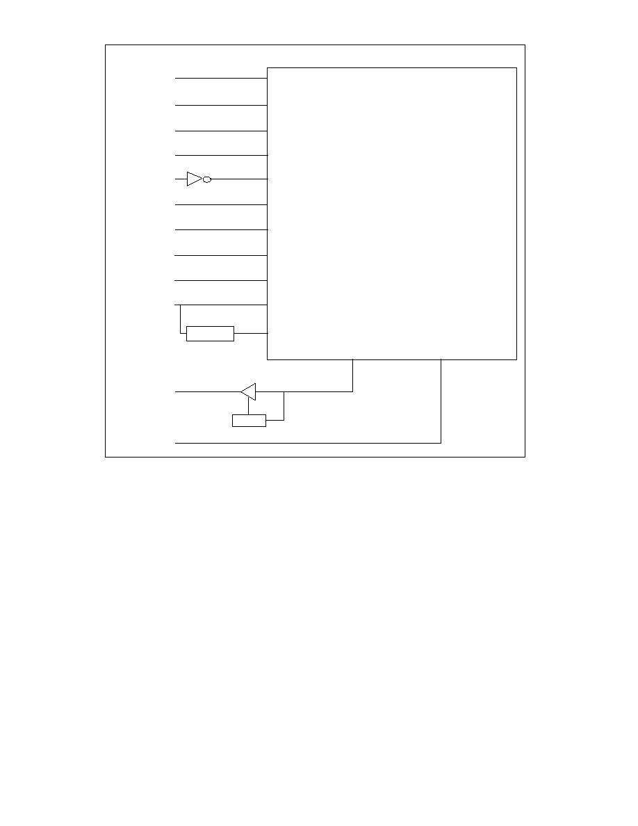
SMSC DS ≠ LAN91C100FD REV. B
Page 50
Rev. 05/31/2000
FIGURE 13 - LAN91C100FD ON VL BUS
W/nR
A2-A15
LCLK
AEN
RESET
INTR0-INTR3
D0-D31
nRDYRTN
nBE0-nBE3
nADS
nCYCLE
nSRDY
nLDEV
LAN91C100FD
W/nR
A2-A15
LCLK
M/nIO
nRESET
IRQn
D0-D31
nRDYRTN
nBE0-nBE3
nADS
nLRDY
nLDEV
delay 1 LCLK
O.C.
simulated
O.C.
VL BUS

SMSC DS ≠ LAN91C100FD REV. B
Page 51
Rev. 05/31/2000
HIGH-END ISA OR NON-BURST EISA MACHINES
On ISA machines, the LAN91C100FD is accessed as a 16 bit peripheral. No support for XT (8 bit peripheral) is provided.
The signal connections are listed in the following table:
Table 4 - High-End ISA or Non-Burst EISA Machines Signal Connectors
ISA BUS
SIGNAL
LAN91C100FD
SIGNAL
NOTES
A1-A15
A1-A15
Address bus used for I/O space and register decoding.
AEN
AEN
Qualifies valid I/O decoding - enabled access when low.
nIORD
nRD
I/O Read strobe - asynchronous read accesses. Address is valid
before leading edge.
nIOWR
nWR
I/O Write strobe - asynchronous write access. Address is valid
before leading edge. Data is latched on trailing edge.
IOCHRDY ARDY
This signal is negated on leading nRD, nWR if necessary. It is then
asserted on CLK rising edge after the access condition is satisfied.
RESET RESET
A0 nBE0
nSBHE nBE1
IRQn INTR0-INTR3
D0-D15
D0-D15
16 bit data bus. The bus byte(s) used to access the device are a
function of nBE0 and nBE1:
nBE0 nBE1 D0-D7
D8-D15
0 0 Lower
Upper
0 1
Lower
Not used
1 0
Not used
Upper
Not used = tri-state on reads, ignored on writes
nIOCS16
nLDEV buffered
nLDEV is a totem pole output. Must be buffered using an open
collector driver. nLDEV is active on valid decodes of A15-A4 and
AEN=0.
UNUSED PINS
GND LCLK
nADS
VCC nBE2
nBE3
nCYCLE W/nR
nRDYRTN
No upper word access.

SMSC DS ≠ LAN91C100FD REV. B
Page 52
Rev. 05/31/2000
FIGURE 14 - LAN91C100FD ON ISA BUS
A1-A15, AEN
RESET
nBE2, nBE3
D0-D15
INTR0-INTR3
nRD
nWR
nBE0
nBE1
nLDEV
LAN91C100FD
A1-A15, AEN
RESET
VCC
D0-D15
nIRQ
nIORD
nIOWR
A0
nSBHE
nIOCS16
O.C.
ISA BUS

SMSC DS ≠ LAN91C100FD REV. B
Page 53
Rev. 05/31/2000
EISA 32 BIT SLAVEEISA 32 bit slave
On EISA the LAN91C100FD is accessed as a 32 bit I/O slave, along with a Slave DMA type "C" data path option. As an
I/O slave, the LAN91C100FD uses asynchronous accesses. In creating nRD and nWR inputs, the timing information is
externally derived from nCMD edges. Given that the access will be at least 1.5 to 2 clocks (more than 180ns at least) there
is no need to negate EXRDY, simplifying the EISA interface implementation. As a DMA Slave, the LAN91C100FD accepts
burst transfers and is able to sustain the peak rate of one doubleword every BCLK. Doubleword alignment is assumed for
DMA transfers. Up to three extra bytes in the beginning and at the end of the transfer should be moved by the CPU using
I/O accesses to the Data Register. The LAN91C100FD will sample EXRDY and postpone DMA cycles if the memory cycle
solicits wait states.
Table 5 - EISA 32 Bit Slave Signal Connections
EISA BUS
SIGNAL
LAN91C100FD
SIGNAL
NOTES
LA2-LA15
A2-A15
Address bus used for I/O space and register decoding, latched
by nADS (nSTART) trailing edge.
M/nIO
AEN
AEN
Qualifies valid I/O decoding - enabled access when low. These
signals are externally ORed. Internally the AEN pin is latched by
nADS rising edge and transparent while nADS is low.
Latched W-R
combined with
nCMD
nRD
I/O Read strobe - asynchronous read accesses. Address is valid
before its leading edge. Must not be active during DMA bursts if
DMA is supported.
Latched W-R
combined with
nCMD
nWR
I/O Write strobe - asynchronous write access. Address is valid
before leading edge . Data latched on trailing edge. Must not be
active during DMA bursts if DMA is supported.
nSTART
nADS
Address strobe is connected to EISA nSTART.
RESDRV RESET
nBE0 nBE1
nBE2 nBE3
nBE0 n BE1
nBE2 nBE3
Byte enables. Latched on nADS rising edge.
IRQn
INTR0-INTR3
Interrupts used as active high edge triggered
D0-D31
D0-D31
32 bit data bus. The bus byte(s) used to access the device are a
function of nBE0-nBE3:
nBE0 nBE1 nBE2 nBE3
0 0 0 0
Double word access
0 0 1 1
Low word access
1 1 0 0 High word access
0 1 1 1 Byte 0 access
1 0 1 1 Byte 1 access
1 1 0
1
Byte 2 access
1 1 1 0 Byte 3 access
Not used = tri-state on reads, ignored on writes. Note that nBE2
and nBE3 override the value of A1, which is tied low in this
application. Other combinations of nBE are not supported by the
LAN91C100FD. Software drivers are not anticipated to generate
them.

SMSC DS ≠ LAN91C100FD REV. B
Page 54
Rev. 05/31/2000
Table 5 - EISA 32 Bit Slave Signal Connections
EISA BUS
SIGNAL
LAN91C100FD
SIGNAL
NOTES
nEX32
nNOWS
(optional
additional logic)
nLDEV
nLDEV is a totem pole output. nLDEV is active on valid decodes
of LAN91C100FD pins A15-A4, and AEN=0. nNOWS is similar
to nLDEV except that it should go inactive on nSTART rising.
nNOWS can be used to request compressed cycles (1.5 BCLK
long, nRD/nWR will be 1/2 BCLK wide).
THE FOLLOWING SIGNALS SUPPORT SLAVE DMA TYPE "C" BURST CYCLES
BCLK
LCLK
EISA Bus Clock. Data transfer clock for DMA bursts.
nDAK<n>
nDATACS
DMA Acknowledge. Active during Slave DMA cycles. Used by
the LAN91C100FD as nDATACS direct access to data path.
nIORC
W/nR
Indicates the direction and timing of the DMA cycles. High
during LAN91C100FD writes, low during LAN91C100FD reads.
nIOWC
nCYCLE
Indicates slave DMA writes.
nEXRDY
nRDYRTN
EISA bus signal indicating whether a slave DMA cycle will take
place on the next BCLK rising edge, or should be postponed.
nRDYRTN is used as an input in the slave DMA mode to bring
in EXRDY.
UNUSED PINS
VCC nVLBUS
GND A1

SMSC DS ≠ LAN91C100FD REV. B
Page 55
Rev. 05/31/2000
FIGURE 15 - LAN91C100FD ON EISA BUS
A2-A15
RESET
AEN
D0-D31
INTR0-INTR3
nBE0-nBE3
nRD
nWR
LCLK
nADS
nLDEV
LAN91C100FD
LA2-LA15
RESDRV
O.C.
EISA BUS
AEN
M/nIO
D0-D31
IRQn
nBE0-nBE3
LATCH +
gates
nCMD
nWR
BCLK
nSTART
nEX32

SMSC DS ≠ LAN91C100FD REV. B
Page 56
Rev. 05/31/2000
OPERATIONAL DESCRIPTION
MAXIMUM GUARANTEED RATINGS*
Operating Temperature Range ................................................................................................................ 0 EC to +70EC
Storage Temperature Range ..............................................................................................................-55EC∞to + 150EC
Lead Temperature Range (soldering, 10 seconds) ............................................................................................ +325EC
Positive Voltage on any pin, with respect to Ground ......................................................................................V
CC
+ 0.3V
Negative Voltage on any pin, with respect to Ground ............................................................................................. -0.3V
Maximum V
CC
........................................................................................................................................................... +7V
*Stresses above those listed above could cause permanent damage to the device. This is a stress rating only and
functional operation of the device at any other condition above those indicated in the operation sections of this
specification is not implied.
Note: When powering this device from laboratory or system power supplies, it is important that the Absolute
Maximum Ratings not be exceeded or device failure can result. Some power supplies exhibit voltage spikes on their
outputs when the AC power is switched on or off. In addition, voltage transients on the AC power line may appear on
the DC output. If this possibility exists, it is suggested that a clamp circuit be used.
DC ELECTRICAL CHARACTERISTICS
(T
A
= 0EC - 70EC, V
CC
= +5.0 V ± 10%)
PARAMETER SYMBOL
MIN
TYP
MAX
UNITS
COMMENTS
I Type Input Buffer
Low Input Level
High Input Level
V
ILI
V
IHI
2.0
0.8
V
V
TTL Levels
IS Type Input Buffer
Low Input Level
High Input Level
Schmitt Trigger Hysteresis
V
ILIS
V
IHIS
V
HYS
2.2
250
0.8
V
V
mV
Schmitt Trigger
Schmitt Trigger
I
CLK
Input Buffer
Low Input Level
High Input Level
V
ILCK
V
IHCK
3.0
0.4
V
V
Input Leakage
(All I and IS buffers except
pins with pullups/pulldowns)
Low Input Leakage
High Input Leakage
I
IL
I
IH
-10
-10
+10
+10
µA
µA
V
IN
= 0
V
IN
= V
CC
IP Type Buffers
Input Current
I
IL
-150
-75
mA
V
IN
= 0
ID Type Buffers
Input Current
I
IH
+75
+150
mA
V
IN
= V
CC

SMSC DS ≠ LAN91C100FD REV. B
Page 57
Rev. 05/31/2000
PARAMETER SYMBOL
MIN
TYP
MAX
UNITS
COMMENTS
O4 Type Buffer
Low Output Level
High Output Level
Output Leakage
V
OL
V
OH
I
OL
2.4
-10
0.4
+10
V
V
µA
I
OL
= 4 mA
I
OH
= -2 mA
V
IN
= 0 to V
CC
I/O4 Type Buffer
Low Output Level
High Output Level
Output Leakage
V
OL
V
OH
I
OL
2.4
-10
0.4
+10
V
V
µA
I
OL
= 4 mA
I
OH
= -2 mA
V
IN
= 0 to V
CC
O12 Type Buffer
Low Output Level
High Output Level
Output Leakage
V
OL
V
OH
I
OL
2.4
-10
0.5
+10
V
V
µA
I
OL
= 12 mA
I
OH
= -6 mA
V
IN
= 0 to V
CC
O16 Type Buffer
Low Output Level
High Output Level
Output Leakage
V
OL
V
OH
I
OL
2.4
-10
0.5
+10
V
V
µA
I
OL
= 16 mA
I
OH
= -8 mA
V
IN
= 0 to V
CC
OD16 Type Buffer
Low Output Level
Output Leakage
V
OL
I
OL
-10
0.5
+10
V
µA
I
OL
= 16 mA
V
IN
= 0 to V
CC
O24 Type Buffer
Low Output Level
High Output Level
Output Leakage
V
OL
V
OH
I
OL
2.4
-10
0.5
+10
V
V
µA
I
OL
= 24 mA
I
OH
= -12 mA
V
IN
= 0 to V
CC
I/O24 Type Buffer
Low Output Level
High Output Level
Output Leakage
V
OL
V
OH
I
OL
2.4
-10
0.5
+10
V
V
µA
I
OL
= 24 mA
I
OH
= -12 mA
V
IN
= 0 to V
CC
Supply Current Active
Supply Current Standby
I
CC
I
CSBY
60
8
95
mA
mA
All Outputs Open

SMSC DS ≠ LAN91C100FD REV. B
Page 58
Rev. 05/31/2000
CAPACITANCE T
A
= 25EC; fc = 1MHz; V
CC
= 5V
LIMITS
PARAMETER SYMBOL
MIN
TYP
MAX
UNIT
TEST
CONDITION
Clock Input Capacitance
C
IN
20
pF
All pins except pin
under test tied to
AC ground
Input Capacitance
C
IN
10
pF
Output Capacitance
C
OUT
20
pF
CAPACITIVE LOAD ON OUTPUTS
nARDY, D0-D31 (non VLBUS)
240 pF
D0-D31
in
VLBUS 45
pF
All
other
outputs
45
pF
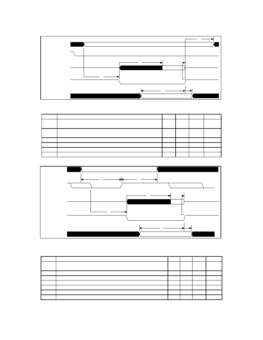
SMSC DS ≠ LAN91C100FD REV. B
Page 59
Rev. 05/31/2000
TIMING DIAGRAMS
FIGURE 16 - ASYNCHRONOUS CYCLE - nADS=0
PARAMETER MIN
TYP
MAX
UNITS
t1
A1-A15, AEN, nBE0-nBE3 Valid and nADS Low Setup to
nRD, nWR Active
25 ns
t2
A1-A15, AEN, nBE0-nBE3 Hold After nRD, nWR Inactive
(Assuming nADS Tied Low)
20 ns
t3
nRD Low to Valid Data
40
ns
t4
nRD High to Data Floating
30
ns
t5
Data Setup to nWR Inactive
30
ns
t5A
Data Hold After nWR Inactive
5
ns
FIGURE 17 - ASYNCHRONOUS CYCLE - USING nADS
PARAMETER MIN
TYP
MAX
UNITS
t1
A1-A15, AEN, nBE0-nBE3 Valid and nADS Low Setup to nRD,
nWR Active
25 ns
t3
nRD Low to Valid Data
40
ns
t4
nRD High to Data Floating
30
ns
t5
Data Setup to nWR Inactive
30
ns
t5A
Data Hold After nWR Inactive
5
ns
t8
A1-A15, AEN, nBE0-nBE3 Setup to nADS Rising
10
ns
t9
A1-A15, AEN, nBE0-nBE3 Hold after nADS Rising
15
ns
t5
t2
t3
t4
t1
t5A
A1-15, AEN, nBE0-nBE3 valid
D0-D31 valid
ADDRESS
nADS
READ DATA
nRD,nWR
WRITE DATA
t8
t9
t5
t3
t4
t1
t5A
A1-A15, AEN, nBE0-nBE3
valid
D0-D31 valid
ADDRESS
nADS
READ DATA
nRD, nWR
WRITE DATA

SMSC DS ≠ LAN91C100FD REV. B
Page 60
Rev. 05/31/2000
FIGURE 18 - ASYNCHRONOUS CYCLE - nADS=0
(nDATACS Used to Select Data Register; Must Be 32 Bit Access)
PARAMETER
MIN
TYP
MAX
UNITS
t1
A1-A15, AEN, nBE0-nBE3 Valid and nADS Low Setup to
nRD, nWR Active
25
ns
t2
A1-A15, AEN, nBE0-nBE3 Hold After nRD, nWR Inactive
(Assuming nADS Tied Low)
20
ns
t3
nRD Low to Valid Data
40
ns
t4
nRD High to Data Floating
30
ns
t5
Data Setup to nWR Inactive
30
ns
t5A
Data Hold After nWR Inactive
5
ns
t5
t2
t3
t4
t1
t5A
D0-D31 valid
nDATACS
nADS
READ DATA
nRD, nWR
WRITE DATA

SMSC DS ≠ LAN91C100FD REV. B
Page 61
Rev. 05/31/2000
FIGURE 19 - BURST WRITE CYCLES - nVLBUS=1
PARAMETER MIN
TYP
MAX
UNITS
t12
nDATACS Setup to Either nCYCLE or W/nR Falling
60
ns
t13
nDATACS Hold after Either nCYCLE or W/nR Rising
30
ns
t14
nRDYRTN Setup to LCLK Falling
15
ns
t15
nRDYRTN Hold after LCLK Falling
2
ns
t17
nCYCLE High and W/nR High Overlap
50
ns
t18
Data Setup to LCLK Rising (Write)
13
ns
t20
Data Hold from LCLK Rising (Write)
5
ns
FIGURE 20 - BURST READ CYCLES - nVLBUS=1
PARAMETER
MIN
TYP
MAX
UNITS
t12 nDATACS Setup to Either nCYCLE or W/nR Falling
60
ns
t13 nDATACS Hold after Either nCYCLE or W/nR Rising
30
ns
t14 nRDYRTN Setup to LCLK Falling
15
ns
t15 nRDYRTN Hold after LCLK Falling
2
ns
t17 nCYCLE High and W/nR High Overlap
50
ns
t19 Data Delay from LCLK Rising (Read)
5*
38**
ns
Note *: (holdt.)
Note **: (Setupt.)
t12
t18
t20
t14
t15
t13
t17
t17
a
b
c
LCLK
nDATACS
W/nR
nCYCLE
WRITE DATA
nRDYRTN
t12
t14
t15
t13
t17
t19
t17
c
a
b
LCLK
nDATACS
W/nR
READ DATA
nRDYRTN
nCYCLE

SMSC DS ≠ LAN91C100FD REV. B
Page 62
Rev. 05/31/2000
FIGURE 21 - ADDRESS LATCHING FOR ALL MODES
PARAMETER MIN
TYP
MAX
UNITS
t8
A1-A15, AEN, nBE0-nBE3 Setup to nADS Rising
10
ns
t9
A1-A15, AEN, nBE0-nBE3 Hold After nADS Rising
15
ns
t25 A4-A15, AEN to nLDEV Delay
20
ns
FIGU
RE 22 - SYNCHRONOUS WRITE CYCLE - nVLBUS=0
PARAMETER MIN
TYP
MAX
UNITS
t8
A1-A15, AEN, nBE0-nBE3 Setup to nADS Rising
10
ns
t9
A1-A15, AEN, nBE0-nBE3 Hold After nADS Rising
15
ns
t10
nCYCLE Setup to LCLK Rising
7
ns
t11
nCYCLE Hold after LCLK Rising (Non-Burst Mode)
3
ns
t16
W/nR Setup to nCYCLE Active
30
ns
t17A W/nR Hold after LCLK Rising with nLRDY Active
5
ns
t18
Data Setup to LCLK Rising (Write)
13
ns
t20
Data Hold from LCLK Rising (Write)
5
ns
t21
nLRDY Delay from LCLK Rising
10
ns
t8
t9
t25
A1-A15, AEN, nBE0-nBE3
nADS
ADDRESS
nLDEV
t18
t20
t10
t11
t17A
t9
t8
t16
t21
t21
D0-D31 valid
A1-A15, AEN, nBE0-nBE3
LCLK
W/nR
ADDRESS
nADS
nCYCLE
WRITE DATA
nSRDY
nDATACS
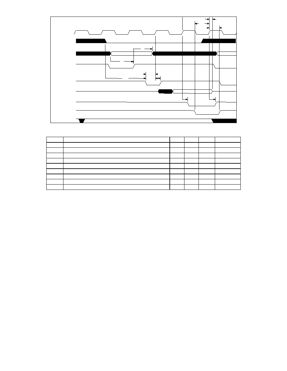
SMSC DS ≠ LAN91C100FD REV. B
Page 63
Rev. 05/31/2000
FIGURE 23 - SYNCHRONOUS READ CYCLE - nVLBUS=0
PARAMETER
MIN TYP MAX UNITS
t8
A1-A15, AEN, nBE0-nBE3 Setup to nADS Rising
10
ns
t9
A1-A15, AEN, nBE0-nBE3 Hold After nADS Rising
15
ns
t10
nCYCLE Setup to LCLK Rising
7
ns
t11
nCYCLE Hold after LCLK Rising (Non-Burst Mode)
3
ns
t16
W/nR Setup to nCYCLE Active
30
ns
t20
Data Hold from LCLK Rising (Read)
5
ns
t21
nLRDY Delay from LCLK Rising
10
ns
t23
nRDYRTN Setup to LCLK Rising
7
ns
t24
nRDYRTN Hold after LCLK Rising
3
ns
t23
t24
t10
t11
t9
t8
t16
t21
t21
D0-D31
A1-A15, AEN, nBE0-nBE3
LCLK
W/nR
ADDRES
nADS
nCYCL
READ
nSRD
RDYRT
nDATAC

SMSC DS ≠ LAN91C100FD REV. B
Page 64
Rev. 05/31/2000
FIGURE 24 - SRAM INTERFACE
PARAMETER
MIN
TYP
MAX
UNITS
t34
Write ≠ RA2-RA16 Setup to nRWE0-nRWE3 Falling
0
ns
t35
Write ≠ RA2-RA16 Hold after nRWE0-nRWE3 Rising
0
ns
t36
Write ≠ RD0-RD31 Setup to nRWE0-nRWE3 Rising
12
ns
t37
Write ≠ RD0-RD31 Hold after nRWE0-nRWE3 Rising
0
ns
t39
Write ≠ nRWE0-nRWE3 Pulse Width
15
ns
t38
Read ≠ RA2-RA16 Valid to RD0-RD31 Valid
25
ns
t51
Read ≠ RD0-RD31 Hold after RA2-RA16 Change
12
ns
t37
t36
t39
t39
t51
t38
t35
t34
READ CYCLE
WRITE CYCLE
RA2-RA16
nRWE0-nRWE3
nROE
RD0-RD31
t38
t51
t38
t51
t38
t51
t38
MULTIPLE READ CYCLES
RA2-RA16
nRWE0-nRWE3
nROE
RD0-RD31
t37
t36
t39
t39
t35
t34
t51
t38
READ CYCLE
WRITE CYCLE
RA2-RA16
nRWE0-nRWE3
nROE
RD0-RD31
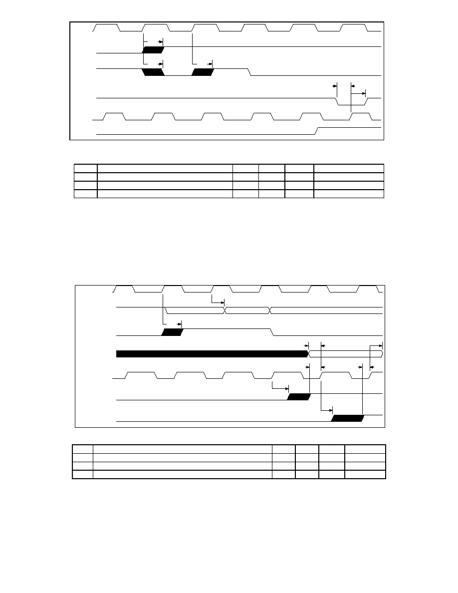
SMSC DS ≠ LAN91C100FD REV. B
Page 65
Rev. 05/31/2000
FIGURE 25 - ENDEC INTERFACE - 10 MBPS
PARAMETER MIN
TYP
MAX
UNITS
t30
TXD, TXEN Delay from TXC Rising
0
40
ns
t31
RXD Setup to RXC Rising
10
ns
t32
RXD Hold After RXC Rising
30
ns
Notes:
1. CRS input might be asynchronous to RXC.
2. RXC starts after CRS goes active. RXC stops after CRS goes inactive.
3. COL is an asynchronous input.
FIGURE 26 - MII INTERFACE
PARAMETER MIN
TYP
MAX
UNITS
t27 TXD0-TXD3, TXEN100 Delay from TX25 Rising
0
15
ns
t28 RXD0-RXD3, RX_DV, RX_ER Setup to RX25 Rising
10
ns
t29 RXD0-RXD3, RX_DV, RX_ER Hold After RX25 Rising
10
ns
t31
t30
t30
t30
t32
TXC
TXEN
TXD
RXD
RXC
CRS
t28
t28
t28
t27
t27
t29
t29
TXD0-TXD3
TXEN100
RXD0-RXD3
RX25
RX_DV
RX_ER

SMSC DS ≠ LAN91C100FD REV. B
Page 66
Rev. 05/31/2000
FIGURE 27 - 208 PIN PQFP PACKAGE OUTLINES
See Detail 'A'
52
D
D1
3
156
105
104
3 157
DETAIL 'A'
R1
R2
4
L
L1
5
E E1
208
1
1
0.10
C
H
A1
A
A2
53
e
2
W
D1/4
E1/4
0
Notes:
Coplanarity is 0.100mm maximum.
Tolerance on the position of the leads is 0.08mm maximum.
Package body dimensions D1 and E1 do not include the mold protrusion. Maximum mold protrusion is 0.25mm.
Dimensions for foot length L when measured at the centerline of the leads are given in the table. Dimension for foot
length L when measured at the gauge plane 0.25mm above the seating plane, is 0.6mm.
Details of pin 1 identifier are optional but must be located within the zone indicated.
6. Controlling dimension: millimeter
1
2
3
4
5
DIM
A
A1
A2
D
D1
E
E1
H
L
L1
e
0
W
R1
R2
MIN
0.05
3.17
30.35
27.90
30.35
27.90
0.09
0.35
NOM
30.60
28.00
30.60
28.00
0.5
1.30
MAX
4.07
0.5
3.67
30.85
28.10
30.85
28.10
0.23
0.65
0∞
0.10
0.20
0.30
0.50 BSC
7∞
0.30

SMSC DS ≠ LAN91C100FD REV. B
Page 67
Rev. 05/31/2000
FIGURE 28 - 208 PIN TQFP PACKAGE OUTLINES
1
2
3
4
5
NOM
30.00
15.00
28.00
30.00
15.00
28.00
0.60
1.00
0.50 BSC
DIM
A
A1
A2
D
D/2
D1
E
E/2
E1
H
L
L1
e
0
W
R1
R2
ccc
ccc
REMARK
Overall Package Height
Standoff
Body Thickness
X Span
1/2 X Span Measure From Centerline
X Body Size
Y Span
1/2 Y Span Measure From Centerline
Y Body Size
Lead Frame Thickness
Lead Foot Length From Centerline
Lead Length
Lead Pitch
Lead Foot Angle
Lead Width
Lead Shoulder Radius
Lead Foot Radius
Coplanarity (Assemblers)
Coplanarity (Test House)
MIN
0.05
1.35
29.80
14.90
27.90
29.80
14.90
27.90
0.09
0.45
0
0.17
0.08
0.08
MAX
1.60
0.15
1.45
30.20
15.10
28.10
30.20
15.10
28.10
0.23
0.75
7
0.27
0.20
0.0762
0.08
Notes:
Controlling Unit: Millimeter.
Tolerance on the position of the leads is 0.04mm maximum.
Package body dimensions D1 and E1 do not include the mold protrusion. Maximum mold protrusion is 0.25mm.
Dimension for foot length L measured at the gauge plane 0.25mm above the seating plane, is 0.78-1.08mm.
Details of pin 1 identifier are optional but must be located within the zone indicated.

SMSC DS ≠ LAN91C100FD REV. B
Page 68
Rev. 05/31/2000
LAN91C100FD REV. B REVISIONS
PAGE(S)
SECTION/FIGURE/ENTRY
CORRECTION
DATE
REVISED
5
Description of Pin Functions
Pin 175 ≠ Changed to active high signal.
05/31/00
20
Table
under
Bank
0
Changed RX_OVRN to 0 on High Byte row.
Removed references to RX_OVRN under table.
05/31/00
64
DC Electrical and Timing
Section
Updated SRAM Interface Timing information. Added
additional timing parameters. Please refer to the
application note titled "LAN91C100FD Minimum
SRAM Access Time Requirement and a List of
Recommended SRAMS" for additional details.
12/17/99