
SMSC DME1737
PRODUCT PREVIEW
Rev. 05-21-04
Data Brief
Product Features
DME1737
Super I/O with Temperature
Sensing, Quiet Auto Fan and
Glue Logic
General Features
-- 3.3 Volt Operation (SIO Block is 5 Volt Tolerant)
-- LPC Interface
-- Programmable Wake-up Event Interface
-- PC99, PC2001 Compliant
-- ACPI 2.0 Compliant
-- Multiplexed Command, Address and Data Bus
-- Serial IRQ Interface Compatible with Serialized IRQ
Support for PCI Systems
-- PME Interface
-- ISA Plug-and-Play Compatible Register Set
-- 25 General Purpose Input/Output Pins
-- System Management Interrupt
AC Power Failure Recovery
Watchdog Timer
2.88MB Super I/O Floppy Disk Controller
-- Licensed CMOS 765B Floppy Disk Controller
-- Software and Register Compatible with SMSC's
Proprietary 82077AA Compatible Core
-- Supports One Floppy Drive
-- Configurable Open Drain/Push-PullOutput Drivers
-- Supports Vertical Recording Format
-- 16-Byte Data FIFO
-- 100% IBM� Compatibility
-- Detects All Overrun and Underrun Conditions
-- Sophisticated Power Control Circuitry (PCC) Including
Multiple Powerdown Modes for Reduced Power
Consumption
-- DMA Enable Logic
-- Data Rate and Drive Control Registers
-- 480 Address, Up to Eight IRQ and Three DMA Options
-- Support 3 Mode FDD
Enhanced Digital Data Separator
-- 2 Mbps, 1 Mbps, 500 Kbps, 300 Kbps, 250 Kbps Data
Rates
-- Programmable Precompensation Modes
Serial Ports
-- Two Full Function Serial Ports
-- High Speed NS16C550A Compatible UARTs with
Send/Receive 16-Byte FIFOs
-- Supports 230k and 460k Baud
-- Programmable Baud Rate Generator
-- Modem Control Circuitry
-- 480 Address and 15 IRQ Options
Infrared Port
-- Multiprotocol Infrared Interface
-- IrDA 1.0 Compliant
-- SHARP ASK IR
-- 480 Addresses, Up to 15 IRQ
Multi-ModeTM Parallel Port with ChiProtectTM
-- Standard Mode IBM PC/XT�, PC/AT�, and PS/2TM
Compatible Bi-directional Parallel Port
-- Enhanced Parallel Port (EPP) Compatible - EPP 1.7
and EPP 1.9 (IEEE 1284 Compliant)
-- IEEE 1284 Compliant Enhanced Capabilities Port
(ECP)
-- ChiProtect Circuitry for Protection
-- 960 Address, Up to 15 IRQ and Three DMA Options
Keyboard Controller
-- 8042 Software Compatible
-- 8 Bit Microcomputer
-- 2k Bytes of Program ROM
-- 256 Bytes of Data RAM
-- Four Open Drain Outputs Dedicated for
Keyboard/Mouse Interface
-- Asynchronous Access to Two Data Registers and One
Status Register
-- Supports Interrupt and Polling Access
-- 8 Bit Counter Timer
-- Port 92 Support
-- Fast Gate A20 and KRESET Outputs
Motherboard GLUE Logic
-- IDE Reset Output
-- (4) Buffered PCI Reset Outputs with software controlled
reset capability - default transparent
-- 3VSB Gate and 3V Gate signal generation
-- Front Panel Reset Debouncing and Power Good Signal
Generation
-- Power Supply Turn On Circuitry with Support for power
button on PS/2 Keyboard
-- Resume Reset Signal Generation
-- SMBus Isolation Circuitry (2 sets external and 1 set
internal for Hardware Monitoring Block)
-- SMBus 2.0 compliant interface for Hardware Monitoring
-- LED Control (2)
Fan Control
-- 5 PWM (Pulse width Modulation) Outputs
-- Low frequency and high frequency PWM support
-- 6 Fan Tachometer Inputs
-- Programmable automatic fan control based on
temperature
-- Interrupt Pin for out-of-limit Fantach Events
-- Fantach events generate PME's and/or Speaker
warning
Temperature Monitor
-- Monitoring of Two Remote Thermal Diodes
-- Internal Ambient Temperature Measurement
-- Limit Comparison of all Monitored Values
-- Interrupt Pin for out-of-limit Temperature Indication
-- Thermal events generate PME's and/or Speaker
warning
-- Configurable offset for internal or external temperature
channels.

ORDERING INFORMATION
Order Number(s):
DME1737-NR for 128 pin QFP package
80 Arkay Drive
Hauppauge, NY 11788
(631)
435-6000
FAX (631) 273-3123
Copyright � SMSC 2004. All rights reserved.
Circuit diagrams and other information relating to SMSC products are included as a means of illustrating typical applications. Consequently, complete
information sufficient for construction purposes is not necessarily given. Although the information has been checked and is believed to be accurate, no
responsibility is assumed for inaccuracies. SMSC reserves the right to make changes to specifications and product descriptions at any time without
notice. Contact your local SMSC sales office to obtain the latest specifications before placing your product order. The provision of this information does
not convey to the purchaser of the described semiconductor devices any licenses under any patent rights or other intellectual property rights of SMSC
or others. All sales are expressly conditional on your agreement to the terms and conditions of the most recently dated version of SMSC's standard
Terms of Sale Agreement dated before the date of your order (the "Terms of Sale Agreement"). The product may contain design defects or errors
known as anomalies which may cause the product's functions to deviate from published specifications. Anomaly sheets are available upon request.
SMSC products are not designed, intended, authorized or warranted for use in any life support or other application where product failure could cause
or contribute to personal injury or severe property damage. Any and all such uses without prior written approval of an Officer of SMSC and further
testing and/or modification will be fully at the risk of the customer. Copies of this document or other SMSC literature, as well as the Terms of Sale
Agreement, may be obtained by visiting SMSC's website at http://www.smsc.com. SMSC is a registered trademark of Standard Microsystems
Corporation ("SMSC"). Product names and company names are the trademarks of their respective holders.
SMSC DISCLAIMS AND EXCLUDES ANY AND ALL WARRANTIES, INCLUDING WITHOUT LIMITATION ANY AND ALL IMPLIED WARRANTIES
OF MERCHANTABILITY, FITNESS FOR A PARTICULAR PURPOSE, TITLE, AND AGAINST INFRINGEMENT AND THE LIKE, AND ANY AND
ALL WARRANTIES ARISING FROM ANY COURSE OF DEALING OR USAGE OF TRADE.
IN NO EVENT SHALL SMSC BE LIABLE FOR ANY DIRECT, INCIDENTAL, INDIRECT, SPECIAL, PUNITIVE, OR CONSEQUENTIAL DAMAGES;
OR FOR LOST DATA, PROFITS, SAVINGS OR REVENUES OF ANY KIND; REGARDLESS OF THE FORM OF ACTION, WHETHER BASED ON
CONTRACT; TORT; NEGLIGENCE OF SMSC OR OTHERS; STRICT LIABILITY; BREACH OF WARRANTY; OR OTHERWISE; WHETHER OR
NOT ANY REMEDY OF BUYER IS HELD TO HAVE FAILED OF ITS ESSENTIAL PURPOSE, AND WHETHER OR NOT SMSC HAS BEEN
ADVISED OF THE POSSIBILITY OF SUCH DAMAGES.
Rev. 05-21-04
2
SMSC DME1737
PRODUCT PREVIEW
Voltage Monitor
-- Monitor Power supplies (5V, +5VTR, +12V, Vccp, Vbat, VTR, and VCC)
-- Limit Comparison of all Monitored Values
-- Interrupt Pin for out-of-limit Voltage Indication
-- Voltage events generate PME's and/or Speaker warning
Security Features
-- Security Key Register (32 byte) for Device Authentication
6 VID (Voltage Identification) Inputs
Phoenix Keyboard BIOS ROM
128 QFP Package

SMSC DME1737
3
Rev. 05-21-04
PRODUCT PREVIEW
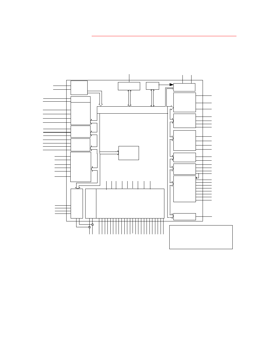
General Description
The DME1737 is a 3.3V (Super I/O Block is 5V tolerant) PC99/PC2001 compliant Super I/O controller
with an LPC interface. DME1737 also includes Hardware Monitoring capabilities, enhanced Security
features, Power Control logic and Motherboard Glue logic.
The DME1737's hardware monitoring capability includes temperature, voltage and fan speed
monitoring. It has the ability to alert the system to out-of-limit conditions and automatically control the
speeds of multiple fans. There are four analog inputs for monitoring external voltages of +5V, +5VTR,
+12V and Vccp (core processor voltage), as well as internal monitoring of the SIO's VCC, VTR, and
Vbat power supplies. The DME1737 includes support for monitoring two external temperatures via
thermal diode inputs and an internal sensor for measuring ambient temperature. The nHWM_INT pin
is implemented to indicate out-of-limit temperature, voltage, and FANTACH conditions. The hardware
monitoring block of the DME1737 is accessible via the System Management Bus (SMBus). The same
interrupt event reported on the nHWM_INT pin also creates PME wakeup events and speaker alarm
annunciation.
The Motherboard Glue logic includes various power management and system logic including
generation of nRSMRST, SMBus buffers, and buffered PCI reset outputs.
The DME1737 incorporates complete legacy Super I/O functionality including an 8042 based keyboard
and mouse controller, an IEEE 1284, EPP, and ECP compatible parallel port, one serial port that is
16C550A UART compatible, one IrDA 1.0 infrared ports, and a floppy disk controller with SMSC's true
CMOS 765B core and enhanced digital data separator, The true CMOS 765B core provides 100%
compatibility with IBM PC/XT and PC/AT architectfures and is software and register compatible with
SMSC's proprietary 82077AA core. System related functionality, which offers flexibility to the system
designer, General Purpose I/O control functions, control of two LED's, and fan control using fan
tachometer inputs and pulse width modulator (PWM) outputs
The DME1737 is ACPI 1.0/2.0 compatible and therefore supports multiple low power-down modes. It
incorporates sophisticated power control circuitry (PCC), which includes support for keyboard and
mouse wake-up events.
The DME1737 supports the ISA Plug-and-Play Standard register set (Version 1.0a). The I/O Address,
DMA Channel and hardware IRQ of each logical device in the DME1737 may be reprogrammed
through the internal configuration registers. There are up to 480 (960 - Parallel Port) I/O address
location options, a Serialized IRQ interface, and Three DMA channels.
Rev. 05-21-04
4
SMSC DME1737
PRODUCT PREVIEW
Block Diagram
Figure 1 DME1737 Block Diagram
LEDs
LE
D
2
*
LE
D
1
*
Internal Bus
(Data, Address, and Control lines)
Power Mgmt
IO_PME_S5*
IO_SMI*
GP1[0:4]*, GP21*,GP22*
GP27*, GP32*,GP33*
GP36*, GP37* ,
GP4[0,2,3]*
GP5[0:1]*, GP6[0:1]*
Note 1: This diagram does not show power and
ground connections.
Note 2: Signal names followed by an asterisk (*) are
located on multifunction pins. This diagram is
designed to show the various functions available on
the chip and should not be used as a pin layout.
CLOCK
GEN
CLK32
CLOCKI
WDT
32 byte
Security
Key
Register
nDSR1, nDTR1
nDCD1, nRI1
Power Control
and Recovery
`
SLP_S3#, SLP_S5#
PW RGD_CPU ,
PW RGD_3V
n3VSB_GAT E
n3V_GATE
nRSMRST
nFPRST, PB_IN#
PW RGD_PS
nH
W
M
_
I
N
T
VI
D
0
VI
D
1
VI
D
2
VI
D
3
VI
D
4
V
I
D5
/
F
A
NTAC
H3
+5
V
_
I
N
+5
V
T
R
_
I
N
VC
C
P
_I
N
+1
2
V
_
I
N
Re
m
o
t
e
1
-
Re
m
o
t
e
1
+
Re
m
o
t
e
2
-
Re
m
o
t
e
2
+
PW
M
1
/
x
T
e
s
t
O
u
t
PW
M
2
P
W
M
3
/
AD
DR
_
E
N
#
F
A
NTAC
H1
F
A
NTAC
H2
F
A
NT
AC
H
4
/
AD
DR
_
S
E
L
PW
M
A
*
,
P
W
M
B
*
F
A
NTAC
HA*
F
A
NTAC
HB*
S
M
b
u
s
SD
A
SC
L
K
Hardware
Monitor
General
Purpose
I/O
IO_PME_S3*
VC
C
VT
R
Vb
a
t
SL
P_
S
3
#
SL
P_
S
5
#
HW
N_
I
N
T
14.
318
M
h
z
96 M
h
z
PC
I
_
R
ESE
T
#
WDT*
SER_IRQ
LAD[3:0]
LFrame#
LDRQ#
PCI_RESET#
PCI_CLK
LPC
Bus Interface
SERIAL
IRQ
SMbus
Isola-
tion
Switch
SDA1
SCLK1
SDA2
SCLK2
SMSC
Proprietary
82077
Compatible
Floppydisk
Controller with
Digital Data
Separator &
W rite Precom-
pensation
nRDATA, nW DATA
nDIR, nSTEP
nMTR0, nTRK0, InNDEX
DRVDEN0*, nW RTPRT
nW GATE, nHDSEL
nDSKCHG, nDS0,
High-Speed
16550A
UART
PORT 1
TXD1*, RXD1
nCTS1, nRTS1*
Multi-Mode
Parallel Port
with
ChiProtect
TM
/FDC
MUX
(see
LPC47B27x)
PD[7,0]
BUSY, SLCT, PE,
nERROR, nACK
nSTROBE, nINIT,
nSLCTIN, nALF
Intruder
Detection
nINTRD_IN
Keyboard/Mouse
8042
controller
KCLK*, KDAT*
MCLK*, MDAT*
A20M*
nKBDRST*
PCI Reset
Outputs
nPCIRST_OUT[1:4]*
nIDE_RSTDRV*
Speaker
SPE
A
K
ER
High-Speed
16550A
UART
PORT 2
TXD2 (IRTX)*,
RXD2 (IRRX)*
DSR2*, DTR2*
DCD2*, RI2*
CTS2*, RTS2 *

SMSC DME1737
5
Rev. 05-21-04
PRODUCT PREVIEW
Package Outline
Figure 2 128 Pin QFP Package Outline, 14X20X2.7 Body, 3.2 mm Footprint
Notes:
1. Controlling Unit: millimeter.
2. Controlling Unit: millimeter.
3. Tolerance on the position of the leads is � 0.04 mm maximum.
4. Package body dimensions D1 and E1 do not include the mold protrusion.
5. Maximum mold protrusion is 0.25 mm.
6. Dimension for foot length L measured at the gauge plane 0.25 mm above the seating plane.
7. Details of pin 1 identifier are optional but must be located within the zone indicated.
Table 1 128 Pin QFP Package Parameters
MIN
NOMINAL
MAX
REMARKS
A
~
~
3.4
Overall Package Height
A1
0.05
~
0.5
Standoff
A2
2.55
~
3.05
Body Thickness
D
23.00
23.20
23.40
X Span
D1
19.90
20.00
20.10
X body Size
E
17.00
17.20
17.40
Y Span
E1
13.90
14.00
14.10
Y body Size
H
0.09
~
0.20
Lead Frame Thickness
L
0.73
0.88
1.03
Lead Foot Length
L1
~
1.60
~
Lead Length
e
0.50 Basic
Lead Pitch
q
0
o
~
7
o
Lead Foot Angle
W
0.10
~
0.30
Lead Width
R1
0.08
~
~
Lead Shoulder Radius
R2
0.08
~
0.30
Lead Foot Radius
ccc
~
~
0.08
Coplanarity