 | –≠–ª–µ–∫—Ç—Ä–æ–Ω–Ω—ã–π –∫–æ–º–ø–æ–Ω–µ–Ω—Ç: EMC1053 | –°–∫–∞—á–∞—Ç—å:  PDF PDF  ZIP ZIP |
SMSC EMC1053
DATASHEET
Revision 0.58 (09-26-05)
Datasheet
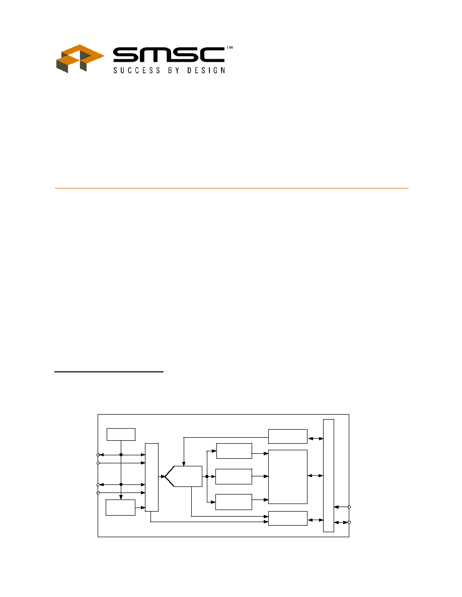
PRODUCT FEATURES
EMC1053
1∞C Triple Temperature
Sensor with Resistance
Error Correction and
Hotter of Two Zones
GENERAL DESCRIPTION
The EMC1053 is a System Management Bus (SMBus)
temperature sensor that monitors up to three
temperature zones, two remote and one local, for PC
and embedded environments. The EMC1053 extended
features include resistance error correction and ideality
factor configuration to eliminate major sources of
temperature measurement error.
1
Monitoring both
diodes of a dual-core CPU is simplified with the Hotter
of Two Zones feature.
The external and internal measurement ranges support
two data ranges (and formats), -64∞C to +127∞C and
-64∞C to +191∞C.
Selectable conversion rates and standby mode support
low-power operation.
APPLICATIONS
Desktop and Notebook Computers
Hardware Management
FEATURES
Resistance Error Correction
Ideality Factor Configuration
Reports Hotter of Two Zones with dual-core CPU
Accepts 2200pF cap for noise suppression
2 Remote Thermal Zones
--
±1∞C Accuracy (40∞C to 80∞C)
-- 0.125
∞C resolution
Internal Thermal Zone
--
±3∞C Accuracy (0∞C to 85∞C)
-- 0.125
∞C resolution
Low Power; 3.0V to 3.6V Supply
Programmable Conversion Rate
SMBus 2.0 Compliant
SIMPLIFIED BLOCK DIAGRAM
1.Patents pending.
EMC1053
Local Temp
Diode
Switching
Current
SMCLK
Local Temp
Register
Configuration
Register
Status Register
S
M
B
u
s
Inte
r
f
ace
Remote Temp
Register 1
Remote Temp
Register 2
SMDATA
11-bit
delta-sigma
ADC
A
n
al
og M
u
x
an
d Ant
i
-A
li
as
Fi
lt
er
DP1
DN1
DP2
DN2
Digital Mux
and
Byte Interlock

ORDER NUMBERS
EMC1053-ACZL-TR FOR 8 PIN, MSOP PACKAGE (ADDRESS - 1001100B) (GREEN, LEAD-FREE)
REEL SIZE IS 4,000 PIECES.
EVALUATION BOARD AVAILABLE UPON REQUEST. (EVB-EMC1053)
80 Arkay Drive
Hauppauge, NY 11788
(631)
435-6000
FAX (631) 273-3123
Copyright © 2005 SMSC or its subsidiaries. All rights reserved.
Circuit diagrams and other information relating to SMSC products are included as a means of illustrating typical applications. Consequently,
complete information sufficient for construction purposes is not necessarily given. Although the information has been checked and is believed to be
accurate, no responsibility is assumed for inaccuracies. SMSC reserves the right to make changes to specifications and product descriptions at any
time without notice. Contact your local SMSC sales office to obtain the latest specifications before placing your product order. The provision of this
information does not convey to the purchaser of the described semiconductor devices any licenses under any patent rights or other intellectual
property rights of SMSC or others. All sales are expressly conditional on your agreement to the terms and conditions of the most recently dated
version of SMSC's standard Terms of Sale Agreement dated before the date of your order (the "Terms of Sale Agreement"). The product may
contain design defects or errors known as anomalies which may cause the product's functions to deviate from published specifications. Anomaly
sheets are available upon request. SMSC products are not designed, intended, authorized or warranted for use in any life support or other
application where product failure could cause or contribute to personal injury or severe property damage. Any and all such uses without prior written
approval of an Officer of SMSC and further testing and/or modification will be fully at the risk of the customer. Copies of this document or other
SMSC literature, as well as the Terms of Sale Agreement, may be obtained by visiting SMSC's website at http://www.smsc.com. SMSC is a
registered trademark of Standard Microsystems Corporation ("SMSC"). Product names and company names are the trademarks of their respective
holders.
SMSC DISCLAIMS AND EXCLUDES ANY AND ALL WARRANTIES, INCLUDING WITHOUT LIMITATION ANY AND ALL IMPLIED
WARRANTIES OF MERCHANTABILITY, FITNESS FOR A PARTICULAR PURPOSE, TITLE, AND AGAINST INFRINGEMENT AND THE LIKE,
AND ANY AND ALL WARRANTIES ARISING FROM ANY COURSE OF DEALING OR USAGE OF TRADE. IN NO EVENT SHALL SMSC BE
LIABLE FOR ANY DIRECT, INCIDENTAL, INDIRECT, SPECIAL, PUNITIVE, OR CONSEQUENTIAL DAMAGES; OR FOR LOST DATA,
PROFITS, SAVINGS OR REVENUES OF ANY KIND; REGARDLESS OF THE FORM OF ACTION, WHETHER BASED ON CONTRACT; TORT;
NEGLIGENCE OF SMSC OR OTHERS; STRICT LIABILITY; BREACH OF WARRANTY; OR OTHERWISE; WHETHER OR NOT ANY REMEDY
OF BUYER IS HELD TO HAVE FAILED OF ITS ESSENTIAL PURPOSE, AND WHETHER OR NOT SMSC HAS BEEN ADVISED OF THE
POSSIBILITY OF SUCH DAMAGES.
1∞C Triple Temperature Sensor with Resistance Error Correction and Hotter of Two Zones
Datasheet
Revision 0.58 (09-26-05)
2
SMSC EMC1053
DATASHEET
1∞C Triple Temperature Sensor with Resistance Error Correction and Hotter of Two Zones
Datasheet
SMSC EMC1053
3
Revision 0.58 (09-26-05)
DATASHEET
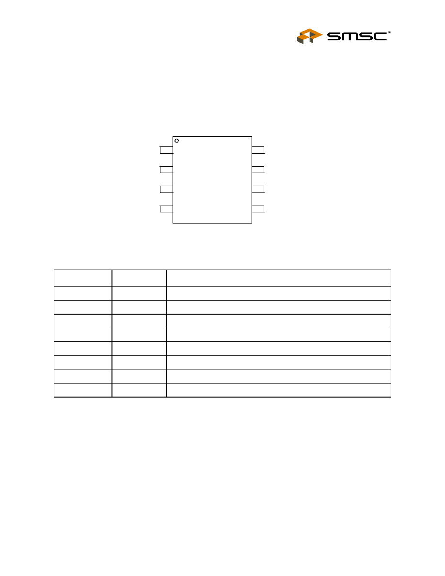
Chapter 1 Pin Function
Figure 1.1 Pin Diagram
Table 1.1 Pin Description
PIN
PIN NO.
DESCRIPTION
DP1
1
Positive Analog Input for Remote Temperature Diode 1
DN1
2
Negative Analog Input for Remote Temperature Diode 1
DP2
3
Positive Analog Input for Remote Temperature Diode 2
DN2
4
Negative Analog Input for Remote Temperature Diode 2
GND
5
Ground
VDD
6
Supply Voltage
SMDATA
7
System Management Bus Data Input/Output, open drain output
SMCLK
8
System Management Bus Clock Input
EMC1053
TOP VIEW
8
7
6
5
1
2
3
4
DP1
DN1
DP2
DN2
SMCLK
SMDATA
VDD
GND

1∞C Triple Temperature Sensor with Resistance Error Correction and Hotter of Two Zones
Datasheet
Revision 0.58 (09-26-05)
4
SMSC EMC1053
DATASHEET
Chapter 2 Electrical Specifications
2.1
Absolute Maximum Ratings
Note: Stresses above those listed could cause damage to the device. This is a stress rating only
and functional operation of the device at any other condition above those indicated in the
operation sections of this specification is not implied. When powering this device from
laboratory or system power supplies, it is important that the Absolute Maximum Ratings not be
exceeded or device failure can result. Some power supplies exhibit voltage spikes on their
outputs when the AC power is switched on or off. In addition, voltage transients on the AC
power line may appear on the DC output. If this possibility exists, it is suggested that a clamp
circuit be used.
2.2
Electrical Specifications
Table 2.1 Absolute Maximum Ratings
DESCRIPTION
RATING
UNIT
Supply Voltage V
DD
-0.3 to 5.0
V
Voltage on SMDATA and SMCLK
pins
-0.3 to 5.5
V
Voltage on any other pin
-0.3 to VDD+0.3
V
Operating Temperature Range
0 to 85
∞C
Storage Temperature Range
-55 to 150
∞C
Lead Temperature Range
Refer to JEDEC
Spec. J-STD-020
Package Thermal Characteristics for MSOP-8
Power Dissipation
TBD
Thermal Resistance (at 0 air flow)
135.9
∞C/W
ESD Rating, All Pins Human Body Model
2000
V
Table 2.2 Electrical Characteristics
V
DD
=3.0V to 3.6V, T
A
= 0
∞C to +85∞C, Typical values at T
A
= 27
∞C unless otherwise noted
PARAMETER
SYMBOL
MIN
TYP
MAX
UNITS
CONDITIONS
DC Power
Supply Voltage
V
DD
3.0
3.3
3.6
V
Average Operating Current
I
DD
340
375
µA
4 conversions/s
See
Table 4.6
.
I
STBY
2
4
µA
Standby mode
Internal Temperature Monitor
Temperature Accuracy
± 1
± 3
∞C
0
∞CT
A
85∞C
Temperature Resolution
0.125
∞C

1∞C Triple Temperature Sensor with Resistance Error Correction and Hotter of Two Zones
Datasheet
SMSC EMC1053
5
Revision 0.58 (09-26-05)
DATASHEET
Note 2.1
300nS rise time max is required for 400kHz bus operation. For lower clock frequencies,
the maximum rise time is (0.1/F
SMB
)+50nS
External Temperature Monitor
Temperature Accuracy
Remote Diode 40
∞C to 80∞C
Remote Diode 0
∞C to 125∞C
± 1
± 3
∞C
∞C
15
∞CT
A
70∞C
0
∞CT
A
85∞C
Temperature Resolution
0.125
∞C
Capacitive Load
C
LOAD
2.5
nF
Connected across
remote diode.
Voltage Tolerance
Voltage at pin (
SMDATA,SMCLK)
V
TOL
-0.3
5.5
V
SMBus Interface (SMDATA,SMCLK)
Input High Level
V
IH
2.0
V
Input Low Level
V
IL
0.8
V
Input High/Low Current
I
IH
/I
IL
-1
1
µ
A
Hysteresis
500
mV
Input Capacitance
5
pF
Output Low Sink Current
6
mA
SMDATA = 0.6V
SMBus Timing
Clock Frequency
F
SMB
10
400
kHz
Spike Suppression
50
ns
Bus free time Start to Stop
T
BUF
1.3
µ
s
Hold time Start
T
HD:STA
0.6
µ
s
Setup time Start
T
SU:STA
0.6
µ
s
Setup time Stop
T
SU:STO
0.6
µ
s
Data Hold Time
T
HD:DAT
0.3
µ
s
Data Setup Time
T
SU:DAT
100
ns
Clock Low Period
T
LOW
1.3
µ
s
Clock High Period
T
HIGH
0.6
µ
s
Clock/Data Fall Time
T
F
*
300
ns
*Min = 20+0.1C
b
ns
Clock/Data Rise Time
T
R
*
300
Note
2.1
ns
*Min = 20+0.1C
b
ns
Capacitive Load (each bus line)
C
b
0.6
400
pF
Table 2.2 Electrical Characteristics (continued)
V
DD
=3.0V to 3.6V, T
A
= 0
∞C to +85∞C, Typical values at T
A
= 27
∞C unless otherwise noted
PARAMETER
SYMBOL
MIN
TYP
MAX
UNITS
CONDITIONS

1∞C Triple Temperature Sensor with Resistance Error Correction and Hotter of Two Zones
Datasheet
Revision 0.58 (09-26-05)
6
SMSC EMC1053
DATASHEET
2.3
System Management Bus Interface Protocol
A host controller, such as an SMSC I/O controller, communicates with the EMC1053 via the two wire
serial interface named SMBus. The SMBus interface is used to read and write registers in the
EMC1053, which is a slave-only device. A detailed timing diagram is shown in
Figure 2.1
.
Figure 2.1 System Management Bus Timing Diagram
The EMC1053 implements a subset of the SMBus specification and supports Write Byte, Read Byte,
Send Byte, and Receive Byte protocols as shown. In the tables that describe the protocol, the "gray"
columns indicate that the slave is driving the bus.
All of the below protocols use the following convention:
2.3.1
Write Byte
The Write Byte is used to write one byte of data to the registers as shown in
Table 2.3
.
2.3.2
Read Byte
The Read Byte protocol is used to read one byte of data from the registers as shown in
Table 2.4
.
2.3.3
Send Byte
The Send Byte protocol is used to set the Internal Address Register to the correct Address as shown
in
Table 2.5
. The Send Byte can be followed by the Receive Byte protocol described in
Table 2.6
to
DATA SENT
TO DEVICE
DATA SENT TO
THE HOST
# of bits sent
# of bits sent
Table 2.3 Write Byte Protocol
START
SLAVE ADDRESS
WR
ACK
COMMAND
ACK
DATA
ACK
STOP
1
7
1
1
8
1
8
1
1
Table 2.4 Read Byte Protocol
START
SLAVE ADDRESS
WR
ACK
COMMAND
ACK
START
SLAVE ADDRESS
RD
ACK
DATA
NACK
STOP
1
7
1
1
8
1
1
7
1
1
8
1
1
SMDATA
SMCLK
T
LOW
T
R
T
HIGH
T
F
T
BUF
T
HD:STA
P
S
S - Start Condition
P - Stop Condition
T
HD:DAT
T
SU:DAT
T
SU:STA
T
HD:STA
P
T
SU:STO
S

1∞C Triple Temperature Sensor with Resistance Error Correction and Hotter of Two Zones
Datasheet
SMSC EMC1053
7
Revision 0.58 (09-26-05)
DATASHEET
read data from the register. The send byte protocol cannot be used to write data - if data is to be
written to a register then the write byte protocol must be used as described in
Section 2.3.1
.
2.3.4
Receive Byte
The Receive Byte protocol is used to read data from a register when the internal register address
pointer is known to be at the right location (e.g. set via Send Byte). This can be used for consecutive
reads of the same register as shown in
Table 2.6
.
2.3.5
SMBus Timing Diagram
The Timing for the SMBus is shown in
Figure 2.1
.
2.4
SMBus Addresses
The EMC1053 may be ordered with one of the 7-bit slave addresses as shown in
Order Numbers
.
Attempting to communicate with the EMC1053 SMBus interface with an invalid slave address or invalid
protocol results in no response from the device and does not affect its register contents. The EMC1053
supports stretching of the SMCLK signal by other devices on the SMBus but will not perform this
operation itself.
2.5
SMBus Timeout
The EMC1053 includes an SMBus timeout feature. Following a 25 ms period of inactivity on the
SMBus, the device will timeout and reset the SMBus interface.
Table 2.5 Send Byte Protocol
START
SLAVE ADDR
WR
ACK
REG. ADDR
ACK
STOP
1
7
1
1
8
1
1
Table 2.6 Receive Byte Protocol
START
SLAVE ADDR
RD
ACK
REG. DATA
NACK
STOP
1
7
1
1
8
1
1
1∞C Triple Temperature Sensor with Resistance Error Correction and Hotter of Two Zones
Datasheet
Revision 0.58 (09-26-05)
8
SMSC EMC1053
DATASHEET
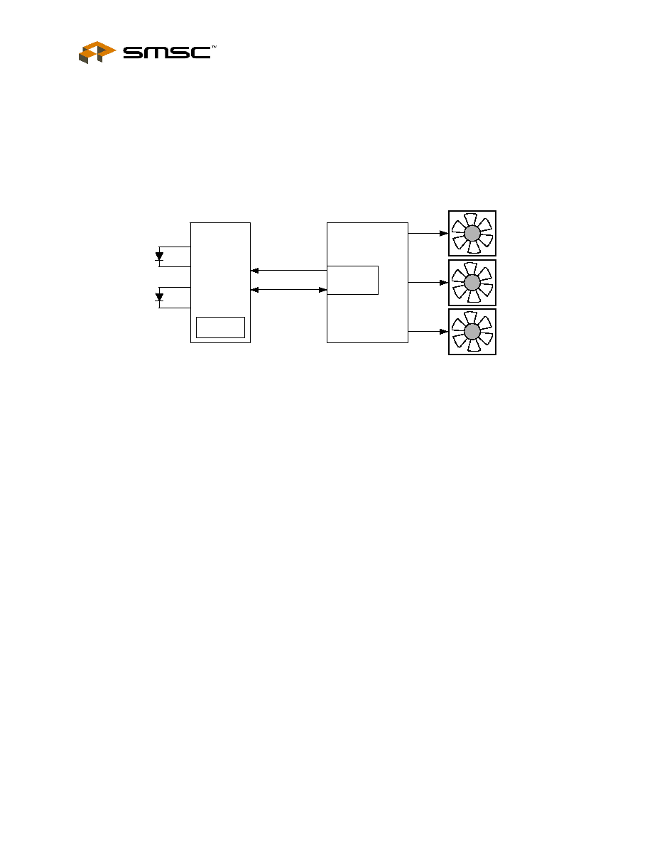
Chapter 3 Product Description
The EMC1053 is an SMBus sensor that is capable of monitoring three temperature zones for use in
a personal computer or embedded environment. The part may be used as a companion to one of
SMSC's broad line of SIO host circuits, or other devices capable of performing the SMBus host
function. A typical system overview is shown in
Figure 3.1
.
3.1
Power Modes
The EMC1053 has two power modes as defined here:
Run Mode - In this mode, the temperature monitors are active and converting at various conversion
rates. The average power dissipation will depend on the conversion rate. When the EMC1053 is
not actively converting a channel, it goes into a lower power wait state where only the oscillator is
running.
Standby Mode- in this mode, the EMC1053 is put into a low power state drawing a maximum
current of 3uA. The SMBus is still operating in standby and a one-shot command may be given
which forces the part to Run Mode temporarily for 1 full set of temperature conversions. The
EMC1053 returns to standby after the one shot conversion is completed.
3.2
One Shot During Standby Mode
The EMC1053 supports a One-Shot command when it is in Standby Mode. Writing to the One-Shot
register will cause the device to power up and perform 1 full set of temperature conversions according
to the selected conversion rate, and then return to the Standby Mode.
3.3
Operation During Run Mode
When the device is active, there are two modes of operation available.
Normal Mode - In this mode, the EMC1053 continuously samples and updates all of its temperature
channels. In this mode of operation, each data channel is measured and loaded into the
appropriate data registers normally.
Hotter of Two Mode - In this mode, the EMC1053 continuously samples and then compares the
two remote zones. The hotter of the two remote zones is loaded into the External Diode 2 data
registers. In addition, the HOTTER bit in the Status register is set or cleared to indicate which
external diode zone was hotter. If the two external zones are exactly equal to each other, then the
Figure 3.1 EMC1053 System Overview
EMC1053
Host
SMBus
Interface
SMBus
Internal
Diode
DP1
DN1
DP2
DN2

1∞C Triple Temperature Sensor with Resistance Error Correction and Hotter of Two Zones
Datasheet
SMSC EMC1053
9
Revision 0.58 (09-26-05)
DATASHEET
HOTTER bit is cleared (set to `0'), and the results of the two remote zones are stored in their
respective registers.
3.3.1
Conversion Rates
The EMC1053 may be configured for different conversion rates based on the system requirements.
The available rates are 1 full set of conversions per second to 16 full sets of conversions per second.
The available conversion rates are shown in
Table 4.6
.
3.3.2
Dynamic Averaging
The EMC1053 temperature channels support a new feature that measures the external diode channels
for an extended period of time based on the selected conversion rate. When Dynamic Averaging is
enabled, the device will automatically adjust the sampling and measurement time for both external
diode channels. This allows the device to average 2x or 4x longer than the normal 11 bit operation
while still maintaining the selected conversion rate. The benefits of Dynamic Averaging are improved
noise rejection due to the longer sampling and measurement time as well as reduced jitter on the
measurement value for the external temperatures.
The Dynamic Averaging applies when a One-Shot command is issued. The device will perform the
desired number of averages during the one-shot operation according to the selected conversion rate.
3.4
Temperature Monitors
In general, thermal diode temperature measurements are based on the change in forward bias voltage
of a diode when operated at two different currents. This
V
BE
is then proportional to absolute
temperature as shown in the following equation:
where:
k = Boltzmann's constant
T = absolute temperature in Kelvin
q = electron charge
= diode ideality factor
Figure 3.2 Block Diagram of Temperature Monitoring Circuit
=
-
=
1
2
_
_
ln
F
F
LOW
BE
HIGH
BE
BE
I
I
q
kT
V
V
V
CPU
substrate
PNP
I
F1
I
F2
Resistance
Error
Correction
Input
Filter &
Sampler
11 to 13-bit
delta-sigma
ADC

1∞C Triple Temperature Sensor with Resistance Error Correction and Hotter of Two Zones
Datasheet
Revision 0.58 (09-26-05)
10
SMSC EMC1053
DATASHEET
Figure 3.2
shows a detailed block diagram of the temperature measurement circuit. The EMC1053
incorporates switched capacitor technology that integrates the temperature diode
V
BE
. The negative
terminal for the remote temperature diode, DN, is internally biased with a forward diode voltage
referenced to ground.
The advantages of this architecture over Nyquist rate FLASH or SAR converters are superb linearity
and inherent noise rejection. The linearity can be directly attributed to the delta-sigma ADC single bit
comparator while the noise rejection is achieved by the 20.48ms integration time for 11-bit resolution.
The input bandwidth of the system is fs/2048, this translates to 50Hz at a 100kHz clock frequency.
The remote diodes in the EMC1053 are compatible with a broad range of thermal diodes that may be
constructed as shown in
Figure 3.3
.
3.5
Temperature Measurement Results and Data
Each temperature result for each zone is available in two byte wide data registers. As shown in
Section 4.1
, the 11-bit format has the 8 most significant bits stored in the high byte register and the 3
least significant bits stored in the three MSB positions of the low byte register. The delta-sigma ADC
may be operated with more than 11 bits of resolution
The temperature results for the two remote zones are also stored in extended format with a range from
-64∞C to +191∞C. The data format is a 2's complement number offset by 64∞C as shown in
Section 4.2
.
The data for each of the remote zones in both legacy and extended format is stored in separate data
registers so that both data formats are always available.
Table 3.1
shows the default and extended
range formats.
Figure 3.3 Remote Diode Configurations
Local Ground
to
DP
Typical remote
substrate transistor
i.e. CPU substrate PNP
Typical remote
discrete PNP transistor
i.e. 2N3906
Typical remote
discrete NPN transistor
i.e. 2N3904
to
DN
to
DP
to
DN
to
DP
to
DN

1∞C Triple Temperature Sensor with Resistance Error Correction and Hotter of Two Zones
Datasheet
SMSC EMC1053
11
Revision 0.58 (09-26-05)
DATASHEET
3.6
Resistance Error Correction
The EMC1053 includes resistance error correction implemented in the analog front end of the chip.
Resistance error correction is an automatic feature that eliminates the need to characterize and
compensate for the series resistance in the external diode lines. The EMC1053 corrects for as much
as 100 ohms of series resistance.
When using a temperature sensor that does not include resistance error correction, voltage developed
across the parasitic resistance in the remote diode path produces an error in the reported temperature.
The error introduced by this resistance is approximately 0.7∞C per ohm. Sources of series resistance
are PCB trace resistance, on die (i.e. on the processor) metal resistance, bulk resistance in the base
and emitter of the temperature transistor.
3.7
Programmable Ideality Factor
To provide maximum flexibility to the user, the EMC1053 provides a 6-bit register for each remote diode
as described in
Section 4.7
. The ideality factor for each remote diode may be configured to eliminate
errors across all temperatures when the ideality factor of the remote diode is not 1.008.
The EMC1053 defaults to an ideality factor of 1.008, but not all remote diodes, processor or discrete,
have this exact factor. When the ideality factor of the remote diode is not 1.008, the higher the
temperature measured, the greater the error introduced.
The ideality factor must be characterized based on a transistor model for the remote diode.
Table 3.1 EMC1053 Temperature Data Format
TEMPERATURE (∞C)
RANGE -64∞C TO 127∞C
RANGE -64∞C TO 191∞C
BINARY
OFFSET BINARY
Diode Fault
100 0000 0000
100 0000 0000
<= -64
110 0000 0000
100 0000 0000
-63.875
110 0000 0001
100 0000 0001
-63
110 0000 1000
100 0000 1000
-1
111 1111 1000
101 1111 1000
0
000 0000 0000
110 0000 0000
0.125
000 0000 0001
110 0000 0001
1
000 0000 1000
110 0000 1000
64
010 0000 0000
000 0000 0000
65
010 0000 1000
000 0000 1000
127
011 1111 1000
001 1111 1000
127.875
011 1111 1111
001 1111 1111
128
011 1111 1111
010 0000 0000
191
011 1111 1111
011 1111 1000
>= 191.875
011 1111 1111
011 1111 1111

1∞C Triple Temperature Sensor with Resistance Error Correction and Hotter of Two Zones
Datasheet
Revision 0.58 (09-26-05)
12
SMSC EMC1053
DATASHEET
3.8
Diode Faults
The EMC1053 detects a fault if the DP pin is left floating or is shorted to VDD. In the case of a diode
fault, the corresponding status bit will be set and the output data will be set at 400h. The internal diode
cannot have a fault condition associated with it.

1∞C
T
r
iple T
e
mperatur
e Sensor with Resist
a
n
ce Er
ror
Corr
ection and
Hotter o
f
T
w
o Z
ones
Dat
ashe
e
t
Revision 0.58 (
09-26-
05)
13
SMS
C
EMC1053
DA
T
ASHEET
Chapter 4 Register Set and Description
The following registers are accessible through the SMBus Interface.
Table 4.1 EMC1053 Register Set
REGISTER
ADDRESS
R/W
REGISTER NAME
SYMBOL
B7
B6
B5
B4
B3
B2
B1
B0
DEFAULT
VALUE
READ
WRITE
00h
N/A
R
Internal Temperature
High Byte - Legacy
Format
INTHBL
Sign
64
32
16
8
4
2
1
00h
23h
N/A
R
Internal Temperature
Low Byte - Legacy
Format
INTLBL
0.5
0.25
0.125
00h
01h
N/A
R
External Diode 1 High
Byte - Legacy Format
ET1HBL
Sign
64
32
16
8
4
2
1
00h
10h
N/A
R
External Diode 1 Low
Byte - Legacy Format
ET1LBL
0.5
0.25
0.125
00h
F8h
N/A
R
External Diode 2 High
Byte - Legacy Format
ET2HBL
Sign
64
32
16
8
4
2
1
00h
F9h
N/A
R
External Diode 2 Low
Byte - Legacy Format
ET2LBL
0.5
0.25
0.125
00h
FAh
N/A
R
External Diode 1 High
Byte - Extended
Format
ET1HBE
128
64
32
16
8
4
2
1
00h
FBh
N/A
R
External Diode 1 Low
Byte - Extended
Format
ET1LBE
0.5
0.25
0.125
00h
FCh
N/A
R
External Diode 2 HIgh
Byte - Extended
Format
ET2HBE
128
64
32
16
8
4
2
1
00h

1∞C
T
r
iple T
e
mperatur
e Sensor with Resist
a
n
ce Er
ror
Corr
ection and
Hotter o
f
T
w
o Z
ones
Dat
ashe
e
t
Revision 0.58 (
09-26-
05)
14
SMS
C
EMC1053
DA
T
ASHEET
During Power on Reset (POR), the default values are stored in the registers. A POR is initiated when power is first applied to the part and the voltage
on the VDD supply surpasses the POR level as specified in the electrical characteristics. Any reads to undefined registers will return 00h. Writes to
undefined registers will not have an effect.
FDh
N/A
R
External Diode 2 Low
Byte - Extended
Format
ET2LBE
0.5
0.25
0.125
00h
Status and Control
02h
N/A
R
Status
STS
Busy
HOTT
ER
D2
D1
00h
03h
09h
R/W
Configuration
CFG
-
ADC_ST
OP
-
-
-
CR<2:0> 45h
04h
04h
R/W
Configuration 2
CFG2
-
-
-
-
MAX_
RES
DA_n
COMP
REC
09h
One Shot
N/A
0Fh
W
One Shot Conversion
Shot
The data written to this register is irrelevant and will not be stored
00h
Ideality
27h
27h
R/W
External Diode 1
Ideality Correction
Factor
IDCF1
-
-
B5
B4
B3
B2
B1
B0
12h
(1.008)
28h
28h
R/W
External Diode 2
Ideality Correction
Factor
IDCF2
-
-
B5
B4
B3
B2
B1
B0
12h
(1.008)
EDh
EDh
R
Product ID
PID
3C
FEh
FEh
R
Manufacturer ID
SMSC
0
1
0
1
1
1
0
1
5Dh
FFh
FFh
R
Revision Register
REV
-
-
-
-
0
0
0
0
00h
Table 4.1 EMC1053 Register Set (continued)
REGISTER
ADDRESS
R/W
REGISTER NAME
SYMBOL
B7
B6
B5
B4
B3
B2
B1
B0
DEFAULT
VALUE
READ
WRITE

1∞C Triple Temperature Sensor with Resistance Error Correction and Hotter of Two Zones
Datasheet
SMSC EMC1053
15
Revision 0.58 (09-26-05)
DATASHEET
The EMC1053 uses an interlock mechanism that will only update both High and Low byte of a
particular monitor when the High Byte is read with a READ command. This prevents changes in
register content when fresh readings come in from the ADC during successive reads from a host.

1∞C Triple Temperature Sensor with Resistance Error Correction and Hotter of Two Zones
Datasheet
Revision 0.58 (09-26-05)
16
SMSC EMC1053
DATASHEET
4.1
Legacy Temperature Data Registers (00h, 03h, 10h, 23h, F8h)
As shown in
Table 4.2
, each temperature monitor has two byte wide data registers. The 11 bit data
temperature is stored aligned to the left resulting in the High Byte to contain temperature in 1∞C steps
and the Low Byte to contain fractions of a degree.
Please note that the internal temperature monitor is limited to the operating temperature limits of the
part resulting in a maximum range of 0∫C to 85∫C.
4.2
Extended Format Temperature Registers (FAh-FDh)
Table 4.2 Legacy Temperature data Registers
REGISTER
B7
B6
B5
B4
B3
B2
B1
B0
DEFAULT
Internal Temp High
Byte - Legacy
Format
Sign
64
32
16
8
4
2
1
00h
Internal Temp Low
Byte - Legacy
Format
0.5
0.25
0.125
-
-
-
-
-
00h
External Diode 1
High Byte - Legacy
Format
Sign
64
32
16
8
4
2
1
00h
External Diode 1
Low Byte - Legacy
Format
0.5
0.25
0.125
-
-
-
-
-
00h
External Diode 2
High Byte - Legacy
Format
Sign
64
32
16
8
4
2
1
00h
External Diode 2
Low Byte - Legacy
Format
0.5
0.25
0.125
-
-
-
-
-
00h
Table 4.3 Extended Temperature Data Registers
REGISTER
B7
B6
B5
B4
B3
B2
B1
B0
DEFAULT
External Diode 1
High Byte -
Extended Format
128
64
32
16
8
4
2
1
00h
External Diode 1
Low Byte -
Extended Format
0.5
0.25
0.125
-
-
-
-
-
00h
External Diode 2
High Byte -
Extended Format
128
64
32
16
8
4
2
1
00h
External Diode 2
Low Byte -
Extended
Format5
0.5
0.25
0.125
-
-
-
-
-
00h

1∞C Triple Temperature Sensor with Resistance Error Correction and Hotter of Two Zones
Datasheet
SMSC EMC1053
17
Revision 0.58 (09-26-05)
DATASHEET
The extended format temperature registers store only the external diode temperatures in the extended
data format. This is because, due to the operating range limitations of the EMC1053, the internal
temperature could not benefit from the extended temperature range. Like the Legacy data formatting,
the data is stored in two registers per temperature channel.
4.3
Status Register - 02h
The Status register is a read only register and returns the operational status of the part. External diode
faults are indicated by bits 1 and 0. If either bit is set to `1', then a diode fault has occurred. When a
diode fault occurs, the Status flag is set, but otherwise the data remains unchanged.
Bit 7 - Busy - indicates that the ADC is currently converting a temperature.
Bit 4 - HOTTER - during Hotter of Two mode, this bit indicates which of the external diode channels
is hotter. If this bit is `0', then External Diode 1 is hotter. If this bit is `1', then External diode 2 is hotter.
During normal operation, this bit will always read a `0'.
Bit 1 - D2 - indicates that a diode fault has occurred on External diode 2.
Bit 0 - D1 - indicates that a diode fault has occurred on External diode 1.
4.4
Configuration Register (03h Read, 09h Write)
The configuration register controls the basic functionality of the EMC1053. The bits are described
below:
Bit 6 - ADC_STOP - controls the ADC conversions and power modes of the part
'0' - The ADC is operational and running at the user specified conversion rate.
'1' - (default)The ADC is disabled and the part is in its shutdown/standby mode.
Bit 2-0 - CR<2:0> - determines the conversion rate for the temperature monitoring.
Table 4.4 Status Register
REGISTER
B7
B6
B5
B4
B3
B2
B1
B0
DEFAULT
Status
Busy
-
-
-
-
D2
D1
00h
Table 4.5 Configuration Register
REGISTER
B7
B6
B5
B4
B3
B2
B1
B0
DEFAULT
Config
-
ADC_STOP
-
-
-
CR2
CR1
CR0
45h

1∞C Triple Temperature Sensor with Resistance Error Correction and Hotter of Two Zones
Datasheet
Revision 0.58 (09-26-05)
18
SMSC EMC1053
DATASHEET
4.5
Configuration 2 register - 04h
The Configuration 2 register controls the basic functionality of the EMC1053 that is NOT compatible
with the EMC1023.
Bit 3 - MAX_RES - controls the number of measurements taken during dynamic averaging. Although
the dynamic averaging may be used to increase the ADC resolution, only 11 bits of data are available
in the temperature registers.
`0' - the dynamic averaging will set the internal ADC resolution at 11 bits when the conversion rate
is set at 16 conversions per second and 12 bits at conversion rates lower than 16 per second.
`1' - the dynamic averaging will set the internal ADC resolution at 11 bits when the conversion rate
is set at 16 conversions per second, 12 bits at 8 conversions / second and 13 bits at conversion
rates lower than 8 per second.
Bit 2 - DA_n - controls the dynamic digital averaging circuitry. See
Section 3.3.2
.
`0' (default) - dynamic averaging is enabled. Depending on the selected conversion rate, the
internal ADC resolution is increased for the external diodes.
`1' - dynamic averaging is disabled. The internal ADC resolution will remain fixed over all
conversion rates and will allow increased power savings at the slower conversion rates.
Table 4.6 Conversion Rate
CR<2:0>
CONVERSIONS / SECOND
(CONVERSION TIME)
TYPICAL QUIESCENT
CURRENT (
µA)
2
1
0
0
0
0
Reserved
0
0
1
Reserved
0
1
0
Reserved
0
1
1
1 Conversion / sec
139
1
0
0
2 Conversions / sec
200
1
0
1
4 Conversions / sec (default)
340
1
1
0
8 Conversions / sec
652
1
1
1
16 Conversions / sec
756
Table 4.7 Configuration Register 2
REGISTER
B7
B6
B5
B4
B3
B2
B1
B0
DEFAULT
CFG2
-
-
-
-
MAX_RES
DA_n
COMP
REC
09h

1∞C Triple Temperature Sensor with Resistance Error Correction and Hotter of Two Zones
Datasheet
SMSC EMC1053
19
Revision 0.58 (09-26-05)
DATASHEET
Bit 1 - COMP - configures the device to perform a comparison for the Hotter of Two mode (see
Section
3.3, "Operation During Run Mode," on page 8
)
`0' (default) - the device is in normal mode
`1' - the device is in Hotter of Two mode. In this mode, the two external channels are measured
and compared against each other. The hotter of the two channels has its data loaded into the
External Diode 2 data bytes. The Internal channel and External Channel 1 data registers remain
unaffected.
Bit 0 - REC - controls the Resistance Error Correction circuitry
'0' - The Resistance Error Correction circuitry is disabled.
'1' (default)- The Resistance Error Correction circuitry is active and will automatically correct for up
to 100 ohms of series resistance in the diode lines
4.6
One Shot Register - 0Fh
The One Shot register is an address place holder for the one-shot command. Writing to the address
initiates the command. The data written is not important and is not stored. Reading from the one-shot
registers will always return 00h.
Table 4.8 Overview of Averaging Options
DA_N
MAX_RES
CONVERSION RATE
INTERNAL ADC RESOLUTION
0
0
16 / sec
11 bit
0
0
8 / sec - 1 / sec
12 bit
0
1
16 / sec
11bit
0
1
8 / sec
12 bit
0
1
4 / sec - 1/sec
13 bit
1
0
16 / sec - 1 / sec
11 bit
1
1
16 / sec - 1 / sec
11 bit
Table 4.9 One Shot Registers
REGISTER
B7
B6
B5
B4
B3
B2
B1
B0
DEFAULT
One Shot
Conversion
Writing to this register address initiates the one-shot. The data is not important and
is not stored
00h

1∞C Triple Temperature Sensor with Resistance Error Correction and Hotter of Two Zones
Datasheet
Revision 0.58 (09-26-05)
20
SMSC EMC1053
DATASHEET
4.7
Ideality Configuration Factor Registers (27h - 28h)
This register stores the ideality correction factor that is (by default) automatically applied to each
external diode.
The table below shows the ideality factor settings for the Ideality Configuration registers. Red shading
indicates power-up default.
4.8
Product ID Register (EDh)
The Product ID Register holds the unique product ID for identifying SMSC EMC products. See
Table 4.1
for a list of the product ID number for each version of the EMC1053.
Table 4.10 Ideality Configuration Register
REGISTER
B7
B6
B5
B4
B3
B2
B1
B0
DEFAULT
Diode 1 Ideality
Correction Factor
-
-
B5
B4
B3
B2
B1
B0
12h
(1.008)
Diode 2 Ideality
Correction Factor
-
-
B5
B4
B3
B2
B1
B0
12h
(1.008)
Table 4.11 Ideality Configuration
SETTING
FACTOR
SETTING
FACTOR
SETTING
FACTOR
SETTING
FACTOR
000000
0.9850
010000
1.0054
100000
1.0267
010000
1.0489
000001
0.9862
010001
1.0067
100001
1.0280
010001
1.0503
000010
0.9875
010010
1.0080
100010
1.0294
010010
1.0517
000011
0.9888
010011
1.0093
100011
1.0308
010011
1.0531
000100
0.9900
010100
1.0106
100100
1.0321
010100
1.0546
000101
0.9913
010101
1.0119
100101
1.0335
010101
1.0560
000110
0.9925
010110
1.0133
100110
1.0349
010110
1.0574
000111
0.9938
010111
1.0146
100111
1.0363
110111
1.0589
001000
0.9951
011000
1.0159
101000
1.0377
111000
1.0603
001001
0.9964
011001
1.0173
101001
1.0391
111001
1.0618
001010
0.9976
011010
1.0186
101010
1.0404
111010
1.0632
001011
0.9989
011011
1.0199
101011
1.0418
111011
1.0647
001100
1.0002
011100
1.0213
101100
1.0432
111100
1.0661
001101
1.0015
011101
1.0226
101101
1.0446
111101
1.0676
001110
1.0028
011110
1.0240
101110
1.0460
111110
1.0690
001111
1.0041
011111
1.0253
101111
1.0475
111111
1.0705

1∞C Triple Temperature Sensor with Resistance Error Correction and Hotter of Two Zones
Datasheet
SMSC EMC1053
21
Revision 0.58 (09-26-05)
DATASHEET
4.9
Manufacturer ID Register (FEh)
The Manufacturer ID register contains an 8 bit word that identifies the manufacturer of the EMC1053
(SMSC = 5Dh)
4.10
Revision Register (FFh)
The Revision register contains a 4 bit word that identifies the die revision.

1∞C Triple Temperature Sensor with Resistance Error Correction and Hotter of Two Zones
Datasheet
Revision 0.58 (09-26-05)
22
SMSC EMC1053
DATASHEET
Chapter 5 Typical Operating Curves
The following curves show the typical operating characteristics of the EMC1053
1. Temperature measurement accuracy vs. ambient air temperature
2. Temperature measurement accuracy vs. external diode temperature
3. Temperature measurement accuracy vs. power supply variation
4. Supply current vs. Conversion Rate.
5. Temperature accuracy vs. input capacitance
6. Diode leakage current vs. ambient die temperature
7. Temperature accuracy vs. differential noise.

1∞C Triple Temperature Sensor with Resistance Error Correction and Hotter of Two Zones
Datasheet
SMSC EMC1053
23
Revision 0.58 (09-26-05)
DATASHEET
Chapter 6 Package Outline
Figure 6.1 8-Pin MSOP Package Outline - 3x3mm Body 0.65mm Pitch
Table 6.1 8-Pin MSOP Package Parameters
Notes:
1. Controlling Unit: millimeters.
2. Tolerance on the true position of the leads is ± 0.065 mm maximum.
3. Package body dimensions D and E1 do not include mold protrusion or flash. Dimensions D and
E1 to be determined at datum plane H. Maximum mold protrusion or flash is 0.15mm (0.006 inches)
per end, and 0.15mm (0.006 inches) per side.
4. Dimension for foot length L measured at the gauge plane 0.25 mm above the seating plane.
5. Details of pin 1 identifier are optional but must be located within the zone indicated.
MIN
NOMINAL
MAX
REMARKS
A
0.80
~
1.10
Overall Package Height
A1
0.05
~
0.15
Standoff
A2
0.75
0.85
0.95
Body Thickness
D
2.80
3.00
3.20
X Body Size
E
4.65
4.90
5.15
Y Span
E1
2.80
~
3.20
Y body Size
H
0.08
~
0.23
Lead Foot Thickness
L
0.40
~
0.80
Lead Foot Length
L1
0.95 REF
Lead Length
e
0.65 BSC
Lead Pitch
0
o
~
8
o
Lead Foot Angle
W
0.22
~
0.38
Lead Width
ccc
~
~
0.10
Coplanarity

1∞C Triple Temperature Sensor with Resistance Error Correction and Hotter of Two Zones
Datasheet
Revision 0.58 (09-26-05)
24
SMSC EMC1053
DATASHEET
6.1
Package Markings
All devices will be marked on the first line of the top side with "1053". On the second line, they will be
marked with version (V), revision (R) and country of origin (CC) resulting in a four letter code of
(VRCC).