 | –≠–ª–µ–∫—Ç—Ä–æ–Ω–Ω—ã–π –∫–æ–º–ø–æ–Ω–µ–Ω—Ç: FDC37M60X | –°–∫–∞—á–∞—Ç—å:  PDF PDF  ZIP ZIP |

FDC37M60x
Enhanced Super I/O Controller with Infrared Support
FEATURES
∑
5 Volt Operation
∑
PC98/99 and ACPI 1.0 Compliant
∑
ISA Plug-and-Play Compatible Register Set
∑
Intelligent Auto Power Management
-
Shadowed Write-Only Registers for
ACPI Compliance
∑
2.88MB Super I/O Floppy Disk Controller
-
Licensed CMOS 765B Floppy Disk
Controller
-
Software and Register Compatible
with SMSC's Proprietary 82077AA
Compatible Core
-
Supports Two Floppy Drives Directly
-
Configurable Open Drain/Push-Pull
Output Drivers
-
Supports Vertical Recording Format
-
16-Byte Data FIFO
-
100% IBMÆ Compatibility
-
Detects All Overrun and Underrun
Conditions
-
Sophisticated Power Control Circuitry
(PCC) Including Multiple Powerdown
Modes for Reduced Power
Consumption
-
DMA Enable Logic
-
Data Rate and Drive Control Registers
-
480 Address, Up to 15 IRQ and Three
DMA Options
∑
Enhanced Digital Data Separator
-
2 Mbps, 1 Mbps, 500 Kbps, 300
Kbps, 250 Kbps Data Rates
-
Programmable Precompensation
Modes
∑
Keyboard Controller
-
8042 Software Compatible
-
8 Bit Microcomputer
-
2k Bytes of Program ROM
-
256 Bytes of Data RAM
-
Four Open Drain Outputs Dedicated
for Keyboard/Mouse Interface
-
Asynchronous Access to Two Data
Registers and One Status Register
-
Supports Interrupt and Polling Access
-
8 Bit Counter Timer
-
Port 92 Support
-
8042 P12 and P16 Outputs
∑
Serial Ports
-
Two Full Function Serial Ports
-
High Speed NS16C550 Compatible
UARTs with Send/Receive 16-Byte
FIFOs
-
Supports 230k and 460k Baud
Programmable Baud Rate Generator
Modem Control Circuitry
-
480 Address and 15 IRQ Options
∑
Infrared Port
-
Multiprotocol Infrared Interface
-
IrDA 1.0 Compliant
-
TEMIC/HP Module Support
-
SHARP ASK IR
-
480 Address, Up to 15 IRQ Options
∑
Multi-ModeTM Parallel Port with
ChiProtectTM
-
Standard Mode IBM PC/XT
Æ,
PC/AT
Æ
,
and PS/2TM Compatible Bidirectional
Parallel Port

2
-
Enhanced Parallel Port (EPP)
Compatible - EPP 1.7 and EPP 1.9
(IEEE 1284 Compliant)
-
IEEE 1284 Compliant Enhanced
Capabilities Port (ECP)
-
ChiProtect Circuitry for Protection
Against Damage Due to Printer
Power-On
-
480 Address, Up to 15 IRQ and Three
DMA Options
∑
ISA Host Interface
-
16 Bit Address Qualification
-
8 Bit Data Bus
-
IOCHRDY for ECP
-
Three 8 Bit DMA Channels
-
Serial IRQ Compatible with Serialized
IRQ Support for PCI Systems
∑
100 Pin QFP Package
GENERAL DESCRIPTION
The FDC37M60x with IrDA v1.0 support
incorporates a keyboard interface, SMSC's true
CMOS 765B floppy disk controller, advanced
digital data separator, two 16C550 compatible
UARTs, one Multi-Mode parallel port which
includes ChiProtect circuitry plus EPP and ECP,
on-chip 24 mA AT bus drivers, two floppy direct
drive support, and Intelligent power
management. The true CMOS 765B core
provides 100% compatibility with IBM PC/XT
and PC/AT architectures in addition to providing
data overflow and underflow protection. The
SMSC advanced digital data separator
incorporates SMSC's patented data separator
technology, allowing for ease of testing and use.
Both on-chip UARTs are compatible with the
NS16C550. The parallel port is compatible with
IBM PC/AT architecture, as well as IEEE 1284
EPP and ECP. The FDC37M60x incorporates
sophisticated power control circuitry (PCC). The
PCC supports multiple low power down modes.
The FDC37M60x supports the ISA Plug-and-
Play Standard (Version 1.0a) and provides the
recommended functionality to support Windows
'95. The I/O Address, DMA Channel and
Hardware IRQ of each logical device in the
FDC37M60x may be reprogrammed through the
internal configuration registers. There are 480
I/O address location options, Serialized IRQ
interface, and three DMA channels.
The FDC37M60x does not require any external
filter components and is therefore easy to use
and offers lower system costs and reduced
board area. The FDC37M60x is software and
register compatible with SMSC's proprietary
82077AA core.
IBM, PC/XT and PC/AT are registered trademarks and PS/2 is a trademark
of International Business Machines Corporation
SMSC is a registered trademark and Ultra I/O, ChiProtect, and Multi-Mode
are trademarks of Standard Microsystems Corporation

3
TABLE OF CONTENTS
FEATURES ........................................................................................................................................1
GENERAL DESCRIPTION .................................................................................................................2
PIN CONFIGURATION.......................................................................................................................5
DESCRIPTION OF PIN FUNCTIONS .................................................................................................6
DESCRIPTION OF MULTIFUNCTION PINS.......................................................................................9
FUNCTIONAL DESCRIPTION..........................................................................................................11
SUPER I/O REGISTERS ..................................................................................................................11
HOST PROCESSOR INTERFACE....................................................................................................11
FLOPPY DISK CONTROLLER.........................................................................................................12
FDC INTERNAL REGISTERS...........................................................................................................12
COMMAND SET/DESCRIPTIONS....................................................................................................36
INSTRUCTION SET .........................................................................................................................40
SERIAL PORT (UART).....................................................................................................................66
INFRARED INTERFACE ..................................................................................................................80
PARALLEL PORT............................................................................................................................81
IBM XT/AT COMPATIBLE, BI-DIRECTIONAL AND EPP MODES ....................................................83
EXTENDED CAPABILITIES PARALLEL PORT .................................................................................89
AUTO POWER MANAGEMENT.....................................................................................................103
SERIAL IRQ...................................................................................................................................108
8042 KEYBOARD CONTROLLER DESCRIPTION .........................................................................113
CONFIGURATION .........................................................................................................................122
OPERATIONAL DESCRIPTION .....................................................................................................146

4
MAXIMUM GUARANTEED RATINGS*............................................................................................146
DC ELECTRICAL CHARACTERISTICS ..........................................................................................146
TIMING DIAGRAMS ......................................................................................................................150
ECP PARALLEL PORT TIMING ....................................................................................................171
80 Arkay Dr..
Hauppauge, NY 11788
(516) 435-6000
FAX: (516) 273-3123

5
PIN CONFIGURATION
FDC37M60x
100 PIN QFP
1
2
3
4
5
6
7
8
9
10
11
12
13
14
15
16
17
18
19
20
21
22
23
24
25
26
27
28
29
30
DRVDEN0
DRVDEN1
nMTRO
nDS1
nDS0
nMTR1
VSS
nDIR
nSTEP
nWDATA
nWGATE
nHDSEL
nINDEX
nTRK0
nWRTPRT
nRDATA
nDSKCHG
VCC
CLOCKI
nCS/SA11
SA10
SA9
SA8
SA7
SA6
SA5
SA4
SA3
SA2
SA1
80
79
78
77
76
75
74
73
72
71
70
69
68
67
66
65
64
63
62
61
60
59
58
57
56
55
54
53
52
51
PE
SLCT
nERROR
nACK
VSS
PD0
PD1
PD2
PD3
PD4
PD5
PD6
PD7
nINIT
nSLCTIN
VCC
KBDRST
A20M
IRTX
IRRX
VSS
KDAT
KCLK
MDAT
MCLK
IOCHRDY
TC
VCC
DRQ3/P12
nDACK3/P16
B
U
S
Y
n
A
L
F
n
S
T
R
O
B
E
R
X
D
1
T
X
D
1
n
D
S
R
1
n
R
T
S
1
/
S
Y
S
O
P
n
C
T
S
1
n
D
T
R
1
n
R
I
1
n
D
C
D
1
n
R
I
2
/
P
1
6
V
C
C
n
D
C
D
2
/
P
1
2
R
X
D
2
/
I
R
R
X
n
D
S
R
2
/
S
A
1
5
T
X
D
2
/
I
R
T
X
n
C
T
S
2
/
S
A
1
3
n
R
T
S
2
/
S
A
1
2
n
D
T
R
2
/
S
A
1
4
1
0
0
9
9
9
8
9
7
9
6
9
5
9
4
9
3
9
2
9
1
9
0
8
9
8
8
8
7
8
6
8
5
8
4
8
3
8
2
8
1
D
R
Q
1
n
D
A
C
K
1
R
E
S
E
T
_
D
R
V
S
D
0
S
D
1
S
D
2
S
D
3
V
S
S
S
D
4
S
D
5
S
D
6
S
D
7
n
I
O
W
n
I
O
R
A
E
N
S
E
R
_
I
R
Q
P
C
I
_
C
L
K
S
A
0
n
D
A
C
K
2
D
R
Q
2
3
1
3
2
3
3
3
4
3
5
3
6
3
7
3
8
3
9
4
0
4
1
4
2
4
3
4
4
4
5
4
6
4
7
4
8
4
9
5
0

6
DESCRIPTION OF PIN FUNCTIONS
PIN
No./QFP
NAME
TOTAL
SYMBOL
BUFFER
TYPE
PROCESSOR/HOST INTERFACE (34)
37:40,
42:45
System Data Bus
8
SD[0:7]
IO24
21:31
11 bit System Address Bus
11
SA[0:10]
I
20
Chip Select/SA11 (Note 1)
1
nCS/SA11
I
34
Address Enable
1
AEN
I
55
I/O Channel Ready
1
IOCHRDY
OD24
46
ISA Reset Drive
1
RESET_DRV
IS
33
Serial IRQ
1
SER_IRQ
IO24
32
PCI Clock for Serial IRQ (33 MHz/30 MHz)
1
PCI_CLK
IO24
48
DMA Request 1
1
DRQ1
O24
50
DMA Request 2
1
DRQ2
O24
52
DMA Request 3/8042 P12
1
DRQ3/P12
O24/IO24
47
DMA Acknowledge 1
1
nDACK1
I
49
DMA Acknowledge 2
1
nDACK2
I
51
DMA Acknowledge 3/8042 P16
1
nDACK3/
P16
I/IO24
54
Terminal Count
1
TC
I
35
I/O Read
1
nIOR
I
36
I/O Write
1
nIOW
I
CLOCKS (1)
19
14.318MHz Clock Input
1
CLOCKI
ICLK
INFRARED INTERFACE (2)
61
Infrared Rx
1
IRRX
I
62
Infrared Tx
1
IRTX
O24
POWER PINS (8)
18,53,
65,93
Power
VCC
7,41,
60,76
Ground
VSS
FDD INTERFACE (16)
16
Read Disk Data
1
nRDATA
IS
11
Write Gate
1
nWGATE
O24/OD24
10
Write Disk Data
1
nWDATA
O24/OD24

7
DESCRIPTION OF PIN FUNCTIONS
PIN
No./QFP
NAME
TOTAL
SYMBOL
BUFFER
TYPE
12
Head Select
1
nHDSEL
O24/OD24
8
Step Direction
1
nDIR
O24/OD24
9
Step Pulse
1
nSTEP
O24/OD24
17
Disk Change
1
nDSKCHG
IS
5
Drive Select 0
1
nDS0
O24/OD24
4
Drive Select 1
1
nDS1
O24/OD24
3
Motor On 0
1
nMTR0
O24/OD24
6
Motor On 1
1
nMTR1
O24/OD24
15
Write Protected
1
nWRTPRT
IS
14
Track 0
1
nTRKO
IS
13
Index Pulse Input
1
nINDEX
IS
1
Drive Density Select 0
1
DRVDEN0
O24/OD24
2
Drive Density Select 1
1
DRVDEN1
O24/OD24
SERIAL PORT 1 INTERFACE (8)
84
Receive Serial Data 1
1
RXD1
I
85
Transmit Serial Data 1
1
TXD1
O4
87
Request to Send 1
1
nRTS1/
SYSOP
O4/I
88
Clear to Send 1
1
nCTS1
I
89
Data Terminal Ready 1
1
nDTR1
O4
86
Data Set Ready 1
1
nDSR1
I
91
Data Carrier Detect 1
1
nDCD1
I
90
Ring Indicator 1
1
nRI1
I
SERIAL PORT 2 INTERFACE (8)
95
Receive Serial Data 2/Infrared Rx
1
RXD2/IRRX
I
96
Transmit Serial Data 2/Infrared Tx
1
TXD2/IRTX
O24
98
Request to Send 2/Sys Addr 12
1
nRTS2/SA12
O4/I
99
Clear to Send 2/Sys Addr 13
1
nCTS2/SA13
I/I
100
Data Terminal Ready/Sys Addr 14
1
nDTR2/
SA14
O4/I
97
Data Set Ready 2/Sys Addr 15
1
nDSR2/
SA15
I/I
94
Data Carrier Detect 2/8042 P12
1
nDCD2/P12
I/IO24
92
Ring Indicator 2/8042 P16
1
nRI2/P16
I/IO24

8
DESCRIPTION OF PIN FUNCTIONS
PIN
No./QFP
NAME
TOTAL
SYMBOL
BUFFER
TYPE
PARALLEL PORT INTERFACE (17)
68:75
Parallel Port Data Bus
8
PD[0:7]
IO24
66
Printer Select
1
nSLCTIN
OD24/O24
67
Initiate Output
1
nINIT
OD24/O24
83
Auto Line Feed
1
nALF
OD24/O24
82
Strobe Signal
1
nSTROBE
OD24/O24
81
Busy Signal
1
BUSY
I
77
Acknowledge Handshake
1
nACK
I
80
Paper End
1
PE
I
79
Printer Selected
1
SLCT
I
78
Error at Printer
1
nERROR
I
KEYBOARD/MOUSE INTERFACE (6)
59
Keyboard Data
1
KDAT
IOD16P
58
Keyboard Clock
1
KCLK
IOD16P
57
Mouse Data
1
MDAT
IOD16P
56
Mouse Clock
1
MCLK
IOD16P
64
Keyboard Reset
1
KBDRST
(Note 3)
O4
63
Gate A20
1
A20M
O4
Note 1:
For 12 bit addressing, SA0:SA11 only, nCS should be tied to GND. For 16 bit external
address qualification, address bits SA11:SA15 can be "ORed" together and applied to nCS.
The nCS pin functions as SA11 in full 16 bit Internal Address Qualification Mode. CR24.6
controls the FDC37M60x addressing modes.
Note 2:
The "n" as the first letter of a signal name indicates an "Active Low" signal.
Note 3:
KBDRST is active low.
Buffer Type Descriptions
I
Input, TTL compatible.
IS
Input with Schmitt trigger.
IOD16P
Input/Output, 16mA sink, 90uA pull-up.
IO24
Input/Output, 24mA sink, 12mA source.
IO4
Input/Output, 4mA sink, 2mA source.
O4
Output, 4mA sink, 2mA source.
O24
Output, 24mA sink, 12mA source.
OD24
Output, Open Drain, 24mA sink.
ICLK
Clock Input

9
DESCRIPTION OF MULTIFUNCTION PINS
Pin
No./QFP
Original Function
Alternate Function 1
Alternate Function 2
Default
Controlled by IRMODSEL(LD8:CRC0.0) and IRRX3SEL(LD8:CRC0.4)
51
nDACK3
8042 P16
nDACK3
52
DRQ3
8042 P12
DRQ3
Controlled by DMA3SEL(LD8:CRC0.1)
92
nRI2
8042 P16
nRI2
94
nDCD2
8042 P12
nDCD2
Controlled by 8042COMSEL(LD8:CRC0.3)
95
RXD2
IRRX
RXD2
96
TXD2
IRTX
TXD2
Controlled by IR Option Register( LD5:CRF1.6)
97
nDSR2
SA15
nDSR2
98
nRTS2
SA12
nRTS2
99
nCTS2
SA13
nCTS2
100
nDTR2
SA14
nDTR2
Controlled by 16 bit Address Qual.(CR24.6)
For more information, refer to tables 65 through 75.

10
FIGURE 1 - FDC37M60x BLOCK DIAGRAM
nDSR1, nDCD1, nRI1, nDTR1
TXD1, nCTS1, nRTS1
nINIT, nALF
MULTI-MODE
PARALLEL
PORT/FDC
MUX
16C550
COMPATIBLE
SERIAL
PORT 1
16C550
COMPATIBLE
SERIAL
PORT 2 WITH
INFRARED
CONFIGURATION
REGISTERS
HOST
CPU
INTERFACE
CONTROL BUS
ADDRESS BUS
DATA BUS
nIOR
nIOW
AEN
SA[0:11] (nCS)*
SD[O:7]
DRQ[1:3]
nDACK[1:3]*
RESET_DRV
CLOCK
GEN
ICLOCK
(14.318)
nINDEX
nTRK0
nDSKCHG
nWRPRT
nWGATE
DENSEL
nDIR
nSTEP
nHDSEL
nDS0,1
nMTR0,1
RDATA
RCLOCK
WDATA
WCLOCK
nWDATA nRDATA
TXD2(IRTX), nCTS2, nRTS2
*
RXD2(IRRX)
*
nDSR2, nDCD2, nRI2, nDTR2
*
RXD1
PD0-7
BUSY, SLCT, PE,
nERROR, nACK
nSTB, nSLCTIN,
TC
SMSC
PROPRIETARY
82077
COMPATIBLE
VERTICAL
FLOPPYDISK
CONTROLLER
CORE
DIGITAL
DATA
SEPARATOR
WITH WRITE
PRECOM-
PENSATION
IOCHRDY
IRRX, IRTX
*
DRVDEN0
DRVDEN1
*
SERIAL
IRQ
SER_IRQ
PCI_CLK
SA[12-15]*
8042
KCLK
KDATA
MCLK
MDATA
GATEA20, KRESET
P12, P16
*
*
Vcc
Vss
*
Denotes Multifunction Pins
*
*
*
*
*

11
FUNCTIONAL DESCRIPTION
SUPER I/O REGISTERS
The address map, shown below in Table 1,
shows the addresses of the different blocks of
the Super I/O immediately after power up. The
base addresses of the FDC, serial and parallel
ports can be moved via the configuration
registers. Some addresses are used to access
more than one register.
HOST PROCESSOR INTERFACE
The host processor communicates with the
FDC37M60x through a series of read/write
registers. The port addresses for these registers
are shown in Table 1. Register access is
accomplished through programmed I/O or DMA
transfers. All registers are 8 bits wide. All host
interface output buffers are capable of sinking a
minimum of 24 mA.
Table 1 - Super I/O Block Addresses
ADDRESS
BLOCK NAME
LOGICAL
DEVICE
NOTES
Base+(0-5) and +(7)
Floppy Disk
0
Base+(0-7)
Serial Port Com 1
4
Base1+(0-7)
Serial Port Com 2
5
IR Support
Base+(0-3)
Base+(0-7)
Base+(0-3), +(400-402)
Base+(0-7), +(400-402)
Parallel Port
SPP
EPP
ECP
ECP+EPP+SPP
3
60, 64
KYBD
7
Note 1: Refer to the configuration register descriptions for setting the base address

12
FLOPPY DISK CONTROLLER
The Floppy Disk Controller (FDC) provides the
interface between a host microprocessor and
the floppy disk drives. The FDC integrates the
functions of the Formatter/Controller, Digital
Data Separator, Write Precompensation and
Data Rate Selection logic for an IBM XT/AT
compatible FDC. The true CMOS 765B core
guarantees 100% IBM PC XT/AT compatibility
in addition to providing data overflow and
underflow protection.
The FDC is compatible to the 82077AA using
SMSC's proprietary floppy disk controller core.
FDC INTERNAL REGISTERS
The Floppy Disk Controller contains eight
internal registers which facilitate the interfacing
between the host microprocessor and the disk
drive. Table 2 shows the addresses required to
access these registers. Registers other than the
ones shown are not supported. The rest of the
description assumes that the primary addresses
have been selected.
Table 2 - Status, Data and Control Registers
(Shown with base addresses of 3F0 and 370)
PRIMARY
ADDRESS
SECONDARY
ADDRESS
R/W
REGISTER
3F0
3F1
3F2
3F3
3F4
3F4
3F5
3F6
3F7
3F7
370
371
372
373
374
374
375
376
377
377
R
R
R/W
R/W
R
W
R/W
R
W
Status Register A (SRA)
Status Register B (SRB)
Digital Output Register (DOR)
Tape Drive Register (TSR)
Main Status Register (MSR)
Data Rate Select Register (DSR)
Data (FIFO)
Reserved
Digital Input Register (DIR)
Configuration Control Register (CCR)

13
STATUS REGISTER A (SRA)
Address 3F0 READ ONLY
This register is read-only and monitors the state
of the FINTR pin and several disk
interface pins in PS/2 and Model 30 modes. The
SRA can be accessed at any time when in PS/2
mode. In the PC/AT mode the data bus pins D0
- D7 are held in a high impedance state for a
read of address 3F0.
PS/2 Mode
BIT 0 DIRECTION
Active high status indicating the direction of
head movement. A logic "1" indicates inward
direction; a logic "0" indicates outward direction.
BIT 1 nWRITE PROTECT
Active low status of the WRITE PROTECT disk
interface input. A logic "0" indicates that the disk
is write protected.
BIT 2 nINDEX
Active low status of the INDEX disk interface
input.
BIT 3 HEAD SELECT
Active high status of the HDSEL disk interface
input. A logic "1" selects side 1 and a logic "0"
selects side 0.
BIT 4 nTRACK 0
Active low status of the TRK0 disk interface
input.
BIT 5 STEP
Active high status of the STEP output disk
interface output pin.
BIT 6 nDRV2
Active low status of the DRV2 disk interface
input pin, indicating that a second drive has
been installed.
BIT 7 INTERRUPT PENDING
Active high bit indicating the state of the Floppy
Disk Interrupt output.
7
6
5
4
3
2
1
0
INT
PENDING
nDRV2
STEP
nTRK0 HDSEL nINDX
nWP
DIR
RESET
COND.
0
N/A
0
N/A
0
N/A
N/A
0

14
PS/2 Model 30 Mode
BIT 0 nDIRECTION
Active low status indicating the direction of head
movement. A logic "0" indicates inward
direction; a logic "1" indicates outward direction.
BIT 1 WRITE PROTECT
Active high status of the WRITE PROTECT disk
interface input. A logic "1" indicates that the disk
is write protected.
BIT 2 INDEX
Active high status of the INDEX disk interface
input.
BIT 3 nHEAD SELECT
Active low status of the HDSEL disk interface
input. A logic "0" selects side 1 and a logic "1"
selects side 0.
BIT 4 TRACK 0
Active high status of the TRK0 disk interface
input.
BIT 5 STEP
Active high status of the latched STEP disk
interface output pin. This bit is latched with the
STEP output going active, and is cleared with a
read from the DIR register, or with a hardware
or software reset.
BIT 6 DMA REQUEST
Active high status of the DRQ output pin.
BIT 7 INTERRUPT PENDING
Active high bit indicating the state of the Floppy
Disk Interrupt output.
7
6
5
4
3
2
1
0
INT
PENDING
DRQ
STEP
F/F
TRK0
nHDSEL
INDX
WP
nDIR
RESET
COND.
0
0
0
N/A
1
N/A
N/A
1

15
STATUS REGISTER B (SRB)
Address 3F1 READ ONLY
This register is read-only and monitors the state
of several disk interface pins in PS/2 and
Model 30 modes. The SRB can be accessed at
any time when in PS/2 mode. In the PC/AT
mode the data bus pins D0 - D7 are held in a
high impedance state for a read of address 3F1.
PS/2 Mode
BIT 0 MOTOR ENABLE 0
Active high status of the MTR0 disk interface
output pin. This bit is low after a hardware reset
and unaffected by a software reset.
BIT 1 MOTOR ENABLE 1
Active high status of the MTR1 disk interface
output pin. This bit is low after a hardware reset
and unaffected by a software reset.
BIT 2 WRITE GATE
Active high status of the WGATE disk interface
output.
BIT 3 READ DATA TOGGLE
Every inactive edge of the RDATA input causes
this bit to change state.
BIT 4 WRITE DATA TOGGLE
Every inactive edge of the WDATA input causes
this bit to change state.
BIT 5 DRIVE SELECT 0
Reflects the status of the Drive Select 0 bit of
the DOR (address 3F2 bit 0). This bit is cleared
after a hardware reset and it is unaffected by a
software reset.
BIT 6 RESERVED
Always read as a logic "1".
BIT 7 RESERVED
Always read as a logic "1".
7
6
5
4
3
2
1
0
1
1
DRIVE
SEL0
WDATA
TOGGLE
RDATA
TOGGLE
WGATE
MOT
EN1
MOT
EN0
RESET
COND.
1
1
0
0
0
0
0
0

16
PS/2 Model 30 Mode
BIT 0 nDRIVE SELECT 2
Active low status of the DS2 disk interface
output.
BIT 1 nDRIVE SELECT 3
Active low status of the DS3 disk interface
output.
BIT 2 WRITE GATE
Active high status of the latched WGATE output
signal. This bit is latched by the active going
edge of WGATE and is cleared by the read of
the DIR register.
BIT 3 READ DATA
Active high status of the latched RDATA output
signal. This bit is latched by the inactive going
edge of RDATA and is cleared by the read of the
DIR register.
BIT 4 WRITE DATA
Active high status of the latched WDATA output
signal. This bit is latched by the inactive going
edge of WDATA and is cleared by the read of
the DIR register. This bit is not gated with
WGATE.
BIT 5 nDRIVE SELECT 0
Active low status of the DS0 disk interface
output.
BIT 6 nDRIVE SELECT 1
Active low status of the DS1 disk interface
output.
BIT 7 nDRV2
Active low status of the DRV2 disk interface
input.
7
6
5
4
3
2
1
0
nDRV2
nDS1
nDS0
WDATA
F/F
RDATA
F/F
WGATE
F/F
nDS3
nDS2
RESET
COND.
N/A
1
1
0
0
0
1
1

17
DIGITAL OUTPUT REGISTER (DOR)
Address 3F2 READ/WRITE
The DOR controls the drive select and motor
enables of the disk interface outputs. It
also contains the enable for the DMA logic and a
software reset bit. The contents of the DOR are
unaffected by a software reset. The DOR can
be written to at any time.
BIT 0 and 1 DRIVE SELECT
These two bits are binary encoded for the four
drive selects DS0 -DS3, thereby allowing only
one drive to be selected at one time.
BIT 2 nRESET
A logic "0" written to this bit resets the Floppy
disk controller. This reset will remain active
until a logic "1" is written to this bit. This
software reset does not affect the DSR and CCR
registers, nor does it affect the other bits of the
DOR register. The minimum reset duration
required is 100ns, therefore toggling this bit by
consecutive writes to this register is a valid
method of issuing a software reset.
BIT 3 DMAEN
PC/AT and Model 30 Mode:
Writing this bit to logic "1" will enable the DRQ,
nDACK, TC and FINTR outputs. This bit being
a logic "0" will disable the nDACK and TC
inputs, and hold the DRQ and FINTR outputs in
a high impedance state. This bit is a logic "0"
after a reset and in these modes.
PS/2 Mode: In this mode the DRQ, nDACK, TC
and FINTR pins are always enabled. During a
reset, the DRQ, nDACK, TC, and FINTR pins
will remain enabled, but this bit will be cleared to
a logic "0".
BIT 4 MOTOR ENABLE 0
This bit controls the MTR0 disk interface output.
A logic "1" in this bit will cause the output pin to
go active.
BIT 5 MOTOR ENABLE 1
This bit controls the MTR1 disk interface output.
A logic "1" in this bit will cause the output pin to
go active.
BIT 6 MOTOR ENABLE 2
This bit controls the MTR2 disk interface output.
A logic "1" in this bit will cause the output pin to
go active.
BIT 7 MOTOR ENABLE 3
This bit controls the MTR3 disk interface output.
A logic "1" in this bit causes the output to go
active.
Table 3 - Drive Activation Values
7
6
5
4
3
2
1
0
MOT
EN3
MOT
EN2
MOT
EN1
MOT
EN0
DMAEN nRESE
T
DRIVE
SEL1
DRIVE
SEL0
RESET
COND.
0
0
0
0
0
0
0
0
DRIVE
DOR VALUE
0
1
2
3
1CH
2DH
4EH
8FH

18
TAPE DRIVE REGISTER (TDR)
Address 3F3 READ/WRITE
The Tape Drive Register (TDR) is included for
82077 software compatibility and allows the
user to assign tape support to a particular drive
during initialization. Any future references to
that drive automatically invokes tape support.
The TDR Tape Select bits TDR [1:0] determine
the tape drive number. Table 4 illustrates the
Tape Select bit encoding. Note that drive "0" is
the boot device and cannot be assigned tape
support. The remaining Tape Drive Register
bits TDR.[7:2] are tristated when read. The TDR
is unaffected by a software reset.
Table 4- Tape Select Bits
Table 5 - Internal 2 Drive Decode - Normal
DIGITAL OUTPUT REGISTER
DRIVE SELECT
OUTPUTS (ACTIVE LOW)
MOTOR ON OUTPUTS
(ACTIVE LOW)
Bit 7
Bit 6
Bit 5
Bit 4
Bit1
Bit 0
nDS1
nDS0
nMTR1
nMTR0
X
X
X
1
0
0
1
0
nBIT 5
nBIT 4
X
X
1
X
0
1
0
1
nBIT 5
nBIT 4
X
1
X
X
1
0
1
1
nBIT 5
nBIT 4
1
X
X
X
1
1
1
1
nBIT 5
nBIT 4
0
0
0
0
X
X
1
1
nBIT 5
nBIT 4
Table 6 - Internal 2 Drive Decode - Drives 0 and 1 Swapped
DIGITAL OUTPUT REGISTER
DRIVE SELECT
OUTPUTS (ACTIVE
LOW)
MOTOR ON OUTPUTS
(ACTIVE LOW)
Bit 7
Bit 6
Bit 5
Bit 4
Bit1
Bit 0
nDS1
nDS0
nMTR1
nMTR0
X
X
X
1
0
0
0
1
nBIT 4
nBIT 5
X
X
1
X
0
1
1
0
nBIT 4
nBIT 5
X
1
X
X
1
0
1
1
nBIT 4
nBIT 5
1
X
X
X
1
1
1
1
nBIT 4
nBIT 5
0
0
0
0
X
X
1
1
nBIT 4
nBIT 5
TAPE SEL1
(TDR.1)
TAPE SEL0
(TDR.0)
DRIVE
SELECTED
0
0
1
1
0
1
0
1
None
1
2
3

19
Normal Floppy Mode
Normal mode. Register 3F3 contains only bits 0 and 1. When this register is read, bits 2-7 are a
high impedance.
DB7
DB6
DB5
DB4
DB3
DB2
DB1
DB0
REG 3F3
Tri-state
Tri-state
Tri-state
Tri-state
Tri-state
Tri-state
tape sel1
tape sel0
Enhanced Floppy Mode 2 (OS2)
Register 3F3 for Enhanced Floppy Mode 2 operation.
DB7
DB6
DB5
DB4
DB3
DB2
DB1
DB0
REG 3F3
Media
ID1
Media
ID0
Drive Type ID
Floppy Boot Drive
tape sel1
tape sel0
For this mode, MEDIA_ID[1:0] pins are gated
into bits 6 and 7 of the 3F3 register. These two
bits are not affected by a hard or soft reset.
BIT 7 MEDIA ID 1 READ ONLY (Pin 19) (See
Table 7)
BIT 6 MEDIA ID 0 READ ONLY (Pin 20) (See
Table 8)
BITS 5 and 4 Drive Type ID - These bits reflect
two of the bits of L0-CRF1. Which two bits
these are depends on the last drive selected in
the Digital Output Register (3F2). (See Table 9)
Note:
L0-CRF1-B5 = Logical Device 0,
Configuration Register F1, Bit 5
BITS 3 and 2 Floppy Boot Drive - These bits
reflect the value of L0-CRF1. Bit 3 = L0-CRF1-
B7. Bit 2 = L0-CRF1-B6.
Bits 1 and 0 - Tape Drive Select
(READ/WRITE). Same as in Normal and
Enhanced Floppy Mode 1.
Table 7 - Media ID1
Input
MEDIA ID1
BIT 7
Pin 19
L0-CRF1-B5
= 0
L0-CRF1-B5
= 1
0
0
1
1
1
0
Table 8 - Media ID0
Input
MEDIA ID0
BIT 6
Pin 20
CRF1-B4
= 0
CRF1-B4
= 1
0
0
1
1
1
0

20
Table 9 - Drive Type ID
DIGITAL OUTPUT REGISTER
REGISTER 3F3 - DRIVE TYPE ID
Bit 1
Bit 0
Bit 5
Bit 4
0
0
L0-CRF2 - B1
L0-CRF2 - B0
0
1
L0-CRF2 - B3
L0-CRF2 - B2
1
0
L0-CRF2 - B5
L0-CRF2 - B4
1
1
L0-CRF2 - B7
L0-CRF2 - B6
Note:
L0-CRF2-Bx = Logical Device 0, Configuration Register F2, Bit x.

21
DATA RATE SELECT REGISTER (DSR)
Address 3F4 WRITE ONLY
This register is write only. It is used to program
the data rate, amount of write precompensation,
power down status, and software reset. The
data rate is programmed using the
Configuration Control Register (CCR) not the
DSR, for PC/AT and PS/2 Model
30 and Microchannel applications. Other
applications can set the data rate in the DSR.
The data rate of the floppy controller is the most
recent write of either the DSR or CCR. The DSR
is unaffected by a software reset. A hardware
reset will set the DSR to 02H, which
corresponds to the default precompensation
setting and 250 Kbps.
BIT 0 and 1 DATA RATE SELECT
These bits control the data rate of the floppy
controller. See Table 11 for the settings
corresponding to the individual data rates. The
data rate select bits are unaffected by a
software reset, and are set to 250 Kbps after a
hardware reset.
BIT 2 through 4 PRECOMPENSATION
SELECT
These three bits select the value of write
precompensation that will be applied to the
WDATA output signal. Table 10 shows the
precompensation values for the combination of
these bits settings. Track 0 is the default
starting track number to start precompensation.
this starting track number can be changed by
the configure command.
BIT 5 UNDEFINED
Should be written as a logic "0".
BIT 6 LOW POWER
A logic "1" written to this bit will put the floppy
controller into manual low power mode. The
floppy controller clock and data Note: The
DSR is Shadowed in the Floppy Data Rate
Select Shadow Register, LD8:CRC2[7:0],
separator circuits will be turned off. The
controller will come out of manual low power
mode after a software reset or access to the
Data Register or Main Status Register.
BIT 7 SOFTWARE RESET
This active high bit has the same function as the
DOR RESET (DOR bit 2) except that this bit is
self clearing.
Table 10 - Precompensation Delays
7
6
5
4
3
2
1
0
S/W
RESET
POWER
DOWN
0
PRE-
COMP2
PRE-
COMP1
PRE-
COMP0
DRATE
SEL1
DRATE
SEL0
RESET
COND.
0
0
0
0
0
0
1
0
PRECOMP
432
PRECOMPENSATION DELAY
(nsec)
<2Mbps
2Mbps*
111
001
010
011
100
101
110
000
0.00
41.67
83.34
125.00
166.67
208.33
250.00
Default
0
20.8
41.7
62.5
83.3
104.2
125
Default
Default: See Table 12
*2Mbps data rate is only available if Vcc= 5V.

22
Table 11 - Data Rates
DRIVE RATE
DATA RATE
DATA RATE
DENSEL
DRATE(1)
DRT1
DRT0
SEL1
SEL0
MFM
FM
1
0
0
0
1
1
1Meg
---
1
1
1
0
0
0
0
500
250
1
0
0
0
0
0
1
300
150
0
0
1
0
0
1
0
250
125
0
1
0
0
1
1
1
1Meg
---
1
1
1
0
1
0
0
500
250
1
0
0
0
1
0
1
500
250
0
0
1
0
1
1
0
250
125
0
1
0
1
0
1
1
1Meg
---
1
1
1
1
0
0
0
500
250
1
0
0
1
0
0
1
2Meg
---
0
0
1
1
0
1
0
250
125
0
1
0
Drive Rate Table (Recommended) 00 = 360K, 1.2M, 720K, 1.44M and 2.88M Vertical Format
01 = 3-Mode Drive
10 = 2 Meg Tape
Note 1: The DRATE and DENSEL values are mapped onto the DRVDEN pins.
Table 12 - DRVDEN Mapping
DT1
DT0
DRVDEN1 (1)
DRVDEN0 (1)
DRIVE TYPE
0
0
DRATE0
DENSEL
4/2/1 MB 3.5"
2/1 MB 5.25" FDDS
2/1.6/1 MB 3.5" (3-
MODE)
1
0
DRATE0
DRATE1
0
1
DRATE0
nDENSEL
PS/2
1
1
DRATE1
DRATE0

23
Table 13 - Default Precompensation Delays
*The 2Mbps data rate is only available if V
CC
= 5V.
DATA RATE
PRECOMPENSATION
DELAYS
2 Mbps*
1 Mbps
500 Kbps
300 Kbps
250 Kbps
20.8 ns
41.67 ns
125 ns
125 ns
125 ns

24
MAIN STATUS REGISTER
Address 3F4 READ ONLY
The Main Status Register is a read-only register
and indicates the status of the disk controller.
The Main Status Register can be read at any
time. The MSR indicates when the disk
controller is ready to receive data via the Data
Register. It should be read before each byte
transferring to or from the data register except in
DMA mode. No delay is required when reading
the MSR after a data transfer.
BIT 0 - 3 DRV x BUSY
These bits are set to 1s when a drive is in the
seek portion of a command, including implied
and overlapped seeks and recalibrates.
BIT 4 COMMAND BUSY
This bit is set to a "1" when a command is in
progress. This bit will go active after the
command byte has been accepted and goes
inactive at the end of the results phase. If there
is no result phase (Seek, Recalibrate
commands), this bit is returned to a "0" after the
last command byte.
BIT 5 NON-DMA
This mode is selected in the SPECIFY
command and will be set to a "1" during the
execution phase of a command. This is for
polled data transfers and helps differentiate
between the data transfer phase and the reading
of result bytes.
BIT 6 DIO
Indicates the direction of a data transfer once a
RQM is set. A "1" indicates a read and a "0"
indicates a write is required.
BIT 7 RQM
Indicates that the host can transfer data if set to
a "1". No access is permitted if set to a "0".
7
6
5
4
3
2
1
0
RQM
DIO
NON
DMA
CMD
BUSY
DRV3
BUSY
DRV2
BUSY
DRV1
BUSY
DRV0
BUSY

25
DATA REGISTER (FIFO)
Address 3F5 READ/WRITE
All command parameter information, disk data
and result status are transferred between the
host processor and the floppy disk controller
through the Data Register.
Data transfers are governed by the RQM and
DIO bits in the Main Status Register.
The Data Register defaults to FIFO disabled
mode after any form of reset. This maintains
PC/AT hardware compatibility. The default
values can be changed through the Configure
command (enable full FIFO operation with
threshold control). The advantage of the FIFO
is that it allows the system a larger DMA
latency without causing a disk error. Table 14
gives several examples of the delays with a
FIFO. The data is based upon the following
formula:
At the start of a command, the FIFO action is
always disabled and command parameters
must be sent based upon the RQM and DIO bit
settings. As the command execution phase is
entered, the FIFO is cleared of any data to
ensure that invalid data is not transferred.
An overrun or underrun will terminate the
current command and the transfer of data. Disk
writes will complete the current sector by
generating a 00 pattern and valid CRC. Reads
require the host to remove the remaining data
so that the result phase may be entered.
Table 14 - FIFO Service Delay
FIFO THRESHOLD
EXAMPLES
MAXIMUM DELAY TO SERVICING AT 2
Mbps* DATA RATE
1 byte
2 bytes
8 bytes
15 bytes
1 x 4
µ
s - 1.5
µ
s = 2.5
µ
s
2 x 4
µ
s - 1.5
µ
s = 6.5
µ
s
8 x 4
µ
s - 1.5
µ
s = 30.5
µ
s
15 x 4
µ
s - 1.5
µ
s = 58.5
µ
s
FIFO THRESHOLD
EXAMPLES
MAXIMUM DELAY TO SERVICING AT 1
Mbps DATA RATE
1 byte
2 bytes
8 bytes
15 bytes
1 x 8
µ
s - 1.5
µ
s = 6.5
µ
s
2 x 8
µ
s - 1.5
µ
s = 14.5
µ
s
8 x 8
µ
s - 1.5
µ
s = 62.5
µ
s
15 x 8
µ
s - 1.5
µ
s = 118.5
µ
s
FIFO THRESHOLD
EXAMPLES
MAXIMUM DELAY TO SERVICING AT
500 Kbps DATA RATE
1 byte
2 bytes
8 bytes
15 bytes
1 x 16
µ
s - 1.5
µ
s = 14.5
µ
s
2 x 16
µ
s - 1.5
µ
s = 30.5
µ
s
8 x 16
µ
s - 1.5
µ
s = 126.5
µ
s
15 x 16
µ
s - 1.5
µ
s = 238.5
µ
s
*The 2 Mbps data rate is only available if V
CC
= 5V.
Threshold # x
1
DATA RATE
x 8
- 1.5
µ
s = DELAY

26
DIGITAL INPUT REGISTER (DIR)
Address 3F7 READ ONLY
This register is read-only in all modes.
PC-AT Mode
BIT 0 - 6 UNDEFINED
The data bus outputs D0 - 6 will remain in a
high impedance state during a read of this
register.
BIT 7 DSKCHG
This bit monitors the pin of the same name and
reflects the opposite value seen on the disk
cable or the value programmed in the Force
Disk Change Register (see Configuration
Register LD8:CRC1[1:0]).
PS/2 Mode
BIT 0 nHIGH DENS
This bit is low whenever the 500 Kbps or 1
Mbps data rates are selected, and high when
250 Kbps and 300 Kbps are selected.
BITS 1 - 2 DATA RATE SELECT
These bits control the data rate of the floppy
controller. See Table 11 for the settings
corresponding to the individual data rates. The
data rate select bits are unaffected by a
software reset, and are set to 250 Kbps after a
hardware reset.
BITS 3 - 6 UNDEFINED
Always read as a logic "1"
BIT 7 DSKCHG
This bit monitors the pin of the same name
and reflects the opposite value seen on the
disk cable or the value programmed in the
Force Disk Change Register (see
Configuration Register LD8:CRC1[1:0]).
7
6
5
4
3
2
1
0
DSK
CHG
RESET
COND.
N/A
N/A
N/A
N/A
N/A
N/A
N/A
N/A
7
6
5
4
3
2
1
0
DSK
CHG
1
1
1
1
DRATE
SEL1
DRATE
SEL0
nHIGH
nDENS
RESET
COND.
N/A
N/A
N/A
N/A
N/A
N/A
N/A
1

27
Model 30 Mode
BITS 0 - 1 DATA RATE SELECT
These bits control the data rate of the floppy
controller. See Table 11 for the settings
corresponding to the individual data rates. The
data rate select bits are unaffected by a
software reset, and are set to 250 Kbps after a
hardware reset.
BIT 2 NOPREC
This bit reflects the value of NOPREC bit set in
the CCR register.
BIT 3 DMAEN
This bit reflects the value of DMAEN bit set in
the DOR register bit 3.
BITS 4 - 6 UNDEFINED
Always read as a logic "0"
BIT 7 DSKCHG
This bit monitors the pin of the same name and
reflects the opposite value seen on the disk
cable or the value programmed in the Force
Disk Change Register (see Configuration
Register LD8:CRC1[1:0]).
7
6
5
4
3
2
1
0
DSK
CHG
0
0
0
DMAEN NOPREC DRATE
SEL1
DRATE
SEL0
RESET
COND.
N/A
0
0
0
0
0
1
0

28
CONFIGURATION CONTROL REGISTER (CCR)
Address 3F7 WRITE ONLY
PC/AT and PS/2 Modes
BIT 0 and 1 DATA RATE SELECT 0 and 1
These bits determine the data rate of the floppy
controller. See Table 11 for the appropriate
values.
BIT 2 - 7 RESERVED
Should be set to a logical "0"
PS/2 Model 30 Mode
BIT 0 and 1 DATA RATE SELECT 0 and 1
These bits determine the data rate of the floppy
controller. See Table 11 for the appropriate
values.
BIT 2 NO PRECOMPENSATION
This bit can be set by software, but it has no
functionality. It can be read by bit 2 of the DSR
when in Model 30 register mode. Unaffected by
software reset.
BIT 3 - 7 RESERVED
Should be set to a logical "0"
Table 12 shows the state of the DENSEL pin.
The DENSEL pin is set high after a hardware
reset and is unaffected by the DOR and the
DSR resets.
7
6
5
4
3
2
1
0
DRATE
SEL1
DRATE
SEL0
RESET
COND.
N/A
N/A
N/A
N/A
N/A
N/A
1
0
7
6
5
4
3
2
1
0
NOPREC DRATE
SEL1
DRATE
SEL0
RESET
COND.
N/A
N/A
N/A
N/A
N/A
N/A
1
0

29
STATUS REGISTER ENCODING
During the Result Phase of certain commands,
the Data Register contains data bytes that give
the status of the command just executed.
Table 15 - Status Register 0
BIT NO.
SYMBOL
NAME
DESCRIPTION
7,6
IC
Interrupt
Code
00 - Normal termination of command. The specified
command was properly executed and completed
without error.
01 - Abnormal termination of command. Command
execution was started, but was not successfully
completed.
10 - Invalid command. The requested command
could not be executed.
11 - Abnormal termination caused by Polling.
5
SE
Seek End
The FDC completed a Seek, Relative Seek or
Recalibrate command (used during a Sense Interrupt
Command).
4
EC
Equipment
Check
The TRK0 pin failed to become a "1" after:
1.
80 step pulses in the Recalibrate command.
2.
The Relative Seek command caused the FDC to
step outward beyond Track 0.
3
Unused. This bit is always "0".
2
H
Head
Address
The current head address.
1,0
DS1,0
Drive Select
The current selected drive.

30
Table 16 - Status Register 1
BIT NO.
SYMBOL
NAME
DESCRIPTION
7
EN
End of
Cylinder
The FDC tried to access a sector beyond the final
sector of the track (255D). Will be set if TC is not
issued after Read or Write Data command.
6
Unused. This bit is always "0".
5
DE
Data Error
The FDC detected a CRC error in either the ID field or
the data field of a sector.
4
OR
Overrun/
Underrun
Becomes set if the FDC does not receive CPU or DMA
service within the required time interval, resulting in
data overrun or underrun.
3
Unused. This bit is always "0".
2
ND
No Data
Any one of the following:
1. Read Data, Read Deleted Data command - the
FDC did not find the specified sector.
2. Read ID command - the FDC cannot read the ID
field without an error.
3. Read A Track command - the FDC cannot find the
proper sector sequence.
1
NW
Not Writable
WP pin became a "1" while the FDC is executing a
Write Data, Write Deleted Data, or Format A Track
command.
0
MA
Missing
Address Mark
Any one of the following:
1. The FDC did not detect an ID address mark at the
specified track after encountering the index pulse
from the IDX pin twice.
2. The FDC cannot detect a data address mark or a
deleted data address mark on the specified track.

31
Table 17 - Status Register 2
BIT NO.
SYMBOL
NAME
DESCRIPTION
7
Unused. This bit is always "0".
6
CM
Control Mark
Any one of the following:
1. Read Data command - the FDC encountered a
deleted data address mark.
2. Read Deleted Data command - the FDC
encountered a data address mark.
5
DD
Data Error in
Data Field
The FDC detected a CRC error in the data field.
4
WC
Wrong
Cylinder
The track address from the sector ID field is different
from the track address maintained inside the FDC.
3
Unused. This bit is always "0".
2
Unused. This bit is always "0".
1
BC
Bad Cylinder
The track address from the sector ID field is different
from the track address maintained inside the FDC and
is equal to FF hex, which indicates a bad track with a
hard error according to the IBM soft-sectored format.
0
MD
Missing Data
Address Mark
The FDC cannot detect a data address mark or a
deleted data address mark.

32
Table 18- Status Register 3
BIT NO.
SYMBOL
NAME
DESCRIPTION
7
Unused. This bit is always "0".
6
WP
Write
Protected
Indicates the status of the WP pin.
5
Unused. This bit is always "1".
4
T0
Track 0
Indicates the status of the TRK0 pin.
3
Unused. This bit is always "1".
2
HD
Head
Address
Indicates the status of the HDSEL pin.
1,0
DS1,0
Drive Select
Indicates the status of the DS1, DS0 pins.
RESET
There are three sources of system reset on the
FDC: the RESET pin of the FDC, a reset
generated via a bit in the DOR, and a reset
generated via a bit in the DSR. At power on, a
Power On Reset initializes the FDC. All resets
take the FDC out of the power down state.
All operations are terminated upon a RESET,
and the FDC enters an idle state. A reset while
a disk write is in progress will corrupt the data
and CRC.
On exiting the reset state, various internal
registers are cleared, including the Configure
command information, and the FDC waits for a
new command. Drive polling will start unless
disabled by a new Configure command.
RESET Pin (Hardware Reset)
The RESET pin is a global reset and clears all
registers except those programmed by the
Specify command. The DOR reset bit is
enabled and must be cleared by the host to exit
the reset state.
DOR Reset vs. DSR Reset (Software Reset)
These two resets are functionally the same.
Both will reset the FDC core, which affects drive
status information and the FIFO circuits. The
DSR reset clears itself automatically while the
DOR reset requires the host to manually clear it.
DOR reset has precedence over the DSR reset.
The DOR reset is set automatically upon a pin
reset. The user must manually clear this reset
bit in the DOR to exit the reset state.
MODES OF OPERATION
The FDC has three modes of operation, PC/AT
mode, PS/2 mode and Model 30 mode. These
are determined by the state of the IDENT and
MFM bits 6 and 5 respectively of CRxx.
PC/AT mode - (IDENT high, MFM a "don't
care") The PC/AT register set is enabled, the
DMA enable bit of the DOR becomes valid
(FINTR and DRQ can be hi Z), and TC and
DENSEL become active high signals.

33
PS/2 mode - (IDENT low, MFM high)
This mode supports the PS/2 models 50/60/80
configuration and register set. The DMA bit of
the DOR becomes a "don't care", (FINTR and
DRQ are always valid), TC and DENSEL
become active low.
Model 30 mode - (IDENT low, MFM low)
This mode supports PS/2 Model 30
configuration and register set. The DMA enable
bit of ther DOR becomes valid (FINTR and DRQ
can be hi Z), TC is active high and DENSEL is
active low.
DMA TRANSFERS
DMA transfers are enabled with the Specify
command and are initiated by the FDC by
activating the FDRQ pin during a data transfer
command. The FIFO is enabled directly by
asserting nDACK and addresses need not be
valid.
Note that if the DMA controller (i.e. 8237A) is
programmed to function in verify mode, a
pseudo read is performed by the FDC based
only on nDACK. This mode is only available
when the FDC has been configured into byte
mode (FIFO disabled) and is programmed to do
a read. With the FIFO enabled, the FDC can
perform the above operation by using the new
Verify command; no DMA operation is needed.
The FDC37M60x supports two DMA transfer
modes for the FDC: Single Transfer and Burst
Transfer. In the case of the single transfer, the
DMA Req goes active at the start of the DMA
cycle, and the DMA Req is deasserted after the
nDACK. In the case of the burst transfer, the
Req is held active until the last transfer
(independent of nDACK). See timing diagrams
for more information.
Burst mode is enabled via Bit[1] of CRF0 in
Logical Device 0. Setting Bit[1]=0 enables burst
mode; the default is Bit[1]=1, for non-burst
mode.
CONTROLLER PHASES
For simplicity, command handling in the FDC
can be divided into three phases: Command,
Execution, and Result. Each phase is described
in the following sections.
Command Phase
After a reset, the FDC enters the command
phase and is ready to accept a command from
the host. For each of the commands, a defined
set of command code bytes and parameter
bytes has to be written to the FDC before the
command phase is complete. (Please refer to
Table 19 for the command set descriptions.)
These bytes of data must be transferred in the
order prescribed.
Before writing to the FDC, the host must
examine the RQM and DIO bits of the Main
Status Register. RQM and DIO must be equal
to "1" and "0" respectively before command
bytes may be written. RQM is set false by the
FDC after each write cycle until the received
byte is processed. The FDC asserts RQM again
to request each parameter byte of the command
unless an illegal command condition is
detected. After the last parameter byte is
received, RQM remains "0" and the FDC
automatically enters the next phase as defined
by the command definition.
The FIFO is disabled during the command
phase to provide for the proper handling of the
"Invalid Command" condition.

34
Execution Phase
All data transfers to or from the FDC occur
during the execution phase, which can proceed
in DMA or non-DMA mode as indicated in the
Specify command.
After a reset, the FIFO is disabled. Each data
byte is transferred by an FINT or FDRQ
depending on the DMA mode. The Configure
command can enable the FIFO and set the
FIFO threshold value.
The following paragraphs detail the operation of
the FIFO flow control. In these descriptions,
<threshold> is defined as the number of bytes
available to the FDC when service is requested
from the host and ranges from 1 to 16. The
parameter FIFOTHR, which the user programs,
is one less and ranges from 0 to 15.
A low threshold value (i.e. 2) results in longer
periods of time between service requests, but
requires faster servicing of the request for both
read and write cases. The host reads (writes)
from (to) the FIFO until empty (full), then the
transfer request goes inactive. The host must
be very responsive to the service request. This
is the desired case for use with a "fast" system.
A high value of threshold (i.e. 12) is used with a
"sluggish" system by affording a long latency
period after a service request, but results in
more frequent service requests.
Non-DMA Mode - Transfers from the FIFO to
the Host
The FINT pin and RQM bits in the Main Status
Register are activated when the FIFO contains
(16-<threshold>) bytes or the last bytes of a full
sector have been placed in the FIFO. The FINT
pin can be used for interrupt-driven systems,
and RQM can be used for polled systems. The
host must respond to the request by reading
data from the FIFO. This process is repeated
until the last byte is transferred out of the FIFO.
The FDC will deactivate the FINT pin and RQM
bit when the FIFO becomes empty.
Non-DMA Mode - Transfers from the Host to the
FIFO
The FINT pin and RQM bit in the Main Status
Register are activated upon entering the
execution phase of data transfer commands.
The host must respond to the request by writing
data into the FIFO. The FINT pin and RQM bit
remain true until the FIFO becomes full. They
are set true again when the FIFO has
<threshold> bytes remaining in the FIFO. The
FINT pin will also be deactivated if TC and
nDACK both go inactive. The FDC enters the
result phase after the last byte is taken by the
FDC from the FIFO (i.e. FIFO empty condition).
DMA Mode - Transfers from the FIFO to the
Host
The FDC activates the DDRQ pin when the
FIFO contains (16 - <threshold>) bytes, or the
last byte of a full sector transfer has been
placed in the FIFO. The DMA controller must
respond to the request by reading data from the
FIFO. The FDC will deactivate the DDRQ pin
when the FIFO becomes empty. FDRQ goes
inactive after nDACK goes active for the last
byte of a data transfer (or on the active edge of
nIOR, on the last byte, if no edge is present on
nDACK). A data underrun may occur if FDRQ
is not removed in time to prevent an unwanted
cycle.
DMA Mode - Transfers from the Host to the
FIFO.
The FDC activates the FDRQ pin when entering
the execution phase of the data transfer
commands. The DMA controller must respond
by activating the nDACK and nIOW pins and
placing data in the FIFO. FDRQ remains active
until the FIFO becomes full. FDRQ is again set

35
true when the FIFO has <threshold> bytes
remaining in the FIFO. The FDC will also
deactivate the FDRQ pin when TC becomes true
(qualified by nDACK), indicating that no more
data is required. FDRQ goes inactive after
nDACK goes active for the last byte of a data
transfer (or on the active edge of nIOW of the
last byte, if no edge is present on nDACK). A
data overrun may occur if FDRQ is not removed
in time to prevent an unwanted cycle.
Data Transfer Termination
The FDC supports terminal count explicitly
through the TC pin and implicitly through the
underrun/overrun and end-of-track (EOT)
functions. For full sector transfers, the EOT
parameter can define the last sector to be
transferred in a single or multi-sector transfer.
If the last sector to be transferred is a partial
sector, the host can stop transferring the data in
mid-sector, and the FDC will continue to
complete the sector as if a hardware TC was
received. The only difference between these
implicit functions and TC is that they return
"abnormal termination" result status. Such
status indications can be ignored if they were
expected.
Note that when the host is sending data to the
FIFO of the FDC, the internal sector count will
be complete when the FDC reads the last byte
from its side of the FIFO. There may be a delay
in the removal of the transfer request signal of
up to the time taken for the FDC to read the last
16 bytes from the FIFO. The host must tolerate
this delay.
Result Phase
The generation of FINT determines the
beginning of the result phase. For each of the
commands, a defined set of result bytes has to
be read from the FDC before the result phase is
complete. These bytes of data must be read out
for another command to start.
RQM and DIO must both equal "1" before the
result bytes may be read. After all the result
bytes have been read, the RQM and DIO bits
switch to "1" and "0" respectively, and the CB bit
is cleared, indicating that the FDC is ready to
accept the next command.

36
COMMAND SET/DESCRIPTIONS
Commands can be written whenever the FDC is
in the command phase. Each command has a
unique set of needed parameters and status
results. The FDC checks to see that the first
byte is a valid command and, if valid, proceeds
with the command. If it is invalid, an
interrupt is issued. The user sends a Sense
Interrupt Status command which returns an
invalid command error. Refer to Table 19 for
explanations of the various symbols used. Table
20 lists the required parameters and the results
associated with each command that the FDC is
capable of performing.
Table 19 - Description of Command Symbols
SYMBOL
NAME
DESCRIPTION
C
Cylinder Address
The currently selected address; 0 to 255.
D
Data Pattern
The pattern to be written in each sector data field during
formatting.
D0, D1, D2,
D3
Drive Select 0-3
Designates which drives are perpendicular drives on the
Perpendicular Mode Command. A "1" indicates a perpendicular
drive.
DIR
Direction Control
If this bit is 0, then the head will step out from the spindle during a
relative seek. If set to a 1, the head will step in toward the spindle.
DS0, DS1
Disk Drive Select
DS1 DS0 DRIVE
0 0 drive 0
0 1 drive 1
1 0 drive 2
1 1 drive 3
DTL
Special Sector
Size
By setting N to zero (00), DTL may be used to control the number
of bytes transferred in disk read/write commands. The sector size
(N = 0) is set to 128. If the actual sector (on the diskette) is larger
than DTL, the remainder of the actual sector is read but is not
passed to the host during read commands; during write
commands, the remainder of the actual sector is written with all
zero bytes. The CRC check code is calculated with the actual
sector. When N is not zero, DTL has no meaning and should be
set to FF HEX.
EC
Enable Count
When this bit is "1" the "DTL" parameter of the Verify command
becomes SC (number of sectors per track).
EFIFO
Enable FIFO
This active low bit when a 0, enables the FIFO. A "1" disables the
FIFO (default).
EIS
Enable Implied
Seek
When set, a seek operation will be performed before executing any
read or write command that requires the C parameter in the
command phase. A "0" disables the implied seek.

37
Table 19 - Description of Command Symbols
SYMBOL
NAME
DESCRIPTION
EOT
End of Track
The final sector number of the current track.
GAP
Alters Gap 2 length when using Perpendicular Mode.
GPL
Gap Length
The Gap 3 size. (Gap 3 is the space between sectors excluding
the VCO synchronization field).
H/HDS
Head Address
Selected head: 0 or 1 (disk side 0 or 1) as encoded in the sector
ID field.
HLT
Head Load Time
The time interval that FDC waits after loading the head and before
initializing a read or write operation. Refer to the Specify
command for actual delays.
HUT
Head Unload
Time
The time interval from the end of the execution phase (of a read or
write command) until the head is unloaded. Refer to the Specify
command for actual delays.
LOCK
Lock defines whether EFIFO, FIFOTHR, and PRETRK
parameters of the CONFIGURE COMMAND can be reset to their
default values by a "software Reset". (A reset caused by writing to
the appropriate bits of either tha DSR or DOR).
MFM
MFM/FM Mode
Selector
A one selects the double density (MFM) mode. A zero selects
single density (FM) mode.
MT
Multi-Track
Selector
When set, this flag selects the multi-track operating mode. In this
mode, the FDC treats a complete cylinder under head 0 and 1 as
a single track. The FDC operates as this expanded track started
at the first sector under head 0 and ended at the last sector under
head 1. With this flag set, a multitrack read or write operation will
automatically continue to the first sector under head 1 when the
FDC finishes operating on the last sector under head 0.
N
Sector Size Code
This specifies the number of bytes in a sector. If this parameter is
"00", then the sector size is 128 bytes. The number of bytes
transferred is determined by the DTL parameter. Otherwise the
sector size is (2 raised to the "N'th" power) times 128. All values
up to "07" hex are allowable. "07"h would equal a sector size of
16k. It is the user's responsibility to not select combinations that
are not possible with the drive.
N SECTOR SIZE
00 128 bytes
01 256 bytes
02 512 bytes
03 1024 bytes

38
Table 19 - Description of Command Symbols
SYMBOL
NAME
DESCRIPTION
NCN
New Cylinder
Number
The desired cylinder number.
ND
Non-DMA Mode
Flag
When set to "1", indicates that the FDC is to operate in the non-
DMA mode. In this mode, the host is interrupted for each data
transfer. When set to "0", the FDC operates in DMA mode,
interfacing to a DMA controller by means of the DRQ and nDACK
signals.
OW
Overwrite
The bits D0-D3 of the Perpendicular Mode Command can only be
modified if OW is set to "1". OW id defined in the Lock command.
PCN
Present Cylinder
Number
The current position of the head at the completion of Sense
Interrupt Status command.
POLL
Polling Disable
When set, the internal polling routine is disabled. When clear,
polling is enabled.
PRETRK
Precompensation
Start Track
Number
Programmable from track 00 to FFH.
R
Sector Address
The sector number to be read or written. In multi-sector transfers,
this parameter specifies the sector number of the first sector to be
read or written.
RCN
Relative Cylinder
Number
Relative cylinder offset from present cylinder as used by the
Relative Seek command.
SC
Number of
Sectors Per Track
The number of sectors per track to be initialized by the Format
command. The number of sectors per track to be verified during a
Verify command when EC is set.
SK
Skip Flag
When set to "1", sectors containing a deleted data address mark
will automatically be skipped during the execution of Read Data. If
Read Deleted is executed, only sectors with a deleted address
mark will be accessed. When set to "0", the sector is read or
written the same as the read and write commands.
SRT
Step Rate Interval The time interval between step pulses issued by the FDC.
Programmable from 0.5 to 8 milliseconds in increments of 0.5 ms
at the 1 Mbit data rate. Refer to the SPECIFY command for actual
delays.
ST0
ST1
ST2
ST3
Status 0
Status 1
Status 2
Status 3
Registers within the FDC which store status information after a
command has been executed. This status information is available
to the host during the result phase after command execution.

39
Table 19 - Description of Command Symbols
SYMBOL
NAME
DESCRIPTION
WGATE
Write Gate
Alters timing of WE to allow for pre-erase loads in perpendicular
drives.

40
INSTRUCTION SET
Table 20 - Instruction Set
READ DATA
DATA BUS
PHASE
R/W
D7
D6
D5
D4
D3
D2
D1
D0
REMARKS
Command
W
MT
MFM
SK
0
0
1
1
0
Command Codes
W
0
0
0
0
0
HDS DS1 DS0
W
--------
C
--------
Sector ID information prior to
Command execution.
W
--------
H
--------
W
--------
R
--------
W
--------
N
--------
W
-------
EOT
-------
W
-------
GPL
-------
W
-------
DTL
-------
Execution
Data transfer between the
FDD and system.
Result
R
-------
ST0
-------
Status information after
Command execution.
R
-------
ST1
-------
R
-------
ST2
-------
R
--------
C
--------
Sector ID information after
Command execution.
R
--------
H
--------
R
--------
R
--------
R
--------
N
--------

41
READ DELETED DATA
DATA BUS
PHASE
R/W
D7
D6
D5
D4
D3
D2
D1
D0
REMARKS
Command
W
MT
MFM
SK
0
1
1
0
0
Command Codes
W
0
0
0
0
0
HDS DS1 DS0
W
--------
C
--------
Sector ID information prior to
Command execution.
W
--------
H
--------
W
--------
R
--------
W
--------
N
--------
W
-------
EOT
-------
W
-------
GPL
-------
W
-------
DTL
-------
Execution
Data transfer between the
FDD and system.
Result
R
-------
ST0
-------
Status information after
Command execution.
R
-------
ST1
-------
R
-------
ST2
-------
R
--------
C
--------
Sector ID information after
Command execution.
R
--------
H
--------
R
--------
R
--------
R
--------
N
--------

42
WRITE DATA
DATA BUS
PHASE
R/W
D7
D6
D5
D4
D3
D2
D1
D0
REMARKS
Command
W
MT
MFM
0
0
0
1
0
1
Command Codes
W
0
0
0
0
0
HDS DS1 DS0
W
--------
C
--------
Sector ID information prior to
Command execution.
W
--------
H
--------
W
--------
R
--------
W
--------
N
--------
W
-------
EOT
-------
W
-------
GPL
-------
W
-------
DTL
-------
Execution
Data transfer between the
FDD and system.
Result
R
-------
ST0
-------
Status information after
Command execution.
R
-------
ST1
-------
R
-------
ST2
-------
R
--------
C
--------
Sector ID information after
Command execution.
R
--------
H
--------
R
--------
R
--------
R
--------
N
--------

43
WRITE DELETED DATA
DATA BUS
PHASE
R/W
D7
D6
D5
D4
D3
D2
D1
D0
REMARKS
Command
W
MT
MFM
0
0
1
0
0
1
Command Codes
W
0
0
0
0
0
HDS
DS1
DS0
W
--------
C
--------
Sector ID information
prior to Command
execution.
W
--------
H
--------
W
--------
R
--------
W
--------
N
--------
W
-------
EOT
-------
W
-------
GPL
-------
W
-------
DTL
-------
Execution
Data transfer between
the FDD and system.
Result
R
-------
ST0
-------
Status information after
Command execution.
R
-------
ST1
-------
R
-------
ST2
-------
R
--------
C
--------
Sector ID information
after Command
execution.
R
--------
H
--------
R
--------
R
--------
R
--------
N
--------

44
READ A TRACK
DATA BUS
PHASE
R/W
D7
D6
D5
D4
D3
D2
D1
D0
REMARKS
Command
W
0
MFM
0
0
0
0
1
0
Command Codes
W
0
0
0
0
0
HDS
DS1
DS0
W
--------
C
--------
Sector ID information
prior to Command
execution.
W
--------
H
--------
W
--------
R
--------
W
--------
N
--------
W
-------
EOT
-------
W
-------
GPL
-------
W
-------
DTL
-------
Execution
Data transfer between
the FDD and system.
FDC reads all of
cylinders' contents from
index hole to EOT.
Result
R
-------
ST0
-------
Status information after
Command execution.
R
-------
ST1
-------
R
-------
ST2
-------
R
--------
C
--------
Sector ID information
after Command
execution.
R
--------
H
--------
R
--------
R
--------
R
--------
N
--------

45
VERIFY
DATA BUS
PHASE
R/W
D7
D6
D5
D4
D3
D2
D1
D0
REMARKS
Command
W
MT
MFM
SK
1
0
1
1
0
Command Codes
W
EC
0
0
0
0
HDS
DS1
DS0
W
--------
C
--------
Sector ID information
prior to Command
execution.
W
--------
H
--------
W
--------
R
--------
W
--------
N
--------
W
-------
EOT
-------
W
-------
GPL
-------
W
------
DTL/SC
------
Execution
No data transfer takes
place.
Result
R
-------
ST0
-------
Status information after
Command execution.
R
-------
ST1
-------
R
-------
ST2
-------
R
--------
C
--------
Sector ID information
after Command
execution.
R
--------
H
--------
R
--------
R
--------
R
--------
N
--------
VERSION
DATA BUS
PHASE
R/W
D7
D6
D5
D4
D3
D2
D1
D0
REMARKS
Command
W
0
0
0
1
0
0
0
0
Command Code
Result
R
1
0
0
1
0
0
0
0
Enhanced Controller

46
FORMAT A TRACK
DATA BUS
PHASE
R/W
D7
D6
D5
D4
D3
D2
D1
D0
REMARKS
Command
W
0
MFM
0
0
1
1
0
1
Command Codes
W
0
0
0
0
0
HDS
DS1
DS0
W
--------
N
--------
Bytes/Sector
W
--------
SC
--------
Sectors/Cylinder
W
-------
GPL
-------
Gap 3
W
--------
D
--------
Filler Byte
Execution for
Each Sector
Repeat:
W
--------
C
--------
Input Sector
Parameters
W
--------
H
--------
W
--------
R
--------
W
--------
N
--------
FDC formats an entire
cylinder
Result
R
-------
ST0
-------
Status information after
Command execution
R
-------
ST1
-------
R
-------
ST2
-------
R
------
Undefined
------
R
------
Undefined
------
R
------
Undefined
------
R
------
Undefined
------

47
RECALIBRATE
DATA BUS
PHASE
R/W
D7
D6
D5
D4
D3
D2
D1
D0
REMARKS
Command
W
0
0
0
0
0
1
1
1
Command Codes
W
0
0
0
0
0
0
DS1
DS0
Execution
Head retracted to Track 0
Interrupt.
SENSE INTERRUPT STATUS
DATA BUS
PHASE
R/W
D7
D6
D5
D4
D3
D2
D1
D0
REMARKS
Command
W
0
0
0
0
1
0
0
0
Command Codes
Result
R
-------
ST0
-------
Status information at the end
of each seek operation.
R
-------
PCN
-------
SPECIFY
DATA BUS
PHASE
R/W
D7
D6
D5
D4
D3
D2
D1
D0
REMARKS
Command
W
0
0
0
0
0
0
1
1
Command Codes
W
---
SRT
---
---
HUT
---
W
------
HLT
------
ND
48
SENSE DRIVE STATUS
DATA BUS
PHASE
R/W
D7
D6
D5
D4
D3
D2
D1
D0
REMARKS
Command
W
0
0
0
0
0
1
0
0
Command Codes
W
0
0
0
0
0
HDS
DS1
DS0
Result
R
-------
ST3
-------
Status information about
FDD
SEEK
DATA BUS
PHASE
R/W
D7
D6
D5
D4
D3
D2
D1
D0
REMARKS
Command
W
0
0
0
0
1
1
1
1
Command Codes
W
0
0
0
0
0
HDS
DS1
DS0
W
-------
NCN
-------
Execution
Head positioned over
proper cylinder on
diskette.
CONFIGURE
DATA BUS
PHASE
R/W
D7
D6
D5
D4
D3
D2
D1
D0
REMARKS
Command
W
0
0
0
1
0
0
1
1
Configure
Information
W
0
0
0
0
0
0
0
0
W
0
EIS EFIFO
POLL
---
FIFOTHR
---
Execution
W
---------
PRETRK
---------
49
RELATIVE SEEK
DATA BUS
PHASE
R/W
D7
D6
D5
D4
D3
D2
D1
D0
REMARKS
Command
W
1
DIR
0
0
1
1
1
1
W
0
0
0
0
0
HDS
DS1
DS0
W
-------
RCN
-------
DUMPREG
DATA BUS
PHASE
R/W
D7
D6
D5
D4
D3
D2
D1
D0
REMARKS
Command
W
0
0
0
0
1
1
1
0
*Note:
Registers
placed in
FIFO
Execution
Result
R
------
PCN-Drive 0
-------
R
------
PCN-Drive 1
-------
R
------
PCN-Drive 2
-------
R
------
PCN-Drive 3
-------
R
----
SRT
----
---
HUT
---
R
-------
HLT
-------
ND
R
-------
SC/EOT
-------
R
LOCK
0
D3
D2
D1
D0
GAP
WGATE
R
0
EIS EFIFO
POLL
--
FIFOTHR
--
R
--------
PRETRK
--------

50
READ ID
DATA BUS
PHASE
R/W
D7
D6
D5
D4
D3
D2
D1
D0
REMARKS
Command
W
0
MFM
0
0
1
0
1
0
Commands
W
0
0
0
0
0
HDS
DS1
DS0
Execution
The first correct ID
information on the
Cylinder is stored in
Data Register
Result
R
--------
ST0
--------
Status information after
Command execution.
Disk status after the
Command has
completed
R
--------
ST1
--------
R
--------
ST2
--------
R
--------
C
--------
R
--------
H
--------
R
--------
R
--------
R
--------
N
--------

51
PERPENDICULAR MODE
DATA BUS
PHASE
R/W
D7
D6
D5
D4
D3
D2
D1
D0
REMARKS
Command
W
0
0
0
1
0
0
1
0
Command Codes
OW
0
D3
D2
D1
D0
GAP
WGATE
INVALID CODES
DATA BUS
PHASE
R/W
D7
D6
D5
D4
D3
D2
D1
D0
REMARKS
Command
W
-----
Invalid Codes
-----
Invalid Command Codes
(NoOp - FDC goes into
Standby State)
Result
R
-------
ST0
-------
ST0 = 80H
LOCK
DATA BUS
PHASE
R/W
D7
D6
D5
D4
D3
D2
D1
D0
REMARKS
Command
W
LOCK
0
0
1
0
1
0
0
Command Codes
Result
R
0
0
0
LOCK
0
0
0
0
SC is returned if the last command that was issued was the Format command. EOT is returned if the
last command was a Read or Write.
Note: These bits are used internally only. They are not reflected in the Drive Select pins. It is the
user's responsibility to maintain correspondence between these bits and the Drive Select pins (DOR).

52
DATA TRANSFER COMMANDS
All of the Read Data, Write Data and Verify type
commands use the same parameter bytes and
return the same results information, the only
difference being the coding of bits 0-4 in the first
byte.
An implied seek will be executed if the feature
was enabled by the Configure command. This
seek is completely transparent to the user. The
Drive Busy bit for the drive will go active in the
Main Status Register during the seek portion of
the command. If the seek portion fails, it is
reflected in the results status normally returned
for a Read/Write Data command. Status
Register 0 (ST0) would contain the error code
and C would contain the cylinder on which the
seek failed.
Read Data
A set of nine (9) bytes is required to place the
FDC in the Read Data Mode. After the Read
Data command has been issued, the FDC loads
the head (if it is in the unloaded state), waits the
specified head settling time (defined in the
Specify command), and begins reading ID
Address Marks and ID fields. When the sector
address read off the diskette matches with the
sector address specified in the command, the
FDC reads the sector's data field and transfers
the data to the FIFO.
After completion of the read operation from the
current sector, the sector address is
incremented by one and the data from the next
logical sector is read and output via the FIFO.
This continuous read function is called "Multi-
Sector Read Operation". Upon receipt of TC, or
an implied TC (FIFO overrun/underrun), the
FDC stops sending data but will continue to
read data from the current sector, check the
CRC bytes, and at the end of the sector,
terminate the Read Data Command.
N determines the number of bytes per sector
(see Table 21 below). If N is set to zero, the
sector size is set to 128. The DTL value
determines the number of bytes to be
transferred. If DTL is less than 128, the FDC
transfers the specified number of bytes to the
host. For reads, it continues to read the entire
128-byte sector and checks for CRC errors. For
writes, it completes the 128-byte sector by filling
in zeros. If N is not set to 00 Hex, DTL should
be set to FF Hex and has no impact on the
number of bytes transferred.
Table 21 - Sector Sizes
The amount of data which can be handled with
a single command to the FDC depends upon
MT (multi-track) and N (number of bytes/sector).
The Multi-Track function (MT) allows the FDC to
read data from both sides of the diskette. For a
particular cylinder, data will be transferred
starting at Sector 1, Side 0 and completing the
last sector of the same track at Side 1.
If the host terminates a read or write operation
in the FDC, the ID information in the result
phase is dependent upon the state of the MT bit
and EOT byte. Refer to Table 22.
At the completion of the Read Data command,
the head is not unloaded until after the Head
Unload Time Interval (specified in the Specify
command) has elapsed. If the host issues
another command before the head unloads,
N
SECTOR SIZE
00
01
02
03
..
07
128 bytes
256 bytes
512 bytes
1024 bytes
...
16 Kbytes

53
then the head settling time may be saved
between subsequent reads.
If the FDC detects a pulse on the nINDEX pin
twice without finding the specified sector
(meaning that the diskette's index hole passes
through index detect logic in the drive twice), the
FDC sets the IC code in Status Register 0 to
"01" indicating abnormal termination, sets the
ND bit in Status Register 1 to "1" indicating a
sector not found, and terminates the Read Data
Command.
After reading the ID and Data Fields in each
sector, the FDC checks the CRC bytes. If a
CRC error occurs in the ID or data field, the
FDC sets the IC code in Status Register 0 to
"01" indicating abnormal termination, sets the
DE bit flag in Status Register 1 to "1", sets the
DD bit in Status Register 2 to "1" if CRC is
incorrect in the ID field, and terminates the Read
Data Command. Table 23 describes the effect
of the SK bit on the Read Data command
execution and results. Except where noted in
Table 23, the C or R value of the sector address
is automatically incremented (see Table 25).
Table 22 - Effects of MT and N Bits
MT
N
MAXIMUM TRANSFER
CAPACITY
FINAL SECTOR READ
FROM DISK
0
1
0
1
0
1
1
1
2
2
3
3
256 x 26 = 6,656
256 x 52 = 13,312
512 x 15 = 7,680
512 x 30 = 15,360
1024 x 8 = 8,192
1024 x 16 = 16,384
26 at side 0 or 1
26 at side 1
15 at side 0 or 1
15 at side 1
8 at side 0 or 1
16 at side 1
Table 23 - Skip Bit vs Read Data Command
SK BIT
VALUE
DATA ADDRESS
MARK TYPE
ENCOUNTERED
RESULTS
SECTOR
READ?
CM BIT OF
ST2 SET?
DESCRIPTION OF
RESULTS
0
0
1
1
Normal Data
Deleted Data
Normal Data
Deleted Data
Yes
Yes
Yes
No
No
Yes
No
Yes
Normal termination.
Address not
incremented. Next
sector not searched
for.
Normal termination.
Normal termination.
Sector not read
("skipped").

54
Read Deleted Data
This command is the same as the Read Data
command, only it operates on sectors that
contain a Deleted Data Address Mark at the
beginning of a Data Field.
Table 24 describes the effect of the SK bit on
the Read Deleted Data command execution and
results.
Except where noted in Table 24, the C or R
value of the sector address is automatically
incremented (see Table 25).
Table 24 - Skip Bit vs. Read Deleted Data Command
SK BIT
VALUE
DATA ADDRESS
MARK TYPE
ENCOUNTERED
RESULTS
SECTOR
READ?
CM BIT OF
ST2 SET?
DESCRIPTION
OF RESULTS
0
0
1
1
Normal Data
Deleted Data
Normal Data
Deleted Data
Yes
Yes
No
Yes
Yes
No
Yes
No
Address not
incremented.
Next sector not
searched for.
Normal
termination.
Normal
termination.
Sector not read
("skipped").
Normal
termination.
Read A Track
This command is similar to the Read Data
command except that the entire data field is
read continuously from each of the sectors of a
track. Immediately after encountering a pulse
on the nINDEX pin, the FDC starts to read all
data fields on the track as continuous blocks of
data without regard to logical sector numbers. If
the FDC finds an error in the ID or DATA CRC
check bytes, it continues to read data from the
track and sets the appropriate error bits at the
end of the command. The FDC compares the
ID information read from each sector with the
specified value in the command and sets
the ND flag of Status Register 1 to a "1" if there
is no comparison. Multi-track or skip operations
are not allowed with this command. The MT and
SK bits (bits D7 and D5 of the first command
byte respectively) should always be set to "0".
This command terminates when the EOT
specified number of sectors has not been read.
If the FDC does not find an ID Address Mark on
the diskette after the second occurrence of a
pulse on the IDX pin, then it sets the IC code in
Status Register 0 to "01" (abnormal
termination), sets the MA bit in Status Register
1 to "1", and terminates the command.

55
Table 25 - Result Phase Table
MT
HEAD
FINAL SECTOR
TRANSFERRED TO
ID INFORMATION AT RESULT PHASE
HOST
C
H
R
N
0
0
Less than EOT
NC
NC
R + 1
NC
Equal to EOT
C + 1
NC
01
NC
1
Less than EOT
NC
NC
R + 1
NC
Equal to EOT
C + 1
NC
01
NC
1
0
Less than EOT
NC
NC
R + 1
NC
Equal to EOT
NC
LSB
01
NC
1
Less than EOT
NC
NC
R + 1
NC
Equal to EOT
C + 1
LSB
01
NC
NC: No Change, the same value as the one at the beginning of command execution.
LSB: Least Significant Bit, the LSB of H is complemented.
Write Data
After the Write Data command has been issued,
the FDC loads the head (if it is in the unloaded
state), waits the specified head load time if
unloaded (defined in the Specify command),
and begins reading ID fields. When the sector
address read from the diskette matches the
sector address specified in the command, the
FDC reads the data from the host via the FIFO
and writes it to the sector's data field.
After writing data into the current sector, the
FDC computes the CRC value and writes it into
the CRC field at the end of the sector transfer.
The Sector Number stored in "R" is incremented
by one, and the FDC continues writing to the
next data field. The FDC continues this "Multi-
Sector Write Operation". Upon receipt of a
terminal count signal or if a FIFO over/under run
occurs while a data field is being written, then
the remainder of the data field is filled with
zeros. The FDC reads the ID field of each
sector and checks the CRC bytes. If it detects
a CRC error in ne of the ID fields, it sets the
IC code in Status Register 0 to "01" (abnormal
termination), sets the DE bit of Status Register
1 to "1", and terminates the Write Data
command.
The Write Data command operates in much the
same manner as the Read Data command. The
following items are the same. Please refer to the
Read Data Command for details:
∑
Transfer Capacity
∑
EN (End of Cylinder) bit
∑
ND (No Data) bit
∑
Head Load, Unload Time Interval
∑
ID information when the host terminates the
command
∑
Definition of DTL when N = 0 and when N
does not = 0
Write Deleted Data
This command is almost the same as the Write
Data command except that a Deleted Data
Address Mark is written at the beginning of the
Data Field instead of the normal Data Address
Mark. This command is typically used to mark
a bad sector containing an error on the floppy
disk.

56
Verify
The Verify command is used to verify the data
stored on a disk. This command acts exactly
like a Read Data command except that no data
is transferred to the host. Data is read from the
disk and CRC is computed and checked against
the previously-stored value.
Because data is not transferred to the host, TC
(pin 89) cannot be used to terminate this
command. By setting the EC bit to "1", an
implicit TC will be issued to the FDC. This
implicit TC will occur when the SC value has
decremented to 0 (an SC value of "0" will verify
256 sectors). This command can also be
terminated by setting the EC bit to "0" and the
EOT value equal to the final sector to be
checked. If EC is set to "0", DTL/SC should be
programmed to 0FFH. Refer to Table 25 and
Table 26 for information concerning the values
of MT and EC versus SC and EOT value.
Definitions:
# Sectors Per Side = Number of formatted
sectors per each side of the disk.
# Sectors Remaining = Number of formatted
sectors left which can be read, including side 1
of the disk if MT is set to "1".
Table 26 - Verify Command Result Phase
MT
EC
SC/EOT VALUE
TERMINATION RESULT
0
0
SC = DTL
EOT
# Sectors Per Side
Success Termination
Result Phase Valid
0
0
SC = DTL
EOT > # Sectors Per Side
Unsuccessful Termination
Result Phase Invalid
0
1
SC
# Sectors Remaining AND
EOT
# Sectors Per Side
Successful Termination
Result Phase Valid
0
1
SC > # Sectors Remaining OR
EOT > # Sectors Per Side
Unsuccessful Termination
Result Phase Invalid
1
0
SC = DTL
EOT
# Sectors Per Side
Successful Termination
Result Phase Valid
1
0
SC = DTL
EOT > # Sectors Per Side
Unsuccessful Termination
Result Phase Invalid
1
1
SC
# Sectors Remaining AND
EOT
# Sectors Per Side
Successful Termination
Result Phase Valid
1
1
SC > # Sectors Remaining OR
EOT > # Sectors Per Side
Unsuccessful Termination
Result Phase Invalid
NOTE: If MT is set to "1" and the SC value is greater than the number of remaining formatted sectors
on Side 0, verifying will continue on Side 1 of the disk.
57
Format A Track
The Format command allows an entire track to
be formatted. After a pulse from the IDX pin is
detected, the FDC starts writing data on the disk
including gaps, address marks, ID fields, and
data fields per the IBM System 34 or 3740
format (MFM or FM respectively). The particular
values that will be written to the gap and data
field are controlled by the values programmed
into N, SC, GPL, and D which are specified by
the host during the command phase. The data
field of the sector is filled with the data byte
specified by D. The ID field for each sector is
supplied by the host; that is, four data bytes per
sector are needed by the FDC for C, H, R, and
N (cylinder, head, sector number and sector size
respectively).
After formatting each sector, the host must send
new values for C, H, R and N to the FDC for the
next sector on the track. The R value (sector
number) is the only value that must be changed
by the host after each sector is formatted. This
allows the disk to be formatted with
nonsequential sector addresses (interleaving).
This incrementing and formatting continues for
the whole track until the FDC encounters a pulse
on the IDX pin again and it terminates the
command.
Table 27 contains typical values for gap fields
which are dependent upon the size of the sector
and the number of sectors on each track.
Actual values can vary due to drive electronics.
FORMAT FIELDS
SYSTEM 34 (DOUBLE DENSITY) FORMAT
GAP4a
80x
4E
SYNC
12x
00
IAM
GAP1
50x
4E
SYNC
12x
00
IDAM
C
Y
L
H
D
S
E
C
N
O
C
R
C
GAP2
22x
4E
SYNC
12x
00
DATA
AM
DATA
C
R
C
GAP3
GAP 4b
3x
C2
FC
3x
A1
FE
3x
A1
FB
F8
SYSTEM 3740 (SINGLE DENSITY) FORMAT
GAP4a
40x
FF
SYNC
6x
00
IAM
GAP1
26x
FF
SYNC
6x
00
IDAM
C
Y
L
H
D
S
E
C
N
O
C
R
C
GAP2
11x
FF
SYNC
6x
00
DATA
AM
DATA
C
R
C
GAP3
GAP 4b
FC
FE
FB or
F8
PERPENDICULAR FORMAT
GAP4a
80x
4E
SYNC
12x
00
IAM
GAP1
50x
4E
SYNC
12x
00
IDAM
C
Y
L
H
D
S
E
C
N
O
C
R
C
GAP2
41x
4E
SYNC
12x
00
DATA
AM
DATA
C
R
C
GAP3
GAP 4b
3x
C2
FC
3x
A1
FE
3x
A1
FB
F8

58
Table 27 - Typical Values for Formatting
FORMAT
SECTOR SIZE
N
SC
GPL1
GPL2
5.25"
Drives
FM
128
128
512
1024
2048
4096
...
00
00
02
03
04
05
...
12
10
08
04
02
01
07
10
18
46
C8
C8
09
19
30
87
FF
FF
MFM
256
256
512*
1024
2048
4096
...
01
01
02
03
04
05
...
12
10
09
04
02
01
0A
20
2A
80
C8
C8
0C
32
50
F0
FF
FF
3.5"
Drives
FM
128
256
512
0
1
2
0F
09
05
07
0F
1B
1B
2A
3A
MFM
256
512**
1024
1
2
3
0F
09
05
0E
1B
35
36
54
74
GPL1 = suggested GPL values in Read and Write commands to avoid splice point
between data field and ID field of contiguous sections.
GPL2 = suggested GPL value in Format A Track command.
*PC/AT values (typical)
**PS/2 values (typical). Applies with 1.0 MB and 2.0 MB drives.
Note: All values except sector size are in hex.

59
CONTROL COMMANDS
Control commands differ from the other
commands in that no data transfer takes place.
Three commands generate an interrupt when
complete: Read ID, Recalibrate, and Seek. The
other control commands do not generate an
interrupt.
Read ID
The Read ID command is used to find the
present position of the recording heads. The
FDC stores the values from the first ID field it is
able to read into its registers. If the FDC does
not find an ID address mark on the diskette after
the second occurrence of a pulse on the
nINDEX pin, it then sets the IC code in Status
Register 0 to "01" (abnormal termination), sets
the MA bit in Status Register 1 to "1", and
terminates the command.
The following commands will generate an
interrupt upon completion. They do not return
any result bytes. It is highly recommended that
control commands be followed by the Sense
Interrupt Status command. Otherwise, valuable
interrupt status information will be lost.
Recalibrate
This command causes the read/write head
within the FDC to retract to the track 0 position.
The FDC clears the contents of the PCN
counter and checks the status of the nTR0 pin
from the FDD. As long as the nTR0 pin is low,
the DIR pin remains 0 and step pulses are
issued. When the nTR0 pin goes high, the SE
bit in Status Register 0 is set to "1" and the
command is terminated. If the nTR0 pin is still
low after 79 step pulses have been issued, the
FDC sets the SE and the EC bits of Status
Register 0 to "1" and terminates the command.
Disks capable of handling more than 80 tracks
per side may require more than one Recalibrate
command to return the head back to physical
Track 0.
The Recalibrate command does not have a
result phase. The Sense Interrupt Status
command must be issued after the Recalibrate
command to effectively terminate it and to
provide verification of the head position (PCN).
During the command phase of the recalibrate
operation, the FDC is in the BUSY state, but
during the execution phase it is in a NON-BUSY
state. At this time, another Recalibrate
command may be issued, and in this manner
parallel Recalibrate operations may be done on
up to four drives at once.
Upon power up, the software must issue a
Recalibrate command to properly initialize all
drives and the controller.
Seek
The read/write head within the drive is moved
from track to track under the control of the Seek
command. The FDC compares the PCN, which
is the current head position, with the NCN and
performs the following operation if there is a
difference:
PCN < NCN: Direction signal to drive set to
"1" (step in) and issues step pulses.
PCN > NCN: Direction signal to drive set to
"0" (step out) and issues step pulses.
The rate at which step pulses are issued is
controlled by SRT (Stepping Rate Time) in the
Specify command. After each step pulse is
issued, NCN is compared against PCN, and
when NCN = PCN the SE bit in Status Register
0 is set to "1" and the command is terminated.
During the command phase of the seek or
recalibrate operation, the FDC is in the BUSY
state, but during the execution phase it is in the
NON-BUSY state. At this time, another Seek or
Recalibrate command may be issued, and in

60
this manner, parallel seek operations may be
done on up to four drives at once.
Note that if implied seek is not enabled, the read
and write commands should be preceded by:
1) Seek command - Step to the proper track
2) Sense Interrupt Status command -
Terminate the Seek command
3) Read ID - Verify head is on proper track
4) Issue Read/Write command.
The Seek command does not have a result
phase. Therefore, it is highly recommended that
the Sense Interrupt Status command be issued
after the Seek command to terminate it and to
provide verification of the head position (PCN).
The H bit (Head Address) in ST0 will always
return to a "0". When exiting POWERDOWN
mode, the FDC clears the PCN value and the
status information to zero. Prior to issuing the
POWERDOWN command, it is highly
recommended that the user service all pending
interrupts through the Sense Interrupt Status
command.
Sense Interrupt Status
An interrupt signal on FINT pin is generated by
the FDC for one of the following reasons:
1. Upon entering the Result Phase of:
a. Read Data command
b. Read A Track command
c. Read ID command
d. Read Deleted Data command
e. Write Data command
f.
Format A Track command
g. Write Deleted Data command
h. Verify command
2. End of Seek, Relative Seek, or Recalibrate
command
3. FDC requires a data transfer during the
execution phase in the non-DMA mode
The Sense Interrupt Status command resets the
interrupt signal and, via the IC code and SE bit
of Status Register 0, identifies the cause of the
interrupt.
Table 28 - Interrupt Identification
The Seek, Relative Seek, and Recalibrate
commands have no result phase. The Sense
Interrupt Status command must be issued
immediately after these commands to terminate
them and to provide verification of the head
position (PCN). The H (Head Address) bit in
ST0 will always return a "0". If a Sense Interrupt
Status is not issued, the drive will continue to be
BUSY and may affect the operation of the next
command.
Sense Drive Status
Sense Drive Status obtains drive status
information. It has not execution phase and
goes directly to the result phase from the
command phase. Status Register 3 contains
the drive status information.
Specify
The Specify command sets the initial values for
each of the three internal times. The HUT
(Head Unload Time) defines the time from the
end of the execution phase of one of the
read/write commands to the head unload state.
The SRT (Step Rate Time) defines the time
interval between adjacent step pulses. Note that
the spacing between the first and second step
pulses may be shorter than the remaining step
SE
IC
INTERRUPT DUE TO
0
1
1
11
00
01
Polling
Normal termination of Seek
or Recalibrate command
Abnormal termination of
Seek or Recalibrate
command

61
pulses. The HLT (Head Load Time) defines the
time between when the Head Load signal goes
high and the read/write operation starts. The
values change with the data rate
speedselection and are documented in Table 29.
The values are the same for MFM and FM.
Table 29 - Drive Control Delays (ms)
HUT
SRT
2M
1M
500K
300K
250K
2M
1M
500K
300K
250K
0
1
..
E
F
64
4
..
56
60
128
8
..
112
120
256
16
..
224
240
426
26.7
..
373
400
512
32
..
448
480
4
3.75
..
0.5
0.25
8
7.5
..
1
0.5
16
15
..
2
1
26.7
25
..
3.33
1.67
32
30
..
4
2
HLT
2M
1M
500K
300K
250K
00
01
02
..
7F
7F
64
0.5
1
..
63
63.5
128
1
2
..
126
127
256
2
4
..
252
254
426
3.3
6.7
..
420
423
512
4
8
.
504
508
The choice of DMA or non-DMA operations is
made by the ND bit. When this bit is "1", the
non-DMA mode is selected, and when ND is "0",
the DMA mode is selected. In DMA mode, data
transfers are signalled by the FDRQ pin. Non-
DMA mode uses the RQM bit and the FINT pin
to signal data transfers.
Configure
The Configure command is issued to select the
special features of the FDC. A Configure
command need not be issued if the default
values of the FDC meet the system
requirements.
Configure Default Values:
EIS - No Implied Seeks
EFIFO - FIFO Disabled
POLL - Polling Enabled
FIFOTHR - FIFO Threshold Set to 1 Byte
PRETRK - Pre-Compensation Set to Track 0
EIS - Enable Implied Seek. When set to "1", the
FDC will perform a Seek operation before
executing a read or write command. Defaults to
no implied seek.
EFIFO - A "1" disables the FIFO (default). This
means data transfers are asked for on a byte-
by-byte basis. Defaults to "1", FIFO disabled.
The threshold defaults to "1".
POLL - Disable polling of the drives. Defaults to
"0", polling enabled. When enabled, a single
interrupt is generated after a reset. No polling is

62
performed while the drive head is loaded and
the head unload delay has not expired.
FIFOTHR - The FIFO threshold in the execution
phase of read or write commands. This is
programmable from 1 to 16 bytes. Defaults to
one byte. A "00" selects one byte; "0F" selects
16 bytes.
PRETRK - Pre-Compensation Start Track
Number. Programmable from track 0 to 255.
Defaults to track 0. A "00" selects track 0; "FF"
selects track 255.
Version
The Version command checks to see if the
controller is an enhanced type or the older type
(765A). A value of 90 H is returned as the result
byte.
Relative Seek
The command is coded the same as for Seek,
except for the MSB of the first byte and the DIR
bit.
DIR
Head Step Direction Control
RCN Relative Cylinder Number that
determines how many tracks to step the
head in or out from the current track
number.
The Relative Seek command differs from the
Seek command in that it steps the head the
absolute number of tracks specified in the
command instead of making a comparison
against an internal register. The Seek
command is good for drives that support a
maximum of 256 tracks. Relative Seeks cannot
be overlapped with other Relative Seeks. Only
one Relative Seek can be active at a time.
Relative Seeks may be overlapped with Seeks
and Recalibrates. Bit 4 of Status Register 0
(EC) will be set if Relative Seek attempts to step
outward beyond Track 0.
As an example, assume that a floppy drive has
300 useable tracks. The host needs to read
track 300 and the head is on any track (0-255).
If a Seek command is issued, the head will stop
at track 255. If a Relative Seek command is
issued, the FDC will move the head the
specified number of tracks, regardless of the
internal cylinder position register (but will
increment the register). If the head was on track
40 (d), the maximum track that the FDC could
position the head on using Relative Seek will be
295 (D), the initial track + 255 (D). The
maximum count that the head can be moved
with a single Relative Seek command is 255
(D).
The internal register, PCN, will overflow as the
cylinder number crosses track 255 and will
contain 39 (D). The resulting PCN value is thus
(RCN + PCN) mod 256. Functionally, the FDC
starts counting from 0 again as the track
number goes above 255 (D). It is the user's
responsibility to compensate FDC functions
(precompensation track number) when
accessing tracks greater than 255. The FDC
does not keep track that it is working in an
"extended track area" (greater than 255). Any
command issued will use the current PCN value
except for the Recalibrate command, which only
looks for the TRACK0 signal. Recalibrate will
return an error if the head is farther than 79 due
to its limitation of issuing a maximum of 80 step
pulses. The user simply needs to issue a second
Recalibrate command. The Seek command and
implied seeks will function correctly within the
44 (D) track (299-255) area of the "extended
track area". It is the user's responsibility not to
DIR
ACTION
0
1
Step Head Out
Step Head In

63
issue a new track position that will exceed the
maximum track that is present in the extended
area.
To return to the standard floppy range (0-255) of
tracks, a Relative Seek should be issued to
cross the track 255 boundary.
A Relative Seek can be used instead of the
normal Seek, but the host is required to
calculate the difference between the current
head location and the new (target) head
location. This may require the host to issue a
Read ID command to ensure that the head is
physically on the track that software assumes it
to be. Different FDC commands will return
different cylinder results which may be difficult
to keep track of with software without the Read
ID command.
Perpendicular Mode
The Perpendicular Mode command should be
issued prior to executing Read/Write/Format
commands that access a disk drive with
perpendicular recording capability. With this
command, the length of the Gap2 field and VCO
enable timing can be altered to accommodate
the unique requirements of these drives. Table
30 describes the effects of the WGATE and
GAP bits for the Perpendicular Mode command.
Upon a reset, the FDC will default to the
conventional mode (WGATE = 0, GAP = 0).
Selection of the 500 Kbps and 1 Mbps
perpendicular modes is independent of the
actual data rate selected in the Data Rate Select
Register. The user must ensure that these two
data rates remain consistent.
The Gap2 and VCO timing requirements for
perpendicular recording type drives are dictated
by the design of the read/write head. In the
design of this head, a pre-erase head precedes
the normal read/write head by a distance of 200
micrometers. This works out to about 38 bytes
at a 1 Mbps recording density. Whenever the
write head is enabled by the Write Gate signal,
the pre-erase head is also activated at the same
time. Thus, when the write head is initially
turned on, flux transitions recorded on the media
for the first 38 bytes will not be preconditioned
with the pre-erase head since it has not yet been
activated. To accommodate this head activation
and deactivation time, the Gap2 field is
expanded to a length of 41 bytes. The format
field shown on Page 57 illustrates the change in
the Gap2 field size for the perpendicular format.
On the read back by the FDC, the controller
must begin synchronization at the beginning of
the sync field. For the conventional mode, the
internal PLL VCO is enabled (VCOEN)
approximately 24 bytes from the start of the
Gap2 field. But, when the controller operates in
the 1 Mbps perpendicular mode (WGATE = 1,
GAP = 1), VCOEN goes active after 43 bytes to
accommodate the increased Gap2 field size.
For both cases, and approximate two-byte
cushion is maintained from the beginning of the
sync field for the purposes of avoiding write
splices in the presence of motor speed variation.
For the Write Data case, the FDC activates
Write Gate at the beginning of the sync field
under the conventional mode. The controller
then writes a new sync field, data address mark,
data field, and CRC as shown on page 57. With
the pre-erase head of the perpendicular drive,
the write head must be activated in the Gap2
field to insure a proper write of the new sync
field. For the 1 Mbps perpendicular mode
(WGATE = 1, GAP = 1), 38 bytes will be written
in the Gap2 space. Since the bit density is
proportional to the data rate, 19 bytes will be
written in the Gap2 field for the 500 Kbps
perpendicular mode (WGATE = 1, GAP =0).
It should be noted that none of the alterations in
Gap2 size, VCO timing, or Write Gate timing
affect normal program flow. The information
provided here is just for background purposes

64
and is not needed for normal operation. Once
the Perpendicular Mode command is invoked,
FDC software behavior from the user standpoint
is unchanged.
The perpendicular mode command is enhanced
to allow specific drives to be designated
Perpendicular recording drives. This
enhancement allows data transfers between
Conventional and Perpendicular drives without
having to issue Perpendicular mode commnds
between the accesses of the different drive
types, nor having to change write pre-
compensation values.
When both GAP and WGATE bits of the
PERPENDICULAR MODE COMMAND are both
programmed to "0" (Conventional mode), then
D0, D1, D2, D3, and D4 can be programmed
independently to "1" for that drive to be set
automatically to Perpendicular mode. In this
mode the following set of conditions also apply:
1. The GAP2 written to a perpendicular drive
during a write operation will depend upon the
programmed data rate.
2. The write pre-compensation given to a
perpendicular mode drive will be 0ns.
3. For D0-D3 programmed to "0" for
conventional mode drives any data written
will be at the currently programmed write
pre-compensation.
Note: Bits D0-D3 can only be overwritten when
OW is programmed as a "1".If either
GAP or WGATE is a "1" then D0-D3 are
ignored.
Software and hardware resets have the
following effect on the PERPENDICULAR
MODE COMMAND:
1. "Software" resets (via the DOR or DSR
registers) will only clear GAP and WGATE
bits to "0". D0-D3 are unaffected and retain
their previous value.
2. "Hardware" resets will clear all bits
(GAP, WGATE and D0-D3) to "0", i.e all
conventional mode.

65
Table 30 - Effects of WGATE and GAP Bits
WGATE
GAP
MODE
LENGTH OF
GAP2 FORMAT
FIELD
PORTION OF
GAP 2 WRITTEN
BY WRITE DATA
OPERATION
0
0
1
1
0
1
0
1
Conventional
Perpendicular
(500 Kbps)
Reserved
(Conventional)
Perpendicular
(1 Mbps)
22 Bytes
22 Bytes
22 Bytes
41 Bytes
0 Bytes
19 Bytes
0 Bytes
38 Bytes
LOCK
In order to protect systems with long DMA
latencies against older application software that
can disable the FIFO the LOCK Command has
been added. This command should only be
used by the FDC routines, and application
software should refrain from using it. If an
application calls for the FIFO to be disabled
then the CONFIGURE command should be
used.
The LOCK command defines whether the
EFIFO, FIFOTHR, and PRETRK parameters of
the CONFIGURE command can be RESET by
the DOR and DSR registers. When the LOCK
bit is set to logic "1" all subsequent "software
RESETS by the DOR and DSR registers will not
change the previously set parameters to their
default values. All "hardware" RESET from the
RESET pin will set the LOCK bit to logic "0" and
return the EFIFO, FIFOTHR, and PRETRK to
their default values. A status byte is returned
immediately after issuing a a LOCK command.
This byte reflects the value of the LOCK bit set
by the command byte.
ENHANCED DUMPREG
The DUMPREG command is designed to
support system run-time diagnostics and
application software development and debug.
To accommodate the LOCK command and the
enhanced PERPENDICULAR MODE command
the eighth byte of the DUMPREG command has
been modified to contain the additional data
from these two commands.
COMPATIBILITY
The FDC37M60x was designed with software
compatibility in mind. It is a fully backwards-
compatible solution with the older generation
765A/B disk controllers. The FDC also
implements on-board registers for compatibility
with the PS/2, as well as PC/AT and PC/XT,
floppy disk controller subsystems. After a
hardware reset of the FDC, all registers,
functions and enhancements default to a PC/AT,
PS/2 or PS/2 Model 30 compatible operating
mode, depending on how the IDENT and MFM
bits are configured by the system BIOS.

66
SERIAL PORT (UART)
The FDC37M60x incorporates two full function
UARTs. They are compatible with the
NS16450, the 16450 ACE registers and the
NS16550A. The UARTS perform serial-to-
parallel conversion on received characters and
parallel-to-serial conversion on transmit
characters. The data rates are independently
programmable from 460.8K baud down to 50
baud. The character options are programmable
for 1 start; 1, 1.5 or 2 stop bits; even, odd, sticky
or no parity; and prioritized interrupts. The
UARTs each contain a programmable baud rate
generator that is capable of dividing the input
clock or crystal by a number from 1 to 65535.
The UARTs are also capable of supporting the
MIDI data rate. Refer to the Configuration
Registers for information on disabling, power
down and changing the base address of the
UARTs. The interrupt from a UART is enabled
by programming UT2 of that UART to a logic
"1". OUT2 being a logic "0" disables that
UART's interrupt. The second UART also
supports IrDA, HP-SIR, and ASK-IR infrared
modes of operation.
Note: The UARTs may be configured to share
an interrupt. Refer to the Configuration section
for more information.
REGISTER DESCRIPTION
Addressing of the accessible registers of the
Serial Port is shown below. The base
addresses of the serial ports are defined by the
configuration registers (see Configuration
section). The Serial Port registers are located at
sequentially increasing addresses above these
base addresses. The FDC37M60x contains two
serial ports, each of which contain a register set
as described below.
Table 31 - Addressing the Serial Port
DLAB*
A2
A1
A0
REGISTER NAME
0
0
0
0
Receive Buffer (Read)
0
0
0
0
Transmit Buffer (Write)
0
0
0
1
Interrupt Enable (Read/Write)
X
0
1
0
Interrupt Identification (Read)
X
0
1
0
FIFO Control (Write)
X
0
1
1
Line Control (Read/Write)
X
1
0
0
Modem Control (Read/Write)
X
1
0
1
Line Status (Read/Write)
X
1
1
0
Modem Status (Read/Write)
X
1
1
1
Scratchpad (Read/Write)
1
0
0
0
Divisor LSB (Read/Write)
1
0
0
1
Divisor MSB (Read/Write)
*Note: DLAB is Bit 7 of the Line Control Register

67
The following section describes the operation of
the registers.
RECEIVE BUFFER REGISTER (RB)
Address Offset = 0H, DLAB = 0, READ ONLY
This register holds the received incoming data
byte. Bit 0 is the least significant bit, which is
transmitted and received first. Received data is
double buffered; this uses an additional shift
register to receive the serial data stream and
convert it to a parallel 8 bit word which is
transferred to the Receive Buffer register. The
shift register is not accessible.
TRANSMIT BUFFER REGISTER (TB)
Address Offset = 0H, DLAB = 0, WRITE ONLY
This register contains the data byte to be
transmitted. The transmit buffer is double
buffered, utilizing an additional shift register (not
accessible) to convert the 8 bit data word to a
serial format. This shift register is loaded from
the Transmit Buffer when the transmission of
the previous byte is complete.
INTERRUPT ENABLE REGISTER (IER)
Address Offset = 1H, DLAB = 0, READ/WRITE
The lower four bits of this register control the
enables of the five interrupt sources of the Serial
Port interrupt. It is possible to totally disable the
interrupt system by resetting bits 0 through 3 of
this register. Similarly, setting the appropriate
bits of this register to a high, selected interrupts
can be enabled. Disabling the interrupt system
inhibits the Interrupt Identification Register and
disables any Serial Port interrupt out of the
FDC37M60x. All other system functions operate
in their normal manner, including the Line
Status and MODEM Status Registers. The
contents of the Interrupt Enable Register are
described below.
Bit 0
This bit enables the Received Data Available
Interrupt (and timeout interrupts in the FIFO
mode) when set to logic "1".
Bit 1
This bit enables the Transmitter Holding
Register Empty Interrupt when set to logic "1".
Bit 2
This bit enables the Received Line Status
Interrupt when set to logic "1". The error
sources causing the interrupt are Overrun,
Parity, Framing and Break. The Line Status
Register must be read to determine the source.
Bit 3
This bit enables the MODEM Status Interrupt
when set to logic "1". This is caused when one
of the Modem Status Register bits changes
state.
Bits 4 through 7
These bits are always logic "0".
FIFO CONTROL REGISTER (FCR)
Address Offset = 2H, DLAB = X, WRITE
This is a write only register at the same location
as the IIR. This register is used to enable and
clear the FIFOs, set the RCVR FIFO trigger
level. Note: DMA is not supported. The UART1
and UART2 FCR's are shadowed in the UART1
FIFO Control Shadow Register (LD8:CRC3[7:0])
and UART2 FIFO Control Shadow Register
(LD8:CRC4[7:0]).
Bit 0
Setting this bit to a logic "1" enables both the
XMIT and RCVR FIFOs. Clearing this bit to a
logic "0" disables both the XMIT and RCVR
FIFOs and clears all bytes from both FIFOs.
When changing from FIFO Mode to non-FIFO
(16450) mode, data is automatically cleared
from the FIFOs. This bit must be a "1" when

68
other bits in this register are written to or they
will not be properly programmed.
Bit 1
Setting this bit to a logic "1" clears all bytes in
the RCVR FIFO and resets its counter logic to 0.
The shift register is not cleared. This bit is self-
clearing.
Bit 2
Setting this bit to a logic "1" clears all bytes in
the XMIT FIFO and resets its counter logic to 0.
The shift register is not cleared. This bit is self-
clearing.
Bit 3
Writting to this bit has no effect on the operation
of the UART. The RXRDY and TXRDY pins are
not available on this chip.
Bit 4,5
Reserved
Bit 6,7
These bits are used to set the trigger level for
the RCVR FIFO interrupt.
INTERRUPT IDENTIFICATION REGISTER (IIR)
Bit 7
Bit 6
RCVR FIFI Trigger
Level (BYTES)
0
0
1
0
1
4
1
0
8
1
1
14
Address Offset = 2H, DLAB = X, READ
By accessing this register, the host CPU can
determine the highest priority interrupt and its
source. Four levels of priority interrupt exist.
They are in descending order of priority:
1.
Receiver Line Status (highest priority)
2.
Received Data Ready
3.
Transmitter Holding Register Empty
4.
MODEM Status (lowest priority)
Information indicating that a prioritized interrupt
is pending and the source of that interrupt is
stored in the Interrupt Identification Register
(refer to Interrupt Control Table). When the CPU
accesses the IIR, the Serial Port freezes all
interrupts and indicates the highest priority
pending interrupt to the CPU. During this CPU
access, even if the Serial Port records new
interrupts, the current indication does not
change until access is completed. The contents
of the IIR are described below.
Bit 0
This bit can be used in either a hardwired
prioritized or polled environment to indicate
whether an interrupt is pending. When bit 0 is a
logic "0", an interrupt is pending and the
contents of the IIR may be used as a pointer to
the appropriate internal service routine. When
bit 0 is a logic "1", no interrupt is pending.
Bits 1 and 2
These two bits of the IIR are used to identify the
highest priority interrupt pending as indicated by
the Interrupt Control Table.
Bit 3
In non-FIFO mode, this bit is a logic "0". In
FIFO mode this bit is set along with bit 2 when a
timeout interrupt is pending.
Bits 4 and 5
These bits of the IIR are always logic "0".
Bits 6 and 7
These two bits are set when the FIFO
CONTROL Register bit 0 equals "1".

69
Table 32 - Interrupt Control Table
FIFO
MODE
ONLY
INTERRUPT
IDENTIFICATION
REGISTER
INTERRUPT SET AND RESET FUNCTIONS
BIT 3
BIT 2
BIT 1
BIT 0
PRIORITY
LEVEL
INTERRUPT
TYPE
INTERRUPT
SOURCE
INTERRUPT
RESET CONTROL
0
0
0
1
-
None
None
-
0
1
1
0
Highest
Receiver Line
Status
Overrun Error,
Parity Error,
Framing Error or
Break Interrupt
Reading the Line
Status Register
0
1
0
0
Second
Received Data
Available
Receiver Data
Available
Read Receiver
Buffer or the FIFO
drops below the
trigger level.
1
1
0
0
Second
Character
Timeout
Indication
No Characters
Have Been
Removed From
or Input to the
RCVR FIFO
during the last 4
Character times
and there is at
least 1 character
in it during this
time
Reading the
Receiver Buffer
Register
0
0
1
0
Third
Transmitter
Holding
Register
Empty
Transmitter
Holding Register
Empty
Reading the IIR
Register (if Source
of Interrupt) or
Writing the
Transmitter
Holding Register
0
0
0
0
Fourth
MODEM
Status
Clear to Send or
Data Set Ready
or Ring Indicator
or Data Carrier
Detect
Reading the
MODEM Status
Register

70
LINE CONTROL REGISTER (LCR)
Address Offset = 3H, DLAB = 0, READ/WRITE
This register contains the format information of
the serial line. The bit definitions are:
Bits 0 and 1
These two bits specify the number of bits in
each transmitted or received serial character.
The encoding of bits 0 and 1 is as follows:
The Start, Stop and Parity bits are not included
in the word length.
Bit 2
This bit specifies the number of stop bits in each
transmitted or received serial character. The
following table summarizes the information.
Note: The receiver will ignore all stop bits
beyond the first, regardless of the number used
in transmitting.
Bit 3
Parity Enable bit. When bit 3 is a logic "1", a
parity bit is generated (transmit data) or
checked (receive data) between the last data
word bit and the first stop bit of the serial data.
(The parity bit is used to generate an even or
odd number of 1s when the data word bits and
the parity bit are summed).
Bit 4
Even Parity Select bit. When bit 3 is a logic "1"
and bit 4 is a logic "0", an odd number of logic
"1"'s is transmitted or checked in the data word
bits and the parity bit. When bit 3 is a logic "1"
and bit 4 is a logic "1" an even number of bits is
transmitted and checked.
Bit 5
Stick Parity bit. When bit 3 is a logic "1" and bit
5 is a logic "1", the parity bit is transmitted and
then detected by the receiver in the opposite
state indicated by bit 4.
Bit 6
Set Break Control bit. When bit 6 is a logic "1",
the transmit data output (TXD) is forced to the
Spacing or logic "0" state and remains there
(until reset by a low level bit 6) regardless of
other transmitter activity. This feature enables
the Serial Port to alert a terminal in a
communications system.
Bit 7
Divisor Latch Access bit (DLAB). It must be set
high (logic "1") to access the Divisor Latches of
the Baud Rate Generator during read or write
operations. It must be set low (logic "0") to
access the Receiver Buffer Register, the
Transmitter Holding Register, or the Interrupt
Enable Register.
MODEM CONTROL REGISTER (MCR)
Address Offset = 4H, DLAB = X, READ/WRITE
This 8 bit register controls the interface with the
MODEM or data set (or device emulating a
MODEM). The contents of the MODEM control
register are described on the following page.
Bit 0
BIT 1
BIT 0
WORD LENGTH
0
0
1
1
0
1
0
1
5 Bits
6 Bits
7 Bits
8 Bits
BIT 2
WORD LENGTH
NUMBER OF
STOP BITS
0
--
1
1
5 bits
1.5
1
6 bits
2
1
7 bits
2
1
8 bits
2

71
This bit controls the Data Terminal Ready
(nDTR) output. When bit 0 is set to a logic "1",
the nDTR output is forced to a logic "0". When
bit 0 is a logic "0", the nDTR output is forced to
a logic "1".
Bit 1
This bit controls the Request To Send (nRTS)
output. Bit 1 affects the nRTS output in a
manner identical to that described above for bit
0.
Bit 2
This bit controls the Output 1 (OUT1) bit. This
bit does not have an output pin and can only be
read or written by the CPU.
Bit 3
Output 2 (OUT2). This bit is used to enable an
UART interrupt. When OUT2 is a logic "0", the
serial port interrupt output is forced to a high
impedance state - disabled. When OUT2 is a
logic "1", the serial port interrupt outputs are
enabled.
Bit 4
This bit provides the loopback feature for
diagnostic testing of the Serial Port. When bit 4
is set to logic "1", the following occur:
1.
The TXD is set to the Marking State (logic
"1").
2.
The receiver Serial Input (RXD) is
disconnected.
3.
The output of the Transmitter Shift Register
is "looped back" into the Receiver
Shift
Register input.
4.
All MODEM Control inputs (nCTS, nDSR,
nRI and nDCD) are disconnected.
5.
The four MODEM Control outputs (nDTR,
nRTS, OUT1 and OUT2) are internally
connected to the four MODEM Control
inputs (nDSR, nCTS, RI, DCD).
6.
The Modem Control output pins are forced
inactive high.
7.
Data that is transmitted is immediately
received.
This feature allows the processor to verify the
transmit and receive data paths of the Serial
Port. In the diagnostic mode, the receiver and
the transmitter interrupts are fully operational.
The MODEM Control Interrupts are also
operational but the interrupts' sources are now
the lower four bits of the MODEM Control
Register instead of the MODEM Control inputs.
The interrupts are still controlled by the Interrupt
Enable Register.
Bits 5 through 7
These bits are permanently set to logic zero.
LINE STATUS REGISTER (LSR)
Address Offset = 5H, DLAB = X, READ/WRITE
Bit 0
Data Ready (DR). It is set to a logic "1"
whenever a complete incoming character has
been received and transferred into the Receiver
Buffer Register or the FIFO. Bit 0 is reset to a
logic "0" by reading all of the data in the Receive
Buffer Register or the FIFO.
Bit 1
Overrun Error (OE). Bit 1 indicates that data in
the Receiver Buffer Register was not read before
the next character was transferred into the
register, thereby destroying the previous
character. In FIFO mode, an overrunn error will
occur only when the FIFO is full and the next
character has been completely received in the
shift register, the character in the shift register is
overwritten but not transferred to the FIFO. The
OE indicator is set to a logic "1" immediately
upon detection of an overrun condition, and
reset whenever the Line Status Register is read.

72
Bit 2
Parity Error (PE). Bit 2 indicates that the
received data character does not have the
correct even or odd parity, as selected by the
even parity select bit. The PE is set to a logic
"1" upon detection of a parity error and is
reset to a logic "0" whenever the Line Status
Register is read. In the FIFO mode this error is
associated with the particular character in the
FIFO it applies to. This error is indicated when
the associated character is at the top of the
FIFO.
Bit 3
Framing Error (FE). Bit 3 indicates that the
received character did not have a valid stop bit.
Bit 3 is set to a logic "1" whenever the stop bit
following the last data bit or parity bit is detected
as a zero bit (Spacing level). The FE is reset to
a logic "0" whenever the Line Status Register is
read. In the FIFO mode this error is associated
with the particular character in the FIFO it
applies to. This error is indicated when the
associated character is at the top of the FIFO.
The Serial Port will try to resynchronize after a
framing error. To do this, it assumes that the
framing error was due to the next start bit, so it
samples this 'start' bit twice and then takes in
the 'data'.
Bit 4
Break Interrupt (BI). Bit 4 is set to a logic "1"
whenever the received data input is held in the
Spacing state (logic "0") for longer than a full
word transmission time (that is, the total time of
the start bit + data bits + parity bits + stop bits).
The BI is reset after the CPU reads the contents
of the Line Status Register. In the FIFO mode
this error is associated with the particular
character in the FIFO it applies to. This error is
indicated when the associated character is at
the top of the FIFO. When break occurs only
one zero character is loaded into the FIFO.
Restarting after a break is received, requires the
serial data (RXD) to be logic "1" for at least 1/2
bit time.
Note: Bits 1 through 4 are the error conditions
that produce a Receiver Line Status Interrupt
whenever any of the corresponding conditions
are detected and the interrupt is enabled.
Bit 5
Transmitter Holding Register Empty (THRE).
Bit 5 indicates that the Serial Port is ready to
accept a new character for transmission. In
addition, this bit causes the Serial Port to issue
an interrupt when the Transmitter Holding
Register interrupt enable is set high. The THRE
bit is set to a logic "1" when a character is
transferred from the Transmitter Holding
Register into the Transmitter Shift Register. The
bit is reset to logic "0" whenever the CPU loads
the Transmitter Holding Register. In the FIFO
mode this bit is set when the XMIT FIFO is
empty, it is cleared when at least 1 byte is
written to the XMIT FIFO. Bit 5 is a read only
bit.
Bit 6
Transmitter Empty (TEMT). Bit 6 is set to a
logic "1" whenever the Transmitter Holding
Register (THR) and Transmitter Shift Register
(TSR) are both empty. It is reset to logic "0"
whenever either the THR or TSR contains a data
character. Bit 6 is a read only bit. In the FIFO
mode this bit is set whenever the THR and TSR
are both empty.
Bit 7
This bit is permanently set to logic "0" in the 450
mode. In the FIFO mode, this bit is set to a
logic "1" when there is at least one parity error,
framing error or break indication in the FIFO.
This bit is cleared when the LSR is read if there
are no subsequent errors in the FIFO.

73
MODEM STATUS REGISTER (MSR)
Address Offset = 6H, DLAB = X, READ/WRITE
This 8 bit register provides the current state of
the control lines from the MODEM (or peripheral
device). In addition to this current state
information, four bits of the MODEM Status
Register (MSR) provide change information.
These bits are set to logic "1" whenever a
control input from the MODEM changes state.
They are reset to logic "0" whenever the
MODEM Status Register is read.
Bit 0
Delta Clear To Send (DCTS). Bit 0 indicates
that the nCTS input to the chip has changed
state since the last time the MSR was read.
Bit 1
Delta Data Set Ready (DDSR). Bit 1 indicates
that the nDSR input has changed state since the
last time the MSR was read.
Bit 2
Trailing Edge of Ring Indicator (TERI). Bit 2
indicates that the nRI input has changed from
logic "0" to logic "1".
Bit 3
Delta Data Carrier Detect (DDCD). Bit 3
indicates that the nDCD input to the chip has
changed state.
NOTE:Whenever bit 0, 1, 2, or 3 is set to a logic
"1", a MODEM Status Interrupt is generated.
Bit 4
This bit is the complement of the Clear To Send
(nCTS) input. If bit 4 of the MCR is set to logic
"1", this bit is equivalent to nRTS in the MCR.
Bit 5
This bit is the complement of the Data Set
Ready (nDSR) input. If bit 4 of the MCR is set
to logic "1", this bit is equivalent to DTR in the
MCR.
Bit 6
This bit is the complement of the Ring Indicator
(nRI) input. If bit 4 of the MCR is set to logic
"1", this bit is equivalent to OUT1 in the MCR.
Bit 7
This bit is the complement of the Data Carrier
Detect (nDCD) input. If bit 4 of the MCR is set
to logic "1", this bit is equivalent to OUT2 in the
MCR.
SCRATCHPAD REGISTER (SCR)
Address Offset =7H, DLAB =X, READ/WRITE
This 8 bit read/write register has no effect on the
operation of the Serial Port. It is intended as a
scratchpad register to be used by the
programmer to hold data temporarily.
PROGRAMMABLE BAUD RATE GENERATOR
(AND DIVISOR LATCHES DLH, DLL)
The Serial Port contains a programmable Baud
Rate Generator that is capable of taking any
clock input (DC to 3 MHz) and dividing it by any
divisor from 1 to 65535. This output frequency
of the Baud Rate Generator is 16x the Baud
rate. Two 8 bit latches store the divisor in 16 bit
binary format. These Divisor Latches must be
loaded during initialization in order to insure
desired operation of the Baud Rate Generator.
Upon loading either of the Divisor Latches, a 16
bit Baud counter is immediately loaded. This
prevents long counts on initial load. If a 0 is
loaded into the BRG registers the output divides
the clock by the number 3. If a 1 is loaded the
output is the inverse of the input oscillator. If a
two is loaded the output is a divide by 2 signal
with a 50% duty cycle. If a 3 or greater is
loaded the output is low for 2 bits and high for
the remainder of the count. The input clock to
the BRG is a 1.8462 MHz clock.

74
Table 33 shows the baud rates possible with a
1.8462 MHz crystal.
Effect Of The Reset on Register File
The Reset Function Table (Table 34) details the
effect of the Reset input on each of the registers
of the Serial Port.
FIFO INTERRUPT MODE OPERATION
When the RCVR FIFO and receiver interrupts
are enabled (FCR bit 0 = "1", IER bit 0 = "1"),
RCVR interrupts occur as follows:
A. The receive data available interrupt will be
issued when the FIFO has reached its
programmed trigger level; it is cleared as
soon as the FIFO drops below its
programmed trigger level.
B. The IIR receive data available indication also
occurs when the FIFO trigger level is
reached. It is cleared when the FIFO drops
below the trigger level.
C. The receiver line status interrupt (IIR=06H),
has higher priority than the received data
available (IIR=04H) interrupt.
D. The data ready bit (LSR bit 0)is set as soon
as a character is transferred from the shift
register to the RCVR FIFO. It is reset when
the FIFO is empty.
When RCVR FIFO and receiver interrupts are
enabled, RCVR FIFO timeout interrupts occur
as follows:
A. A FIFO timeout interrupt occurs if all the
following conditions exist:
-
At least one character is in the FIFO.
-
The most recent serial character received
was longer than 4 continuous character
times ago. (If 2 stop bits are programmed,
the second one is included in this time
delay).
-
The most recent CPU read of the FIFO was
longer than 4 continuous character times
ago.
This will cause a maximum character received
to interrupt issued delay of 160 msec at 300
BAUD with a 12 bit character.
B. Character times are calculated by using the
RCLK input for a clock signal (this makes
the delay proportional to the baudrate).
C. When a timeout interrupt has occurred it is
cleared and the timer reset when the CPU
reads one character from the RCVR FIFO.
D. When a timeout interrupt has not occurred
the timeout timer is reset after a new
character is received or after the CPU reads
the RCVR FIFO.
When the XMIT FIFO and transmitter interrupts
are enabled (FCR bit 0 = "1", IER bit 1 = "1"),
XMIT interrupts occur as follows:
A. The transmitter holding register interrupt
(02H) occurs when the XMIT FIFO is empty;
it is cleared as soon as the transmitter
holding register is written to (1 of 16
characters may be written to the XMIT FIFO
while servicing this interrupt) or the IIR is
read.
B.
The transmitter FIFO empty indications will
be delayed 1 character time minus the last
stop bit time whenever the following occurs:
THRE=1 and there have not been at least
two bytes at the same time in the transmitter
FIFO since the last THRE=1. The transmitter
interrupt after changing FCR0 will be
immediate, if it is enabled.
Character timeout and RCVR FIFO trigger level
interrupts have the same priority as the current

75
received data available interrupt; XMIT FIFO
empty has the same priority as the current
transmitter holding register empty interrupt.
FIFO POLLED MODE OPERATION
With FCR bit 0 = "1" resetting IER bits 0, 1, 2 or
3 or all to zero puts the UART in the FIFO
Polled Mode of operation. Since the RCVR and
XMITTER are controlled separately, either one
or both can be in the polled mode of operation.
In this mode, the user's program will check
RCVR and XMITTER status via the LSR. LSR
definitions for the FIFO Polled Mode are as
follows:
∑
Bit 0=1 as long as there is one byte in the
RCVR FIFO.
∑
Bits 1 to 4 specify which error(s) have
occurred. Character error status is handled
the same way as when in the interrupt
mode, the IIR is not affected since EIR bit
∑
Bit 5 indicates when the XMIT FIFO is
empty.
∑
Bit 6 indicates that both the XMIT FIFO and
shift register are empty.
∑
Bit 7 indicates whether there are any errors
in the RCVR FIFO.
There is no trigger level reached or timeout
condition indicated in the FIFO Polled Mode,
however, the RCVR and XMIT FIFOs are still
fully capable of holding characters.
Table 33 - Baud Rates Using 1.8462 MHz Clock for <= 38.4K; Using 1.8432 MHz Clock
for 115.2k ; Using 3.6864 MHz Clock for 230.4k; Using 7.3728 MHz Clock for 460.8k
DESIRED
BAUD RATE
DIVISOR USED TO
GENERATE 16X CLOCK
PERCENT ERROR DIFFERENCE
BETWEEN DESIRED AND ACTUAL*
CRxx:
BIT 7 OR 6
50
2304
0.001
X
75
1536
-
X
110
1047
-
X
134.5
857
0.004
X
150
768
-
X
300
384
-
X
600
192
-
X
1200
96
-
X
1800
64
-
X
2000
58
0.005
X
2400
48
-
X
3600
32
-
X
4800
24
-
X
7200
16
-
X
9600
12
-
X
19200
6
-
X
38400
3
0.030
X
57600
2
0.16
X

76
DESIRED
BAUD RATE
DIVISOR USED TO
GENERATE 16X CLOCK
PERCENT ERROR DIFFERENCE
BETWEEN DESIRED AND ACTUAL*
CRxx:
BIT 7 OR 6
115200
1
0.16
X
230400
32770
0.16
1
460800
32769
0.16
1
*Note: The percentage error for all baud rates, except where indicated otherwise, is 0.2%.
Table 34 - Reset Function Table
REGISTER/SIGNAL
RESET CONTROL
RESET STATE
Interrupt Enable Register
RESET
All bits low
Interrupt Identification Reg.
RESET
Bit 0 is high; Bits 1 - 7 low
FIFO Control
RESET
All bits low
Line Control Reg.
RESET
All bits low
MODEM Control Reg.
RESET
All bits low
Line Status Reg.
RESET
All bits low except 5, 6 high
MODEM Status Reg.
RESET
Bits 0 - 3 low; Bits 4 - 7 input
TXD1, TXD2
RESET
High
INTRPT (RCVR errs)
RESET/Read LSR
Low
INTRPT (RCVR Data Ready)
RESET/Read RBR
Low
INTRPT (THRE)
RESET/ReadIIR/Write THR
Low
OUT2B
RESET
High
RTSB
RESET
High
DTRB
RESET
High
OUT1B
RESET
High
RCVR FIFO
RESET/
FCR1*FCR0/_FCR0
All Bits Low
XMIT FIFO
RESET/
FCR1*FCR0/_FCR0
All Bits Low

77
Table 35 - Register Summary for an Individual UART Channel
REGISTER
ADDRESS*
REGISTER NAME
REGISTER
SYMBOL
BIT 0
BIT 1
ADDR = 0
DLAB = 0
Receive Buffer Register (Read Only)
RBR
Data Bit 0
(Note 1)
Data Bit 1
ADDR = 0
DLAB = 0
Transmitter Holding Register (Write
Only)
THR
Data Bit 0
Data Bit 1
ADDR = 1
DLAB = 0
Interrupt Enable Register
IER
Enable
Received
Data
Available
Interrupt
(ERDAI)
Enable
Transmitter
Holding
Register
Empty
Interrupt
(ETHREI)
ADDR = 2
Interrupt Ident. Register (Read Only)
IIR
"0" if
Interrupt
Pending
Interrupt ID
Bit
ADDR = 2
FIFO Control Register (Write Only)
FCR
(Note 7)
FIFO
Enable
RCVR FIFO
Reset
ADDR = 3
Line Control Register
LCR
Word
Length
Select Bit 0
(WLS0)
Word
Length
Select Bit 1
(WLS1)
ADDR = 4
MODEM Control Register
MCR
Data
Terminal
Ready
(DTR)
Request to
Send (RTS)
ADDR = 5
Line Status Register
LSR
Data Ready
(DR)
Overrun
Error (OE)
ADDR = 6
MODEM Status Register
MSR
Delta Clear
to Send
(DCTS)
Delta Data
Set Ready
(DDSR)
ADDR = 7
Scratch Register (Note 4)
SCR
Bit 0
Bit 1
ADDR = 0
DLAB = 1
Divisor Latch (LS)
DDL
Bit 0
Bit 1
ADDR = 1
DLAB = 1
Divisor Latch (MS)
DLM
Bit 8
Bit 9
*DLAB is Bit 7 of the Line Control Register (ADDR = 3).
Note 1:
Bit 0 is the least significant bit. It is the first bit serially transmitted or received.
Note 2:
When operating in the XT mode, this bit will be set any time that the transmitter shift
register is empty.

78
Table 35 - Register Summary for an Individual UART Channel (continued)
BIT 2
BIT 3
BIT 4
BIT 5
BIT 6
BIT 7
Data Bit 2
Data Bit 3
Data Bit 4
Data Bit 5
Data Bit 6
Data Bit 7
Data Bit 2
Data Bit 3
Data Bit 4
Data Bit 5
Data Bit 6
Data Bit 7
Enable
Receiver Line
Status
Interrupt
(ELSI)
Enable
MODEM
Status
Interrupt
(EMSI)
0
0
0
0
Interrupt ID
Bit
Interrupt ID
Bit (Note 5)
0
0
FIFOs
Enabled
(Note 5)
FIFOs
Enabled
(Note 5)
XMIT FIFO
Reset
DMA Mode
Select (Note
6)
Reserved
Reserved
RCVR Trigger
LSB
RCVR Trigger
MSB
Number of
Stop Bits
(STB)
Parity Enable
(PEN)
Even Parity
Select (EPS)
Stick Parity
Set Break
Divisor Latch
Access Bit
(DLAB)
OUT1
(Note 3)
OUT2
(Note 3)
Loop
0
0
0
Parity Error
(PE)
Framing Error
(FE)
Break
Interrupt (BI)
Transmitter
Holding
Register
(THRE)
Transmitter
Empty
(TEMT)
(Note 2)
Error in
RCVR FIFO
(Note 5)
Trailing Edge
Ring Indicator
(TERI)
Delta Data
Carrier Detect
(DDCD)
Clear to Send
(CTS)
Data Set
Ready (DSR)
Ring Indicator
(RI)
Data Carrier
Detect (DCD)
Bit 2
Bit 3
Bit 4
Bit 5
Bit 6
Bit 7
Bit 2
Bit 3
Bit 4
Bit 5
Bit 6
Bit 7
Bit 10
Bit 11
Bit 12
Bit 13
Bit 14
Bit 15
Note 3:
This bit no longer has a pin associated with it.
Note 4:
When operating in the XT mode, this register is not available.
Note 5:
These bits are always zero in the non-FIFO mode.
Note 6:
Writing a one to this bit has no effect. DMA modes are not supported in this chip.
Note 7:
The UART1 and UART2 FCR's are shadowed in the UART1 FIFO Control Shadow
Register (LD8:CRC3[7:0]) and UART2 FIFO Control Shadow Register (LD8:CRC4[7:0]).

79
NOTES ON SERIAL PORT OPERATION
FIFO MODE OPERATION:
GENERAL
The RCVR FIFO will hold up to 16 bytes
regardless of which trigger level is selected.
TX AND RX FIFO OPERATION
The Tx portion of the UART transmits data
through TXD as soon as the CPU loads a byte
into the Tx FIFO. The UART will prevent
loads to the Tx FIFO if it currently holds 16
characters. Loading to the Tx FIFO will again
be enabled as soon as the next character is
transferred to the Tx shift register. These
capabilities account for the largely autonomous
operation of the Tx.
The UART starts the above operations typically
with a Tx interrupt. The chip issues a Tx
interrupt whenever the Tx FIFO is empty and the
Tx interrupt is enabled, except in the following
instance. Assume that the Tx FIFO is empty
and the CPU starts to load it. When the first
byte enters the FIFO the Tx FIFO empty
interrupt will transition from active to inactive.
Depending on the execution speed of the service
routine software, the UART may be able to
transfer this byte from the FIFO to the shift
register before the CPU loads another byte. If
this happens, the Tx FIFO will be empty again
and typically the UART's interrupt line would
transition to the active state. This could cause a
system with an interrupt control unit to record a
Tx FIFO empty condition, even though the CPU
is currently servicing that interrupt. Therefore,
after the first byte has been loaded into the
FIFO the UART will wait one serial character
transmission time before issuing a new Tx
FIFO empty interrupt. This one character Tx
interrupt delay will remain active
until at least two bytes have the Tx FIFO
empties after this condition, the Tx been
loaded into the FIFO, concurrently. When
interrupt will be activated without a one
character delay.
Rx support functions and operation are quite
different from those described for the
transmitter. The Rx FIFO receives data until the
number of bytes in the FIFO equals the selected
interrupt trigger level. At that time if Rx
interrupts are enabled, the UART will issue an
interrupt to the CPU. The Rx FIFO will continue
to store bytes until it holds 16 of them. It will
not accept any more data when it is full. Any
more data entering the Rx shift register will set
the Overrun Error flag. Normally, the FIFO
depth and the programmable trigger levels will
give the CPU ample time to empty the Rx FIFO
before an overrun occurs.
One side-effect of having a Rx FIFO is that the
selected interrupt trigger level may be above the
data level in the FIFO. This could occur when
data at the end of the block contains fewer bytes
than the trigger level. No interrupt would be
issued to the CPU and the data would remain in
the UART. To prevent the software from
having to check for this situation the chip
incorporates a timeout interrupt.
The timeout interrupt is activated when there is
a least one byte in the Rx FIFO, and neither the
CPU nor the Rx shift register has accessed the
Rx FIFO within 4 character times of the last
byte. The timeout interrupt is cleared or reset
when the CPU reads the Rx FIFO or another
character enters it.
These FIFO related features allow optimization
of CPU/UART transactions and are especially
useful given the higer baud rate capability (256
kbaud).

80
INFRARED INTERFACE
The infrared interface provides a two-way
wireless communications port using infrared as
a transmission medium. Two IR
implementations have been provided for the
second UART in this chip (logical device 5),
IrDA and Amplitude Shift Keyed IR. The IR
transmission can use the standard UART2
TXD2 and RXD2 pins or optional IRTX and
IRRX pins. These can be selected through the
configuration registers.
IrDA allows serial communication at baud rates
up to 115.2 Kbps. Each word is sent serially
beginning with a zero value start bit. A zero is
signaled by sending a single IR pulse at the
beginning of the serial bit time. A one is
signaled by sending no IR pulse during the bit
time. Please refer to the AC timing for the
parameters of these pulses and the IrDA
waveform.
The Amplitude Shift Keyed IR allows serial
communication at baud rates up to 19.2K Baud.
Each word is sent serially beginning with a zero
value start bit. A zero is signaled by
sending a 500KHz waveform for the
duration of the serial bit time. A one is signaled
by sending no transmission during the bit time.
Please refer to the AC timing for the parameters
of the ASK-IR waveform.
If the Half Duplex option is chosen, there is a
time-out when the direction of the transmission
is changed. This time-out starts at the last bit
transferred during a transmission and blocks the
receiver input until the timeout expires. If the
transmit buffer is loaded with more data before
the time-out expires, the timer is restarted after
the new byte is transmitted. If data is loaded
into the transmit buffer while a character is
being received, the transmission will not start
until the time-out expires after the last receive
bit has been received. If the start bit of another
character is received during this time-out, the
timer is restarted after the new character is
received. The IR half duplex time-out is
programmable via CRF2 in Logical Device 5.
This register allows the time-out to be
programmed to any value between 0 and
10msec in 100usec increments.

81
PARALLEL PORT
The FDC37M60x incorporates an IBM XT/AT
compatible parallel port. This supports the
optional PS/2 type bi-directional parallel port
(SPP), the Enhanced Parallel Port (EPP) and
the Extended Capabilities Port (ECP) parallel
port modes. Refer to the Configuration
Registers for information on disabling, power
down, changing the base address of the parallel
port, and selecting the mode of operation.
The parallel port also incorporates SMSC's
ChiProtect circuitry, which prevents possible
damage to the parallel port due to printer power-
up.
The functionality of the Parallel Port is achieved
through the use of eight addressable ports,
with their associated registers and control
gating. The control and data port are read/write
by the CPU, the status port is read/write in the
EPP mode. The address map of the Parallel
Port is shown below:
DATA PORT
BASE ADDRESS + 00H
STATUS PORT
BASE ADDRESS + 01H
CONTROL PORT
BASE ADDRESS + 02H
EPP ADDR PORT
BASE ADDRESS + 03H
EPP DATA PORT 0
BASE ADDRESS + 04H
EPP DATA PORT 1
BASE ADDRESS + 05H
EPP DATA PORT 2
BASE ADDRESS + 06H
EPP DATA PORT 3
BASE ADDRESS + 07H
The bit map of these registers is:
D0
D1
D2
D3
D4
D5
D6
D7
NOTE
DATA PORT
PD0
PD1
PD2
PD3
PD4
PD5
PD6
PD7
1
STATUS
PORT
TMOUT
0
0
nERR
SLCT
PE
nACK
nBUSY
1
CONTROL
PORT
STROBE
AUTOFD
nINIT
SLC
IRQE
PCD
0
0
1
EPP ADDR
PORT
PD0
PD1
PD2
PD3
PD4
PD5
PD6
AD7
2,3
EPP DATA
PORT 0
PD0
PD1
PD2
PD3
PD4
PD5
PD6
PD7
2,3
EPP DATA
PORT 1
PD0
PD1
PD2
PD3
PD4
PD5
PD6
PD7
2,3
EPP DATA
PORT 2
PD0
PD1
PD2
PD3
PD4
PD5
PD6
PD7
2,3
EPP DATA
PORT 3
PD0
PD1
PD2
PD3
PD4
PD5
PD6
PD7
2,3
Note 1: These registers are available in all modes.
Note 2: These registers are only available in EPP mode.
Note 3 : For EPP mode, IOCHRDY must be connected to the ISA bus.

82
Table 37 - Parallel Port Connector
HOST
CONNECTOR
PIN NUMBER
STANDARD
EPP
ECP
1
nStrobe
nWrite
nStrobe
2-9
PData<0:7>
PData<0:7>
PData<0:7>
10
nAck
Intr
nAck
11
Busy
nWait
Busy, PeriphAck(3)
12
PE
(NU)
PError,
nAckReverse(3)
13
Select
(NU)
Select
14
nAutofd
nDatastb
nAutoFd,
HostAck(3)
15
nError
(NU)
nFault(1)
nPeriphRequest(3)
16
nInit
(NU)
nInit(1)
nReverseRqst(3)
17
nSelectin
nAddrstrb
nSelectIn(1,3)
(1) = Compatible Mode
(3) = High Speed Mode
Note:
For the cable interconnection required for ECP support and the Slave Connector pin
numbers, refer to the IEEE 1284 Extended Capabilities Port Protocol and ISA Standard, Rev.
1.14, July 14, 1993. This document is available from Microsoft.

83
IBM XT/AT COMPATIBLE, BI-DIRECTIONAL
AND EPP MODES
DATA PORT
ADDRESS OFFSET = 00H
The Data Port is located at an offset of '00H'
from the base address. The data register is
cleared at initialization by RESET. During a
WRITE operation, the Data Register latches the
contents of the data bus with the rising edge of
the nIOW input. The contents of this register
are buffered (non inverting) and output onto the
PD0 - PD7 ports. During a READ operation in
SPP mode, PD0 - PD7 ports are buffered (not
latched) and output to the host CPU.
STATUS PORT
ADDRESS OFFSET = 01H
The Status Port is located at an offset of '01H'
from the base address. The contents of this
register are latched for the duration of an nIOR
read cycle. The bits of the Status Port are
defined as follows:
BIT 0 TMOUT - TIME OUT
This bit is valid in EPP mode only and indicates
that a 10 usec time out has occured on the EPP
bus. A logic "0" means that no time out error
has occured; a logic `1" means that a time out
error has been detected. This bit is cleared by a
RESET. Writing a one to this bit clears the time
out status bit. On a write, this bit is self clearing
and does not require a write of a zero. Writing a
zero to this bit has no effect.
BITS 1, 2 - are not implemented as register bits,
during a read of the Printer Status Register
these bits are a low level.
BIT 3 nERR - nERROR
The level on the nERROR input is read by the
CPU as bit 3 of the Printer Status Register. A
logic "0" means an error has been detected; a
logic "1" means no error has been detected.
BIT 4 SLCT - PRINTER SELECTED STATUS
The level on the SLCT input is read by the CPU
as bit 4 of the Printer Status Register. A logic
"1" means the printer is on line; a logic "0"
means it is not selected.
BIT 5 PE - PAPER END
The level on the PE input is read by the CPU as
bit 5 of the Printer Status Register. A logic "1"
indicates a paper end; a logic "0" indicates the
presence of paper.
BIT 6 nACK - nACKNOWLEDGE
The level on the nACK input is read by the CPU
as bit 6 of the Printer Status Register. A logic
"0" means that the printer has received a
character and can now accept another. A logic
"1" means that it is still processing the last
character or has not received the data.
BIT 7 nBUSY - nBUSY
The complement of the level on the BUSY input
is read by the CPU as bit 7 of the Printer Status
Register. A logic "0" in this bit means that the
printer is busy and cannot accept a new
character. A logic "1" means that it is ready to
accept the next character.
CONTROL PORT
ADDRESS OFFSET = 02H
The Control Port is located at an offset of '02H'
from the base address. The Control Register is
initialized by the RESET input, bits 0 to 5 only
being affected; bits 6 and 7 are hard wired low.
BIT 0 STROBE - STROBE
This bit is inverted and output onto the
nSTROBE output.

84
BIT 1 AUTOFD - AUTOFEED
This bit is inverted and output onto the
nAUTOFD output. A logic "1" causes the printer
to generate a line feed after each line is printed.
A logic "0" means no autofeed.
BIT 2 nINIT - nINITIATE OUTPUT
This bit is output onto the nINIT output without
inversion.
BIT 3 SLCTIN - PRINTER SELECT INPUT
This bit is inverted and output onto the nSLCTIN
output. A logic "1" on this bit selects the printer;
a logic "0" means the printer is not selected.
BIT 4 IRQE - INTERRUPT REQUEST ENABLE
The interrupt request enable bit when set to a
high level may be used to enable interrupt
requests from the Parallel Port to the CPU. An
interrupt request is generated on the IRQ port by
a positive going nACK input. When the IRQE
bit is programmed low the IRQ is disabled.
BIT 5 PCD - PARALLEL CONTROL
DIRECTION
Parallel Control Direction is not valid in printer
mode. In printer mode, the direction is always
out regardless of the state of this bit. In bi-
directional, EPP or ECP mode, a logic 0 means
that the printer port is in output mode (write); a
logic 1 means that the printer port is in input
mode (read).
Bits 6 and 7 during a read are a low level, and
cannot be written.
EPP ADDRESS PORT
ADDRESS OFFSET = 03H
The EPP Address Port is located at an offset of
'03H' from the base address. The address
register is cleared at initialization by RESET.
During a WRITE operation, the contents of DB0-
DB7 are buffered (non inverting) and output onto
the PD0 - PD7 ports, the leading edge of nIOW
causes an EPP ADDRESS WRITE cycle to be
performed, the trailing edge of IOW latches the
data for the duration of the EPP write cycle.
During a READ operation, PD0 - PD7 ports are
read, the leading edge of IOR causes an EPP
ADDRESS READ cycle to be performed and the
data output to the host CPU, the deassertion of
ADDRSTB latches the PData for the duration of
the IOR cycle. This register is only available in
EPP mode.
EPP DATA PORT 0
ADDRESS OFFSET = 04H
The EPP Data Port 0 is located at an offset of
'04H' from the base address. The data register
is cleared at initialization by RESET. During a
WRITE operation, the contents of DB0-DB7 are
buffered (non inverting) and output onto the PD0
- PD7 ports, the leading edge of nIOW causes
an EPP DATA WRITE cycle to be performed,
the trailing edge of IOW latches the data for the
duration of the EPP write cycle. During a READ
operation, PD0 - PD7 ports are read, the leading
edge of IOR causes an EPP READ cycle to be
performed and the data output to the host CPU,
the deassertion of DATASTB latches the PData
for the duration of the IOR cycle. This register
is only available in EPP mode.
EPP DATA PORT 1
ADDRESS OFFSET = 05H
The EPP Data Port 1 is located at an offset of
'05H' from the base address. Refer to EPP
DATA PORT 0 for a description of operation.
This register is only available in EPP mode.
EPP DATA PORT 2
ADDRESS OFFSET = 06H
The EPP Data Port 2 is located at an offset of
'06H' from the base address. Refer to EPP
DATA PORT 0 for a description of operation.
This register is only available in EPP mode.

85
EPP DATA PORT 3
ADDRESS OFFSET = 07H
The EPP Data Port 3 is located at an offset of
'07H' from the base address. Refer to EPP
DATA PORT 0 for a description of operation.
This register is only available in EPP mode.
EPP 1.9 OPERATION
When the EPP mode is selected in the
configuration register, the standard and bi-
directional modes are also available. If no EPP
Read, Write or Address cycle is currently
executing, then the PDx bus is in the standard or
bi-directional mode, and all output signals
(STROBE, AUTOFD, INIT) are as set by the
SPP Control Port and direction is controlled by
PCD of the Control port.
In EPP mode, the system timing is closely
coupled to the EPP timing. For this reason, a
watchdog timer is required to prevent system
lockup. The timer indicates if more than 10usec
have elapsed from the start of the EPP cycle
(nIOR or nIOW asserted) to nWAIT being
deasserted (after command). If a time-out
occurs, the current EPP cycle is aborted and the
time-out condition is indicated in Status bit 0.
During an EPP cycle, if STROBE is active, it
overrides the EPP write signal forcing the PDx
bus to always be in a write mode and the
nWRITE signal to always be asserted.
Software Constraints
Before an EPP cycle is executed, the software
must ensure that the control register bit PCD is
a logic "0" (ie a 04H or 05H should be written to
the Control port). If the user leaves PCD as a
logic "1", and attempts to perform an EPP write,
the chip is unable to perform the write (because
PCD is a logic "1") and will appear to perform an
EPP read on the parallel bus, no error is
indicated.
EPP 1.9 Write
The timing for a write operation (address or
data) is shown in timing diagram EPP Write
Data or Address cycle. IOCHRDY is driven
active low at the start of each EPP write and is
released when it has been determined that the
write cycle can complete. The write cycle can
complete under the following circumstances:
1.
If the EPP bus is not ready (nWAIT is active
low) when nDATASTB or nADDRSTB goes
active then the write can complete when
nWAIT goes inactive high.
2.
If the EPP bus is ready (nWAIT is inactive
high) then the chip must wait for it to go
active low before changing the state of
nDATASTB, nWRITE or nADDRSTB. The
write can complete once nWAIT is
determined inactive.
Write Sequence of operation
1.
The host selects an EPP register, places
data on the SData bus and drives nIOW
active.
2.
The chip drives IOCHRDY inactive (low).
3.
If WAIT is not asserted, the chip must wait
until WAIT is asserted.
4.
The chip places address or data on PData
bus, clears PDIR, and asserts nWRITE.
5.
Chip asserts nDATASTB or nADDRSTRB
indicating that PData bus contains valid
information, and the WRITE signal is valid.
6.
Peripheral deasserts nWAIT, indicating that
any setup requirements have been satisfied
and the chip may begin the termination
phase of the cycle.
7.
a)
The chip deasserts nDATASTB or
nADDRSTRB, this marks the beginning
of the termination phase. If it has not
already done so, the peripheral should
latch the information byte now.
b)
The chip latches the data from the
SData bus for the PData bus and

86
asserts (releases) IOCHRDY allowing
the host to complete the write cycle.
8.
Peripheral asserts nWAIT, indicating to the
host that any hold time requirements have
been satisfied and acknowledging the
termination of the cycle.
9.
Chip may modify nWRITE and nPDATA in
preparation for the next cycle.
EPP 1.9 Read
The timing for a read operation (data) is shown
in timing diagram EPP Read Data cycle.
IOCHRDY is driven active low at the start of
each EPP read and is released when it has been
determined that the read cycle can complete.
The read cycle can complete under the following
circumstances:
1
If the EPP bus is not ready (nWAIT is active
low) when nDATASTB goes active then the
read can complete when nWAIT goes
inactive high.
2.
If the EPP bus is ready (nWAIT is inactive
high) then the chip must wait for it to go
active low before changing the state of
WRITE or before nDATASTB goes active.
The read can complete once nWAIT is
determined inactive.
Read Sequence of Operation
1.
The host selects an EPP register and drives
nIOR active.
2.
The chip drives IOCHRDY inactive (low).
3.
If WAIT is not asserted, the chip must wait
until WAIT is asserted.
4.
The chip tri-states the PData bus and
deasserts nWRITE.
5.
Chip asserts nDATASTB or nADDRSTRB
indicating that PData bus is tri-stated, PDIR
is set and the nWRITE signal is valid.
6.
Peripheral drives PData bus valid.
7.
Peripheral deasserts nWAIT, indicating that
PData is valid and the chip may begin the
termination phase of the cycle.
8. a)
The chip latches the data from the
PData bus for the SData bus and
deasserts nDATASTB or nADDRSTRB.
This marks the beginning of the
termination phase.
b)
The chip drives the valid data onto the
SData bus and asserts (releases)
IOCHRDY allowing the host to
complete the read cycle.
9.
Peripheral tri-states the PData bus and
asserts nWAIT, indicating to the host that
the PData bus is tri-stated.
10. Chip may modify nWRITE, PDIR and
nPDATA in preparation for the next cycle.
EPP 1.7 OPERATION
When the EPP 1.7 mode is selected in the
configuration register, the standard and bi-
directional modes are also available. If no EPP
Read, Write or Address cycle is currently
executing, then the PDx bus is in the standard or
bi-directional mode, and all output signals
(STROBE, AUTOFD, INIT) are as set by the
SPP Control Port and direction is controlled by
PCD of the Control port.
In EPP mode, the system timing is closely
coupled to the EPP timing. For this reason, a
watchdog timer is required to prevent system
lockup. The timer indicates if more than 10usec
have elapsed from the start of the EPP cycle
(nIOR or nIOW asserted) to the end of the cycle
nIOR or nIOW deasserted). If a time-out
occurs, the current EPP cycle is aborted and the
time-out condition is indicated in Status bit 0.
Software Constraints
Before an EPP cycle is executed, the software
must ensure that the control register bits D0, D1
and D3 are set to zero. Also, bit D5 (PCD) is a

87
logic "0" for an EPP write or a logic "1" for and
EPP read.
EPP 1.7 Write
The timing for a write operation (address or
data) is shown in timing diagram EPP 1.7 Write
Data or Address cycle. IOCHRDY is driven
active low when nWAIT is active low during the
EPP cycle. This can be used to extend the cycle
time. The write cycle can complete when
nWAIT is inactive high.
Write Sequence of Operation
1.
The host sets PDIR bit in the control
register to a logic "0". This asserts
nWRITE.
2.
The host selects an EPP register, places
data on the SData bus and drives nIOW
active.
3.
The chip places address or data on PData
bus.
4.
Chip asserts nDATASTB or nADDRSTRB
indicating that PData bus contains valid
information, and the WRITE signal is valid.
5.
If nWAIT is asserted, IOCHRDY is
deasserted until the peripheral deasserts
nWAIT or a time-out occurs.
6. When the host deasserts nIOW the chip
deasserts nDATASTB or nADDRSTRB and
latches the data from the SData bus for the
PData bus.
7.
Chip may modify nWRITE, PDIR and
nPDATA in preparation of the next cycle.
EPP 1.7 Read
The timing for a read operation (data) is shown
in timing diagram EPP 1.7 Read Data cycle.
IOCHRDY is driven active low when nWAIT is
active low during the EPP cycle. This can be
used to extend the cycle time. The read cycle
can complete when nWAIT is inactive high.
Read Sequence of Operation
1.
The host sets PDIR bit in the control
register to a logic "1". This deasserts
nWRITE and tri-states the PData bus.
2.
The host selects an EPP register and drives
nIOR active.
3.
Chip asserts nDATASTB or nADDRSTRB
indicating that PData bus is tri-stated, PDIR
is set and the nWRITE signal is valid.
4.
If nWAIT is asserted, IOCHRDY is
deasserted until the peripheral deasserts
nWAIT or a time-out occurs.
5.
The Peripheral drives PData bus valid.
6.
The Peripheral deasserts nWAIT, indicating
that PData is valid and the chip may begin
the termination phase of the cycle.
7. When the host deasserts nIOR the chip
deasserts nDATASTB or nADDRSTRB.
8.
Peripheral tri-states the PData bus.
9.
Chip may modify nWRITE, PDIR and
nPDATA in preparation of the next cycle.

88
Table 38 - EPP Pin Descriptions
EPP
SIGNAL
EPP NAME
TYPE
EPP DESCRIPTION
nWRITE
nWrite
O
This signal is active low. It denotes a write operation.
PD<0:7>
Address/Data
I/O
Bi-directional EPP byte wide address and data bus.
INTR
Interrupt
I
This signal is active high and positive edge triggered. (Pass
through with no inversion, Same as SPP).
WAIT
nWait
I
This signal is active low. It is driven inactive as a positive
acknowledgement from the device that the transfer of data
is completed. It is driven active as an indication that the
device is ready for the next transfer.
DATASTB
nData Strobe
O
This signal is active low. It is used to denote data read or
write operation.
RESET
nReset
O
This signal is active low. When driven active, the EPP device
is reset to its initial operational mode.
ADDRSTB
nAddress
Strobe
O
This signal is active low. It is used to denote address read
or write operation.
PE
Paper End
I
Same as SPP mode.
SLCT
Printer
Selected
Status
I
Same as SPP mode.
nERR
Error
I
Same as SPP mode.
PDIR
Parallel Port
Direction
O
This output shows the direction of the data transfer on the
parallel port bus. A low means an output/write condition and
a high means an input/read condition. This signal is
normally a low (output/write) unless PCD of the control
register is set or if an EPP read cycle is in progress.
Note 1: SPP and EPP can use 1 common register.
Note 2: nWrite is the only EPP output that can be over-ridden by SPP control port during an EPP
cycle. For correct EPP read cycles, PCD is required to be a low.
89
EXTENDED CAPABILITIES PARALLEL PORT
ECP provides a number of advantages, some of
which are listed below. The individual features
are explained in greater detail in the remainder
of this section.
∑
High performance half-duplex forward and
reverse channel
∑
Interlocked handshake, for fast reliable
transfer
∑
Optional single byte RLE compression for
improved throughput (64:1)
∑
Channel addressing for low-cost peripherals
∑
Maintains link and data layer separation
∑
Permits the use of active output drivers
∑
Permits the use of adaptive signal timing
∑
Peer-to-peer capability
Vocabulary
The following terms are used in this document:
assert:
When a signal asserts it transitions to a
"true" state, when a signal deasserts it
transitions to a "false" state.
forward: Host to Peripheral communication.
reverse: Peripheral to Host communication
Pword: A port word; equal in size to the width
of the ISA interface. For this
implementation, PWord is always 8
bits.
1
A high level.
0
A low level.
These terms may be considered synonymous:
∑
PeriphClk, nAck
∑
HostAck, nAutoFd
∑
PeriphAck, Busy
∑
nPeriphRequest, nFault
∑
nReverseRequest, nInit
∑
nAckReverse, PError
∑
Xflag, Select
∑
ECPMode, nSelectln
∑
HostClk, nStrobe
∑
Reference Document: IEEE 1284 Extended
Capabilities Port Protocol and ISA Interface
Standard, Rev 1.14, July 14, 1993. This
document is available from Microsoft.
The bit map of the Extended Parallel Port
registers is:
D7
D6
D5
D4
D3
D2
D1
D0
Note
data
PD7
PD6
PD5
PD4
PD3
PD2
PD1
PD0
ecpAFifo
Addr/RLE
Address or RLE field
2
dsr
nBusy
nAck
PError
Select
nFault
0
0
0
1
dcr
0
0
Direction
ackIntEn
SelectIn
nInit
autofd
strobe
1
cFifo
Parallel Port Data FIFO
2
ecpDFifo
ECP Data FIFO
2
tFifo
Test FIFO
2
cnfgA
0
0
0
1
0
0
0
0
cnfgB
compress
intrValue
Parallel Port IRQ
Parallel Port DMA
ecr
MODE
nErrIntrEn
dmaEn
serviceIntr
full
empty
Note 1: These registers are available in all modes.
Note 2: All FIFOs use one common 16 byte FIFO.
Note 3: The ECP Parallel Port Config Reg B reflects the IRQ and DRQ selected by the
Configuration Registers.

90
ISA IMPLEMENTATION STANDARD
This specification describes the standard ISA
interface to the Extended Capabilities Port
(ECP). All ISA devices supporting ECP must
meet the requirements contained in this section
or the port will not be supported by Microsoft.
For a description of the ECP Protocol, please
refer to the IEEE 1284 Extended Capabilities
Port Protocol and ISA Interface Standard, Rev.
1.14, July 14, 1993. This document is available
from Microsoft.
Description
The port is software and hardware compatible
with existing parallel ports so that it may be
used as a standard LPT port if ECP is not
required. The port is designed to be simple and
requires a small number of gates to implement.
It does not do any "protocol" negotiation,
rather it provides an automatic high
burst-bandwidth channel that supports DMA for
ECP in both the forward and reverse directions.
Small FIFOs are employed in both forward and
reverse directions to smooth data flow and
improve the maximum bandwidth requirement.
The size of the FIFO is 16 bytes deep. The port
supports an automatic handshake for the
standard parallel port to improve compatibility
mode transfer speed.
The port also supports run length encoded
(RLE) decompression (required) in hardware.
Compression is accomplished by counting
identical bytes and transmitting an RLE byte
that indicates how many times the next byte is
to be repeated. Decompression simply
intercepts the RLE byte and repeats the
following byte the specified number of times.
Hardware support for compression is optional.

91
Table 39 - ECP Pin Descriptions
NAME
TYPE
DESCRIPTION
nStrobe
O
During write operations nStrobe registers data or address into the slave
on the asserting edge (handshakes with Busy).
PData 7:0
I/O
Contains address or data or RLE data.
nAck
I
Indicates valid data driven by the peripheral when asserted. This signal
handshakes with nAutoFd in reverse.
PeriphAck (Busy)
I
This signal deasserts to indicate that the peripheral can accept data.
This signal handshakes with nStrobe in the forward direction. In the
reverse direction this signal indicates whether the data lines contain
ECP command information or data. The peripheral uses this signal to
flow control in the forward direction. It is an "interlocked" handshake
with nStrobe. PeriphAck also provides command information in the
reverse direction.
PError
(nAckReverse)
I
Used to acknowledge a change in the direction the transfer (asserted =
forward). The peripheral drives this signal low to acknowledge
nReverseRequest. It is an "interlocked" handshake with
nReverseRequest. The host relies upon nAckReverse to determine
when it is permitted to drive the data bus.
Select
I
Indicates printer on line.
nAutoFd
(HostAck)
O
Requests a byte of data from the peripheral when asserted,
handshaking with nAck in the reverse direction. In the forward direction
this signal indicates whether the data lines contain ECP address or
data. The host drives this signal to flow control in the reverse direction.
It is an "interlocked" handshake with nAck. HostAck also provides
command information in the forward phase.
nFault
(nPeriphRequest)
I
Generates an error interrupt when asserted. This signal provides a
mechanism for peer-to-peer communication. This signal is valid only in
the forward direction. During ECP Mode the peripheral is permitted
(but not required) to drive this pin low to request a reverse transfer. The
request is merely a "hint" to the host; the host has ultimate control over
the transfer direction. This signal would be typically used to generate
an interrupt to the host CPU.
nInit
O
Sets the transfer direction (asserted = reverse, deasserted = forward).
This pin is driven low to place the channel in the reverse direction. The
peripheral is only allowed to drive the bi-directional data bus while in
ECP Mode and HostAck is low and nSelectIn is high.
nSelectIn
O
Always deasserted in ECP mode.

92
Register Definitions
The register definitions are based on the
standard IBM addresses for LPT. All of the
standard printer ports are supported. The
additional registers attach to an upper bit
decode of the standard LPT port definition
to avoid conflict with standard ISA devices. The
port is equivalent to a generic parallel port
interface and may be operated in that mode.
The port registers vary depending on the mode
field in the ecr. The table below lists these
dependencies. Operation of the devices in
modes other that those specified is undefined.
Table 40 - ECP Register Definitions
NAME
ADDRESS (Note 1)
ECP MODES
FUNCTION
data
+000h R/W
000-001
Data Register
ecpAFifo
+000h R/W
011
ECP FIFO (Address)
dsr
+001h R/W
All
Status Register
dcr
+002h R/W
All
Control Register
cFifo
+400h R/W
010
Parallel Port Data FIFO
ecpDFifo
+400h R/W
011
ECP FIFO (DATA)
tFifo
+400h R/W
110
Test FIFO
cnfgA
+400h R
111
Configuration Register A
cnfgB
+401h R/W
111
Configuration Register B
ecr
+402h R/W
All
Extended Control Register
Note 1: These addresses are added to the parallel port base address as selected by configuration
register or jumpers.
Note 2: All addresses are qualified with AEN. Refer to the AEN pin definition.
Table 41 - Mode Descriptions
MODE
DESCRIPTION*
000
SPP mode
001
PS/2 Parallel Port mde
010
Parallel Port Data FIFO mode
011
ECP Parallel Port mode
100
EPP mode (If this option is enabled in the configuration registers)
101
Reserved
110
Test mode
111
Configuration mode
*Refer to ECR Register Description

93
DATA and ecpAFifo PORT
ADDRESS OFFSET = 00H
Modes 000 and 001 (Data Port)
The Data Port is located at an offset of '00H'
from the base address. The data register is
cleared at initialization by RESET. During a
WRITE operation, the Data Register latches the
contents of the data bus on the rising edge of
the nIOW input. The contents of this register
are buffered (non inverting) and output onto the
PD0 - PD7 ports. During a READ operation,
PD0 - PD7 ports are read and output to the host
CPU.
Mode 011 (ECP FIFO - Address/RLE)
A data byte written to this address is placed in
the FIFO and tagged as an ECP Address/RLE.
The hardware at the ECP port transmitts this
byte to the peripheral automatically. The
operation of this register is ony defined for the
forward direction (direction is 0). Refer to the
ECP Parallel Port Forward Timing Diagram,
located in the Timing Diagrams section of this
data sheet .
DEVICE STATUS REGISTER (dsr)
ADDRESS OFFSET = 01H
The Status Port is located at an offset of '01H'
from the base address. Bits 0 - 2 are not
implemented as register bits, during a read of
the Printer Status Register these bits are a low
level. The bits of the Status Port are defined as
follows:
BIT 3 nFault
The level on the nFault input is read by the CPU
as bit 3 of the Device Status Register.
BIT 4 Select
The level on the Select input is read by the CPU
as bit 4 of the Device Status Register.
BIT 5 PError
The level on the PError input is read by the CPU
as bit 5 of the Device Status Register. Printer
Status Register.
BIT 6 nAck
The level on the nAck input is read by the CPU
as bit 6 of the Device Status Register.
BIT 7 nBusy
The complement of the level on the BUSY input
is read by the CPU as bit 7 of the Device Status
Register.
DEVICE CONTROL REGISTER (dcr)
ADDRESS OFFSET = 02H
The Control Register is located at an offset of
'02H' from the base address. The Control
Register is initialized to zero by the RESET
input, bits 0 to 5 only being affected; bits 6 and
7 are hard wired low.
BIT 0 STROBE - STROBE
This bit is inverted and output onto the
nSTROBE output.
BIT 1 AUTOFD - AUTOFEED
This bit is inverted and output onto the
nAUTOFD output. A logic 1 causes the printer
to generate a line feed after each line is printed.
A logic 0 means no autofeed.
BIT 2 nINIT - nINITIATE OUTPUT
This bit is output onto the nINIT output without
inversion.
BIT 3 SELECTIN
This bit is inverted and output onto the nSLCTIN
output. A logic 1 on this bit selects the printer; a
logic 0 means the printer is not selected.

94
BIT 4 ackIntEn - INTERRUPT REQUEST
ENABLE
The interrupt request enable bit when set to a
high level may be used to enable interrupt
requests from the Parallel Port to the CPU due
to a low to high transition on the nACK input.
Refer to the description of the interrupt under
Operation, Interrupts.
BIT 5 DIRECTION
If mode=000 or mode=010, this bit has no effect
and the direction is always out regardless of the
state of this bit. In all other modes, Direction is
valid and a logic 0 means that the printer port is
in output mode (write); a logic "1" means that
the printer port is in input mode (read).
BITS 6 and 7 during a read are a low level, and
cannot be written.
cFifo (Parallel Port Data FIFO)
ADDRESS OFFSET = 400h
Mode = 010
Bytes written or DMAed from the system to this
FIFO are transmitted by a hardware handshake
to the peripheral using the standard parallel port
protocol. Transfers to the FIFO are byte
aligned. This mode is only defined for the
forward direction.
ecpDFifo (ECP Data FIFO)
ADDRESS OFFSET = 400H
Mode = 011
Bytes written or DMAed from the system to this
FIFO, when the direction bit is "0", are
transmitted by a hardware handshake to the
peripheral using the ECP parallel port protocol.
Transfers to the FIFO are byte aligned.
Data bytes from the peripheral are read under
automatic hardware handshake from ECP into
this FIFO when the direction bit is 1. Reads or
DMAs from the FIFO will return bytes of ECP
data to the system.
tFifo (Test FIFO Mode)
ADDRESS OFFSET = 400H
Mode = 110
Data bytes may be read, written or DMAed to or
from the system to this FIFO in any direction.
Data in the tFIFO will not be transmitted to the
to the parallel port lines using a hardware
protocol handshake. However, data in the
tFIFO may be displayed on the parallel port data
lines.
The tFIFO will not stall when overwritten or
underrun. If an attempt is made to write data to
a full tFIFO, the new data is not accepted into
the tFIFO. If an attempt is made to read data
from an empty tFIFO, the last data byte is re-
read again. The full and empty bits must
always keep track of the correct FIFO state. The
tFIFO will transfer data at the maximum ISA
rate so that software may generate performance
metrics.
The FIFO size and interrupt threshold can be
determined by writing bytes to the FIFO and
checking the full and serviceIntr bits.
The writeIntrThreshold can be derermined by
starting with a full tFIFO, setting the direction bit
to "0" and emptying it a byte at a time until
serviceIntr is set. This may generate a spurious
interrupt, but will indicate that the threshold has
been reached.
The readIntrThreshold can be derermined by
setting the direction bit to "1" and filling the
empty tFIFO a byte at a time until serviceIntr is
set. This may generate a spurious interrupt, but
will indicate that the threshold has been
reached.
Data bytes are always read from the head of
tFIFO regardless of the value of the direction bit.
For example if 44h, 33h, 22h is written to the

95
FIFO, then reading the tFIFO will return 44h,
33h, 22h in the same order as was written.
cnfgA (Configuration Register A)
ADDRESS OFFSET = 400H
Mode = 111
This register is a read only register. When read,
10H is returned. This indicates to the system
that this is an 8 bit implementation. (PWord = 1
byte)
cnfgB (Configuration Register B)
ADDRESS OFFSET = 401H
Mode = 111
BIT 7 compress
This bit is read only. During a read it is a low
level. This means that this chip does not
support hardware RLE compression. It does
support hardware de-compression!
BIT 6 intrValue
Returns the value on the ISA iRq line to
determine possible conflicts.
BITS [5:3] Parallel Port IRQ
Refer to Table 42B.
BITS [2:0] Parallel Port DMA
Refer to Table 42C.
ecr (Extended Control Register)
ADDRESS OFFSET = 402H
Mode = all
This register controls the extended ECP parallel
port functions.
BITS 7,6,5
These bits are Read/Write and select the Mode.
BIT 4 nErrIntrEn
Read/Write (Valid only in ECP Mode)
1:
Disables the interrupt generated on the
asserting edge of nFault.
0:
Enables an interrupt pulse on the high to
low edge of nFault. Note that an interrupt
will be generated if nFault is asserted
(interrupting) and this bit is written from a
"1" to a "0". This prevents interrupts from
being lost in the time between the read of
the ecr and the write of the ecr.
BIT 3 dmaEn
Read/Write
1:
Enables DMA (DMA starts when serviceIntr
is 0).
0:
Disables DMA unconditionally.
BIT 2 serviceIntr
Read/Write
1:
Disables DMA and all of the service
interrupts.
0:
Enables one of the following 3 cases of
interrupts. Once one of the 3 service
interrupts has occurred serviceIntr bit shall
be set to a 1 by hardware. It must be reset
to "0" to re-enable the interrupts. Writing
this bit to a "1" will not cause an interrupt.
case dmaEn=1:
During DMA (this bit is set to a "1" when
terminal count is reached).
case dmaEn=0 direction=0:
This bit shall be set to "1" whenever there
are writeIntrThreshold or more bytes free in
the FIFO.
case dmaEn=0 direction=1:
This bit shall be set to "1" whenever there
are readIntrThreshold or more valid bytes to
be read from the FIFO.
BIT 1 full
Read only
1:
The FIFO cannot accept another byte or the
FIFO is completely full.
0:
The FIFO has at least 1 free byte.
BIT 0 empty
Read only

96
1:
The FIFO is completely empty.
0:
The FIFO contains at least 1 byte of data.
Table 42A - Extended Control Register
R/W
MODE
000:
Standard Parallel Port Mode . In this mode the FIFO is reset and common collector drivers
are used on the control lines (nStrobe, nAutoFd, nInit and nSelectIn). Setting the direction
bit will not tri-state the output drivers in this mode.
001:
PS/2 Parallel Port Mode. Same as above except that direction may be used to tri-state the
data lines and reading the data register returns the value on the data lines and not the
value in the data register. All drivers have active pull-ups (push-pull).
010:
Parallel Port FIFO Mode. This is the same as 000 except that bytes are written or DMAed to
the FIFO. FIFO data is automatically transmitted using the standard parallel port protocol.
Note that this mode is only useful when direction is 0. All drivers have active pull-ups
(push-pull).
011:
ECP Parallel Port Mode. In the forward direction (direction is 0) bytes placed into the
ecpDFifo and bytes written to the ecpAFifo are placed in a single FIFO and transmitted
automatically to the peripheral using ECP Protocol. In the reverse direction (direction is 1)
bytes are moved from the ECP parallel port and packed into bytes in the ecpDFifo. All
drivers have active pull-ups (push-pull).
100:
Selects EPP Mode: In this mode, EPP is selected if the EPP supported option is selected in
configuration register L3-CRF0. All drivers have active pull-ups (push-pull).
101:
Reserved
110:
Test Mode. In this mode the FIFO may be written and read, but the data will not be
transmitted on the parallel port. All drivers have active pull-ups (push-pull).
111:
Configuration Mode. In this mode the confgA, confgB registers are accessible at 0x400 and
0x401. All drivers have active pull-ups (push-pull).
Table 42B
Table 42C
IRQ SELECTED
CONFIG REG B
BITS 5:3
DMA SELECTED
CONFIG REG B
BITS 2:0
15
110
3
011
14
101
2
010
11
100
1
001
10
011
All Others
000
9
010
7
001
5
111
All Others
000

97
OPERATION
Mode Switching/Software Control
Software will execute P1284 negotiation and all
operation prior to a data transfer phase under
programmed I/O control (mode 000 or 001).
Hardware provides an automatic control line
handshake, moving data between the FIFO and
the ECP port only in the data transfer phase
(modes 011 or 010).
Setting the mode to 011 or 010 will cause the
hardware to initiate data transfer.
If the port is in mode 000 or 001 it may switch to
any other mode. If the port is not in mode 000
or 001 it can only be switched into mode 000 or
001. The direction can only be changed in
mode 001.
Once in an extended forward mode the software
should wait for the FIFO to be empty before
switching back to mode 000 or 001. In this case
all control signals will be deasserted before the
mode switch. In an ecp reverse mode the
software waits for all the data to be read from
the FIFO before changing back to mode 000 or
001. Since the automatic hardware ecp reverse
handshake only cares about the state of the
FIFO it may have acquired extra data which will
be discarded. It may in fact be in the middle of a
transfer when the mode is changed back to 000
or 001. In this case the port will deassert
nAutoFd independent of the state of the transfer.
The design shall not cause glitches on the
handshake signals if the software meets the
constraints above.
ECP Operation
Prior to ECP operation the Host must negotiate
on the parallel port to determine if the peripheral
supports the ECP protocol. This is a
somewhat complex negotiation carried out
under program control in mode 000.
After negotiation, it is necessary to initialize
some of the port bits. The following are required:
∑
Set Direction = 0, enabling the drivers.
∑
Set strobe = 0, causing the nStrobe signal
to default to the deasserted state.
∑
Set autoFd = 0, causing the nAutoFd
signal to default to the deasserted state.
∑
Set mode = 011 (ECP Mode)
ECP address/RLE bytes or data bytes may be
sent automatically by writing the ecpAFifo or
ecpDFifo respectively.
Note that all FIFO data transfers are byte wide
and byte aligned. Address/RLE transfers are
byte-wide and only allowed in the forward
direction.
The host may switch directions by first switching
to mode = 001, negotiating for the forward or
reverse channel, setting direction to "1" or "0",
then setting mode = 011. When direction is 1
the hardware shall handshake for each ECP
read data byte and attempt to fill the FIFO.
Bytes may then be read from the ecpDFifo as
long as it is not empty.
ECP transfers may also be accomplished (albeit
slowly) by handshaking individual bytes under
program control in mode = 001, or 000.
Termination from ECP Mode
Termination from ECP Mode is similar to the
termination from Nibble/Byte Modes. The host is
permitted to terminate from ECP Mode only in
specific well-defined states. The termination can
only be executed while the bus is in the forward
direction. To terminate while the channel is in
the reverse direction, it must first be transitioned
into the forward direction.

98
Command/Data
ECP Mode supports two advanced features to
improve the effectiveness of the protocol for
some applications. The features are
implemented by allowing the transfer of normal
8-bit data or 8-bit commands.
When in the forward direction, normal data is
transferred when HostAck is high and an 8 bit
command is transferred when HostAck is low.
The most significant bit of the command
indicates whether it is a run-length count (for
compression) or a channel address.
When in the reverse direction, normal data is
transferred when PeriphAck is high and an 8 bit
command is transferred when PeriphAck is low.
The most significant bit of the command is
always zero. Reverse channel addresses are
seldom used and may not be supported in
hardware.

99
Table 43 - Forward Channel Commands (HostAck Low)
Reverse Channel Commands (PeripAck Low)
D7
D[6:0]
0
Run-Length Count (0-127)
(mode 0011 0X00 only)
1
Channel Address (0-127)
Data Compression
The ECP port supports run length encoded
(RLE) decompression in hardware and can
transfer compressed data to a peripheral. Run
length encoded (RLE) compression in hardware
is not supported. To transfer compressed data
in ECP mode, the compression count is written
to the ecpAFifo and the data byte is written to
the ecpDFifo.
Compression is accomplished by counting
identical bytes and transmitting an RLE byte
that indicates how many times the next byte is
to be repeated. Decompression simply
intercepts the RLE byte and repeats the
following byte the specified number of times.
When a run-length count is received from a
peripheral, the subsequent data byte is
replicated the specified number of times. A
run-length count of zero specifies that only one
byte of data is represented by the next data
byte, whereas a run-length count of 127
indicates that the next byte should be expanded
to 128 bytes. To prevent data expansion,
however, run-length counts of zero should be
avoided.
Pin Definition
The drivers for nStrobe, nAutoFd, nInit and
nSelectIn are open-collector in mode 000 and
are push-pull in all other modes.
ISA Connections
The interface can never stall causing the host to
hang. The width of data transfers is strictly
controlled on an I/O address basis per this
specification. All FIFO-DMA transfers are byte
wide, byte aligned and end on a byte boundary.
(The PWord value can be obtained by reading
Configuration Register A, cnfgA, described in
the next section). Single byte wide transfers
are always possible with standard or PS/2
mode using program control of the control
signals.
Interrupts
The interrupts are enabled by serviceIntr in the
ecr register.
serviceIntr = 1 Disables the DMA and all of the
service interrupts.
serviceIntr = 0 Enables the selected interrupt
condition. If the interrupting
condition is valid, then the
interrupt is generated
immediately when this bit is
changed from a "1" to a "0".
This can occur during
Programmed I/O if the number
of bytes removed or added

100
from/to the FIFO does not
cross the threshold.
The interrupt generated is ISA friendly in that it
must pulse the interrupt line low, allowing for
interrupt sharing. After a brief pulse low
following the interrupt event, the interrupt line is
tri-stated so that other interrupts may assert.
An interrupt is generated when:
1. For DMA transfers: When serviceIntr is "0",
dmaEn is "1" and the DMA TC is received.
2. For Programmed I/O:
a.
When serviceIntr is "0", dmaEn is "0",
direction is "0" and there are
writeIntrThreshold or more free bytes in
the FIFO. Also, an interrupt is
generated when serviceIntr is cleared
to "0" whenever there are
writeIntrThreshold or more free bytes in
the FIFO.
b.(1) When serviceIntr is "0", dmaEn is "0",
direction is "1" and there are
readIntrThreshold or more bytes in the
FIFO. Also, an interrupt is generated
when serviceIntr is cleared to 0
whenever there are readIntrThreshold
or more bytes in the FIFO.
3. When nErrIntrEn is "0" and nFault
transitions from high to low or when
nErrIntrEn is set from "1" to "0" and nFault is
asserted.
4. When ackIntEn is "1" and the nAck signal
transitions from a low to a high.
FIFO Operation
The FIFO threshold is set in the chip
configuration registers. All data transfers to or
from the parallel port can proceed in DMA or
Programmed I/O (non-DMA) mode as indicated
by the selected mode. The FIFO is used by
selecting the Parallel Port FIFO mode or ECP
Parallel Port Mode. (FIFO test mode will be
addressed separately). After a reset, the FIFO
is disabled. Each data byte is transferred by a
Programmed I/O cycle or PDRQ depending on
the selection of DMA or Programmed I/O mode.
The following paragraphs detail the operation of
the FIFO flow control. In these descriptions,
<threshold> ranges from 1 to 16. The parameter
FIFOTHR, which the user programs, is one less
and ranges from 0 to 15.
A low threshold value (i.e. 2) results in longer
periods of time between service requests, but
requires faster servicing of the request for both
read and write cases. The host must be very
responsive to the service request. This is the
desired case for use with a "fast" system. A
high value of threshold (i.e. 12) is used with a
"sluggish" system by affording a long latency
period after a service request, but results in
more frequent service requests.
DMA TRANSFERS
DMA transfers are always to or from the
ecpDFifo, tFifo or CFifo. DMA utilizes the
standard PC DMA services. To use the DMA
transfers, the host first sets up the direction and
state as in the programmed I/O case. Then it
programs the DMA controller in the host with the
desired count and memory address. Lastly it
sets dmaEn to 1 and serviceIntr to 0. The ECP
requests DMA transfers from the host by
activating the PDRQ pin. The DMA will empty
or fill the FIFO using the appropriate direction
and mode. When the terminal count in the DMA
controller is reached, an interrupt is generated
and serviceIntr is asserted, disabling DMA. In
order to prevent possible blocking of refresh
requests dReq shall not be asserted for more
than 32 DMA cycles in a row. The FIFO is
enabled directly by asserting nPDACK and
addresses need not be valid. PINTR is
generated when a TC is received. PDRQ must

101
not be asserted for more than 32 DMA cycles in
a row. After the 32nd cycle, PDRQ must be
kept unasserted until nPDACK is deasserted for
a minimum of 350nsec. Note: The only way to
properly terminate DMA transfers is with a TC.
DMA may be disabled in the middle of a transfer
by first disabling the host DMA controller. Then
setting serviceIntr to "1", followed by setting
dmaEn to "0", and waiting for the FIFO to
become empty or full. Restarting the DMA is
accomplished by enabling DMA in the host,
setting dmaEn to "1", followed by setting
serviceIntr to "0".
DMA Mode - Transfers from the FIFO to the
Host
(Note: In the reverse mode, the peripheral may
not continue to fill the FIFO if it runs out of data
to transfer, even if the chip continues to request
more data from the peripheral.)
The ECP activates the PDRQ pin whenever
there is data in the FIFO. The DMA controller
must respond to the request by reading data
from the FIFO. The ECP will deactivate the
PDRQ pin when the FIFO becomes empty or
when the TC becomes true (qualified by
nPDACK), indicating that no more data is
required. PDRQ goes inactive after nPDACK
goes active for the last byte of a data transfer
(or on the active edge of nIOR, on the last byte,
if no edge is present on nPDACK). If PDRQ
goes inactive due to the FIFO going empty, then
PDRQ is active again as soon as there is one
byte in the FIFO. If PDRQ goes inactive due to
the TC, then PDRQ is active again when there
is one byte in the FIFO, and serviceIntr has
been re-enabled. Note: A data underrun may
occur if PDRQ is not removed in time to prevent
an unwanted cycle.
Programmed I/O Mode or Non-DMA Mode
The ECP or parallel port FIFOs may also be
operated using interrupt driven programmed I/O.
Software can determine the writeIntrThreshold,
readIntrThreshold, and FIFO depth by accessing
the FIFO in Test Mode.
Programmed I/O transfers are to the ecpDFifo
at 400H and ecpAFifo at 000H or from the
ecpDFifo located at 400H, or to/from the tFifo at
400H. To use the programmed I/O transfers,
the host first sets up the direction and state, sets
dmaEn to 0 and serviceIntr to "0".
The ECP requests programmed I/O transfers
from the host by activating the PINTR pin. The
programmed I/O will empty or fill the FIFO using
the appropriate direction and mode.
Note: A threshold of 16 is equivalent to a
threshold of 15. These two cases are treated
the same.
Programmed I/O - Transfers from the FIFO to
the Host
In the reverse direction an interrupt occurs when
serviceIntr is 0 and readIntrThreshold bytes
are available in the FIFO. If at this time the
FIFO is full it can be emptied completely in a
single burst, otherwise readIntrThreshold bytes
may be read from the FIFO in a single burst.
readIntrThreshold =(16-<threshold>) data bytes
in FIFO
An interrupt is generated when serviceIntr is 0
and the number of bytes in the FIFO is greater
than or equal to (16-<threshold>). (If the
threshold = 12, then the interrupt is set
whenever there are 4-16 bytes in the FIFO). The
PINT pin can be used for interrupt-driven
systems. The host must respond to the request
by reading data from the FIFO. This process is
repeated until the last byte is transferred out of

102
the FIFO. If at this time the FIFO is full, it can
be completely emptied in a single burst,
otherwise a minimum of (16-<threshold>) bytes
may be read from the FIFO in a single burst.
Programmed I/O - Transfers from the Host to
the FIFO
In the forward direction an interrupt occurs when
serviceIntr is 0 and there are writeIntrThreshold
or more bytes free in the FIFO. At this time if
the FIFO is empty it can be filled with a single
burst before the empty bit needs to be re-read.
Otherwise it may be filled with
writeIntrThreshold bytes.
writeIntrThreshold =
(16-<threshold>) free
bytes in FIFO
An interrupt is generated when serviceIntr is 0
and the number of bytes in the FIFO is less than
or equal to <threshold>. (If the threshold = 12,
then the interrupt is set whenever there are 12 or
less bytes of data in the FIFO.) The PINT pin
can be used for interrupt-driven systems. The
host must respond to the request by writing data
to the FIFO. If at this time the FIFO is empty, it
can be completely filled in a single burst,
otherwise a minimum of (16-<threshold>) bytes
may be written to the FIFO in a single burst.
This process is repeated until the last byte is
transferred into the FIFO.

103
AUTO POWER MANAGEMENT
Power management capabilities are provided for
the following logical devices: floppy disk, UART
1, UART 2 and the parallel port. For each
logical device, two types of power management
are provided; direct powerdown and auto
powerdown.
FDC Power Management
Direct power management is controlled by
CR22. Refer to CR22 for more information.
Auto Power Management is enabled by CR23-
B0. When set, this bit allows FDC to enter
powerdown when all of the following conditions
have been met:
1.
The motor enable pins of register 3F2H are
inactive (zero).
2.
The part must be idle; MSR=80H and INT =
0 (INT may be high even if MSR = 80H due
to polling interrupts).
3.
The head unload timer must have expired.
4.
The Auto powerdown timer (10msec) must
have timed out.
An internal timer is initiated as soon as the auto
powerdown command is enabled. The part is
then powered down when all the conditions are
met.
Disabling the auto powerdown mode cancels the
timer and holds the FDC block out of auto
powerdown.
DSR From Powerdown
If DSR powerdown is used when the part is in
auto powerdown, the DSR powerdown will
override the auto powerdown. However, when
the part is awakened from DSR powerdown, the
auto powerdown will once again become
effective.
Wake Up From Auto Powerdown
If the part enters the powerdown state through
the auto powerdown mode, then the part can be
awakened by reset or by appropriate access to
certain registers.
If a hardware or software reset is used then the
part will go through the normal reset sequence.
If the access is through the selected registers,
then the FDC resumes operation as though it
was never in powerdown. Besides activating the
RESET pin or one of the software reset bits in
the DOR or DSR, the following register
accesses will wake up the part:
1.
Enabling any one of the motor enable bits
in the DOR register (reading the DOR does
not awaken the part).
2.
A read from the MSR register.
3.
A read or write to the Data register.
Once awake, the FDC will reinitiate the auto
powerdown timer for 10 ms. The part will
powerdown again when all the powerdown
conditions are satisfied.

104
Register Behavior
Table 44 reiterates the AT and PS/2 (including
Model 30) configuration registers available. It
also shows the type of access permitted. In
order to maintain software transparency, access
to all the registers must be maintained. As Table
45 shows, two sets of registers are distinguished
based on whether their access results in the part
remaining in powerdown state or exiting it.
Access to all other registers is possible without
awakening the part. These registers can be
accessed during powerdown without changing
the status of the part. A read from these
registers will reflect the true status as shown in
the register description in the FDC description. A
write to the part will result in the part retaining
the data and subsequently reflecting it when the
part awakens. Accessing the part during
powerdown may cause an increase in the power
consumption by the part. The part will revert
back to its low power mode when the access
has been completed.
Pin Behavior
The FDC37M60x is specifically designed for
portable PC systems in which power
conservation is a primary concern. This makes
the behavior of the pins during powerdown very
important.
The pins of the FDC37M60x can be divided into
two major categories: system interface and
floppy disk drive interface. The floppy disk drive
pins are disabled so that no power will be drawn
through the part as a result of any voltage
applied to the pin within the part's power supply
range. Most of the system interface pins are left
active to monitor system accesses that may
wake up the part.
System Interface Pins
Table 45 gives the state of the system interface
pins in the powerdown state. Pins unaffected by
the powerdown are labeled "Unchanged". Input
pins are "Disabled" to prevent them from
causing currents internal to the FDC37M60x
when they have indeterminate input values.

105
Table 44 - PC/AT and PS/2 Available Registers
Base + Address
Available Registers
Access Permitted
PC-AT
PS/2 (Model 30)
Access to these registers DOES NOT wake up the part
00H
----
SRA
R
01H
----
SRB
R
02H
DOR (1)
DOR (1)
R/W
03H
---
---
---
04H
DSR (1)
DSR (1)
W
06H
---
---
---
07H
DIR
DIR
R
07H
CCR
CCR
W
Access to these registers wakes up the part
04H
MSR
MSR
R
05H
Data
Data
R/W
Note 1: Writing to the DOR or DSR does not wake up the part, however, writing any of the
motor enable bits or doing a software reset (via DOR or DSR reset bits) will wake up the part.
Table 45 - State of System Pins in Auto Powerdown
SYSTEM PINS
STATE IN AUTO POWERDOWN
Input Pins
nIOR
Unchanged
nIOW
Unchanged
SA[0:9]
Unchanged
SD[0:7]
Unchanged
RESET_DRV
Unchanged
DACKx
Unchanged
TC
Unchanged
Output Pins
IRQx
Unchanged (low)
SD[0:7]
Unchanged
DRQx
Unchanged (low)

106
FDD Interface Pins
All pins in the FDD interface which can be
connected directly to the floppy disk drive itself
are either DISABLED or TRISTATED.
Pins used for local logic control or part
programming are unaffected. Table 46 depicts
the state of the floppy disk drive interface pins in
the powerdown state.
Table 46 - State of Floppy Disk Drive Interface Pins in Powerdown
FDD PINS
STATE IN AUTO POWERDOWN
Input Pins
nRDATA
Input
nWPROT
Input
nTR0
Input
nINDEX
Input
nDSKCHG
Input
Output Pins
nMTR[0:1]
Tristated
nDS[0:1]
Tristated
nDIR
Active
nSTEP
Active
nWDATA
Tristated
nWGATE
Tristated
nHDSEL
Active
DRVDEN[0:1]
Active

107
UART Power Management
Direct power management is controlled by
CR22. Refer to CR22 for more information.
Auto Power Management is enabled by CR23-
B4 and B5. When set, these bits allow the
following auto power management operations:
1.
The transmitter enters auto powerdown
when the transmit buffer and shift register
are empty.
2.
The receiver enters powerdown when the
following conditions are all met:
A.
Receive FIFO is empty
B.
The receiver is waiting for a start bit.
Note:
While in powerdown the Ring Indicator
interrupt is still valid and transitions
when the RI input changes.
Exit Auto Powerdown
The transmitter exits powerdown on a write to
the XMIT buffer. The receiver exits auto
powerdown when RXDx changes state.
Parallel Port
Direct power management is controlled by
CR22. Refer to CR22 for more information.
Auto Power Management is enabled by CR23-
B3. When set, this bit allows the ECP or EPP
logical parallel port blocks to be placed into
powerdown when not being used.
The EPP logic is in powerdown under any of the
following conditions:
1.
EPP is not enabled in the configuration
registers.
2.
EPP is not selected through ecr while in
ECP mode.
The ECP logic is in powerdown under any of the
following conditions:
1.
ECP is not enabled in the configuration
registers.
2
SPP, PS/2 Parallel port or EPP mode is
selected through ecr while in ECP mode.
Exit Auto Powerdown
The parallel port logic can change powerdown
modes when the ECP mode is changed through
the ecr register or when the parallel port mode is
changed through the configuration registers.
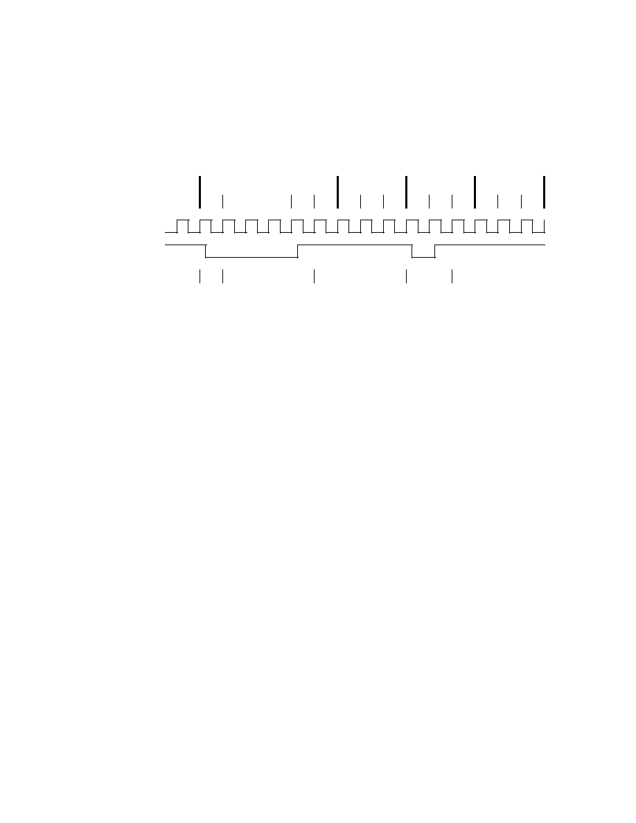
108
SERIAL IRQ
The FDC37M60x will support the serial interrupt
to transmit interrupt information to the host
system. The serial interrupt scheme adheres to
the Serial IRQ Specification for PCI Systems,
Version 6.0.
Timing Diagrams For IRQSER Cycle
PCICLK = 33 MHz_IN pin
IRQSER = SIRQ pin
A) Start Frame timing with source sampled a low pulse on IRQ1
R
T
S
R
T
S
IRQSER
PCICLK
Host Controller
IRQ1
IRQ1
Drive Source
R
T
None
IRQ0 FRAME IRQ1 FRAME
S
R
T
IRQ2 FRAME
None
START
START FRAME
H
SL
or
H
1
H=Host Control, R=Recovery, SL=Slave Control, T=Turn-Around, S=Sample
1) Start Frame pulse can be 4-8 clocks wide.

109
B) Stop Frame Timing with Host using 17 IRQSER sampling period
S
R
T
S
IRQSER
PCICLK
Host Controller
IRQ15
Driver
R
T
None
IRQ14
IRQ15
S
R
T
IOCHCK#
None
STOP
R
T
STOP FRAME
H
I
START
NEXT CYCLE
1
2
3
FRAME
FRAME
FRAME
H=Host Control, R=Recovery, I=Idle, T=Turn-Around, S=Sample
1)
Stop pulse is 2 clocks wide for Quiet mode, 3 clocks wide for Continuous mode.
2)
There may be none, one or more Idle states during the Stop Frame.
3)
The next IRQSER cycle's Start Frame pulse may or may not start immediately
after the turn-around clock of the Stop Frame.

110
IRQSER Cycle Control
There are two modes of operation for the
IRQSER Start Frame.
1) Quiet (Active) Mode: Any device may initiate
a Start Frame by driving the IRQSER low for
one clock, while the IRQSER is Idle. After
driving low for one clock the IRQSER must
immediately be tri-stated without at any time
driving high. A Start Frame may not be initiated
while the IRQSER is Active. The IRQSER is Idle
between Stop and Start Frames. The IRQSER
is Active between Start and Stop Frames. This
mode of operation allows the IRQSER to be Idle
when there are no IRQ/Data transitions which
should be most of the time.
Once a Start Frame has been initiated the Host
Controller will take over driving the IRQSER low
in the next clock and will continue driving the
IRQSER low for a programmable period of three
to seven clocks. This makes a total low pulse
width of four to eight clocks. Finally, the Host
Controller will drive the IRQSER back high for
one clock, then tri-state.
Any IRQSER Device (i.e., The FDC37M60x)
which detects any transition on an IRQ/Data line
for which it is responsible must initiate a Start
Frame in order to update the Host Controller
unless the IRQSER is already in an IRQSER
Cycle and the IRQ/Data transition can be
delivered in that IRQSER Cycle.
2) Continuous (Idle) Mode: Only the Host
controller can initiate a Start Frame to update
IRQ/Data line information. All other IRQSER
agents become passive and may not initiate a
Start Frame. IRQSER will be driven low for four
to eight clocks by Host Controller. This mode
has two functions. It can be used to stop or idle
the IRQSER or the Host Controller can operate
IRQSER in a continuous mode by initiating a
Start Frame at the end of every Stop Frame.
An IRQSER mode transition can only occur
during the Stop Frame. Upon reset, IRQSER
bus is defaulted to Continuous mode,
therefore only the Host controller can initiate
the first Start Frame. Slaves must
continuously sample the Stop Frames pulse
width to determine the next IRQSER Cycle's
mode.
IRQSER Data Frame
Once a Start Frame has been initiated, the
FDC37M60x will watch for the rising edge of the
Start Pulse and start counting IRQ/Data Frames
from there. Each IRQ/Data Frame is three
clocks: Sample phase, Recovery phase, and
Turn-around phase. During the Sample phase
the FDC37M60x must drive the IRQSER (SIRQ
pin) low, if and only if, its last detected IRQ/Data
value was low. If its detected IRQ/Data value is
high, IRQSER must be left tri-stated. During the
Recovery phase the FDC37M60x must drive the
SERIRQ high, if and only if, it had driven the
IRQSER low during the previous Sample Phase.
During the Turn-around Phase the FDC37M60x
must tri-state the SERIRQ. The FDC37M60x will
drive the IRQSER line low at the appropriate
sample point if its associated IRQ/Data line is
low, regardless of which device initiated the
Start Frame.
The Sample Phase for each IRQ/Data follows
the low to high transition of the Start Frame
pulse by a number of clocks equal to the
IRQ/Data Frame times three, minus one. (e.g.
The IRQ5 Sample clock is the sixth IRQ/Data
Frame, (6 x 3) - 1 = 17th clock after the rising
edge of the Start Pulse.)

111
Table 47 - IRQSER Sampling Periods
IRQSER PERIOD
SIGNAL SAMPLED
NUMBER OF CLOCKS PAST START
1
Not Used
2
2
IRQ1
5
3
IRQ2
8
4
IRQ3
11
5
IRQ4
14
6
IRQ5
17
7
IRQ6
20
8
IRQ7
23
9
IRQ8
26
10
IRQ9
29
11
IRQ10
32
12
IRQ11
35
13
IRQ12
38
14
IRQ13
41
15
IRQ14
44
16
IRQ15
47
Note:
The SIRQ data frame will now support IRQ2 from a logical device, previously IRQSER Period
3 was reserved for use by the System Management Interrupt (nSMI). The FDC37M60x does not
support SMI.
IRQSER Period 14 is used to transfer IRQ13. Logical devices 0 (FDC), 3 (Par Port), 4 (Ser Port 1), 5
(Ser Port 2), 6 (RTC), and 7 (KBD) shall have IRQ13 as a choice for their primary interrupt.

112
Stop Cycle Control
Once all IRQ/Data Frames have completed the
Host Controller will terminate IRQSER activity
by initiating a Stop Frame. Only the Host
Controller can initiate the Stop Frame. A Stop
Frame is indicated when the IRQSER is low for
two or three clocks. If the Stop Frame's low
time is two clocks then the next IRQSER Cycle's
sampled mode is the Quiet mode; and any
IRQSER device may initiate a Start Frame in
the second clock or more after the rising edge
of the Stop Frame's pulse. If the Stop Frame's
low time is three clocks then the next IRQSER
Cycle's sampled mode is the Continuos mode;
and only the Host Controller may initiate a Start
Frame in the second clock or more after the
rising edge of the Stop Frame's pulse.
Latency
Latency for IRQ/Data updates over the IRQSER
bus in bridge-less systems with the minimum
IRQ/Data Frames of seventeen, will range up to
96 clocks (3.84
µ
S with a 25 MHz PCI Bus or
2.88
µ
S with a 33 MHz PCI Bus). If one or more
PCI to PCI Bridge is added to a system, the
latency for IRQ/Data updates from the
secondary or tertiary buses will be a few clocks
longer for synchronous buses, and
approximately double for asynchronous buses.
EOI/ISR Read Latency
Any serialized IRQ scheme has a potential
implementation issue related to IRQ latency.
IRQ latency could cause an EOI or ISR Read to
precede an IRQ transition that it should have
followed. This could cause a system fault. The
host interrupt controller is responsible for
ensuring that these latency issues are mitigated.
The recommended solution is to delay EOIs and
ISR Reads to the interrupt controller by the
same amount as the IRQSER Cycle latency in
order to ensure that these events do not occur
out of order.
AC/DC Specification Issue
All IRQSER agents must drive / sample
IRQSER synchronously related to the rising
edge of PCI bus clock. IRQSER (SIRQ) pin
uses the electrical specification of PCI bus.
Electrical parameters will follow PCI
specification, section 4, sustained tri-state.
Reset and Initialization
The IRQSER bus uses RESET_DRV as its reset
signal. The IRQSER pin is tri-stated by all
agents while RESET_DRV is active. With reset,
IRQSER Slaves are put into the (continuous)
IDLE mode. The Host Controller is responsible
for starting the initial IRQSER Cycle to collect
system's IRQ/Data default values. The system
then follows with the Continuous/Quiet mode
protocol (Stop Frame pulse width) for
subsequent IRQSER Cycles. It is Host
Controller's responsibility to provide the default
values to 8259's and other system logic before
the first IRQSER Cycle is performed. For
IRQSER system suspend, insertion, or removal
application, the Host controller should be
programmed into Continuous (IDLE) mode first.
This is to guarantee IRQSER bus is in IDLE
state before the system configuration changes.
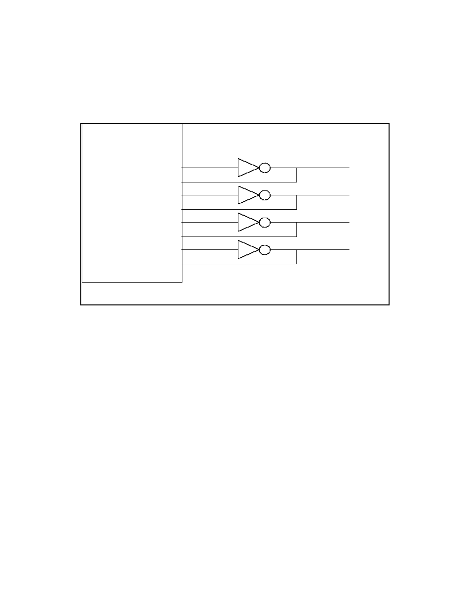
113
8042 KEYBOARD CONTROLLER DESCRIPTION
The FDC37M60x is a Super I/O and Universal
Keyboard Controller that is designed for
intelligent keyboard management in desktop
computer applications. The Super I/O supports
a Floppy Disk Controller, two 16550 type serial
ports one ECP/EPP Parallel Port.
The Universal Keyboard Controller uses an
8042 microcontroller CPU core. This section
concentrates on the FDC37M60x enhancements
to the 8042. For general information about the
8042, refer to the "Hardware Description of the
8042" in the 8 Bit Embedded Controller Hand-
book.
KIRQ is the Keyboard IRQ
MIRQ is the Mouse IRQ
Port 21 is used to create a GATEA20 signal from the FDC37M60x.
8042A
P27
P10
P26
TST0
P23
TST1
P22
P11
KDAT
KCLK
MCLK
MDAT
Keyboard and Mouse Interface
LS05

114
KEYBOARD ISA INTERFACE
The FDC37M60x ISA interface is functionally
compatible with the 8042 style host interface. It
consists of the D0-7 data bus; the nIOR, nIOW
and the Status register, Input Data
register, and Output Data register. Table 48
shows how the interface decodes the control
signals. In addition to the above signals, the
host interface includes keyboard and mouse
IRQs.
Table 48 - ISA I/O Address Map
ISA ADDRESS
nIOW
nIOR
BLOCK
FUNCTION (NOTE 1)
0x60
0
1
KDATA
Keyboard Data Write (C/D=0)
1
0
KDATA
Keyboard Data Read
0x64
0
1
KDCTL
Keyboard Command Write (C/D=1)
1
0
KDCTL
Keyboard Status Read
Note 1: These registers consist of three separate 8 bit registers. Status, Data/Command Write and
Data Read.
Keyboard Data Write
This is an 8 bit write only register. When
written, the C/D status bit of the status register
is cleared to zero and the IBF bit is set.
Keyboard Data Read
This is an 8 bit read only register. If enabled by
"ENABLE FLAGS", when read, the KIRQ output
is cleared and the OBF flag in the status register
is cleared. If not enabled, the KIRQ and/or
AUXOBF1 must be cleared in software.
Keyboard Command Write
This is an 8 bit write only register. When
written, the C/D status bit of the status register
is set to one and the IBF bit is set.
Keyboard Status Read
This is an 8 bit read only register. Refer to the
description of the Status Register for more
information.

115
CPU-to-Host Communication
The FDC37M60x CPU can write to the Output
Data register via register DBB. A write
to this register automatically sets Bit 0 (OBF) in
the Status register. See Table 49.
Table 49 - Host Interface Flags
8042 INSTRUCTION
FLAG
OUT DBB
Set OBF, and, if enabled, the KIRQ output signal goes high
Host-to-CPU Communication
The host system can send both commands and
data to the Input Data register. The CPU
differentiates between commands and data by
reading the value of Bit 3 of the Status register.
When bit 3 is "1", the CPU interprets the register
contents as a command. When bit 3 is "0", the
CPU interprets the register contents as data.
During a host write operation, bit 3 is set to "1" if
SA2 = 1 or reset to "0" if SA2 = 0.
KIRQ
If "EN FLAGS" has been executed and P24 is
set to a one: the OBF flag is gated onto KIRQ.
The KIRQ signal can be connected to system
interrupt to signify that the FDC37M60x CPU
has written to the output data register via "OUT
DBB,A". If P24 is set to a zero, KIRQ is forced
low. On power-up, after a valid RST pulse has
been delivered to the device, KIRQ is reset to 0.
KIRQ will normally reflects the status of writes
"DBB". (KIRQ is normally selected as IRQ1 for
keyboard support.)
If "EN FLAGS" has not been executed: KIRQ
can be controlled by writing to P24. Writing a
zero to P24 forces KIRQ low; a high forces
KIRQ high.
MIRQ
If "EN FLAGS" has been executed and P25 is
set to a one:; IBF is inverted and gated onto
MIRQ. The MIRQ signal can be connected to
system interrupt to signify that the FDC37M60x
CPU has read the DBB register.
If "EN FLAGS" has not been executed, MIRQ is
controlled by P25, Writing a zero to P25 forces
MIRQ low, a high forces MIRQ high. (MIRQ is
normally selected as IRQ12 for mouse support.)
Gate A20
A general purpose P21 is used as a software
controlled Gate A20 or user defined output.
EXTERNAL KEYBOARD AND MOUSE
INTERFACE
Industry-standard PC-AT-compatible keyboards
employ a two-wire, bidirectional TTL interface
for data transmission. Several sources also
supply PS/2 mouse products that employ the
same type of interface. To facilitate system
expansion, the FDC37M60x provides four signal
pins that may be used to implement this
interface directly for an external keyboard and
mouse.

116
The FDC37M60x has four high-drive, open-drain
output, bidirectional port pins that can be used
for external serial interfaces, such as ISA
external keyboard and PS/2-type mouse
interfaces. They are KCLK, KDAT, MCLK, and
MDAT. P26 is inverted and output as KCLK. The
KCLK pin is connected to TEST0. P27 is
inverted and output as KDAT. The KDAT pin is
connected to P10. P23 is inverted and output as
MCLK. The MCLK pin is connected to TEST1.
P22 is inverted and output as MDAT. The MDAT
pin is connected to P11. Note: External pull-ups
may be required.
KEYBOARD POWER MANAGEMENT
The keyboard provides support for two power-
saving modes: soft powerdown mode and hard
powerdown mode. In soft powerdown mode,
the clock to the ALU is stopped but the
timer/counter and interrupts are still active. In
hard power down mode the clock to the 8042 is
stopped.
Soft Power Down Mode
This mode is entered by executing a HALT
instruction. The execution of program code is
halted until either RESET is driven active or a
data byte is written to the DBBIN register by a
master CPU. If this mode is exited using the
interrupt, and the IBF interrupt is enabled, then
program execution resumes with a CALL to the
interrupt routine, otherwise the next instruction
is executed. If it is exited using RESET then a
normal reset sequence is initiated and program
execution starts from program memory location
0.
Hard Power Down Mode
This mode is entered by executing a STOP
instruction. The oscillator is stopped by
disabling the oscillator driver cell. When
either RESET is driven active or a data byte is
written to the DBBIN register by a master
CPU, this mode will be exited (as above).
However, as the oscillator cell will require an
initialization time, either RESET must be held
active for sufficient time to allow the oscillator to
stabilise. Program execution will resume as
above.
INTERRUPTS
The FDC37M60x provides the two 8042
interrupts. IBF and the Timer/Counter Overflow.
MEMORY CONFIGURATIONS
The FDC37M60x provides 2K of on-chip ROM
and 256 bytes of on-chip RAM.
Register Definitions
Host I/F Data Register
The Input Data register and Output Data register
are each 8 bits wide. A write to this 8 bit register
will load the Keyboard Data Read Buffer, set the
OBF flag and set the KIRQ output if enabled. A
read of this register will read the data from the
Keyboard Data or Command Write Buffer and
clear the IBF flag. Refer to the KIRQ and Status
register descriptions for more information.
Host I/F Status Register
The Status register is 8 bits wide. Table 50
shows the contents of the Status register.

117
Table 50 - Status Register
D7
D6
D5
D4
D3
D2
D1
D0
UD
UD
UD
UD
C/D
UD
IBF
OBF
Status Register
This register is cleared on a reset. This register
is read-only for the Host and read/write by the
FDC37M60x CPU.
UD Writable by FDC37M60x CPU. These bits
are user-definable.
C/D (Command Data) - This bit specifies
whether the input data register contains data or
a command (0 = data, 1 = command). During a
host data/command write operation, this bit is
set to "1" if SA2 = 1 or reset to "0" if SA2 = 0.
IBF (Input Buffer Full) - This flag is set to "1"
whenever the host system writes data into the
input data register. Setting this flag activates
the FDC37M60x CPU's nIBF (MIRQ) interrupt if
enabled. When the FDC37M60x CPU reads the
input data register (DBB), this bit is
automatically reset and the interrupt is
cleared. There is no output pin associated with
this internal signal.
OBF
(Output Buffer Full) - This flag is set to
whenever the FDC37M60x CPU write to the
output data register (DBB). When the host
system reads the output data register, this bit is
automatically reset.
EXTERNAL CLOCK SIGNAL
The FDC37M60x Keyboard Controller clock
source is a 12 MHz clock generated from a
14.318 MHz clock. The reset pulse must last for
at least 24 16 MHz clock periods. The pulse-
width requirement applies to both internally (Vcc
POR) and externally generated reset signals. In
powerdown mode, the external clock signal is
not loaded by the chip.
DEFAULT RESET CONDITIONS
The FDC37M60x has one source of reset: an
external reset via the RESET_DRV pin. Refer to
Table 51 for the effect of each type of reset on
the internal registers.
Table 51 - Resets
DESCRIPTION
HARDWARE RESET (RESET)
KCLK
Weak High
KDAT
Weak High
MCLK
Weak High
MDAT
Weak High
Host I/F Data Reg
N/A
Host I/F Status Reg
00H
N/A: Not Applicable

118
GATEA20 AND KEYBOARD RESET
The FDC37M60x provides two options for
GateA20 and Keyboard Reset: 8042 Software
Generated GateA20 and KRESET and Port 92
Fast GateA20 and KRESET.
PORT 92 FAST GATEA20 AND KEYBOARD
RESET
Port 92 Register
This port can only be read or written if Port 92
has been enabled via bit 2 of the KRST_GA20
Register (Logical Device 7, 0xF0) set to 1.
This register is used to support the alternate
reset (nALT_RST) and alternate A20 (ALT_A20)
functions.
Name
Port 92
Location
92h
Default Value
24h
Attribute
Read/Write
Size
8 bits
Port 92 Register
Bit
Function
7:6
Reserved. Returns 00 when read.
5
Reserved. Returns a 1 when read.
4
Reserved. Returns a 0 when read.
3
Reserved. Returns a 0 when read.
2
Reserved. Returns a 1 when read.
1
ALT_A20 Signal control. Writing a 0 to this bit causes the ALT_A20 signal to be
driven low. Writing a 1 to this bit causes the ALT_A20 signal to be driven high.
0
Alternate System Reset. This read/write bit provides an alternate system reset
function. This function provides an alternate means to reset the system CPU to
effect a mode switch from Protected Virtual Address Mode to the Real Address
Mode. This provides a faster means of reset than is provided by the Keyboard
controller. This bit is set to a 0 by a system reset. Writing a 1 to this bit will cause
the nALT_RST signal to pulse acitive (low) for a minimum of 1 µs after a delay of
500 ns. Before another nALT_RST pulse can be generated, this bit must be
written back to a 0.
nGATEA20
8042 P21
ALT_A20
System nA20M
0
0
0
0
1
1
1
0
1
1
1
1
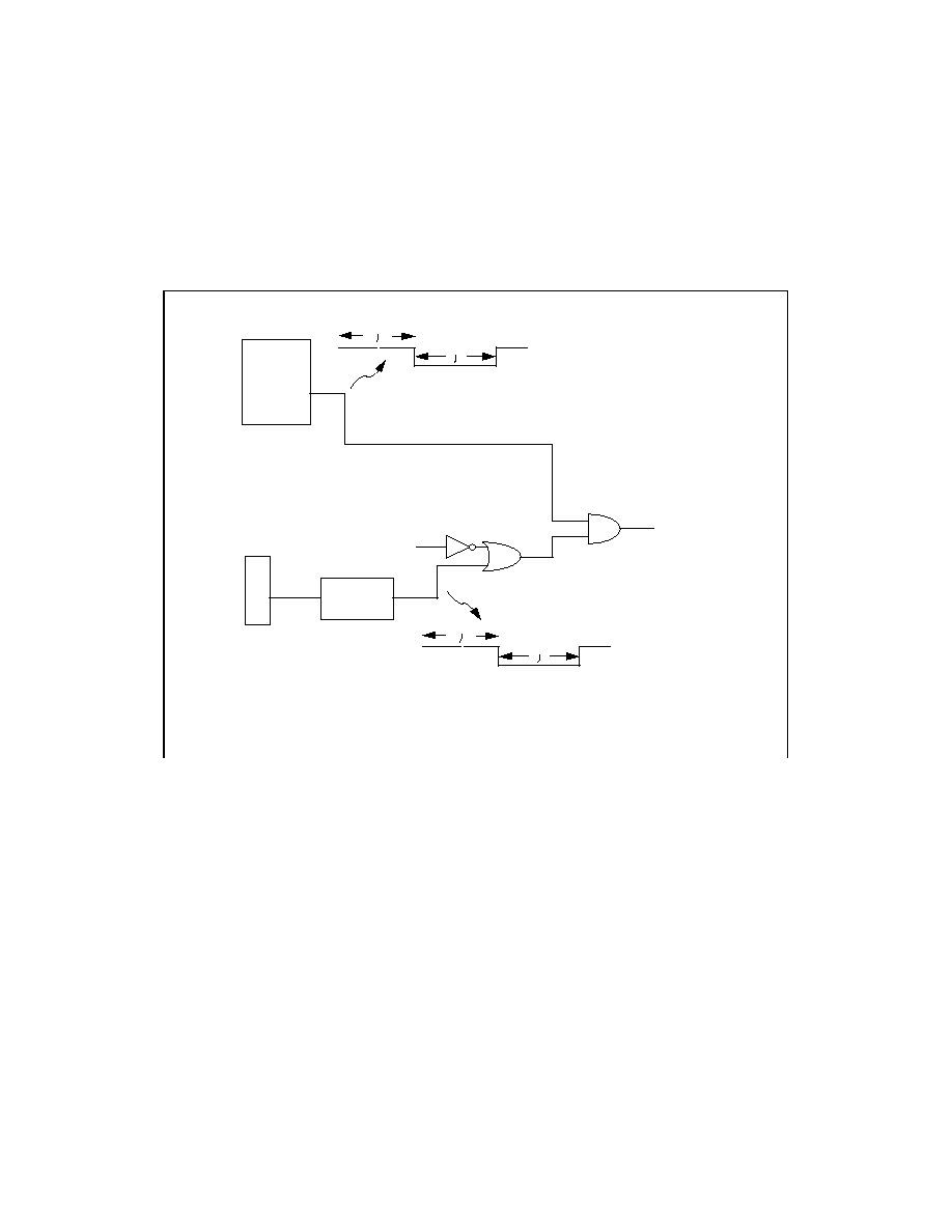
119
Bit 0 of Port 92, which generates the nALT_RST
signal, is used to reset the CPU under program
control. This signal is AND'ed together
externally with the reset signal (nKBDRST) from
the keyboard controller to provide a software
means of resetting the CPU. This provides a
faster means of reset than is provided by the
keyboard controller. Writing a 1 to bit 0 in the
Port 92 Register causes this signal to pulse low
for a minimum of 6µs, after a delay of a
minimum of 14µs. Before another nALT_RST
pulse can be generated, bit 0 must be set to 0
either by a system reset of a write to Port 92.
Upon reset, this signal is driven inactive high (bit
0 in the Port 92 Register is set to 0).
If Port 92 is enabled, i.e., bit 2 of KRST_GA20 is
set to 1, then a pulse is generated by writing a 1
to bit 0 of the Port 92 Register and this pulse is
AND'ed with the pulse generated from the 8042.
This pulse is output on pin KRESET and its
polarity is controlled by the GPI/O polarity
configuration.
8042
P92
Pulse
Gen
KBDRST
KRST_GA20
Bit 2
Bit 0
P20
KRST
nALT_RST
6us
14us
~ ~
6us
14us
~ ~
Note: When Port 92 is disabled,
writes are ignored and reads
return undefined values.
KRESET Generation

120
Bit 1 of Port 92, the ALT_A20 signal, is used to
force nA20M to the CPU low for support of real
mode compatible software. This signal is
externally OR'ed with the A20GATE signal from
the keyboard controller and CPURST to control
the nA20M input of the CPU. Writing a 0 to bit 1
of the Port 92 Register forces ALT_A20 low.
ALT_A20 low drives nA20M to the CPU low, if
A20GATE from the keyboard controller is also
low. Writing a 1 to bit 1 of the Port 92 Register
forces ALT_A20 high. ALT_A20 high drives
nA20M to the CPU high, regardless of the state
of A20GATE from the keyboard controller. Upon
reset, this signal is driven low.
8042 P12 and P16 Functions
8042 functions P12 and P16 are implemented
as in a true 8042 part. Reference the 8042 spec
for all timing. A port signal of 0 drives the
output to 0. A port signal of 1 causes the port
enable signal to drive the output to 1 within 20-
30nsec. After several (# TBD) clocks, the port
enable goes away and the internal 90µA pull-up
maintains the output signal as 1.
In 8042 mode, the pins can be programmed as
open drain. When programmed in open drain
mode, the port enables do not come into play. If
the port signal is 0 the output will be 0. If the
port signal is 1, the output tristates: an external
pull-up can pull the pin high. In 8042 mode, the
pins cannot be programmed as input nor
inverted through the GP configuration registers.

121
0ns
250ns
500ns
CLK
AEN
nAEN
64=I/O Addr
n64
nIOW
nA
DD1
nDD1
nCNTL
nIOW'
nIOW+n64
AfterD1
nAfterD1
60=I/O Addr
n60
nIOW+n60=B
nAfterD1+B
D[1]
GA20
Gate A20 Turn-On Sequence Timing
When writing to the command and data port
with hardware speedup, the IOW timing shown
in the figure titled "IOW Timing for Port 92" in
the Timing Diagrams Section is used. This
setup time is only required to be met when using
hardware speedup; the data must be valid a
minimum of 0 nsec from the leading edge of
the write and held throughout the entire write
cycle.

122
CONFIGURATION
The Configuration of the FDC37M60x is very
flexible and is based on the configuration
architecture implemented in typical Plug-and-
Play components. The FDC37M60x is designed
for motherboard applications in which the
resources required by their components are
known. With its flexible resource allocation
architecture, the FDC37M60x allows the BIOS to
assign resources at POST.
SYSTEM ELEMENTS
Primary Configuration Address Decoder
After a hard reset (RESET_DRV pin asserted) or
Vcc Power On Reset the FDC37M60x is in the
Run Mode with all logical devices disabled. The
logical devices may be configured through two
standard Configuration I/O Ports (INDEX and
DATA) by placing the FDC37M60x into
Configuration Mode. The BIOS uses these
configuration ports to initialize the logical
devices at POST. The INDEX and DATA ports
are only valid when the FDC37M60x is in
Configuration Mode.
The SYSOPT pin is latched on the falling edge
of the RESET_DRV or on Vcc Power On Reset
to determine the configuration register's base
address. The SYSOPT pin is used to select the
CONFIG PORT's I/O address at power-up.
Once powered up the configuration port base
address can be changed through configuration
registers CR26 and CR27. The SYSOPT pin
is a hardware configuration pin which is
shared with the nRTS1 signal on pin 87.
During reset this pin is a weak active low signal
which sinks 30µA. Note: All I/O addresses are
qualified with AEN.
The INDEX and DATA ports are effective only
when the chip is in the Configuration State.
PORT NAME
SYSOPT= 0
(PULL-DOWN RESISTOR)
REFER TO NOTE 1
SYSOPT= 1
(10K PULL-UP
RESISTOR)
TYPE
CONFIG PORT (
Note 2)
0x03F0
0x0370
Write
INDEX PORT (
Note 2)
0x03F0
0x0370
Read/Write
DATA PORT
INDEX PORT + 1
Read/Write
Note 1: If using TTL RS232 drivers use 1K pull-down. If using CMOS RS232 drivers use 10K
pull-down.
Note 2: The configuration port base address can be relocated through CR26 and CR27.
Entering the Configuration State
The device enters the Configuration State when
the following Config Key is successfully written
to the CONFIG PORT.
Config Key = < 0x55 >
Exiting the Configuration State
The device exits the Configuration State when
the following Config Key is successfully written
to the CONFIG PORT.
Config Key = < 0xAA>

123
CONFIGURATION SEQUENCE
To program the configuration registers, the
following sequence must be followed:
1. Enter Configuration Mode
2. Configure the Configuration Registers
3. Exit Configuration Mode.
Enter Configuration Mode
To place the chip into the
Configuration State the Config Key is sent to
the chip's CONFIG PORT. The config key
consists of 0x55 written to the CONFIG PORT.
Once the configuration key is received
correctly the chip enters into the Configuration
State (The auto Config ports are enabled).
Configuration Mode
The system sets the logical device information
and activates desired logical devices through
the INDEX and DATA ports. In configuration
mode, the INDEX PORT is located at the
CONFIG PORT address and the DATA PORT
is at INDEX PORT address + 1.
The desired configuration registers are
accessed in two steps:
a. Write the index of the Logical Device
Number Configuration Register (i.e., 0x07)
to the INDEX PORT and then write the
number of the desired logical device to the
DATA PORT
b. Write the address of the desired
configuration register within the logical
device to the INDEX PORT and then write
or read the configuration register through
the DATA PORT.
Note: if accessing the Global Configuration
Registers, step (a) is not required.
Exit Configuration Mode
To exit the Configuration State the system
writes 0xAA to the CONFIG PORT. The chip
returns to the RUN State.
Note: Only two states are defined (Run and
Configuration). In the Run State the chip will
always be ready to enter the Configuration
State.
Programming Example
The following is an example of a configuration
program in Intel 8086 assembly language.
;----------------------------.
; ENTER CONFIGURATION MODE |
;----------------------------'
MOV DX,3F0H
MOV AX,055H
OUT DX,AL
;----------------------------.
; CONFIGURE REGISTER CRE0, |
; LOGICAL DEVICE 8 |
;----------------------------'
MOV DX,3F0H
MOV AL,07H
OUT DX,AL ; Point to nLD Config Reg
MOV DX,3F1H
MOV AL, 08H
OUT DX,AL; Point to Logical Device
8
;
MOV DX,3F0H
MOV AL,E0H
OUT DX,AL
; Point to CRE0
MOV DX,3F1H
MOV AL,02H
OUT DX,AL
; Update CRE0
;----------------------------.
; EXIT CONFIGURATION MODE |
;----------------------------'
MOV DX,3F0H
MOV AX,0AAH
OUT DX,AL

124
Notes: 1. HARD RESET: RESET_DRV pin asserted
2. SOFT RESET: Bit 0 of Configuration Control register set to one
3. All host accesses are blocked for 500µs after Vcc POR (see Power-up Timing Diagram)
Table 52 - Configuration Registers
INDEX
TYPE
HARD RESET
Vcc
POR
SOFT
RESET
CONFIGURATION REGISTER
GLOBAL CONFIGURATION REGISTERS
0x02
W
0x00
-
-
Config Control
0x07
R/W
0x00
-
0x00
Logical Device Number
0x20
R
0x47
Device ID - hard wired
0x21
R
Current Revision
Device Rev - hard wired
0x22
R/W
0x00
-
0x00
Power Control
0x23
R/W
0x00
-
-
Power Mgmt
0x24
R/W
0x04
-
-
OSC
0x26
R/W
Sysopt=0: 0xF0
Sysopt=1: 0x70
-
-
Configuration Port Address Byte 0
0x27
R/W
Sysopt=0: 0x03
Sysopt=1: 0x03
-
-
Configuration Port Address Byte 1
0x2B
R/W
-
0x00
-
TEST 4
0x2C
R/W
-
0x00
-
TEST 5
0x2D
R/W
-
0x00
-
TEST 1
0x2E
R/W
-
0x00
-
TEST 2
0x2F
R/W
-
0x00
-
TEST 3
LOGICAL DEVICE 0 CONFIGURATION REGISTERS (FDD)
0x30
R/W
0x00
-
0x00
Activate
0x60,
0x61
R/W
0x03,
0xF0
-
0x03,0
xF0
Primary Base I/O Address
0x70
R/W
0x06
-
0x06
Primary Interrupt Select
0x74
R/W
0x02
-
0x02
DMA Channel Select
0xF0
R/W
0x0E
-
-
FDD Mode Register
0xF1
R/W
0x00
-
-
FDD Option Register
0xF2
R/W
0xFF
-
-
FDD Type Register
0xF4
R/W
0x00
-
-
FDD0
0xF5
R/W
0x00
-
-
FDD1

125
Table 52 - Configuration Registers
INDEX
TYPE
HARD RESET
Vcc
POR
SOFT
RESET
CONFIGURATION REGISTER
LOGICAL DEVICE 1 CONFIGURATION REGISTERS (RESERVED)
LOGICAL DEVICE 2 CONFIGURATION REGISTERS (RESERVED)
LOGICAL DEVICE 3 CONFIGURATION REGISTERS (Parallel Port)
0x30
R/W
0x00
-
0x00
Activate
0x60,
0x61
R/W
0x00,
0x00
-
0x00,0
x00
Primary Base I/O Address
0x70
R/W
0x00
-
0x00
Primary Interrupt Select
0x74
R/W
0x04
-
0x04
DMA Channel Select
0xF0
R/W
0x3C
-
-
Parallel Port Mode Register
0xF1
R/W
0x00
-
-
Parallel Port Mode Register 2
LOGICAL DEVICE 4 CONFIGURATION REGISTERS (Serial Port 1)
0x30
R/W
0x00
-
0x00
Activate
0x60,
0x61
R/W
0x00,
0x00
-
0x00,0
x00
Primary Base I/O Address
0x70
R/W
0x00
-
0x00
Primary Interrupt Select
0xF0
R/W
0x00
-
-
Serial Port 1 Mode Register
LOGICAL DEVICE 5 CONFIGURATION REGISTERS (Serial Port 2)
0x30
R/W
0x00
-
0x00
Activate
0x60,
0x61
R/W
0x00,
0x00
-
0x00,0
x00
Primary Base I/O Address
0x70
R/W
0x00
-
0x00
Primary Interrupt Select
0x74
R/W
0x04
-
0x04
DMA Channel Select
0xF0
R/W
0x00
-
-
Serial Port 2 Mode Register
0xF1
R/W
0x02
-
-
IR Options Register
0xF2
R/W
0x03
-
-
IR Half Duplex Timeout
LOGICAL DEVICE 6 CONFIGURATION REGISTERS (RESERVED)
LOGICAL DEVICE 7 CONFIGURATION REGISTERS (Keyboard)
0x30
R/W
0x00
-
0x00
Activate
0x70
R/W
0x00
-
0x00
Primary Interrupt Select
0x72
R/W
0x00
-
0x00
Second Interrupt Select
0xF0
R/W
0x00
-
KRESET and GateA20 Select

126
Table 52 - Configuration Registers
INDEX
TYPE
HARD RESET
Vcc
POR
SOFT
RESET
CONFIGURATION REGISTER
LOGICAL DEVICE 8 CONFIGURATION REGISTERS (Aux I/O)
0x30
R/W
0x00
-
0x00
Activate
0xC0
R/W
0x06
-
-
Pin Multiplex Controls
0xC1
R/W
0x03
-
-
Force Disk Change
0xC2
R
-
-
-
Floppy Data Rate Select Shadow
0xC3
R
-
-
-
UART1 FIFO Control Shadow
0xC4
R
-
-
-
UART2 FIFO Control Shadow
0xF6:
FB
-
-
-
Reserved
LOGICAL DEVICE 9 CONFIGURATION REGISTERS (RESERVED)
Note1: This register contains some bits which are read or write only.

127
Chip Level (Global) Control/Configuration
Registers[0x00-0x2F]
The chip-level (global) registers lie in the
address range [0x00-0x2F]. The design MUST
use all 8 bits of the ADDRESS Port for register
selection. All unimplemented registers and bits
ignore writes and return zero when read.
The INDEX PORT is used to select a
configuration register in the chip. The DATA
PORT is then used to access the selected
register. These registers are accessable only in
the Configuration Mode.
Table 53 - Chip Level Registers
REGISTER
ADDRESS
DESCRIPTION
STATE
Chip (Global) Control Registers
0x00 -
0x01
Reserved - Writes are ignored, reads return 0.
Config Control
Default = 0x00
on Vcc POR or
Reset_Drv
0x02 W
The hardware automatically clears this bit after the
write, there is no need for software to clear the bits.
Bit 0 = 1: Soft Reset. Refer to the "Configuration
Registers" table for the soft reset value for each
register.
C
0x03 - 0x06
Reserved - Writes are ignored, reads return 0.
Logical Device #
Default = 0x00
on Vcc POR or
Reset_Drv
0x07 R/W
A write to this register selects the current logical
device. This allows access to the control and
configuration registers for each logical device.
Note: the Activate command operates only on the
selected logical device.
C
Card Level
Reserved
0x08 - 0x1F
Reserved - Writes are ignored, reads return 0.
Chip Level, SMSC Defined
Device ID
Hard wired
= 0x47
0x20 R
A read only register which provides device
identification. Bits[7:0] = 0x47 when read.
C
Device Rev
Hard wired
= Current Revision
0x21 R
A read only register which provides device revision
information. Bits[7:0] = 0x00 when read.
C

128
Table 53 - Chip Level Registers
REGISTER
ADDRESS
DESCRIPTION
STATE
PowerControl
Default = 0x00.
on Vcc POR or
Reset_Drv hardware
signal
0x22 R/W
Bit[0] FDC Power
Bit[1] Reserved
Bit[2] Reserved
Bit[3] Parallel Port Power
Bit[4] Serial Port 1 Power
Bit[5] Serial Port 2 Power
Bit[6] Reserved
Bit[7] Reserved (read as 0)
= 0 Power off or disabled
= 1 Power on or enabled
C
Power Mgmt
Default = 0x00.
on Vcc POR or
Reset_Drv hardware
signal
0x23 R/W
Bit[0] FDC
Bit[1] Reserved
Bit[2] Reserved
Bit[3] Parallel Port
Bit[4] Serial Port 1
Bit[5] Serial Port 2
Bit[6:7] Reserved (read as 0)
= 0 Intelligent Pwr Mgmt off
= 1 Intelligent Pwr Mgmt on
C

129
Table 54 - Chip Level Registers
REGISTER
ADDRESS
DESCRIPTION
STATE
OSC
Default = 0x04, on
Vcc POR or
Reset_Drv hardware
signal.
0x24 R/W
Bit[0] Reserved
Bit [1] PLL Control
= 0 PLL is on (backward Compatible)
= 1 PLL is off
Bits[3:2] OSC
= 01
Osc is on, BRG clock is on.
= 10
Same as above (01) case.
= 00
Osc is on, BRG Clock Enabled.
= 11
Osc is off, BRG clock is disabled.
Bit [5:4] Reserved, set to zero
Bit [6] 16-Bit Address Qualification
= 0 12-Bit Address Qualification
= 1 16-Bit Address Qualification
Bit[7] Reserved
C
Chip Level
Vendor Defined
0x25
Reserved - Writes are ignored, reads return 0.
Configuration
Address Byte 0
Default
=0
x
F0 (Sysopt=0)
=0
x
70 (Sysopt=1)
on Vcc POR or
Reset_Drv
0x26
Bit[7:1] Configuration Address Bits [7:1]
Bit[0] = 0
See Note 1
C
Configuration
Address Byte 1
Default = 0x03
on Vcc POR or
Reset_Drv
0x27
Bit[7:0] Configuration Address Bits [15:8]
See Note 1
C
Default = 0x00
on VCC POR and
Hard Reset
0x28
Bits[7:0] Reserved - Writes are ignored, reads
return 0.
Chip Level
Vendor Defined
0x29 -0x2A
Reserved - Writes are ignored, reads return 0.

130
Table 54 - Chip Level Registers
REGISTER
ADDRESS
DESCRIPTION
STATE
TEST 4
Default = 0x00, on
Vcc POR
0x2B R/W
Test Modes: Reserved for SMSC. Users should not
write to this register, may produce undesired
results.
C
TEST 5
Default = 0x00, on
Vcc POR
0x2C R/W
Test Modes: Reserved for SMSC. Users should not
write to this register, may produce undesired
results.
C
TEST 1
Default = 0x00, on
Vcc POR
0x2D R/W
Test Modes: Reserved for SMSC. Users should not
write to this register, may produce undesired
results.
C
TEST 2
Default = 0x00, on
Vcc POR
0x2E R/W
Test Modes: Reserved for SMSC. Users should not
write to this register, may produce undesired
results.
C
TEST 3
Default = 0x00, on
Vcc POR
0x2F R/W
Test Modes: Reserved for SMSC. Users should not
write to this register, may produce undesired
results.
C
Note 1: To allow the selection of the configuration address to a user defined location, these
Configuration Address Bytes are used. There is no restriction on the address chosen, except that A0
is 0, that is, the address must be on an even byte boundary. As soon as both bytes are changed, the
configuration space is moved to the specified location with no delay (Note: Write byte 0, then byte 1;
writing CR27 changes the base address).
The configuration address is only reset to its default address upon a Hard Reset or Vcc POR.
Note: The default configuration address is either 3F0 or 370, as specified by the SYSOPT pin.

131
Logical Device Configuration/Control
Registers [0x30-0xFF]
Used to access the registers that are assigned
to each logical unit. This chip supports nine
logical units and has nine sets of logical device
registers. The six logical devices are Floppy,
Parallel, Serial 1, Serial 2, Keyboard Controller,
and Auxiliary_I/O. A separate set (bank) of
control and configuration registers exists for
each logical device and is selected with the
Logical Device # Register (0x07).
The INDEX PORT is used to select a specific
logical device register. These registers are then
accessed through the DATA PORT.
The Logical Device registers are accessible only
when the device is in the Configuration State.
The logical register addresses are shown in the
table below.
Table 55 - Logical Device Registers
LOGICAL DEVICE
REGISTER
ADDRESS
DESCRIPTION
STATE
Activate
Note1
Default = 0x00
on Vcc POR or
Reset_Drv
(0x30)
Bits[7:1] Reserved, set to zero.
Bit[0]
= 1Activates the logical device currently
selected through the Logical Device #
register.
= 0 Logical device currently selected is
inactive
C
Logical Device Control
(0x31-0x37)
Reserved - Writes are ignored, reads return
0.
C
Logical Device Control
(0x38-0x3f)
Vendor Defined - Reserved - Writes are
ignored, reads return 0.
C
Memory Base Address
(0x40-0x5F)
Reserved - Writes are ignored, reads return
0.
C
I/O Base Address
(see Device Base I/O
Address Table)
Default = 0x00
on Vcc POR or
Reset_Drv
(0x60-0x6F)
0x60,2,... =
addr[15:8]
0x61,3,... =
addr[7:0]
Registers 0x60 and 0x61 set the base
address for the device. If more than one
base address is required, the second base
address is set by registers 0x62 and 0x63.
Refer to Table 64 for the number of base
address registers used by each device.
Unused registers will ignore writes and return
zero when read.
C

132
Table 55 - Logical Device Registers
LOGICAL DEVICE
REGISTER
ADDRESS
DESCRIPTION
STATE
Interrupt Select
Defaults :
0x70 = 0x00,
on Vcc POR or
Reset_Drv
0x72 = 0x00,
on Vcc POR or
Reset_Drv
(0x70,0x72)
0x70 is implemented for each logical device.
Refer to Interrupt Configuration Register
description. Only the keyboard controller
uses Interrupt Select register 0x72. Unused
register (0x72) will ignore writes and return
zero when read. Interrupts default to edge
high (ISA compatible).
C
(0x71,0x73)
Reserved - not implemented. These register
locations ignore writes and return zero when
read.
DMA Channel Select
Default = 0x04
on Vcc POR or
Reset_Drv
(0x74,0x75)
Only 0x74 is implemented for FDC, Serial
Port 2 and Parallel port. 0x75 is not
implemented and ignores writes and returns
zero when read. Refer to DMA Channel
Configuration.
C
32-Bit Memory Space
Configuration
(0x76-0xA8)
Reserved - not implemented. These register
locations ignore writes and return zero when
read.
Logical Device
(0xA9-0xDF)
Reserved - not implemented. These register
locations ignore writes and return zero when
read.
C
Logical Device
Configuration
(0xE0-0xFE)
Reserved - Vendor Defined (see SMSC
defined Logical Device Configuration
Registers).
C
Reserved
0xFF
Reserved
C
Note 1: A logical device will be active and powered up according to the following equation:
DEVICE ON (ACTIVE) = (Activate Bit SET or Pwr/Control Bit SET).
The Logical device's Activate Bit and its Pwr/Control Bit are linked such that setting or clearing one
sets or clears the other. If the I/O Base Addr of the logical device is not within the Base I/O range as
shown in the Logical Device I/O map, then read or write is not valid and is ignored.

133
Table 56 - I/O Base Address Configuration Register Description
LOGICAL
DEVICE
NUMBER
LOGICAL
DEVICE
REGISTER
INDEX
BASE I/O
RANGE
(NOTE3)
FIXED
BASE OFFSETS
0x00
FDC
(Note 4)
0x60,0x61
[0x100:0x0FF8]
ON 8 BYTE BOUNDARIES
+0 : SRA
+1 : SRB
+2 : DOR
+3 : TSR
+4 : MSR/DSR
+5 : FIFO
+7 : DIR/CCR
0x03
Parallel
Port
0x60,0x61
[0x100:0x0FFC]
ON 4 BYTE BOUNDARIES
(EPP Not supported)
or
[0x100:0x0FF8]
ON 8 BYTE BOUNDARIES
(all modes supported,
EPP is only available when
the base address is on an 8-
byte boundary)
+0 : Data|ecpAfifo
+1 : Status
+2 : Control
+3 : EPP Address
+4 : EPP Data 0
+5 : EPP Data 1
+6 : EPP Data 2
+7 : EPP Data 3
+400h : cfifo|ecpDfifo|tfifo
|cnfgA
+401h : cnfgB
+402h : ecr
0x04
Serial Port
1
0x60,0x61
[0x100:0x0FF8]
ON 8 BYTE BOUNDARIES
+0 : RB/TB|LSB div
+1 : IER|MSB div
+2 : IIR/FCR
+3 : LCR
+4 : MSR
+5 : LSR
+6 : MSR
+7 : SCR
0x05
Serial Port
2
0x60,0x61
[0x100:0x0FF8]
ON 8 BYTE BOUNDARIES
+0 : RB/TB|LSB div
+1 : IER|MSB div
+2 : IIR/FCR
+3 : LCR
+4 : MSR
+5 : LSR
+6 : MSR
+7 : SCR
0x62,0x63
[0x100:0x0FF8]
ON 8 BYTE BOUNDARIES
0x06
Reserved

134
Table 56 - I/O Base Address Configuration Register Description
LOGICAL
DEVICE
NUMBER
LOGICAL
DEVICE
REGISTER
INDEX
BASE I/O
RANGE
(NOTE3)
FIXED
BASE OFFSETS
0x07
KYBD
n/a
Not Relocatable
Fixed Base Address: 60,64
+0 : Data Register
+4 : Command/Status Reg.
0x09
Reserved
Note 3: This chip uses ISA address bits [A11:A0] to decode the base address of each of its logical
devices.
Table 57 - Interrupt Select Configuration Register Description
NAME
REG INDEX
DEFINITION
STATE
Interrupt
Request Level
Select 0
Default = 0x00
on Vcc POR or
Reset_Drv
0x70 (R/W)
Bits[3:0] selects which interrupt level is used for
Interrupt 0.
0x00= no interrupt selected.
0x01= IRQ1
0x02= IRQ2
0x03= IRQ3
0x04= IRQ4
0x05= IRQ5
0x06= IRQ6
0x07= IRQ7
0x08= IRQ8
0x09= IRQ9
0x0A= IRQ10
0x0B= IRQ11
0x0C= IRQ12
0x0D= IRQ13
0x0E= IRQ14
0x0F= IRQ15
Note: All interrupts are edge high (except ECP/EPP)
C
Note:
An Interrupt is activated by setting the Interrupt Request Level Select 0 register to a non-zero
value AND :
for the FDC logical device by setting DMAEN, bit D3 of the Digital Output Register.
for the PP logical device by setting IRQE, bit D4 of the Control Port and in addition
for the PP logical device in ECP mode by clearing serviceIntr, bit D2 of the ecr.
for the Serial Port logical device by setting any combination of bits D0-D3 in the IER
and by setting the OUT2 bit in the UART's Modem Control (MCR) Register.
KYBD (refer to the KYBD controller section of this specification).
Note:
IRQ pins must tri-state if not used/selected by any Logical Device. Refer to Note A.

135
Table 58 - DMA Channel Select Configuration Register Description
NAME
REG INDEX
DEFINITION
STATE
DMA Channel
Select
Default = 0x04
on Vcc POR or
Reset_Drv
0x74 (R/W)
Bits[2:0] select the DMA Channel.
0x00= Reserved
0x01= DMA1
0x02= DMA2
0x03= DMA3
0x04-0x07= No DMA active
C
Note:
A DMA channel is activated by setting the DMA Channel Select register to [0x01-0x03] AND :
for the FDC logical device by setting DMAEN, bit D3 of the Digital Output Register.
for the PP logical device in ECP mode by setting dmaEn, bit D3 of the ecr.
Note:
DMAREQ pins must tri-state if not used/selected by any Logical Device. Refer to Note A.

136
Note A. Logical Device IRQ and DMA Operation
1.
IRQ and DMA Enable and Disable: Any time the IRQ or DACK for a logical block is disabled by a
register bit in that logical block, the IRQ and/or DACK must be disabled. This is in addition to the IRQ
and DACK disabled by the Configuration Registers (active bit or address not valid).
a.
FDC: For the following cases, the IRQ and DACK used by the FDC are disabled (high
impedance). Will not respond to the DREQ
Digital Output Register (Base+2) bit D3 (DMAEN) set to "0".
The FDC is in power down (disabled).
b.
Serial Port 1 and 2:
Modem Control Register (MCR) Bit D2 (OUT2) - When OUT2 is a logic "0", the serial port
interrupt is forced to a high impedance state - disabled.
c.
Parallel Port:
I.
SPP and EPP modes: Control Port (Base+2) bit D4 (IRQE) set to "0", IRQ is disabled (high
impedance).
ii.
ECP Mode:
(1) (DMA) dmaEn from ecr register. See table.
(2) IRQ - See table.
MODE
(FROM ECR REGISTER)
IRQ PIN
CONTROLLED BY
PDREQ PIN
CONTROLLED BY
000
PRINTER
IRQE
dmaEn
001
SPP
IRQE
dmaEn
010
FIFO
(on)
dmaEn
011
ECP
(on)
dmaEn
100
EPP
IRQE
dmaEn
101
RES
IRQE
dmaEn
110
TEST
(on)
dmaEn
111
CONFIG
IRQE
dmaEn
d. Keyboard Controller: Refer to the KBD section of this spec.

137
SMSC Defined Logical Device Configuration
Registers
The SMSC Specific Logical Device
Configuration
Registers reset to their default values only on
hard resets generated by Vcc or VTR POR (as
shown) or the RESET_DRV signal. These
registers are not affected by soft resets.
Table 59 - Floppy Disk Controller, Logical Device 0 [Logical Device Number = 0x00]
NAME
REG INDEX
DEFINITION
STATE
FDD Mode Register
Default = 0x0E
on Vcc POR or
Reset_Drv
0xF0 R/W
Bit[0] Floppy Mode
= 0 Normal Floppy Mode (default)
= 1
Enhanced Floppy Mode 2 (OS2)
Bit[1] FDC DMA Mode
= 0
Burst Mode is enabled
= 1
Non-Burst Mode (default)
Bit[3:2] Interface Mode
= 11
AT Mode (default)
= 10
(Reserved)
= 01
PS/2
= 00
Model 30
Bit[4] Swap Drives 0,1 Mode
= 0
No swap (default)
= 1
Drive and Motor sel 0 and 1 are
swapped.
Bit[5] Reserved, set to zero
Bit[6] FDC Output Type Control
= 0 FDC outputs are OD24 open drain (default)
= 1 FDC outputs are O24 push-pull
Bit[7] FDC Output Control
= 0 FDC outputs active (default)
= 1 FDC outputs tri-stated
Note: Bits 6 & 7 do not affect the parallel port FDC
pins.
C

138
Table 59 - Floppy Disk Controller, Logical Device 0 [Logical Device Number = 0x00]
NAME
REG INDEX
DEFINITION
STATE
FDD Option
Register
Default = 0x00
on Vcc POR or
Reset_Drv
0xF1 R/W
Bits[1:0] Reserved, set to zero
Bits[3:2] Density Select
= 00
Normal (default)
= 01
Normal (reserved for users)
= 10
1 (forced to logic "1")
= 11
0 (forced to logic "0")
Bit[4] Media ID 0 Polarity
= 0: Don't invert (default)
= 1: Invert
Bit[5] Media ID 1 Polarity
= 0: Don't invert (default)
= 1: Invert
Bits[7:6] Boot Floppy
= 00
FDD 0 (default)
= 01
FDD 1
= 10
Reserved (neither drive A or B is a boot
drive).
= 11
Reserved (neither drive A or B is a boot
drive).
C
FDD Type Register
Default = 0xFF
on Vcc POR or
Reset_Drv
0xF2 R/W
Bits[1:0] Floppy Drive A Type
Bits[3:2] Floppy Drive B Type
Bits[5:4] Reserved (could be used to store Floppy
Drive C type)
Bits[7:6] Reserved (could be used to store Floppy
Drive D type)
Note: The FDC37M60x supports two floppy drives
C
0xF3 R
Reserved, Read as 0 (read only)
C
FDD0
Default = 0x00
on Vcc POR or
Reset_Drv
0xF4 R/W
Bits[1:0] Drive Type Select: DT1, DT0
Bits[2] Read as 0 (read only)
Bits[4:3] Data Rate Table Select: DRT1, DRT0
Bits[5] Read as 0 (read only)
Bits[6] Precompensation Disable PTS
=0 Use Precompensation
=1 No Precompensation
Bits[7] Read as 0 (read only)
C
FDD1
0xF5 R/W
Refer to definition and default for 0xF4
C

139
Table 60 - Parallel Port, Logical Device 3 [Logical Device Number = 0x03]
NAME
REG INDEX
DEFINITION
STATE
PP Mode Register
Default = 0x3C
on Vcc POR or
Reset_Drv
0xF0 R/W
Bits[2:0] Parallel Port Mode
= 100
Printer Mode (default)
= 000
Standard and Bi-directional (SPP) Mode
= 001
EPP-1.9 and SPP Mode
= 101
EPP-1.7 and SPP Mode
= 010
ECP Mode
= 011
ECP and EPP-1.9 Mode
= 111
ECP and EPP-1.7 Mode
Bit[6:3] ECP FIFO Threshold
0111b (default)
Bit[7] PP Interupt Type
Not valid when the parallel port is in the Printer
Mode (100) or the Standard & Bi-directional Mode
(000).
= 1 Pulsed Low, released to high-Z.
= 0 IRQ follows nACK when parallel port in EPP
Mode or [Printer,SPP, EPP] under ECP.
IRQ level type when the parallel port is in ECP,
TEST, or Centronics FIFO Mode.
C

140
Table 61 - Serial Port 1, Logical Device 4 [Logical Device Number = 0x04]
NAME
REG INDEX
DEFINITION
STATE
Serial Port 1
Mode Register
Default = 0x00
on Vcc POR or
Reset_Drv
0xF0 R/W
Bit[0] MIDI Mode
= 0 MIDI support disabled (default)
= 1 MIDI support enabled
Bit[1] High Speed
= 0 High Speed Disabled(default)
= 1 High Speed Enabled
Bit[6:2] Reserved, set to zero
Bit[7]: Share IRQ
=0 UARTS use different IRQs
=1 UARTS share a common IRQ
see Note 1 below.
C
Note 1: To properly share and IRQ,
1. Configure UART1 (or UART2) to use the desired IRQ pin.
2. Configure UART2 (or UART1) to use No IRQ selected.
3. Set the share IRQ bit.
Note:
If both UARTs are configured to use different IRQ pins and the share IRQ bit is set, then both
of the UART IRQ pins will assert when either UART generates an interrupt.
UART Interrupt Operation Table
Table 62 - Serial Port 2, Logical Device 5 [Logical Device Number = 0x05]
NAME
REG INDEX
DEFINITION
STATE
Serial Port 2
Mode Register
Default = 0x00
on Vcc POR or
Reset_Drv
0xF0 R/W
Bit[0] MIDI Mode
= 0 MIDI support disabled (default)
= 1 MIDI support enabled
Bit[1] High Speed
= 0 High Speed disabled(default)
= 1 High Speed enabled
Bit[7:2] Reserved, set to zero
C

141
Table 62 - Serial Port 2, Logical Device 5 [Logical Device Number = 0x05]
NAME
REG INDEX
DEFINITION
STATE
IR Option Register
Default = 0x02
on Vcc POR or
Reset_Drv
0xF1 R/W
Bit[0] Receive Polarity
= 0 Active High (Default)
= 1 Active Low
Bit[1] Transmit Polarity
= 0 Active High
= 1 Active Low (Default)
Bit[2] Duplex Select
= 0 Full Duplex (Default)
= 1 Half Duplex
Bits[5:3] IR Mode
= 000
Standard (Default)
= 001
IrDA
= 010
ASK-IR
= 011
Reserved
= 1xx
Reserved
Bit[6] IR Location Mux
= 0 Use Serial port TX2 and RX2 (Default)
= 1 Use alternate IRRX (pin 61) and IRTX (pin 62)
Bit[7] Reserved, write 0.
C
IR Half Duplex
Timeout
Default = 0x03
on Vcc POR or
Reset_Drv
0xF2
Bits [7:0]
These bits set the half duplex time-out for the IR port.
This value is 0 to 10msec in 100usec increments.
0= blank during transmit/receive
1= blank during transmit/receive + 100usec
. . .

142
Table 63 - KYBD, Logical Device 7 [Logical Device Number = 0x07]
NAME
REG INDEX
DEFINITION
STATE
KRST_GA20
Default = 0x00
on Vcc POR or
Reset_Drv
0xF0
R/W
KRESET and GateA20 Select
Bit[7] Polarity Select for P12
= 0 P12 active low (default)
= 1 P12 active high
Bits[6:3] Reserved
Bit[2] Port 92 Select
= 0 Port 92 Disabled
= 1 Port 92 Enabled
Bit[1] Reserved
Bit[0] Reserved
0xF1 -
0xFF
Reserved - read as `0'
Table 64 - Auxilliary I/O, Logical Device 8 [Logical Device Number = 0x08]
NAME
REG
INDEX
DEFINITION
STATE
Default = 0x00
on VTR POR
0xB8 R/W
Bits[7:0] Reserved
C
Pin Multiplex
Controls
Default = 0x06 on
Vcc POR
0xC0
Bit[0] IR Mode Select
Bit[1] DMA 3 Select
Bit[2] Reserved, read as "1"
Bit[3] 8042 Select
Bit[4] Reserved
Bit[5:7] Reserved
Force Disk Change
Default = 0x03 on
Vcc POR
0xC1
(R/W)
Bit[0] Force Change 0
Bit[1] Force Change 1
Bit[7:2] Reserved
Force Change[1:0] can be written to 1 but are not
clearable by software.
Force Change 1 is cleared on nSTEP and nDS1
Force Change 0 is cleared on nSTEP and nDS0
DSKCHG (FDC DIR Register, Bit 7) = (nDS0 AND
Force Change 0) OR (nDS1 AND Force Change 1)
OR nDSKCHG
C,R

143
Table 64 - Auxilliary I/O, Logical Device 8 [Logical Device Number = 0x08]
NAME
REG
INDEX
DEFINITION
STATE
Floppy Data Rate
Select Shadow
0xC2
(R)
Bit[0] Data Rate Select 0
Bit[1] Data Rate Select 1
Bit[2] PRECOMP 0
Bit[3] PRECOMP 1
Bit[4] PRECOMP 2
Bit[5] Reserved
Bit[6] Power Down
Bit[7] Soft Reset
C
UART1 FIFO
Control Shadow
0xC3
Bit[0] FIFO Enable
Bit[1] RCVR FIFO Reset
Bit[2] XMIT FIFO Reset
Bit[3] DMA Mode Select
Bit[5:4] Reserved
Bit[6] RCVR Trigger (LSB)
Bit[7] RCVR Trigger (MSB)
C
UART2 FIFO
Control Shadow
0xC4
Bit[0] FIFO Enable
Bit[1] RCVR FIFO Reset
Bit[2] XMIT FIFO Reset
Bit[3] DMA Mode Select
Bit[5:4] Reserved
Bit[6] RCVR Trigger (LSB)
Bit[7] RCVR Trigger (MSB)
C

144
Table 65 - nRTS MUXING
Mux Controls
PIN
NAME
16 BIT ADDRESS
QUAL. (CR24.6)
SELECTED FUNCTION
STATE OF
UNCONNECTED
INPUTS
nRTS2
0
nRTS2 (default)
-
1
SA12
0
Table 66 - nCTS2 MUXING
MUX CONTROLS
PIN
NAME
16 BIT ADDRESS
QUAL. (CR24.6)
SELECTED FUNCTION
STATE OF
UNCONNECTED
INPUTS
nCTS2
0
nCTS2 (default)
1
1
SA13
0
Table 67 - nDTR2 MUXING
MUX CONTROLS
PIN
NAME
16 BIT ADDRESS
QUAL. (CR24.6)
SELECTED FUNCTION
STATE OF
UNCONNECTED
INPUTS
nDTR2
0
nDTR2 (default)
-
1
SA14
0
Table 68 - nDSR2 MUXING
MUX CONTROLS
PIN
NAME
16 BIT ADDRESS
QUAL.
(CR24.6)
SELECTED FUNCTION
STATE OF
UNCONNECTED
INPUTS
nDSR2
0
nDSR2 (default)
1
1
SA15
0
Table 69 - nDCD2 MUXING
MUX CONTROLS
PIN
NAME
8042COMSEL.
(LD8:CRC0.3)
SELECTED FUNCTION
STATE OF
UNCONNECTED
INPUTS
nDCD2
0
nDCD2 (default)
1
1
P12
-

145
Table 70 - nRI2 MUXING
MUX CONTROLS
PIN
NAME
8042COMSEL.
(LD8:CRC0.3)
SELECTED FUNCTION
STATE OF
UNCONNECTED
INPUTS
nRI2
0
nRI2 (default)
1
1
P16
-
Table 71 - DRQ3 MUXING
PIN NAME
MUX CONTROL
DMA3SEL
(LD8:CRC0.1)
SELECTED FUNCTION
STATE OF
UNCONNECTED
INPUTS
DRQ3
1
DRQ3 (default)
-
0
P12
-
Table 72 - nDACK3 MUXING
PIN NAME
MUX CONTROL
DMA3SEL
(LD8:CRC0.1)
SELECTED FUNCTION
STATE OF
UNCONNECTED
INPUTS
nDACK3
1
nDACK3 (default)
1
0
P16
-

146
OPERATIONAL DESCRIPTION
MAXIMUM GUARANTEED RATINGS*
Operating Temperature Range......................................................................................... 0
o
C to +70
o
C
Storage Temperature Range..........................................................................................-55
o
to +150
o
C
Lead Temperature Range (soldering, 10 seconds) .................................................................... +325
o
C
Positive Voltage on any pin, with respect to Ground ................................................................V
cc
+0.3V
Negative Voltage on any pin, with respect to Ground.................................................................... -0.3V
Maximum V
cc
................................................................................................................................. +7V
*Stresses above those listed above could cause permanent damage to the device. This is a stress
rating only and functional operation of the device at any other condition above those indicated in the
operation sections of this specification is not implied.
Note: When powering this device from laboratory or system power supplies, it is important that the
Absolute Maximum Ratings not be exceeded or device failure can result. Some power supplies exhibit
voltage spikes on their outputs when the AC power is switched on or off. In addition, voltage
transients on the AC power line may appear on the DC output. If this possibility exists, it is suggested
that a clamp circuit be used.
DC ELECTRICAL CHARACTERISTICS
(T
A
= 0
∞
C - 70
∞
C, V
cc
= +5 V ± 10%)
PARAMETER
SYMBOL
MIN
TYP
MAX
UNITS
COMMENTS
I Type Input Buffer
Low Input Level
High Input Level
V
ILI
V
IHI
2.0
0.8
V
V
TTL Levels
IS Type Input Buffer
Low Input Level
High Input Level
Schmitt Trigger Hysteresis
V
ILIS
V
IHIS
V
HYS
2.2
250
0.8
V
V
mV
Schmitt Trigger
Schmitt Trigger
ICLK Input Buffer
Low Input Level
High Input Level
V
ILCK
V
IHCK
2.2
0.4
V
V
ICLK2 Input Buffer
Input Level
500
mV
V P - P

147
PARAMETER
SYMBOL
MIN
TYP
MAX
UNITS
COMMENTS
Input Leakage
(All I and IS buffers)
Low Input Leakage
High Input Leakage
I
IL
I
IH
-10
-10
+10
+10
µ
A
µ
A
V
IN
= 0
V
IN
= V
CC
O4 Type Buffer
Low Output Level
High Output Level
Output Leakage
V
OL
V
OH
I
OL
2.4
-10
0.4
+10
V
V
µ
A
I
OL
= 4 mA
I
OH
= -2 mA
V
IN
= 0 to V
CC
(Note 1)
O8SR Type Buffer
Low Output Level
High Output Level
Output Leakage
Rise Time
Fall Time
V
OL
V
OH
I
OL
T
RT
T
FL
2.4
-10
5
5
0.4
+10
V
V
µ
A
ns
ns
I
OL
= 8 mA
I
OH
= -8 mA
V
IN
= 0 to V
CC
(Note 1)
O24 Type Buffer
Low Output Level
High Output Level
Output Leakage
V
OL
V
OH
I
OL
2.4
-10
0.4
+10
V
V
µ
A
I
OL
= 24 mA
I
OH
= -12 mA
V
IN
= 0 to V
CC
(Note 1)

148
PARAMETER
SYMBOL
MIN
TYP
MAX
UNITS
COMMENTS
O16SR Type Buffer
Low Output Level
High Output Level
Output Leakage
Rise Time
Fall Time
V
OL
V
OH
I
OL
T
RT
T
FL
2.4
-10
5
5
0.4
+10
V
V
µ
A
ns
ns
I
OL
= 16 mA
I
OH
= -16 mA
V
IN
= 0 to V
CC
(Note 1)
OD16P Type Buffer
Low Output Level
Output Leakage
V
OL
I
OL
-10
0.4
+10
V
µ
A
I
OL
= 16 mA
I
OH
= 90
µ
A
V
IN
= 0 to V
CC
(Note 1)
OD24 Type Buffer
Low Output Level
Output Leakage
V
OL
I
OL
0.4
+10
V
µ
A
I
OL
= 24 mA
V
IN
= 0 to V
CC
(Note 1)
OD48 Type Buffer
Low Output Level
Output Leakage
V
OL
I
OL
0.4
+10
V
µ
A
I
OL
= 48 mA
V
IN
= 0 to V
CC
(Note 1)
OCLK2 Type Buffer
Low Output Level
High Output Level
Output Leakage
V
OL
V
OH
I
OL
3.5
-10
0.4
+10
V
V
µ
A
I
OL
= 2 mA
I
OH
= -2 mA
V
IN
= 0 to V
CC
(Note 1)
ChiProtect
(SLCT, PE, BUSY, nACK, nERROR)
I
IL
± 10
µ
A
V
CC
= 0V
V
IN
= 6V Max
Backdrive
(nSTROBE, nAUTOFD, nINIT,
nSLCTIN)
I
IL
± 10
µ
A
V
CC
= 0V
V
IN
= 6V Max

149
PARAMETER
SYMBOL
MIN
TYP
MAX
UNITS
COMMENTS
Backdrive
(PD0-PD7)
I
IL
± 10
µ
A
V
CC
= 0V
V
IN
= 6V Max
Suppy Current Active
I
CCI
4.5
70
90
mA
All outputs open.
Note 1: All output leakages are measured with the current pins in high impedance
Note 2: Output leakage is measured with the low driving output off, either for a high level output or a
high impedance state.
Note 3: KBCLK, KBDATA, MCLK, MDATA contain 90
µ
A min pull-ups.
CAPACITANCE T
A
= 25
∞
C; fc = 1MHz; V
CC
= 5V
LIMITS
PARAMETER
SYMBOL
MIN
TYP
MAX
UNIT
TEST CONDITION
Clock Input Capacitance
C
IN
20
pF
All pins except pin
under test tied to AC
ground
Input Capacitance
C
IN
10
pF
Output Capacitance
C
OUT
20
pF

150
TIMING DIAGRAMS
For the Timing Diagrams shown, the following capacitive loads are used.
NAME
CAPACITANCE
TOTAL (pF)
SD[0:7]
240
IOCHRDY
240
DRQ[1:3]
120
nWGATE
240
nWDATA
240
nHDSEL
240
nDIR
240
nSTEP
240
nDS[1:0]
240
nMTR[1:0]
240
DRVDEN[1:0]
240
TXD1
100
nRTS1
100
nDTR1
100
TXD2
100
nRTS2
100
nDTR2
100
PD[0:7]
240
nSLCTIN
240
nINIT
240
nALF
240
nSTB
240
KDAT
240
KCLK
240
MDAT
240
MCLK
240

151
t2
t1
t4
t5
SAx
SD<7:0>
nIOW
t3
FIGURE 2 - IOW TIMING FOR PORT 92
IOW TIMING
NAME
DESCRIPTION
MIN
TYP
MAX
UNITS
t1
SAx Valid to nIOW Asserted
40
ns
t2
SDATA Valid to nIOW Asserted
0
ns
t3
nIOW Asserted to SAx Invalid
10
ns
t4
nIOW Deasserted to DATA Invalid
0
ns
t5
nIOW Deasserted to nIOW or nIOR Asserted
100
ns
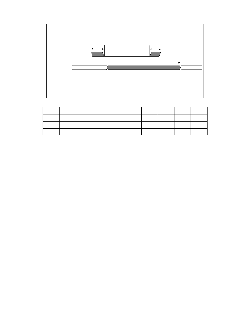
152
t 3
V c c
A l l H o s t
A c c e s s e s
t 2
t 1
FIGURE 3 - POWER-UP TIMING
NAME
DESCRIPTION
MIN
TYP
MAX
UNITS
t1
Vcc Slew from 4.5V to 0V
300
µ
s
t2
Vcc Slew from 0V to 4.5V
100
µ
s
t3
All Host Accesses After Powerup (Note 1)
125
500
µ
s
Note 1: Internal write-protection period after Vcc passes 4.5 volts on power-up
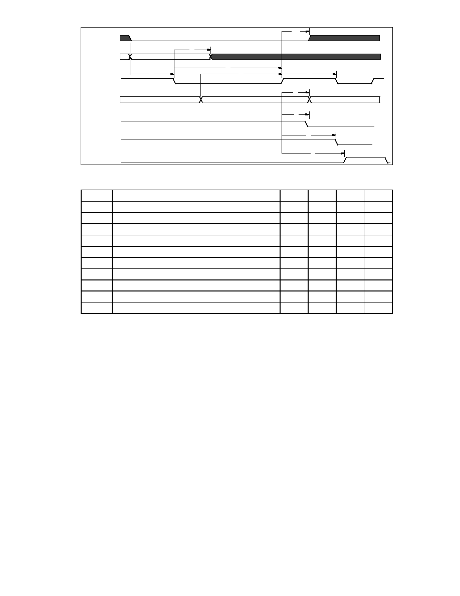
153
FIGURE 4 - ISA WRITE
NAME
DESCRIPTION
MIN
TYP
MAX
UNITS
t1
SA[x], nCS and AEN valid to nIOW asserted
10
ns
t2
nIOW asserted to nIOW deasserted
80
ns
t3
nIOW asserted to SA[x], nCS invalid
10
ns
t4
SD[x] Valid to nIOW deasserted
45
ns
t5
SD[x] Hold from nIOW deasserted
0
ns
t6
nIOW deasserted to nIOW asserted
25
ns
t7
nIOW deasserted to FINTR deasserted (Note 1)
55
ns
t8
nIOW deasserted to PINTER deasserted (Note 2)
260
ns
t9
IBF (internal signal) asserted from nIOW deasserted
40
ns
t10
nIOW deasserted to AEN invalid
10
ns
Note 1: FINTR refers to the IRQ used by the floppy disk.
Note 2: PINTR refers to the IRQ used by the parallel port
t10
t3
t1
t2
t4
t6
t5
t8
t9
DATA VALID
AEN
SA[x], nCS
nIOW
SD[x]
FINTR
PINTR
IBF
t7
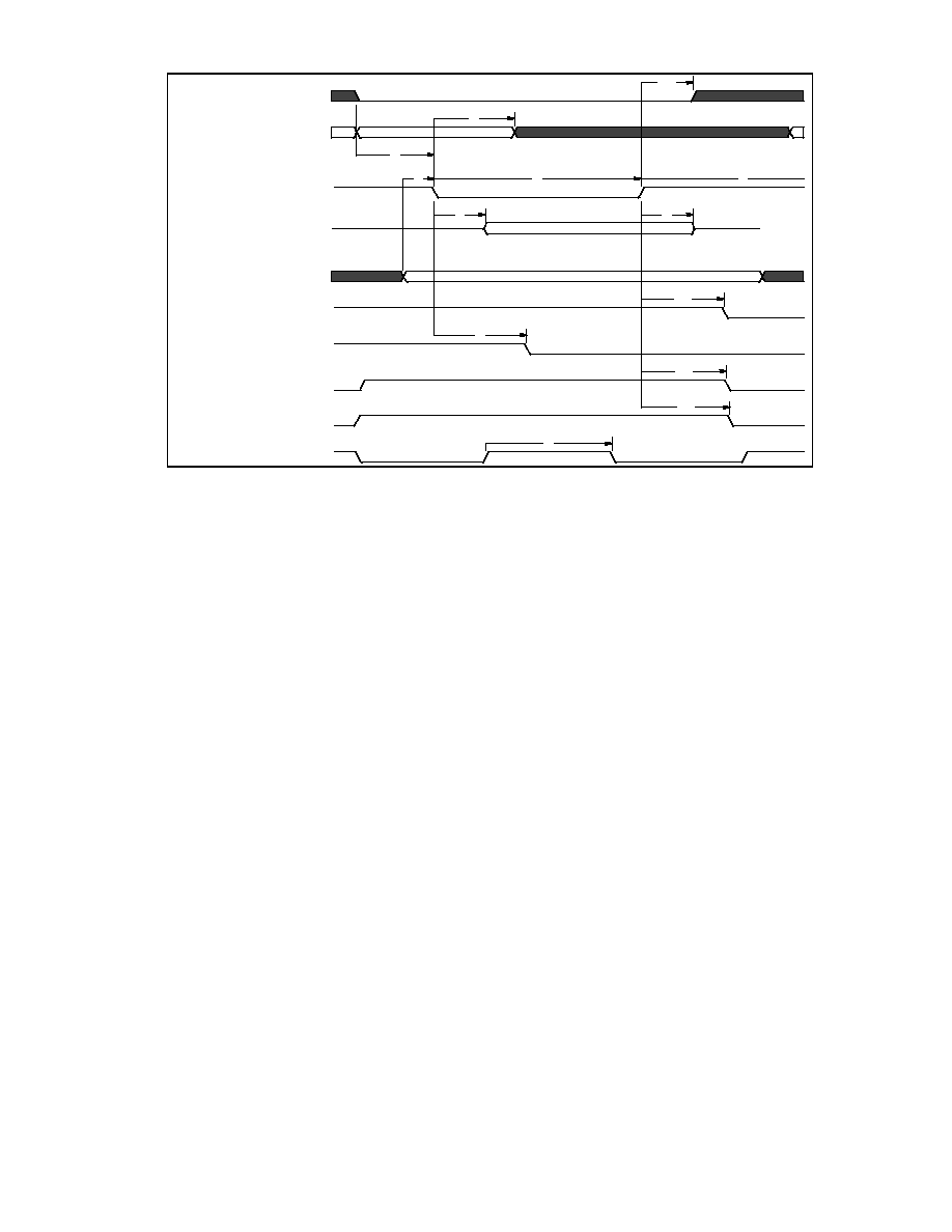
154
FIGURE 5 - ISA READ
SEE TIMING PARAMETERS ON NEXT PAGE
t13
t3
t1
t7
t2
t6
t4
t5
t10
t9
t11
t12
t8
DATA VALID
AEN
SA[x], nCS
nIOR
SD[x]
PD[x], nERROR,
PE, SLCT, ACK, BUSY
FINTER
PINTER
PCOBF
AUXOBF1
nIOR/nIOW

155
ISA READ TIMING
NAME
DESCRIPTION
MIN
TYP
MAX
UNITS
t1
SA[x], nCS and AEN valid to nIOR asserted
10
ns
t2
nIOR asserted to nIOR deasserted
50
ns
t3
nIOR asserted to SA[x], nCS invalid
10
ns
t4
nIOR asserted to Data Valid
50
ns
t5
Data Hold/float from nIOR deasserted
10
25
ns
t6
nIOR deasserted
25
ns
t8
nIOR asserted after nIOW deasserted
80
ns
t8
nIOR/nIOR, nIOW/nIOW transfers from/to ECP FIFO
150
ns
t7
Parallel Port setup to nIOR asserted
20
ns
t9
nIOR asserted to PINTER deasserted
55
ns
t10
nIOR deasserted to FINTER deasserted
260
ns
t11
nIOR deasserted to PCOBF deasserted (Notes 3,5)
80
ns
t12
nIOR deasserted to AUXOBF1 deasserted (Notes 4,5)
80
ns
t13
nIOW deasserted to AEN invalid
10
ns
Note 1: FINTR refers to the IRQ used by the floppy disk.
Note 2: PINTR refers to the IRQ used by the parallel port.
Note 3: PCOBF is used for the Keyboard IRQ.
Note 4: AUXOBF1 is used for the Mouse IRQ.
Note 5: Applies only if deassertion is performed in hardware.
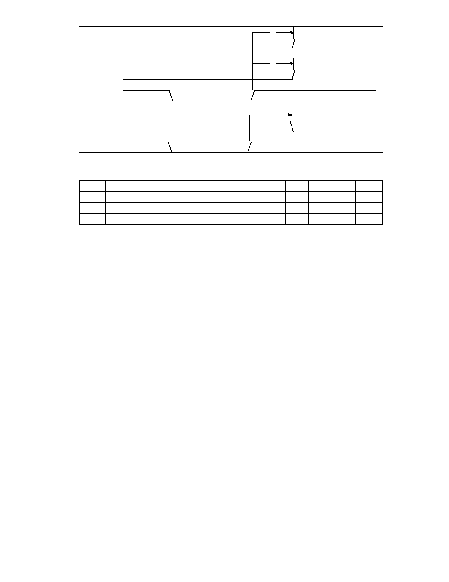
156
FIGURE 6 - INTERNAL 8042 CPU TIMING
NAME
DESCRIPTION
MIN
TYP
MAX
UNITS
t1
nWRT deasserted to AUXOBF1 asserted (Notes 1,2)
40
ns
t2
nWRT deasserted to PCOBF asserted (Notes 1,3)
40
ns
t3
nRD deasserted to IBF deasserted (Note 1)
40
ns
Note 1: IBF, nWRT and nRD are internal signals.
Note 2: PCOBF is used for the Keyboard IRQ.
Note 3: AUXOBF1 is used for the Mouse IRQ.
t2
t1
t3
PCOBF
AUXOBF1
nWRT
IBF
nRD
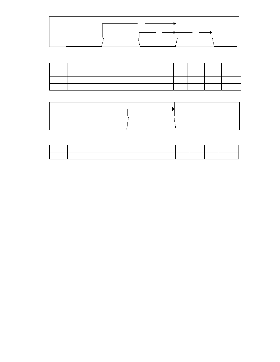
157
FIGURE 7A - INPUT CLOCK TIMING
NAME
DESCRIPTION
MIN
TYP
MAX
UNITS
t1
Clock Cycle Time for 14.318 MHZ
70
ns
t2
Clock High Time/Low Time for 14.318 MHz
35
ns
Clock Rise Time/Fall Time (not shown)
5
ns
FIGURE 7B - RESET TIMING
NAME
DESCRIPTION
MIN
TYP
MAX
UNITS
t4
RESET width (Note 1)
1.5
µ
s
Note 1: The RESET width is dependent upon the processor clock. The RESET must be active while
the clock is running and stable.
t1
t2
t2
CLOCKI
t4
RESET_DRV

158
FIGURE 8A - DMA TIMING (SINGLE TRANSFER MODE)
NAME
DESCRIPTION
MIN
TYP
MAX
UNITS
t1
nDACK Delay Time from FDRQ High
0
ns
t2
DRQ Reset Delay from nIOR or nIOW
100
ns
t3
FDRQ Reset Delay from nDACK Low
100
ns
t4
nDACK Width
150
ns
t5
nIOR Delay from FDRQ High
0
ns
t6
nIOW Delay from FDRQ High
0
ns
t7
Data Access Time from nIOR Low
100
ns
t8
Data Set Up Time to nIOW High
40
ns
t9
Data to Float Delay from nIOR High
10
60
ns
t10
Data Hold Time from nIOW High
10
ns
t11
nDACK Set Up to nIOW/nIOR Low
5
ns
t12
nDACK Hold after nIOW/nIOR High
10
ns
t13
TC Pulse Width
60
ns
t14
AEN Set Up to nIOR/nIOW
40
ns
t15
AEN Hold from nDACK
10
ns
t16
TC Active to PDRQ Inactive
100
ns
t15
t2
t3
t12
t16
t1
t4
t5
t6
t11
t14
t8
t7
t9
t10
t13
AEN
FDRQ,
PDRQ
nDACK
nIOR
or
nIOW
DATA
(DO-D7)
TC
DATA VALID

159
NAME
DESCRIPTION
MIN
TYP
MAX
UNITS
t1
nDACK Delay Time from FDRQ High
0
ns
t2
DRQ Reset Delay from nIOR or nIOW
100
ns
t3
FDRQ Reset Delay from nDACK Low
100
ns
t4
nDACK Width
150
ns
t5
nIOR Delay from FDRQ High
0
ns
t6
nIOW Delay from FDRQ High
0
ns
t7
Data Access Time from nIOR Low
100
ns
t8
Data Set Up Time to nIOW High
40
ns
t9
Data to Float Delay from nIOR High
10
60
ns
t10
Data Hold Time from nIOW High
10
ns
t11
nDACK Set Up to nIOW/nIOR Low
5
ns
t12
nDACK Hold after nIOW/nIOR High
10
ns
t13
TC Pulse Width
60
ns
t14
AEN Set Up to nIOR/nIOW
40
ns
t15
AEN Hold from nDACK
10
ns
t16
TC Active to PDRQ Inactive
100
ns
t15
t2
t3
t12
t16
t1
t4
t5
t6
t11
t14
t8
t7
t9
t10
t13
AEN
FDRQ,
PDRQ
nDACK
nIOR
or
nIOW
DATA
(DO-D7)
TC
DATA VALID
DATA VALID
FIGURE 8B - DMA TIMING (BURST TRANSFER MODE)

160
NAME
DESCRIPTION
MIN
TYP
MAX
UNITS
t1
nDIR Set Up to STEP Low
4
X*
t2
nSTEP Active Time Low
24
X*
t3
nDIR Hold Time after nSTEP
96
X*
t4
nSTEP Cycle Time
132
X*
t5
nDS0-1 Hold Time from nSTEP Low
20
X*
t6
nINDEX Pulse Width
2
X*
t7
nRDATA Active Time Low
40
ns
t8
nWDATA Write Data Width Low
.5
Y*
t9
nDS0-1, MTRO-1 from End of nIOW
25
ns
*X specifies one MCLK period and Y specifies one WCLK period.
MCLK = 16 x Data Rate (at 500 kb/s MCLK = 8 MHz)
WCLK = 2 x Data Rate (at 500 kb/s WCLK = 1 Mhz)
t3
t1
t2
t4
t5
t6
t7
t8
t9
t9
nDIR
nSTEP
nDS0-3
nINDEX
nRDATA
nWDATA
nIOW
nDS0-1,
MTR0-1
FIGURE 9 - DISK DRIVE TIMING (AT MODE ONLY)

161
NAME
DESCRIPTION
MIN
TYP
MAX
UNITS
t1
nRTSx, nDTRx Delay from nIOW
200
ns
t2
IRQx Active Delay from nCTSx, nDSRx, nDCDx
100
ns
t3
IRQx Inactive Delay from nIOR (Leading Edge)
120
ns
t4
IRQx Inactive Delay from nIOW (Trailing Edge)
125
ns
t5
IRQx Inactive Delay from nIOW
10
100
ns
t6
IRQx Active Delay from nRIx
100
ns
t1
t5
t2
t4
t6
t3
nIOW
nRTSx,
nDTRx
IRQx
nCTSx,
nDSRx,
nDCDx
IRQx
nIOW
IRQx
nIOR
nRIx
FIGURE 10 - SERIAL PORT TIMING

162
FIGURE 11 - PARALLEL PORT TIMING
NAME
DESCRIPTION
MIN
TYP
MAX
UNITS
t1
PD0-7, nINIT, nSTROBE, nAUTOFD Delay from
nIOW
100
ns
t2
PINTR Delay from nACK, nFAULT
60
ns
t3
PINTR Active Low in ECP and EPP Modes
200
300
ns
t4
PINTR Delay from nACK
105
ns
t5
nERROR Active to PINTR Active
105
ns
t6
PD0 - PD7 Delay from IOW Active
100
ns
Note:
PINTR refers to the IRQ used by the parallel port.
t1
t4
t3
t2
t2
t5
t3
nIOW
nINIT, nSTROBE.
nAUTOFD, SLCTIN
nACK
PINTR
(ECP or EPP Enabled)
nFAULT (ECP)
nERROR
(ECP)
PINTR
PD0- PD7
t6
nPINTR
(SPP)
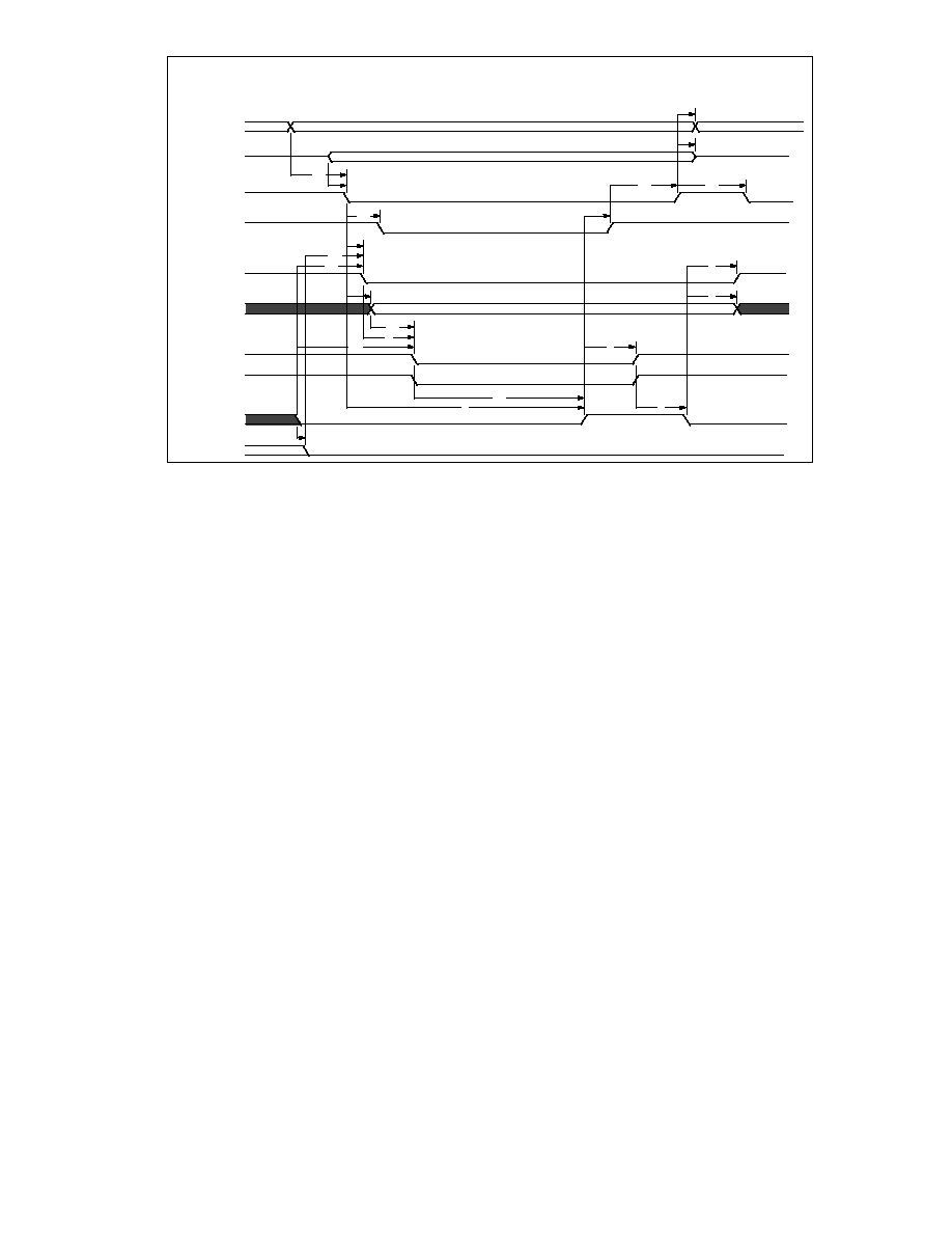
163
FIGURE 12A - EPP 1.9 DATA OR ADDRESS WRITE CYCLE
SEE TIMING PARAMETERS ON NEXT PAGE
t18
t9
t8
t17
t12
t19
t10
t11
t13
t20
t22
t2
t1
t5
t3
t14
t16
t4
t6
t15
t7
t21
A0-A10
SD<7:0>
nIOW
IOCHRDY
nWRITE
PD<7:0>
nDATAST
nADDRSTB
nWAIT
PDIR

164
FIGURE 12B - EPP 1.9 DATA OR ADDRESS WRITE CYCLE TIMING
NAME
DESCRIPTION
MIN
TYP
MAX
UNITS
t1
nIOW Asserted to PDATA Valid
0
50
ns
t2
nWAIT Asserted to nWRITE Change (Note 1)
60
185
ns
t3
nWRITE to Command Asserted
5
35
ns
t4
nWAIT Deasserted to Command Deasserted
(Note 1)
60
190
ns
t5
nWAIT Asserted to PDATA Invalid (Note 1)
0
ns
t6
Time Out
10
12
µ
s
t7
Command Deasserted to nWAIT Asserted
0
ns
t8
SDATA Valid to nIOW Asserted
10
ns
t9
nIOW Deasserted to DATA Invalid
0
ns
t10
nIOW Asserted to IOCHRDY Asserted
0
24
ns
t11
nWAIT Deasserted to IOCHRDY Deasserted
(Note 1)
60
160
ns
t12
IOCHRDY Deasserted to nIOW Deasserted
10
ns
t13
nIOW Asserted to nWRITE Asserted
0
70
ns
t14
nWAIT Asserted to Command Asserted (Note 1)
60
210
ns
t15
Command Asserted to nWAIT Deasserted
0
10
µ
s
t16
PDATA Valid to Command Asserted
10
ns
t17
Ax Valid to nIOW Asserted
40
ns
t18
nIOW Asserted to Ax Invalid
10
ns
t19
nIOW Deasserted to nIOW or nIOR Asserted
40
ns
t20
nWAIT Asserted to nWRITE Asserted (Note 1)
60
185
ns
t21
nWAIT Asserted to PDIR Low
0
ns
t22
PDIR Low to nWRITE Asserted
0
ns
Note 1: nWAIT must be filtered to compensate for ringing on the parallel bus cable. WAIT is
considered to have settled after it does not transition for a minimum of 50 nsec.
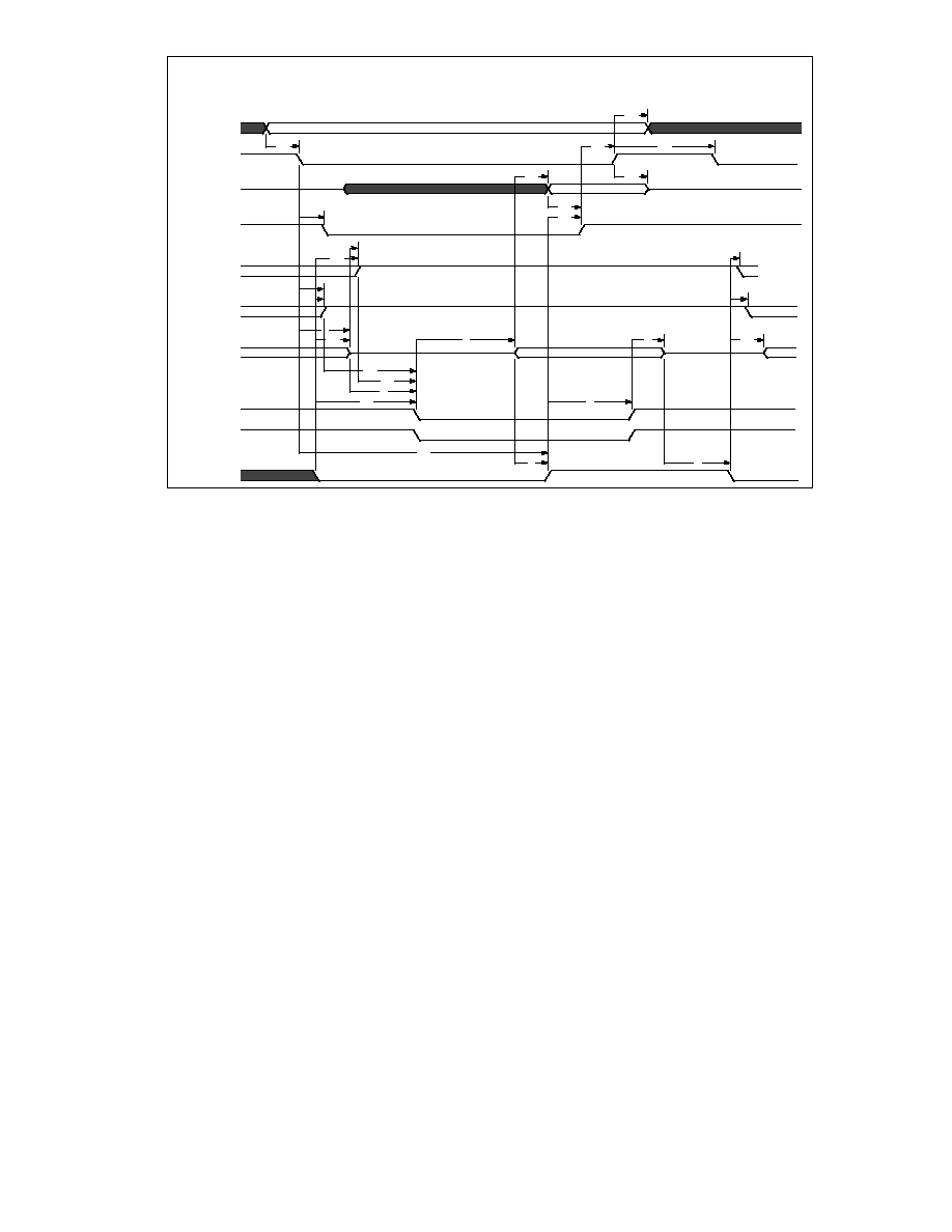
165
FIGURE 13A - EPP 1.9 DATA OR ADDRESS READ CYCLE
SEE TIMING PARAMETERS ON NEXT PAGE
t20
t19
t11
t22
t13
t12
t8
t10
t18
t23
t24
t27
t9
t21
t17
t2
t25
t5
t4
t16
t1
t14
t26
t28
t3
t7
t15
t6
PData bus driven
by peripheral
A0-A10
IOR
SD<7:0>
IOCHRDY
PDIR
nWRITE
PD<7:0>
DATASTB
ADDRSTB
nWAIT

166
FIGURE 13B - EPP 1.9 DATA OR ADDRESS READ CYCLE TIMING PARAMETERS
NAME
DESCRIPTION
MIN
TYP
MAX
UNITS
t1
PDATA Hi-Z to Command Asserted
0
30
ns
t2
nIOR Asserted to PDATA Hi-Z
0
50
ns
t3
nWAIT Deasserted to Command Deasserted
(Note 1)
60
180
ns
t4
Command Deasserted to PDATA Hi-Z
0
ns
t5
Command Asserted to PDATA Valid
0
ns
t6
PDATA Hi-Z to nWAIT Deasserted
0
µ
s
t7
PDATA Valid to nWAIT Deasserted
0
ns
t8
nIOR Asserted to IOCHRDY Asserted
0
24
ns
t9
nWRITE Deasserted to nIOR Asserted (Note 2)
0
ns
t10
nWAIT Deasserted to IOCHRDY Deasserted
(Note 1)
60
160
ns
t11
IOCHRDY Deasserted to nIOR Deasserted
0
ns
t12
nIOR Deasserted to SDATA Hi-Z (Hold Time)
0
40
ns
t13
PDATA Valid to SDATA Valid
0
75
ns
t14
nWAIT Asserted to Command Asserted
0
195
ns
t15
Time Out
10
12
µ
s
t16
nWAIT Deasserted to PDATA Driven (Note 1)
60
190
ns
t17
nWAIT Deasserted to nWRITE Modified (Notes 1,2)
60
190
ns
t18
SDATA Valid to IOCHRDY Deasserted (Note 3)
0
85
ns
t19
Ax Valid to nIOR Asserted
40
ns
t20
nIOR Deasserted to Ax Invalid
10
10
ns
t21
nWAIT Asserted to nWRITE Deasserted
0
185
ns
t22
nIOR Deasserted to nIOW or nIOR Asserted
40
ns
t23
nWAIT Asserted to PDIR Set (Note 1)
60
185
ns
t24
PDATA Hi-Z to PDIR Set
0
ns
t25
nWAIT Asserted to PDATA Hi-Z (Note 1)
60
180
ns
t26
PDIR Set to Command
0
20
ns
t27
nWAIT Deasserted to PDIR Low (Note 1)
60
180
ns
t28
nWRITE Deasserted to Command
1
ns
Note 1:
nWAIT is considered to have settled after it does not transition for a minimum of 50 ns.
Note 2:
When not executing a write cycle, EPP nWRITE is inactive high.
Note 3:
85 is true only if t7 = 0.
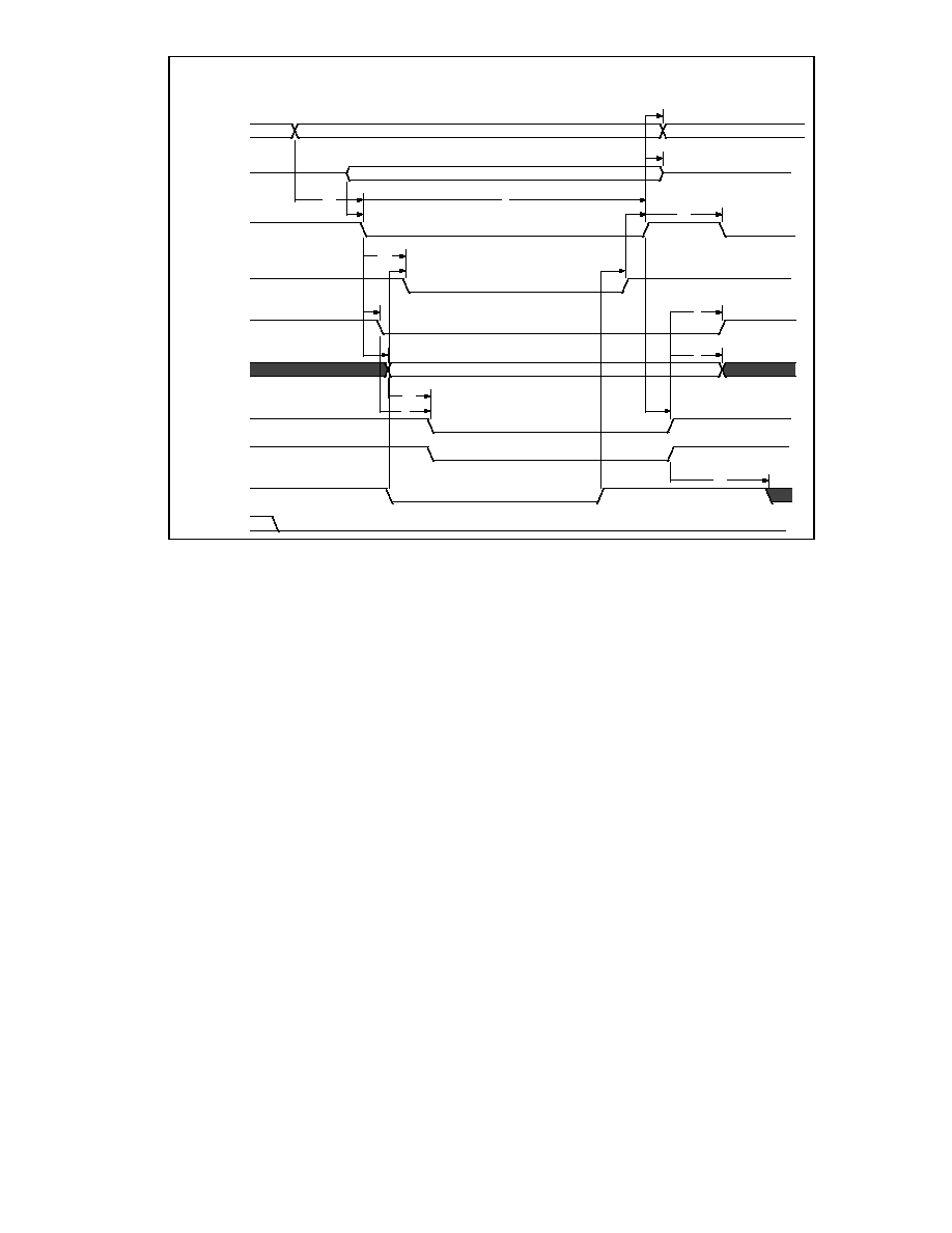
167
FIGURE 14A - EPP 1.7 DATA OR ADDRESS WRITE CYCLE
SEE TIMING PARAMETERS ON NEXT PAGE
t18
t9
t8
t17
t6
t12
t19
t10
t20
t11
t13
t2
t1
t5
t3
t16
t4
t21
A0-A10
SD<7:0>
nIOW
IOCHRDY
nWRITE
PD<7:0>
nDATAST
nADDRSTB
nWAIT
PDIR

168
FIGURE 14B - EPP 1.7 DATA OR ADDRESS WRITE CYCLE PARAMETERS
NAME
DESCRIPTION
MIN
TYP
MAX
UNITS
t1
nIOW Asserted to PDATA Valid
0
50
ns
t2
Command Deasserted to nWRITE Change
0
40
ns
t3
nWRITE to Command
5
35
ns
t4
nIOW Deasserted to Command Deasserted (Note 2)
50
ns
t5
Command Deasserted to PDATA Invalid
50
ns
t6
Time Out
10
12
µ
s
t8
SDATA Valid to nIOW Asserted
10
ns
t9
nIOW Deasserted to DATA Invalid
0
ns
t10
nIOW Asserted to IOCHRDY Asserted
0
24
ns
t11
nWAIT Deasserted to IOCHRDY Deasserted
40
ns
t12
IOCHRDY Deasserted to nIOW Deasserted
10
ns
t13
nIOW Asserted to nWRITE Asserted
0
50
ns
t16
PDATA Valid to Command Asserted
10
35
ns
t17
Ax Valid to nIOW Asserted
40
ns
t18
nIOW Deasserted to Ax Invalid
10
µ
s
t19
nIOW Deasserted to nIOW or nIOR Asserted
100
ns
t20
nWAIT Asserted to IOCHRDY Deasserted
45
ns
t21
Command Deasserted to nWAIT Deasserted
0
ns
Note 1: nWRITE is controlled by clearing the PDIR bit to "0" in the control register before performing
an EPP Write.
Note 2: The number is only valid if nWAIT is active when IOW goes active.

169
FIGURE 15A - EPP 1.7 DATA OR ADDRESS READ CYCLE
SEE TIMING PARAMETERS ON NEXT PAGE
t20
t19
t11
t15
t22
t13
t12
t3
t8
t10
t5
t4
t23
t2
t21
A0-A10
nIOR
SD<7:0>
IOCHRDY
nWRITE
PD<7:0>
nDATASTB
nADDRSTB
nWAIT
PDIR

170
FIGURE 15B - EPP 1.7 DATA OR ADDRESS READ CYCLE PARAMETERS
NAME
DESCRIPTION
MIN
TYP
MAX
UNITS
t2
nIOR Deasserted to Command Deasserted
50
ns
t3
nWAIT Asserted to IOCHRDY Deasserted
0
40
ns
t4
Command Deasserted to PDATA Hi-Z
0
ns
t5
Command Asserted to PDATA Valid
0
ns
t8
nIOR Asserted to IOCHRDY Asserted
24
ns
t10
nWAIT Deasserted to IOCHRDY Deasserted
50
ns
t11
IOCHRDY Deasserted to nIOR Deasserted
0
ns
t12
nIOR Deasserted to SDATA High-Z (Hold Time)
0
40
ns
t13
PDATA Valid to SDATA Valid
40
ns
t15
Time Out
10
12
µ
s
t19
Ax Valid to nIOR Asserted
40
ns
t20
nIOR Deasserted to Ax Invalid
10
ns
t21
Command Deasserted to nWAIT Deasserted
0
ns
t22
nIOR Deasserted to nIOW or nIOR Asserted
40
ns
t23
nIOR Asserted to Command Asserted
55
ns
Note:
WRITE is controlled by setting the PDIR bit to "1" in the control register before performing an
EPP Read.

171
ECP PARALLEL PORT TIMING
Parallel Port FIFO (Mode 101)
The standard parallel port is run at or near the
peak 500KBytes/sec allowed in the forward
direction using DMA. The state machine does
not examine nACK and begins the next transfer
based on Busy. Refer to Figure 17.
ECP Parallel Port Timing
The timing is designed to allow operation at
approximately 2.0 Mbytes/sec over a 15ft cable.
If a shorter cable is used then the bandwidth will
increase.
Forward-Idle
When the host has no data to send it keeps
HostClk (nStrobe) high and the peripheral will
leave PeriphClk (Busy) low.
Forward Data Transfer Phase
The interface transfers data and commands
from the host to the peripheral using an inter-
locked PeriphAck and HostClk. The peripheral
may indicate its desire to send data to the host
by asserting nPeriphRequest.
The Forward Data Transfer Phase may be
entered from the Forward-Idle Phase. While in
the Forward Phase the peripheral may
asynchronously assert the nPeriphRequest
(nFault) to request that the channel be reversed.
When the peripheral is not busy it sets
PeriphAck (Busy) low. The host then sets
HostClk (nStrobe) low when it is prepared to
send data. The data must be stable for the
specified setup time prior to the falling edge of
HostClk. The peripheral then sets PeriphAck
(Busy) high to acknowledge the handshake. The
host then sets HostClk (nStrobe) high. The
peripheral then accepts the data and sets
PeriphAck (Busy) low, completing the transfer.
This sequence is shown in Figure 17.
The timing is designed to provide 3 cable
round-trip times for data setup if Data is driven
simultaneously with HostClk (nStrobe).
Reverse-Idle Phase
The peripheral has no data to send and keeps
PeriphClk high. The host is idle and keeps
HostAck low.
Reverse Data Transfer Phase
The interface transfers data and commands
from the peripheral to the host using an inter-
locked HostAck and PeriphClk.
The Reverse Data Transfer Phase may be en-
tered from the Reverse-Idle Phase. After the
previous byte has beed accepted the host sets
HostAck (nALF) low. The peripheral then sets
PeriphClk (nACK) low when it has data to send.
The data must be stable for the specified setup
time prior to the falling edge of PeriphClk. When
the host is ready to accept a byte it sets
HostAck (nALF) high to acknowledge the
handshake. The peripheral then sets PeriphClk
(nACK) high. After the host has accepted the
data it sets HostAck (nALF) low, completing the
transfer. This sequence is shown in Figure 18.
Output Drivers
To facilitate higher performance data transfer,
the use of balanced CMOS active drivers for
critical signals (Data, HostAck, HostClk,
PeriphAck, PeriphClk) are used ECP Mode.
Because the use of active drivers can present
compatibility problems in Compatible Mode
(the control signals, by tradition, are specified
as open-collector), the drivers are dynamically
changed from open-collector to totem-pole. The

172
timing for the dynamic driver change is
specified in then IEEE 1284 Extended
Capabilities Port Protocol and ISA
Interface Standard, Rev. 1.14, July 14, 1993,
available from Microsoft. The dynamic driver
change must be implemented properly to
prevent glitching the outputs.
FIGURE 16 - PARALLEL PORT FIFO TIMING
NAME
DESCRIPTION
MIN
TYP
MAX
UNITS
t1
DATA Valid to nSTROBE Active
600
ns
t2
nSTROBE Active Pulse Width
600
ns
t3
DATA Hold from nSTROBE Inactive (Note 1)
450
ns
t4
nSTROBE Active to BUSY Active
500
ns
t5
BUSY Inactive to nSTROBE Active
680
ns
t6
BUSY Inactive to PDATA Invalid (Note 1)
80
ns
Note 1: The data is held until BUSY goes inactive or for time t3, whichever is longer. This only
applies if another data transfer is pending. If no other data transfer is pending, the data is
held indefinitely.
t3
t6
t1
t2
t5
t4
PDATA
nSTROBE
BUSY

173
t3
t4
t1
t2
t7
t8
t6
t5
t6
nAUTOFD
PDATA<7:0>
BUSY
nSTROBE
FIGURE 17 - ECP PARALLEL PORT FORWARD TIMING
NAME
DESCRIPTION
MIN
TYP
MAX
UNITS
t1
nAUTOFD Valid to nSTROBE Asserted
0
60
ns
t2
PDATA Valid to nSTROBE Asserted
0
60
ns
t3
BUSY Deasserted to nAUTOFD Changed
(Notes 1,2)
80
180
ns
t4
BUSY Deasserted to PDATA Changed (Notes 1,2)
80
180
ns
t5
nSTROBE Deasserted to Busy Asserted
0
ns
t6
nSTROBE Deasserted to Busy Deasserted
0
ns
t7
BUSY Deasserted to nSTROBE Asserted (Notes 1,2)
80
200
ns
t8
BUSY Asserted to nSTROBE Deasserted (Note 2)
80
180
ns
Note 1: Maximum value only applies if there is data in the FIFO waiting to be written out.
Note 2: BUSY is not considered asserted or deasserted until it is stable for a minimum of 75 to 130
ns.
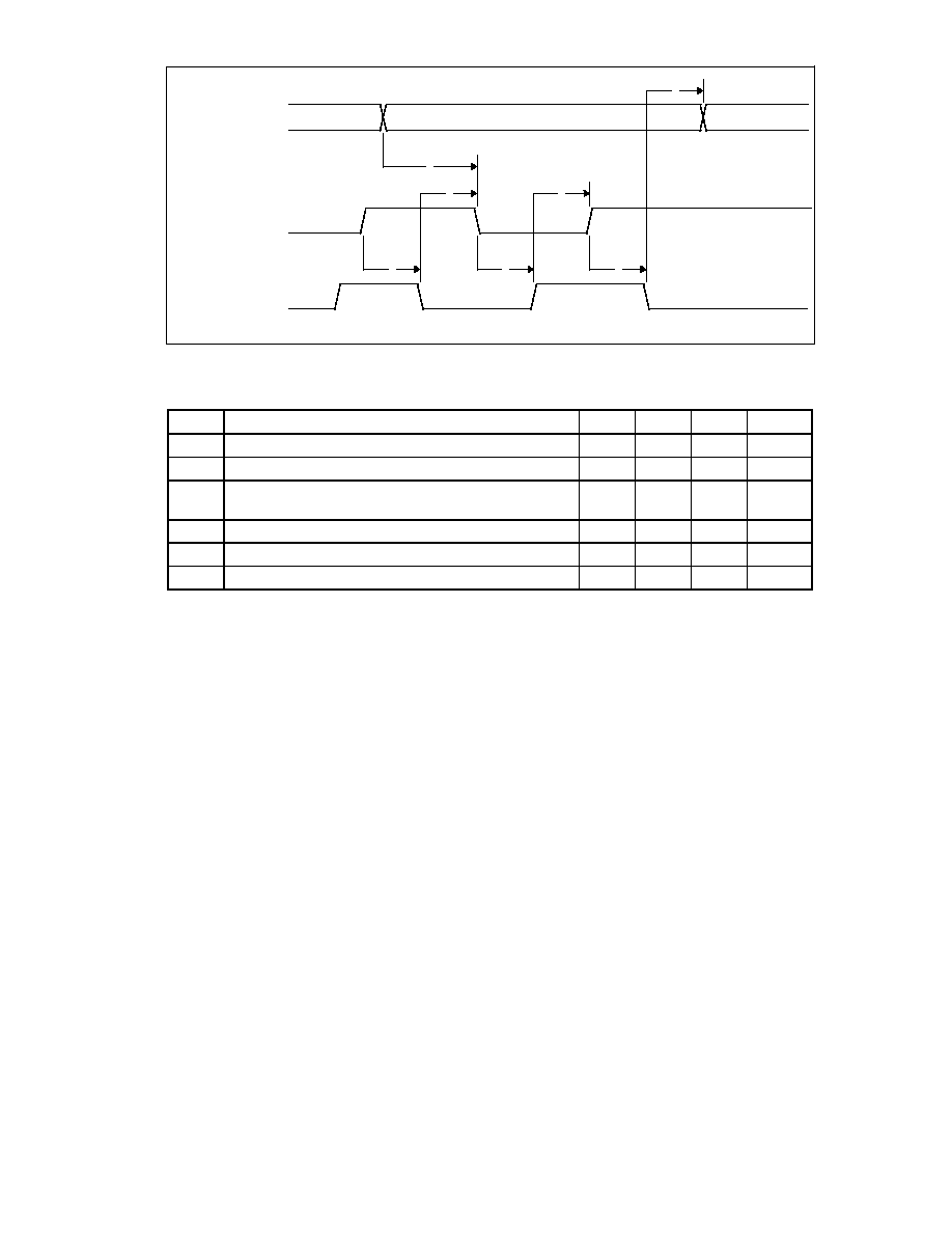
174
t2
t1
t5
t6
t4
t3
t4
PDATA<7:0>
nACK
nAUTOFD
FIGURE 18 - ECP PARALLEL PORT REVERSE TIMING
NAME
DESCRIPTION
MIN
TYP
MAX
UNITS
t1
PDATA Valid to nACK Asserted
0
ns
t2
nAUTOFD Deasserted to PDATA Changed
0
ns
t3
nACK Asserted to nAUTOFD Deasserted
(Notes 1,2)
80
200
ns
t4
nACK Deasserted to nAUTOFD Asserted (Note 2)
80
200
ns
t5
nAUTOFD Asserted to nACK Asserted
0
ns
t6
nAUTOFD Deasserted to nACK Deasserted
0
ns
Note 1: Maximum value only applies if there is room in the FIFO and terminal count has not been
received. ECP can stall by keeping nAUTOFD low.
Note 2: nACK is not considered asserted or deasserted until it is stable for a minimum of 75 to 130
ns.
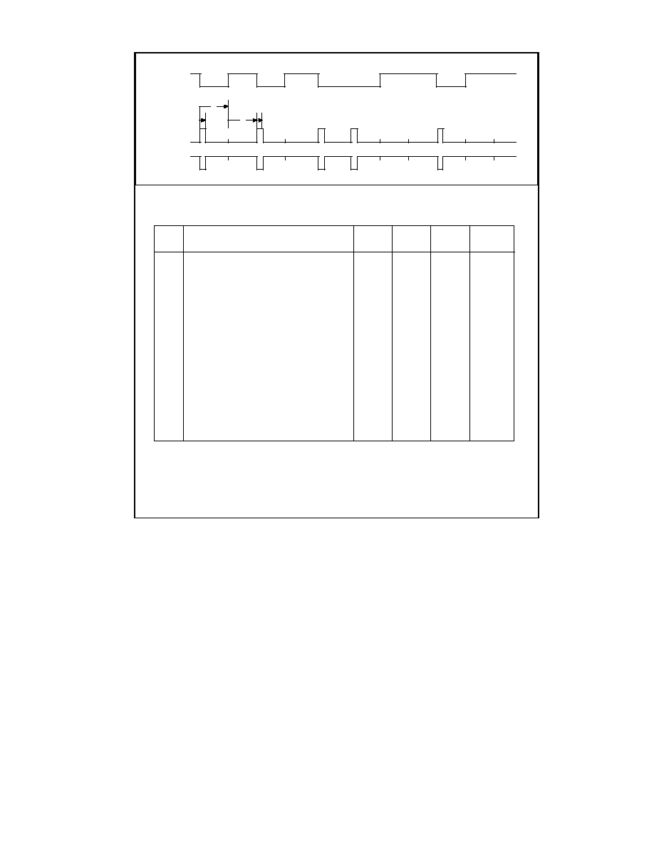
175
t1
t2
t2
t1
0
1
0
1
0
0
1
1
0
1
1
DATA
IRRX
n IRRX
t1
t1
t1
t1
t1
t1
t1
t2
t2
t2
t2
t2
t2
t2
Parameter
min
typ
max
units
1.4
1.4
1.4
1.4
1.4
1.4
1.4
2.71
3.69
5.53
11.07
22.13
44.27
88.55
µs
µs
µs
µs
µs
µs
µs
µs
µs
µs
µs
µs
µs
µs
Pulse Width at 115kbaud
Pulse Width at 57.6kbaud
Pulse Width at 38.4kbaud
Pulse Width at 19.2kbaud
Pulse Width at 9.6kbaud
Pulse Width at 4.8kbaud
Pulse Width at 2.4kbaud
Bit Time at 115kbaud
Bit Time at 57.6kbaud
Bit Time at 38.4kbaud
Bit Time at 19.2kbaud
Bit Time at 9.6kbaud
Bit Time at 4.8kbaud
Bit Time at 2.4kbaud
1.6
3.22
4.8
9.7
19.5
39
78
8.68
17.4
26
52
104
208
416
Notes:
1. Receive Pulse Detection Criteria: A received pulse is considered detected if the
received pulse is a minimum of 1.41µs.
2. IRRX: L5, CRF1 Bit 0: 1 = RCV active low
nIRRX: L5, CRF1 Bit 0: 0 = RCV active high (default)
FIGURE 19 - IrDA RECEIVE TIMING

176
FIGURE 20 - IrDA TRANSMIT TIMING
t1
t1
t1
t1
t1
t1
t1
t2
t2
t2
t2
t2
t2
t2
Parameter
min
typ
max
units
1.41
1.41
1.41
1.41
1.41
1.41
1.41
2.71
3.69
5.53
11.07
22.13
44.27
88.55
µs
µs
µs
µs
µs
µs
µs
µs
µs
µs
µs
µs
µs
µs
Pulse W idth at 115kbaud
Pulse W idth at 57.6kbaud
Pulse W idth at 38.4kbaud
Pulse W idth at 19.2kbaud
Pulse W idth at 9.6kbaud
Pulse W idth at 4.8kbaud
Pulse W idth at 2.4kbaud
Bit Time at 115kbaud
Bit Time at 57.6kbaud
Bit Time at 38.4kbaud
Bit Time at 19.2kbaud
Bit Time at 9.6kbaud
Bit Time at 4.8kbaud
Bit Time at 2.4kbaud
1.6
3.22
4.8
9.7
19.5
39
78
8.68
17.4
26
52
104
208
416
t1
t2
t2
t1
0
1
0
1
0
0
1
1
0
1
1
DATA
IRTX
n IRTX
Notes:
1. IrDA @ 115k is HPSIR compatible. IrDA @ 2400 will allow compatibility with HP95LX
and 48SX.
2. IRTX: L5, CRF1 Bit 1: 1 = XMIT active low (default)
nIRTX: L5, CRF1 Bit 1: 0 = XMIT active high
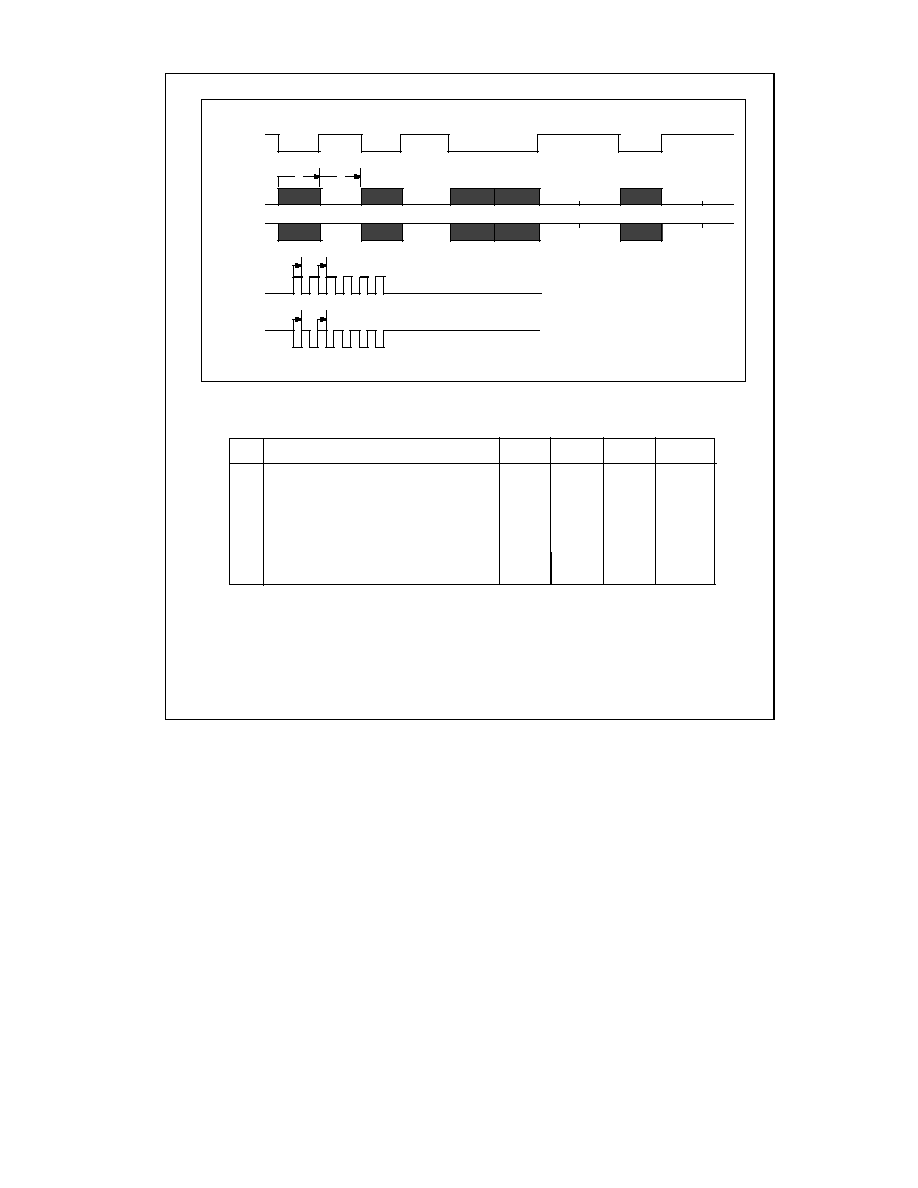
177
FIGURE 21 - AMPLITUDE SHIFT KEYED IR RECEIVE TIMING
t1
t2
t3
t4
t5
t6
Parameter
min
typ
max
units
0.8
0.8
0.8
0.8
1.2
1.2
1.2
1.2
µs
µs
µs
µs
µs
µs
Modulated Output Bit Time
Off Bit Time
Modulated Output "On"
Modulated Output "Off"
Modulated Output "On"
Modulated Output "Off"
1
1
1
1
Notes:
1. IRRX: L5, CRF1 Bit 0: 1 = RCV active low
nIRRX: L5, CRF1 Bit 0: 0 = RCV active high (default)
MIRRX, nMIRRX are the modulated outputs
t1
t2
t3
t4
t5
t6
0
1
0
1
0
0
1
1
0
1
1
D A T A
IRRX
n IRRX
MIRRX
nMIRRX

178
FIGURE 22 - AMPLITUDE SHIFT KEYED IR TRANSMIT TIMING
t1
t2
t3
t4
t5
t6
Parameter
min
typ
max
units
0.8
0.8
0.8
0.8
1.2
1.2
1.2
1.2
µs
µs
µs
µs
µs
µs
Modulated Output Bit Time
Off Bit Time
Modulated Output "On"
Modulated Output "Off"
Modulated Output "On"
Modulated Output "Off"
1
1
1
1
Notes:
1. IRTX: L5, CRF1 Bit 1: 1 = XMIT active low (default)
nIRTX: L5, CRF1 Bit 1: 0 = XMIT active high
MIRTX, nMIRTX are the modulated outputs
t1
t2
t3
t4
t5
t6
0
1
0
1
0
0
1
1
0
1
1
DATA
IRTX
n IRTX
MIRTX
nMIRTX

179
FIGURE 23 - 100 PIN QFP PACKAGE OUTLINE
0 . 1 0
- C -
H
A
A 1
A 2
T D / T E
0
L 1
L
E 1
E
D 1
D
e
W
N o t e s :
1 ) C o p l a n a r i t y i s 0 . 1 0 0 m m ( . 0 0 4 " ) m a x i m u m .
2 ) T o l e r a n c e o n t h e p o s i t i o n o f t h e l e a d s i s
0 . 2 0 0 m m ( . 0 0 8 " ) m a x i m u m .
3 ) P a c k a g e b o d y d i m e n s i o n s D 1 a n d E 1 d o n o t
i n c l u d e t h e m o l d p r o t r u s i o n . M a x i m u m m o l d
p r o t r u s i o n i s 0 . 2 5 m m ( . 0 1 0 " ) .
4 ) D i m e n s i o n s T D a n d T E a r e i m p o r t a n t f o r t e s t i n g
b y r o b o t i c h a n d l e r . O n l y a b o v e c o m b i n a t i o n s o f ( 1 )
o r ( 2 ) a r e a c c e p t a b l e .
5 ) C o n t r o l l i n g d i m e n s i o n : m i l l i m e t e r . D i m e n s i o n s
i n i n c h e s f o r r e f e r e n c e o n l y a n d n o t n e c e s s a r i l y
a c c u r a t e .
D I M
A
A 1
A 2
D
D 1
E
E 1
H
L
L 1
e
0
W
T D ( 1 )
T E ( 1 )
T D ( 2 )
T E ( 2 )
M I N
2 . 8 0
0 . 1
2 . 5 7
2 3 . 4
1 9 . 9
1 7 . 4
1 3 . 9
0 . 1
0 . 6 5
1 . 8
M A X
3 . 1 5
0 . 4 5
2 . 8 7
2 4 . 1 5
2 0 . 1
1 8 . 1 5
1 4 . 1
0 . 2
0 . 9 5
2 . 6
M I N
. 1 1 0
. 0 0 4
. 1 0 1
. 9 2 1
. 7 8 3
. 6 8 5
. 5 4 7
. 0 0 4
. 0 2 6
. 0 7 1
M A X
. 1 2 4
. 0 1 8
. 1 1 3
. 9 5 1
. 7 9 1
. 7 1 5
. 5 5 5
. 0 0 8
. 0 3 7
. 1 0 2
0 ∞
.2
2 1 . 8
1 5 . 8
2 2 . 2 1
1 6 . 2 7
1 2 ∞
.4
2 2 . 2
1 6 . 2
2 2 . 7 6
1 6 . 8 2
0 . 6 5 B S C
0 ∞
. 0 0 8
. 8 5 8
. 6 2 2
. 8 7 4
. 6 4 1
1 2 ∞
. 0 1 6
. 8 7 4
. 6 3 8
. 8 9 6
. 6 6 2
. 0 2 5 6 B S C

180
FDC37M60x ERRATA SHEET
PAGE
SECTION /FIGURE/ENTRY
CORRECTION
DATE
REVISED
7
Description of Pin Functions
Pin #2/IR Mode Reference Taken out
6/6/97
9
Description of Multifunction
PIns
Row #1 Removed
6/6/97
80
Infrared Interface
See Italicized Text
6/6/97
81
Parallel Port
The parallel port FDC is not
supported
6/6/97
108
Serial IRQ
SMI Reference taken out
6/6/97
111
Table 47/Note
See Italicized Text
6/6/97
120
8042 P12 and P16
Functions/2nd Paragraph
Reference to nSMI Removed
6/6/97
124
Table 52
See Italicized Text
6/6/97
142
Table 64
See Italicized Text
6/6/97

181

©
1997 STANDARD MICROSYSTEMS
CORP.
Circuit diagrams utilizing SMSC products are included as a means of illustrating
typical applications; consequently complete information sufficient for construction
purposes is not necessarily given. The information has been carefully checked
and is believed to be entirely reliable. However, no responsibility is assumed for
inaccuracies. Furthermore, such information does not convey to the purchaser of
the semiconductor devices described any licenses under the patent rights of
SMSC or others. SMSC reserves the right to make changes at any time in order to
improve design and supply the best product possible. SMSC products are not
designed, intended, authorized or warranted for use in any life support or other
application where product failure could cause or contribute to personal injury or
severe property damage. Any and all such uses without prior written approval of
an Officer of SMSC and further testing and/or modification will be fully at the risk of
the customer.
FDC37M60x Rev. 6/6/97