
FDC37M81x
PC98/99 Compliant Enhanced Super I/O
Controller with Keyboard/Mouse Wake-Up
FEATURES
!"
5 Volt Operation
!"
PC98, PC99 Compliant
!"
ISA Plug-and-Play Compatible Register Set
!"
Intelligent Auto Power Management
-
Shadowed Write-Only Registers
-
Programmable Wake-up Event
Interface
!"
System Management Interrupt, Watchdog
Timer
!"
2.88MB Super I/O Floppy Disk Controller
-
Licensed CMOS 765B Floppy Disk
Controller
-
Software and Register Compatible
with SMSC's Proprietary 82077AA
Compatible
Core
-
Supports One Floppy Drive
-
Configurable Open Drain/Push-Pull
Output
Drivers
-
Supports Vertical Recording Format
-
16-Byte Data FIFO
-
100% IBM Compatibility
-
Detects All Overrun and Underrun
Conditions
-
Sophisticated Power Control Circuitry
(PCC) Including Multiple Powerdown
Modes for Reduced Power
Consumption
-
DMA Enable Logic
-
Data Rate and Drive Control Registers
-
480 Address, Up to 15 IRQ and
Three
DMA
Options
!"
Floppy Disk Available on Parallel Port Pins
!"
Enhanced Digital Data Separator
-
2 Mbps, 1 Mbps, 500 Kbps, 300
Kbps, 250 Kbps Data Rates
-
Programmable Precompensation
Modes
!"
Keyboard Controller
-
8042 Software Compatible
-
8 Bit Microcomputer
-
2k Bytes of Program ROM
-
256 Bytes of Data RAM
-
Four Open Drain Outputs Dedicated
for
Keyboard/Mouse
Interface
-
Asynchronous Access to Two Data
Registers and One Status Register
-
Supports Interrupt and Polling Access
-
8 Bit Counter Timer
-
Port 92 Support
-
Fast Gate A20 and KRESET Outputs
-
8042 P12, P16 and P17 Outputs
!"
Serial Ports
-
Two Full Function Serial Ports
-
High Speed NS16C550A Compatible
UARTs with Send/Receive 16-Byte
FIFOs
-
Supports 230k and 460k Baud
Programmable Baud Rate Generator
Modem
Control
Circuitry
-
480 Address and 15 IRQ Options
-
IrDA 1.0, HP-SIR, ASK IR Support

2
!"
Multi-Mode Parallel Port with ChiProtect
-
Standard Mode IBM PC/XT PC/AT,
and PS/2 Compatible Bidirectional
Parallel Port
-
Enhanced Parallel Port (EPP)
Compatible - EPP 1.7 and EPP 1.9
(IEEE
1284
Compliant)
-
IEEE 1284 Compliant Enhanced
Capabilities
Port
(ECP)
-
ChiProtect Circuitry for Protection
Against Damage Due to Printer Power-
On
-
480 Address, Up to 15 IRQ and
Three DMA Options
!"
ISA Host Interface
-
16 Bit Address Qualification
-
8 Bit Data Bus
-
IOCHRDY for ECP and IrCC
-
Three 8 Bit DMA Channels
-
Serial IRQ Interface Compatible with
Serialized IRQ Support for PCI Systems
- PME
Interface
!"
100 Pin QFP Package
GENERAL DESCRIPTION
The FDC37M81x* with IrDA v1.0 support
incorporates a keyboard interface, SMSC's true
CMOS 765B floppy disk controller, advanced
digital data separator, two 16C550A compatible
UARTs, one Multi-Mode parallel port which
includes ChiProtect circuitry plus EPP and ECP,
on-chip 12 mA AT bus drivers, one floppy direct
drive support, and Intelligent Power
Management including PME support. The true
CMOS 765B core provides 100% compatibility
with IBM PC/XT and PC/AT architectures in
addition to providing data overflow and
underflow protection. The SMSC advanced
digital data separator incorporates SMSC's
patented data separator technology, allowing for
ease of testing and use. Both on-chip UARTs
are compatible with the NS16C550A. The
parallel port is compatible with IBM PC/AT
architecture, as well as IEEE 1284 EPP and
ECP. The FDC37M81x incorporates
sophisticated power control circuitry (PCC)
which includes support for keyboard, mouse,
and modem ring wake-up events. The PCC
supports multiple low power-down modes.
The FDC37M81x supports the ISA Plug-and-
Play Standard (Version 1.0a) and provides the
recommended functionality to support Windows
'95/'98. The I/O Address, DMA Channel and
hardware IRQ of each logical device in the
FDC37M81x may be reprogrammed through the
internal configuration registers. There are 480
I/O address location options, a Serialized IRQ
interface, and three DMA channels.
The FDC37M81x does not require any external
filter components and is therefore easy to use
and offers lower system costs and reduced
board area. The FDC37M81x is software and
register compatible with SMSC's proprietary
82077AA core.
*The "x" in the part number is a designator that changes depending upon the particular BIOS used inside
the specific chip. "2" denotes AMI Keyboard BIOS and "7" denotes Phoenix 42i Keyboard BIOS.

3
TABLE OF CONTENTS
FEATURES ....................................................................................................................................... 1
GENERAL DESCRIPTION ................................................................................................................ 2
PIN CONFIGURATION...................................................................................................................... 5
DESCRIPTION OF PIN FUNCTIONS ................................................................................................ 6
Buffer Type Descriptions ............................................................................................................... 9
Description of Multifunction Pins ................................................................................................. 10
REFERENCE DOCUMENTS ........................................................................................................... 10
POWER FUNCTIONALITY .............................................................................................................. 12
VCC Power ................................................................................................................................. 12
VTR Support ............................................................................................................................... 12
Internal PWRGOOD.................................................................................................................... 12
Trickle Power Functionality.......................................................................................................... 13
Maximum Current Values ............................................................................................................ 13
Power Management Events (PME/SCI) ....................................................................................... 13
FUNCTIONAL DESCRIPTION......................................................................................................... 14
Super I/O Registers..................................................................................................................... 14
Host Processor Interface ............................................................................................................. 14
FLOPPY DISK CONTROLLER........................................................................................................ 15
FDC Internal Registers ................................................................................................................ 15
Command Set/Descriptions......................................................................................................... 38
Instruction Set............................................................................................................................. 41
SERIAL PORT (UART).................................................................................................................... 68
INFRARED INTERFACE ................................................................................................................. 82
PARALLEL PORT........................................................................................................................... 83
IBM XT/AT Compatible, Bi-Directional And Epp Modes................................................................ 85
Extended Capabilities Parallel Port.............................................................................................. 91
PARALLEL PORT FLOPPY DISK CONTROLLER .........................................................................104
POWER MANAGEMENT ...............................................................................................................106
SERIAL IRQ...................................................................................................................................112
GP INDEX REGISTERS .................................................................................................................116
WATCH DOG TIMER .....................................................................................................................118
8042 KEYBOARD CONTROLLER DESCRIPTION .........................................................................119
Latches On Keyboard And Mouse IRQs .....................................................................................128
Keyboard and Mouse PME Generation .......................................................................................129

4
SYSTEM MANAGEMENT INTERRUPT (SMI) .................................................................................. 131
PME SUPPORT ................................................................................................................................. 132
CONFIGURATION ............................................................................................................................. 133
OPERATIONAL DESCRIPTION........................................................................................................ 164
Maximum Guaranteed Ratings...................................................................................................... 164
DC Electrical Characteristics......................................................................................................... 164
TIMING DIAGRAMS .......................................................................................................................... 169
5
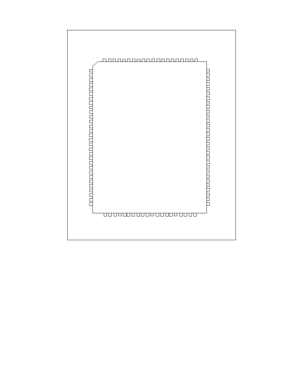
PIN CONFIGURATION
FDC37M81x
100 PIN QFP
1
2
3
4
5
6
7
8
9
10
11
12
13
14
15
16
17
18
19
20
21
22
23
24
25
26
27
28
29
30
DRVDEN0
DRVDEN1
nMTR0
nIO_PME
nDS0
P17
VSS
nDIR
nSTEP
nWDATA
nWGATE
nHDSEL
nINDEX
nTRK0
nWPRT
nRDATA
nDSKCHG
VTR
CLOCKI
nCS/SA11
SA10
SA9
SA8
SA7
SA6
SA5
SA4
SA3
SA2
SA1
80
79
78
77
76
75
74
73
72
71
70
69
68
67
66
65
64
63
62
61
60
59
58
57
56
55
54
53
52
51
PE
SLCT
nERROR
nACK
VSS
PD0
PD1
PD2
PD3
PD4
PD5
PD6
PD7
nINIT
nSLCTIN
VCC
KBRST
A20M
IRTX2
IRRX2
VSS
KDAT
KCLK
MDAT
MCLK
IOCHRDY
TC
VCC
DRQ3/P12
nDACK3/P16
B
U
S
Y
n
A
L
F
n
S
T
R
O
B
E
R
X
D
1
T
X
D
1
n
D
S
R
1
n
R
T
S
1
/
S
Y
S
O
P
T
n
C
T
S
1
n
D
T
R
1
n
R
I
1
n
D
C
D
1
n
R
I
2
/
P
1
6
V
C
C
n
D
C
D
2
/
P
1
2
R
X
D
2
/
I
R
R
X
n
D
S
R
2
/
S
A
1
5
T
X
D
2
/
I
R
T
X
n
C
T
S
2
/
S
A
1
3
n
R
T
S
2
/
S
A
1
2
n
D
T
R
2
/
S
A
1
4
1
0
0
9
9
9
8
9
7
9
6
9
5
9
4
9
3
9
2
9
1
9
0
8
9
8
8
8
7
8
6
8
5
8
4
8
3
8
2
8
1
D
R
Q
1
n
D
A
C
K
1
R
E
S
E
T
_
D
R
V
S
D
0
S
D
1
S
D
2
S
D
3
V
S
S
S
D
4
S
D
5
S
D
6
S
D
7
n
I
O
W
n
I
O
R
A
E
N
S
E
R
_
I
R
Q
P
C
I
_
C
L
K
S
A
0
n
D
A
C
K
2
D
R
Q
2
3
1
3
2
3
3
3
4
3
5
3
6
3
7
3
8
3
9
4
0
4
1
4
2
4
3
4
4
4
5
4
6
4
7
4
8
4
9
5
0