IrCC
Infrared Communications Controller
FEATURES
∑
Multi-Protocol Serial Communications
Controller
∑
Full IrDA v1.1 Implementation: 2.4Kbps,
115.2Kbps, .576Mbps, 1.152Mbps and
4Mbps
∑
Consumer Infrared (TV Remote Control)
Interface
∑
SHARP Amplitude Shift Keyed Infrared
(ASK IR) Interface
∑
Direct Rx/Tx Infrared Diode Control (Raw)
and General Purpose Data Pins
∑
Programmable High-Speed Synchronous
Communications Engine (SCE) with a 128-
Byte FIFO and Programmable Threshold
∑
High-Speed NS16C550A-Compatible
Universal Asynchronous Receiver/
Transmitter Interface (ACE UART2) with 16-
Byte Send and Receive FIFOs
∑
ISA Single-Byte and Burst-Mode DMA and
Interrupt-Driven Programmed I/O with Zero
Wait State and String Move Timing
∑
16-bit CRC-CCITT and 32-bit IEEE 802
CRC32 Hardware CRC Generators
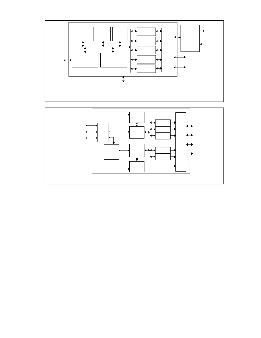
GENERAL DESCRIPTION
This document describes the Infrared
Communications Controller (IrCC) function which
is common to a number of SMSC products
including the FDC37C669FR, FDC37C93xFR,
and FDC37C957FR devices. The IrCC consists
of two main architectural blocks: the ACE
16550A UART and a Synchronous
Communications Engine (SCE) (Figure 2). Each
block is supported by its own unique register set.
The IrCC UART-driven IrDA SIR and SHARP
ASK modes are backward-compatible with early
SMSC Super I/O and Ultra I/O infrared
implementations. The IrCC SCE supports IrDA
v1.1 .576Mbps, 1.152Mbps, 4Mbps, and
Consumer IR modes. All of the SCE modes use
DMA. The IrCC offers flexible signal routing and
programmable output control through the Raw
mode interface, General Purpose Data pins and
Output Multiplexer. Chip-level address decoding
is required to access the IrCC register sets.

2
TABLE OF CONTENTS
FEATURES............................................................................................................................................. 1
GENERAL DESCRIPTION ..................................................................................................................... 1
INTERFACE DESCRIPTION .................................................................................................................. 4
PORTS ............................................................................................................................................ 4
CHIP-LEVEL
CONFIGURATION CONTROLS................................................................................ 6
RAW IR................................................................................................................................................... 8
CONSUMER IR (TV REMOTE) .............................................................................................................. 9
INTRODUCTION ............................................................................................................................. 9
DESCRIPTION .............................................................................................................................. 10
IrDA SIR AND SHARP ASK IR INTERFACE........................................................................................ 14
INFRARED
DATA ASSOCIATION ................................................................................................ 19
REGISTERS ......................................................................................................................................... 24
ACE
UART
CONTROLS................................................................................................................ 24
SCE
CONTROLS .......................................................................................................................... 25
MASTER BLOCK CONTROL REGISTER..................................................................................... 26
REGISTER
BLOCK ZERO ............................................................................................................ 27
REGISTER
BLOCK ONE .............................................................................................................. 32
REGISTER
BLOCK TWO.............................................................................................................. 36
REGISTER
BLOCK THREE .......................................................................................................... 37
REGISTER
BLOCK FOUR ............................................................................................................ 38
ACE UART............................................................................................................................................ 40
REGISTER
DESCRIPTION........................................................................................................... 40
SCE ...................................................................................................................................................... 55
DESCRIPTION .............................................................................................................................. 55
FRAMING ...................................................................................................................................... 55
ACTIVE
FRAME
INDICATOR ....................................................................................................... 55
IrDA
ENCODER............................................................................................................................. 56
CONSUMER
IR ENCODER .......................................................................................................... 61
LOOPBACK MODE ....................................................................................................................... 63
BUS INTERFACE I/O ........................................................................................................................... 65
FIFO
MULTIPLEXER..................................................................................................................... 65
128-BYTE
SCE FIFO..................................................................................................................... 65
DMA............................................................................................................................................... 67
PROGRAMMED I/O ...................................................................................................................... 71
IOCHRDY
TIME-OUT.................................................................................................................... 73
ZERO WAIT STATE SUPPORT.................................................................................................... 75
OUTPUT MULTIPLEXER ..................................................................................................................... 76
CHIP-LEVEL IrCC ADDRESSING SUPPORT...................................................................................... 77
AC TIMING ........................................................................................................................................... 78

4
INTERFACE DESCRIPTION
The Interface Description lists the signals that
are required to place the IrCC in a larger chip-
level context.
There are four groups of signals in this section:
PORT signals, HOST BUS controls, SYSTEM
controls, and CHIP-LEVEL CONFIGURATION
controls.
PORTS
The four Ports (IR, COM, AUX, and General
Purpose) provide external access for serial data
and controls. The active IrCC encoder is routed
through the Output Multiplexer to either the IR,
COM, or AUX port. The General Purpose port
provides external access for controls that are
independent of the IrCC Block Control bits or the
Output Multiplexer.
Table 1 - IR Port Signals
NAME SIZE
(BITS) TYPE
DESCRIPTION
IRRx
1
Input
Infrared Receive Data
IRTx
1
Output
Infrared Transmit Data
Table 2 - COM Port Signals
NAME SIZE
(BITS) TYPE
DESCRIPTION
CRx
1
Input
COM Receive Data
CTx
1
Output
COM Transmit Data
nRTS
1
Output
Request to Send
nDTR
1
Output
Data Terminal Ready
nCTS
1
Input
Clear To Send
nDSR
1
Input
Data Set Ready
nDCD
1
Input
Data Carrier Detect
nRI 1 Input Ring
Indicator
Table 3 - AUX Port Signals
(e.g., can be used for high-current drivers for Consumer IR)
NAME SIZE
(BITS) TYPE
DESCRIPTION
ARx
1
Input
Aux. Receive Data
ATx
1
Output
Aux. Transmit Data

5
Table 4 - G. P. Port Signals
NAME SIZE
(BITS) TYPE
DESCRIPTION
Fast
1
Output
General Purpose Data
GP Data
1
Output
General Purpose Data
Fast
The Fast pin always reflects the state of Fast, bit
6 of SCE Line Control Register A. The state of
Fast is independent of the IrCC Block Controls or
the Output Multiplexer. The Fast pin can be
used at the chip level for IR Transceiver
configuration.
GP Data
The G.P. Data pin always reflects the state of
General Purpose Data, bit 5 of SCE Line Control
Register A. The state of G.P. Data is
independent of the IrCC Block Controls or the
Output Multiplexer.
Table 5 - HOST Signals
NAME SIZE
(BITS) TYPE
DESCRIPTION
D0-D7
8
Bidirectional
Host Data Bus
A0-A2
3
Input
IrCC Register Address Bus
nIOR
1
Input
ISA I/O Read
nIOW
1
Input
ISA I/O Write
AEN
1
Input
ISA Address Enable
DRQ 1 Output
DMA
Request
nDACK
1
Input
ISA DMA Acknowledge
TC
1
Input
ISA DMA Terminal Count
IRQ 1 Output
Interrupt
Request
IOCHRDY
1
Output
ISA I/O Channel Ready
nSRDY 1 Output
ISA
Synchronous Ready (Zero Wait State)