
SMSC LAN83C185
DATASHEET
Rev. 0.8 (11-16-04)
Datasheet
Product Features
LAN83C185
High Performance Single
Chip Low Power 10/100
Ethernet Physical Layer
Transceiver (PHY)
Single Chip Ethernet Phy
Fully compliant with IEEE 802.3/802.3u standards
10BASE-T and 100BASE-TX support
Supports Auto-negotiation and Parallel Detection
Automatic Polarity Correction
Integrated DSP with Adaptive Equalizer
Baseline Wander (BLW) Correction
Media Independent Interface (MII)
802.3u compliant register functions
Vendor Specific register functions
Comprehensive power management features
General power-down mode
Energy Detect power-down mode
Low profile 64-pin TQFP package; green, lead-free
package also available
Single +3.3V supply with 5V tolerant I/O
0.18 micron technology
Low power consumption
Operating Temperature 0
� C to 70� C
Internal +1.8V Regulator
Applications
LAN on Motherboard
10/100 PCMCIA/CardBus Applications
Embedded Telecom Applications
Video Record/Playback Systems
Cable Modems And Set-Top Boxes
Digital Televisions
Wireless Access Points
ORDERING INFORMATION
Order Number(s):
LAN83C185-JD for 64 pin TQFP package
LAN83C185-JT for 64 pin TQFP package (green, lead-free)

80 Arkay Drive
Hauppauge, NY 11788
(631)
435-6000
FAX (631) 273-3123
Copyright � SMSC 2004. All rights reserved.
Circuit diagrams and other information relating to SMSC products are included as a means of illustrating typical applications. Consequently, complete
information sufficient for construction purposes is not necessarily given. Although the information has been checked and is believed to be accurate, no
responsibility is assumed for inaccuracies. SMSC reserves the right to make changes to specifications and product descriptions at any time without
notice. Contact your local SMSC sales office to obtain the latest specifications before placing your product order. The provision of this information does
not convey to the purchaser of the described semiconductor devices any licenses under any patent rights or other intellectual property rights of SMSC
or others. All sales are expressly conditional on your agreement to the terms and conditions of the most recently dated version of SMSC's standard
Terms of Sale Agreement dated before the date of your order (the "Terms of Sale Agreement"). The product may contain design defects or errors
known as anomalies which may cause the product's functions to deviate from published specifications. Anomaly sheets are available upon request.
SMSC products are not designed, intended, authorized or warranted for use in any life support or other application where product failure could cause
or contribute to personal injury or severe property damage. Any and all such uses without prior written approval of an Officer of SMSC and further
testing and/or modification will be fully at the risk of the customer. Copies of this document or other SMSC literature, as well as the Terms of Sale
Agreement, may be obtained by visiting SMSC's website at http://www.smsc.com. SMSC is a registered trademark of Standard Microsystems
Corporation ("SMSC"). Product names and company names are the trademarks of their respective holders.
SMSC DISCLAIMS AND EXCLUDES ANY AND ALL WARRANTIES, INCLUDING WITHOUT LIMITATION ANY AND ALL IMPLIED WARRANTIES
OF MERCHANTABILITY, FITNESS FOR A PARTICULAR PURPOSE, TITLE, AND AGAINST INFRINGEMENT AND THE LIKE, AND ANY AND
ALL WARRANTIES ARISING FROM ANY COURSE OF DEALING OR USAGE OF TRADE.
IN NO EVENT SHALL SMSC BE LIABLE FOR ANY DIRECT, INCIDENTAL, INDIRECT, SPECIAL, PUNITIVE, OR CONSEQUENTIAL DAMAGES;
OR FOR LOST DATA, PROFITS, SAVINGS OR REVENUES OF ANY KIND; REGARDLESS OF THE FORM OF ACTION, WHETHER BASED ON
CONTRACT; TORT; NEGLIGENCE OF SMSC OR OTHERS; STRICT LIABILITY; BREACH OF WARRANTY; OR OTHERWISE; WHETHER OR
NOT ANY REMEDY OF BUYER IS HELD TO HAVE FAILED OF ITS ESSENTIAL PURPOSE, AND WHETHER OR NOT SMSC HAS BEEN
ADVISED OF THE POSSIBILITY OF SUCH DAMAGES.
High Performance Single Chip Low Power 10/100 Ethernet Physical Layer Transceiver (PHY)
Datasheet
Rev. 0.8 (11-16-04)
2
SMSC LAN83C185
DATASHEET

High Performance Single Chip Low Power 10/100 Ethernet Physical Layer Transceiver (PHY)
Datasheet
SMSC LAN83C185
3
Rev. 0.8 (11-16-04)
DATASHEET
0.1
LAN83C185 Datasheet Revision History
This section shows in the datasheet after initial release only and it is also shown in the specification
as it is referenced along with the ProgName PAS Revision History table.
Table 0.1 LAN83C185 Datasheet Revision History
NAME
REVISION
LEVEL AND
DATE
SECTION/FIGURE/ENTRY
CORRECTION
B. Zabor
Rev. 0.8
(11-16-04)
Ordering Information
Added lead-free.
D. Meyerhoff
Rev. 0.7
(06-15-04)
Table 3.7, "Analog References,"
on page 15
Updated description of pin 59.
P. Brant
Rev. 0.7
05-25-04
Table 5.37, "Register 3 - PHY
Identifier 2," on page 36
Default value revised.
P. Brant
Rev. 0.7
05-25-04
Table 6.1, "Power Consumption
Device Only," on page 55
;
Table 6.2, "Power Consumption
Device and System
Components," on page 56
Most values updated, last 2 notes below
each table added.
P. Brant
Rev. 0.7
05-25-04
Table 6.3
,
Table 6.4
,
Table 6.5
,
Table 6.6
,
Table 6.7
and
Table 6.8
.
Buffer Type column removed from
tables.
D. Meyerhoff
Rev. 0.6
12-12-03
Table 5.8, "Auto-Negotiation Link
Partner Next Page Transmit
Register: Register 7 (Extended),"
on page 29
Cross reference to note removed from
table title.
D. Meyerhoff
Rev. 0.6
12-12-03
Section 6.5.2.1, "Power
Consumption Device Only," on
page 55
Revised current measurements.
D. Meyerhoff
Rev. 0.6
12-12-03
Section 6.5.2.2, "Power
Consumption Device and
System Components," on
page 56
Revised current measurements.
D. Meyerhoff
Rev. 0.6
12-12-03
Table 6.2, "Power Consumption
Device and System
Components," on page 56
LED indicator values updated in note
following table.
V. Kandalla
Rev. 0.6
12-09-03
Reference Schematic
Removed from document.
V. Kandalla
Rev. 0.6
12-09-03
Bill of Materials
Removed from document.

High Performance Single Chip Low Power 10/100 Ethernet Physical Layer Transceiver (PHY)
Datasheet
Rev. 0.8 (11-16-04)
4
SMSC LAN83C185
DATASHEET
Table of Contents
0.1
LAN83C185 Datasheet Revision History . . . . . . . . . . . . . . . . . . . . . . . . . . . . . . . . . . . . . . . . . . . . . 3
Chapter 1 General Description. . . . . . . . . . . . . . . . . . . . . . . . . . . . . . . . . . . . . . . . . . . . . . . . . 9
1.1
Architectural Overview . . . . . . . . . . . . . . . . . . . . . . . . . . . . . . . . . . . . . . . . . . . . . . . . . . . . . . . . . . . 9
Chapter 2 Pin Configuration . . . . . . . . . . . . . . . . . . . . . . . . . . . . . . . . . . . . . . . . . . . . . . . . . 10
Chapter 3 Pin Description. . . . . . . . . . . . . . . . . . . . . . . . . . . . . . . . . . . . . . . . . . . . . . . . . . . . 12
3.1
I/O Signals . . . . . . . . . . . . . . . . . . . . . . . . . . . . . . . . . . . . . . . . . . . . . . . . . . . . . . . . . . . . . . . . . . . 12
Chapter 4 Architecture Details . . . . . . . . . . . . . . . . . . . . . . . . . . . . . . . . . . . . . . . . . . . . . . . . 17
4.1
Top Level Functional Architecture . . . . . . . . . . . . . . . . . . . . . . . . . . . . . . . . . . . . . . . . . . . . . . . . . 17
4.2
100Base-TX Transmit. . . . . . . . . . . . . . . . . . . . . . . . . . . . . . . . . . . . . . . . . . . . . . . . . . . . . . . . . . . 17
4.2.1
100M Transmit Data across the MII. . . . . . . . . . . . . . . . . . . . . . . . . . . . . . . . . . . . . . . . . 17
4.2.2
4B/5B Encoding. . . . . . . . . . . . . . . . . . . . . . . . . . . . . . . . . . . . . . . . . . . . . . . . . . . . . . . . 17
4.2.3
Scrambling. . . . . . . . . . . . . . . . . . . . . . . . . . . . . . . . . . . . . . . . . . . . . . . . . . . . . . . . . . . . 19
4.2.4
NRZI and MLT3 Encoding . . . . . . . . . . . . . . . . . . . . . . . . . . . . . . . . . . . . . . . . . . . . . . . . 19
4.2.5
100M Transmit Driver . . . . . . . . . . . . . . . . . . . . . . . . . . . . . . . . . . . . . . . . . . . . . . . . . . . 19
4.2.6
100M Phase Lock Loop (PLL) . . . . . . . . . . . . . . . . . . . . . . . . . . . . . . . . . . . . . . . . . . . . . 19
4.3
100Base-TX Receive . . . . . . . . . . . . . . . . . . . . . . . . . . . . . . . . . . . . . . . . . . . . . . . . . . . . . . . . . . . 20
4.3.1
100M Receive Input. . . . . . . . . . . . . . . . . . . . . . . . . . . . . . . . . . . . . . . . . . . . . . . . . . . . . 20
4.3.2
Equalizer, Baseline Wander Correction and Clock and Data Recovery . . . . . . . . . . . . . 20
4.3.3
NRZI and MLT-3 Decoding . . . . . . . . . . . . . . . . . . . . . . . . . . . . . . . . . . . . . . . . . . . . . . . 20
4.3.4
Descrambling. . . . . . . . . . . . . . . . . . . . . . . . . . . . . . . . . . . . . . . . . . . . . . . . . . . . . . . . . . 21
4.3.5
Alignment. . . . . . . . . . . . . . . . . . . . . . . . . . . . . . . . . . . . . . . . . . . . . . . . . . . . . . . . . . . . . 21
4.3.6
5B/4B Decoding. . . . . . . . . . . . . . . . . . . . . . . . . . . . . . . . . . . . . . . . . . . . . . . . . . . . . . . . 21
4.3.7
Receive Data Valid Signal . . . . . . . . . . . . . . . . . . . . . . . . . . . . . . . . . . . . . . . . . . . . . . . . 21
4.3.8
Receiver Errors . . . . . . . . . . . . . . . . . . . . . . . . . . . . . . . . . . . . . . . . . . . . . . . . . . . . . . . . 22
4.3.9
100M Receive Data across the MII . . . . . . . . . . . . . . . . . . . . . . . . . . . . . . . . . . . . . . . . . 22
4.4
10Base-T Transmit . . . . . . . . . . . . . . . . . . . . . . . . . . . . . . . . . . . . . . . . . . . . . . . . . . . . . . . . . . . . . 22
4.4.1
10M Transmit Data across the MII. . . . . . . . . . . . . . . . . . . . . . . . . . . . . . . . . . . . . . . . . . 22
4.4.2
Manchester Encoding . . . . . . . . . . . . . . . . . . . . . . . . . . . . . . . . . . . . . . . . . . . . . . . . . . . 22
4.4.3
10M Transmit Drivers . . . . . . . . . . . . . . . . . . . . . . . . . . . . . . . . . . . . . . . . . . . . . . . . . . . 22
4.5
10Base-T Receive . . . . . . . . . . . . . . . . . . . . . . . . . . . . . . . . . . . . . . . . . . . . . . . . . . . . . . . . . . . . . 23
4.5.1
10M Receive Input and Squelch . . . . . . . . . . . . . . . . . . . . . . . . . . . . . . . . . . . . . . . . . . . 23
4.5.2
Manchester Decoding . . . . . . . . . . . . . . . . . . . . . . . . . . . . . . . . . . . . . . . . . . . . . . . . . . . 23
4.5.3
10M Receive Data across the MII . . . . . . . . . . . . . . . . . . . . . . . . . . . . . . . . . . . . . . . . . . 23
4.5.4
Jabber detection . . . . . . . . . . . . . . . . . . . . . . . . . . . . . . . . . . . . . . . . . . . . . . . . . . . . . . . 23
4.6
MAC Interface. . . . . . . . . . . . . . . . . . . . . . . . . . . . . . . . . . . . . . . . . . . . . . . . . . . . . . . . . . . . . . . . . 23
4.6.1
MII . . . . . . . . . . . . . . . . . . . . . . . . . . . . . . . . . . . . . . . . . . . . . . . . . . . . . . . . . . . . . . . . . . 24
4.7
Auto-negotiation . . . . . . . . . . . . . . . . . . . . . . . . . . . . . . . . . . . . . . . . . . . . . . . . . . . . . . . . . . . . . . . 24
4.7.1
Parallel Detection . . . . . . . . . . . . . . . . . . . . . . . . . . . . . . . . . . . . . . . . . . . . . . . . . . . . . . 25
4.7.2
Re-starting Auto-negotiation . . . . . . . . . . . . . . . . . . . . . . . . . . . . . . . . . . . . . . . . . . . . . . 26
4.7.3
Disabling Auto-negotiation. . . . . . . . . . . . . . . . . . . . . . . . . . . . . . . . . . . . . . . . . . . . . . . . 26
4.7.4
Half vs. Full Duplex . . . . . . . . . . . . . . . . . . . . . . . . . . . . . . . . . . . . . . . . . . . . . . . . . . . . . 26
4.8
PHY Management Control . . . . . . . . . . . . . . . . . . . . . . . . . . . . . . . . . . . . . . . . . . . . . . . . . . . . . . . 26
4.8.1
Serial Management Interface (SMI). . . . . . . . . . . . . . . . . . . . . . . . . . . . . . . . . . . . . . . . . 26
Chapter 5 Registers . . . . . . . . . . . . . . . . . . . . . . . . . . . . . . . . . . . . . . . . . . . . . . . . . . . . . . . . . 28
5.1
SMI Register Mapping . . . . . . . . . . . . . . . . . . . . . . . . . . . . . . . . . . . . . . . . . . . . . . . . . . . . . . . . . . 34
5.2
SMI Register Format. . . . . . . . . . . . . . . . . . . . . . . . . . . . . . . . . . . . . . . . . . . . . . . . . . . . . . . . . . . . 34
5.3
Management Interrupt . . . . . . . . . . . . . . . . . . . . . . . . . . . . . . . . . . . . . . . . . . . . . . . . . . . . . . . . . . 43

High Performance Single Chip Low Power 10/100 Ethernet Physical Layer Transceiver (PHY)
Datasheet
SMSC LAN83C185
5
Rev. 0.8 (11-16-04)
DATASHEET
5.4
Miscellaneous Functions . . . . . . . . . . . . . . . . . . . . . . . . . . . . . . . . . . . . . . . . . . . . . . . . . . . . . . . . 43
5.4.1
Carrier Sense . . . . . . . . . . . . . . . . . . . . . . . . . . . . . . . . . . . . . . . . . . . . . . . . . . . . . . . . . 43
5.4.2
Collision Detect . . . . . . . . . . . . . . . . . . . . . . . . . . . . . . . . . . . . . . . . . . . . . . . . . . . . . . . . 44
5.4.3
Isolate Mode . . . . . . . . . . . . . . . . . . . . . . . . . . . . . . . . . . . . . . . . . . . . . . . . . . . . . . . . . . 44
5.4.4
Link integrity Test . . . . . . . . . . . . . . . . . . . . . . . . . . . . . . . . . . . . . . . . . . . . . . . . . . . . . . 44
5.4.5
Power-Down modes . . . . . . . . . . . . . . . . . . . . . . . . . . . . . . . . . . . . . . . . . . . . . . . . . . . . 44
5.4.6
Reset . . . . . . . . . . . . . . . . . . . . . . . . . . . . . . . . . . . . . . . . . . . . . . . . . . . . . . . . . . . . . . . . 45
5.4.7
LED Description. . . . . . . . . . . . . . . . . . . . . . . . . . . . . . . . . . . . . . . . . . . . . . . . . . . . . . . . 45
5.4.8
Loopback Operation . . . . . . . . . . . . . . . . . . . . . . . . . . . . . . . . . . . . . . . . . . . . . . . . . . . . 46
5.4.9
Configuration Signals . . . . . . . . . . . . . . . . . . . . . . . . . . . . . . . . . . . . . . . . . . . . . . . . . . . 46
5.5
Analog. . . . . . . . . . . . . . . . . . . . . . . . . . . . . . . . . . . . . . . . . . . . . . . . . . . . . . . . . . . . . . . . . . . . . . . 47
5.5.1
ADC . . . . . . . . . . . . . . . . . . . . . . . . . . . . . . . . . . . . . . . . . . . . . . . . . . . . . . . . . . . . . . . . . 47
5.5.2
100M PLL . . . . . . . . . . . . . . . . . . . . . . . . . . . . . . . . . . . . . . . . . . . . . . . . . . . . . . . . . . . . 48
5.5.3
MT_100 . . . . . . . . . . . . . . . . . . . . . . . . . . . . . . . . . . . . . . . . . . . . . . . . . . . . . . . . . . . . . . 48
5.5.4
10M Squelch . . . . . . . . . . . . . . . . . . . . . . . . . . . . . . . . . . . . . . . . . . . . . . . . . . . . . . . . . . 48
5.5.5
10BT Filter . . . . . . . . . . . . . . . . . . . . . . . . . . . . . . . . . . . . . . . . . . . . . . . . . . . . . . . . . . . . 48
5.5.6
10M PLL - Data Recovery Clock . . . . . . . . . . . . . . . . . . . . . . . . . . . . . . . . . . . . . . . . . . . 48
5.5.7
PLL 10M - Transmit Clock . . . . . . . . . . . . . . . . . . . . . . . . . . . . . . . . . . . . . . . . . . . . . . . . 49
5.5.8
XMT_10 . . . . . . . . . . . . . . . . . . . . . . . . . . . . . . . . . . . . . . . . . . . . . . . . . . . . . . . . . . . . . . 49
5.5.9
Central Bias . . . . . . . . . . . . . . . . . . . . . . . . . . . . . . . . . . . . . . . . . . . . . . . . . . . . . . . . . . . 49
5.6
DSP Block. . . . . . . . . . . . . . . . . . . . . . . . . . . . . . . . . . . . . . . . . . . . . . . . . . . . . . . . . . . . . . . . . . . . 50
5.6.1
General Description . . . . . . . . . . . . . . . . . . . . . . . . . . . . . . . . . . . . . . . . . . . . . . . . . . . . . 50
5.6.2
ADC Gray code converting . . . . . . . . . . . . . . . . . . . . . . . . . . . . . . . . . . . . . . . . . . . . . . . 50
Chapter 6 Electrical Characteristics . . . . . . . . . . . . . . . . . . . . . . . . . . . . . . . . . . . . . . . . . . . 51
6.1
Serial Management Interface (SMI) Timing . . . . . . . . . . . . . . . . . . . . . . . . . . . . . . . . . . . . . . . . . . 51
6.2
100Base-TX Timings . . . . . . . . . . . . . . . . . . . . . . . . . . . . . . . . . . . . . . . . . . . . . . . . . . . . . . . . . . . 52
6.2.1
100M MII Receive Timing . . . . . . . . . . . . . . . . . . . . . . . . . . . . . . . . . . . . . . . . . . . . . . . . 52
6.2.2
100M MII Transmit Timing . . . . . . . . . . . . . . . . . . . . . . . . . . . . . . . . . . . . . . . . . . . . . . . . 52
6.3
10Base-T Timings. . . . . . . . . . . . . . . . . . . . . . . . . . . . . . . . . . . . . . . . . . . . . . . . . . . . . . . . . . . . . . 53
6.3.1
10M MII Receive Timing . . . . . . . . . . . . . . . . . . . . . . . . . . . . . . . . . . . . . . . . . . . . . . . . . 53
6.3.2
10M MII Transmit Timing . . . . . . . . . . . . . . . . . . . . . . . . . . . . . . . . . . . . . . . . . . . . . . . . . 53
6.4
Reset Timing. . . . . . . . . . . . . . . . . . . . . . . . . . . . . . . . . . . . . . . . . . . . . . . . . . . . . . . . . . . . . . . . . . 54
6.5
DC Characteristics . . . . . . . . . . . . . . . . . . . . . . . . . . . . . . . . . . . . . . . . . . . . . . . . . . . . . . . . . . . . . 55
6.5.1
Operating Conditions. . . . . . . . . . . . . . . . . . . . . . . . . . . . . . . . . . . . . . . . . . . . . . . . . . . . 55
6.5.2
Power Consumption . . . . . . . . . . . . . . . . . . . . . . . . . . . . . . . . . . . . . . . . . . . . . . . . . . . . 55
6.5.3
DC Characteristics - Input and Output Buffers . . . . . . . . . . . . . . . . . . . . . . . . . . . . . . . . 57
Chapter 7 Package Outline . . . . . . . . . . . . . . . . . . . . . . . . . . . . . . . . . . . . . . . . . . . . . . . . . . . 61

High Performance Single Chip Low Power 10/100 Ethernet Physical Layer Transceiver (PHY)
Datasheet
Rev. 0.8 (11-16-04)
6
SMSC LAN83C185
DATASHEET
List of Figures
Figure 1.1 LAN83C185 Architectural Overview. . . . . . . . . . . . . . . . . . . . . . . . . . . . . . . . . . . . . . . . . . . . . 9
Figure 2.1 Package Pinout . . . . . . . . . . . . . . . . . . . . . . . . . . . . . . . . . . . . . . . . . . . . . . . . . . . . . . . . . . . 10
Figure 4.1 100Base-TX Data Path . . . . . . . . . . . . . . . . . . . . . . . . . . . . . . . . . . . . . . . . . . . . . . . . . . . . . 17
Figure 4.2 Receive Data Path . . . . . . . . . . . . . . . . . . . . . . . . . . . . . . . . . . . . . . . . . . . . . . . . . . . . . . . . . 20
Figure 4.3 Relationship Between Received Data and Some MII Signals . . . . . . . . . . . . . . . . . . . . . . . . 21
Figure 4.4 MDIO Timing and Frame Structure - READ Cycle. . . . . . . . . . . . . . . . . . . . . . . . . . . . . . . . . 27
Figure 4.5 MDIO Timing and Frame Structure - WRITE Cycle . . . . . . . . . . . . . . . . . . . . . . . . . . . . . . . . 27
Figure 5.1 PHY Address Strapping on LEDS . . . . . . . . . . . . . . . . . . . . . . . . . . . . . . . . . . . . . . . . . . . . . 46
Figure 7.1 64 Pin TQFP Package Outline, 10X10X1.4 Body, 2 MM Footprint . . . . . . . . . . . . . . . . . . . . 61

High Performance Single Chip Low Power 10/100 Ethernet Physical Layer Transceiver (PHY)
Datasheet
SMSC LAN83C185
7
Rev. 0.8 (11-16-04)
DATASHEET
List of Tables
Table 0.1 LAN83C185 Datasheet Revision History. . . . . . . . . . . . . . . . . . . . . . . . . . . . . . . . . . . . . . . . . . 3
Table 2.1 LAN83C185 64-PIN TQFP Pinout . . . . . . . . . . . . . . . . . . . . . . . . . . . . . . . . . . . . . . . . . . . . . . 11
Table 3.1 MII Signals . . . . . . . . . . . . . . . . . . . . . . . . . . . . . . . . . . . . . . . . . . . . . . . . . . . . . . . . . . . . . . . . 12
Table 3.2 LED Signals . . . . . . . . . . . . . . . . . . . . . . . . . . . . . . . . . . . . . . . . . . . . . . . . . . . . . . . . . . . . . . . 13
Table 3.3 Management Signals . . . . . . . . . . . . . . . . . . . . . . . . . . . . . . . . . . . . . . . . . . . . . . . . . . . . . . . . 13
Table 3.4 Configuration Inputs. . . . . . . . . . . . . . . . . . . . . . . . . . . . . . . . . . . . . . . . . . . . . . . . . . . . . . . . . 14
Table 3.5 General Signals . . . . . . . . . . . . . . . . . . . . . . . . . . . . . . . . . . . . . . . . . . . . . . . . . . . . . . . . . . . . 14
Table 3.6 10/100 Line Interface . . . . . . . . . . . . . . . . . . . . . . . . . . . . . . . . . . . . . . . . . . . . . . . . . . . . . . . . 15
Table 3.7 Analog References . . . . . . . . . . . . . . . . . . . . . . . . . . . . . . . . . . . . . . . . . . . . . . . . . . . . . . . . . 15
Table 3.8 Analog Test Bus . . . . . . . . . . . . . . . . . . . . . . . . . . . . . . . . . . . . . . . . . . . . . . . . . . . . . . . . . . . 15
Table 3.9 Power Signals . . . . . . . . . . . . . . . . . . . . . . . . . . . . . . . . . . . . . . . . . . . . . . . . . . . . . . . . . . . . . 15
Table 4.1 4B/5B Code Table . . . . . . . . . . . . . . . . . . . . . . . . . . . . . . . . . . . . . . . . . . . . . . . . . . . . . . . . . . 18
Table 5.1 Control Register: Register 0 (Basic) . . . . . . . . . . . . . . . . . . . . . . . . . . . . . . . . . . . . . . . . . . . . 28
Table 5.2 Status Register: Register 1 (Basic) . . . . . . . . . . . . . . . . . . . . . . . . . . . . . . . . . . . . . . . . . . . . . 28
Table 5.3 PHY ID 1 Register: Register 2 (Extended) . . . . . . . . . . . . . . . . . . . . . . . . . . . . . . . . . . . . . . . 28
Table 5.4 PHY ID 2 Register: Register 3 (Extended) . . . . . . . . . . . . . . . . . . . . . . . . . . . . . . . . . . . . . . . 28
Table 5.5 Auto-Negotiation Advertisement: Register 4 (Extended) . . . . . . . . . . . . . . . . . . . . . . . . . . . . . 28
Table 5.6 Auto-Negotiation Link Partner Base Page Ability Register: Register 5 (Extended) . . . . . . . . . 29
Table 5.7 Auto-Negotiation Expansion Register: Register 6 (Extended). . . . . . . . . . . . . . . . . . . . . . . . . 29
Table 5.8 Auto-Negotiation Link Partner Next Page Transmit Register: Register 7 (Extended) . . . . . . . 29
Table 5.9 Register 8 (Extended) . . . . . . . . . . . . . . . . . . . . . . . . . . . . . . . . . . . . . . . . . . . . . . . . . . . . . . . 29
Table 5.10 Register 9 (Extended) . . . . . . . . . . . . . . . . . . . . . . . . . . . . . . . . . . . . . . . . . . . . . . . . . . . . . . . 29
Table 5.11 Register 10 (Extended) . . . . . . . . . . . . . . . . . . . . . . . . . . . . . . . . . . . . . . . . . . . . . . . . . . . . . . 30
Table 5.12 Register 11 (Extended) . . . . . . . . . . . . . . . . . . . . . . . . . . . . . . . . . . . . . . . . . . . . . . . . . . . . . . 30
Table 5.13 Register 12 (Extended) . . . . . . . . . . . . . . . . . . . . . . . . . . . . . . . . . . . . . . . . . . . . . . . . . . . . . . 30
Table 5.14 Register 13 (Extended) . . . . . . . . . . . . . . . . . . . . . . . . . . . . . . . . . . . . . . . . . . . . . . . . . . . . . . 30
Table 5.15 Register 14 (Extended) . . . . . . . . . . . . . . . . . . . . . . . . . . . . . . . . . . . . . . . . . . . . . . . . . . . . . . 30
Table 5.16 Register 15 (Extended) . . . . . . . . . . . . . . . . . . . . . . . . . . . . . . . . . . . . . . . . . . . . . . . . . . . . . . 30
Table 5.17 Silicon Revision Register 16: Vendor-Specific. . . . . . . . . . . . . . . . . . . . . . . . . . . . . . . . . . . . . 31
Table 5.18 Mode Control/ Status Register 17: Vendor-Specific . . . . . . . . . . . . . . . . . . . . . . . . . . . . . . . . 31
Table 5.19 Special Modes Register 18: Vendor-Specific . . . . . . . . . . . . . . . . . . . . . . . . . . . . . . . . . . . . . 31
Table 5.20 Reserved Register 19: Vendor-Specific. . . . . . . . . . . . . . . . . . . . . . . . . . . . . . . . . . . . . . . . . . 31
Table 5.21 TSTCNTL Register 20: Vendor-Specific . . . . . . . . . . . . . . . . . . . . . . . . . . . . . . . . . . . . . . . . . 31
Table 5.22 TSTREAD2 Register 21: Vendor-Specific . . . . . . . . . . . . . . . . . . . . . . . . . . . . . . . . . . . . . . . . 32
Table 5.23 TSTREAD1 Register 22: Vendor-Specific . . . . . . . . . . . . . . . . . . . . . . . . . . . . . . . . . . . . . . . . 32
Table 5.24 TSTWRITE Register 23: Vendor-Specific . . . . . . . . . . . . . . . . . . . . . . . . . . . . . . . . . . . . . . . . 32
Table 5.25 Register 24: Vendor-Specific . . . . . . . . . . . . . . . . . . . . . . . . . . . . . . . . . . . . . . . . . . . . . . . . . . 32
Table 5.26 Register 25: Vendor-Specific . . . . . . . . . . . . . . . . . . . . . . . . . . . . . . . . . . . . . . . . . . . . . . . . . . 32
Table 5.27 Register 26: Vendor-Specific . . . . . . . . . . . . . . . . . . . . . . . . . . . . . . . . . . . . . . . . . . . . . . . . . . 32
Table 5.28 Special Control/Status Indications Register 27: Vendor-Specific . . . . . . . . . . . . . . . . . . . . . . 33
Table 5.29 Special Internal Testability Control Register 28: Vendor-Specific . . . . . . . . . . . . . . . . . . . . . . 33
Table 5.30 Interrupt Source Flags Register 29: Vendor-Specific . . . . . . . . . . . . . . . . . . . . . . . . . . . . . . . 33
Table 5.31 Interrupt Mask Register 30: Vendor-Specific . . . . . . . . . . . . . . . . . . . . . . . . . . . . . . . . . . . . . . 33
Table 5.32 PHY Special Control/Status Register 31: Vendor-Specific . . . . . . . . . . . . . . . . . . . . . . . . . . . 33
Table 5.33 SMI Register Mapping . . . . . . . . . . . . . . . . . . . . . . . . . . . . . . . . . . . . . . . . . . . . . . . . . . . . . . . 34
Table 5.34 Register 0 - Basic Control . . . . . . . . . . . . . . . . . . . . . . . . . . . . . . . . . . . . . . . . . . . . . . . . . . . . 35
Table 5.35 Register 1 - Basic Status . . . . . . . . . . . . . . . . . . . . . . . . . . . . . . . . . . . . . . . . . . . . . . . . . . . . . 35
Table 5.36 Register 2 - PHY Identifier 1 . . . . . . . . . . . . . . . . . . . . . . . . . . . . . . . . . . . . . . . . . . . . . . . . . . 36
Table 5.37 Register 3 - PHY Identifier 2 . . . . . . . . . . . . . . . . . . . . . . . . . . . . . . . . . . . . . . . . . . . . . . . . . . 36
Table 5.38 Register 4 - Auto Negotiation Advertisement. . . . . . . . . . . . . . . . . . . . . . . . . . . . . . . . . . . . . . 36
Table 5.39 Register 5 - Auto Negotiation Link Partner Ability . . . . . . . . . . . . . . . . . . . . . . . . . . . . . . . . . . 37
Table 5.40 Register 6 - Auto Negotiation Expansion. . . . . . . . . . . . . . . . . . . . . . . . . . . . . . . . . . . . . . . . . 38
Table 5.41 Register 16 - Silicon Revision . . . . . . . . . . . . . . . . . . . . . . . . . . . . . . . . . . . . . . . . . . . . . . . . . 38

High Performance Single Chip Low Power 10/100 Ethernet Physical Layer Transceiver (PHY)
Datasheet
Rev. 0.8 (11-16-04)
8
SMSC LAN83C185
DATASHEET
Table 5.42 Register 17 - Mode Control/Status . . . . . . . . . . . . . . . . . . . . . . . . . . . . . . . . . . . . . . . . . . . . . 38
Table 5.43 Register 18 - Special Modes . . . . . . . . . . . . . . . . . . . . . . . . . . . . . . . . . . . . . . . . . . . . . . . . . . 39
Table 5.44 Register 20 - TSTCNTL . . . . . . . . . . . . . . . . . . . . . . . . . . . . . . . . . . . . . . . . . . . . . . . . . . . . . . 40
Table 5.45 Register 21 - TSTREAD1 . . . . . . . . . . . . . . . . . . . . . . . . . . . . . . . . . . . . . . . . . . . . . . . . . . . . 40
Table 5.46 Register 22 - TSTREAD2 . . . . . . . . . . . . . . . . . . . . . . . . . . . . . . . . . . . . . . . . . . . . . . . . . . . . 40
Table 5.47 Register 23 - TSTWRITE. . . . . . . . . . . . . . . . . . . . . . . . . . . . . . . . . . . . . . . . . . . . . . . . . . . . . 41
Table 5.48 Register 27 - Special Control/Status Indications . . . . . . . . . . . . . . . . . . . . . . . . . . . . . . . . . . . 41
Table 5.49 Register 28 - Special Internal Testability Controls. . . . . . . . . . . . . . . . . . . . . . . . . . . . . . . . . . 41
Table 5.50 Register 29 - Interrupt Source Flags . . . . . . . . . . . . . . . . . . . . . . . . . . . . . . . . . . . . . . . . . . . . 41
Table 5.51 Register 30 - Interrupt Mask . . . . . . . . . . . . . . . . . . . . . . . . . . . . . . . . . . . . . . . . . . . . . . . . . . 42
Table 5.52 Register 31 - PHY Special Control/Status . . . . . . . . . . . . . . . . . . . . . . . . . . . . . . . . . . . . . . . . 42
Table 5.53 MODE[2:0] Bus . . . . . . . . . . . . . . . . . . . . . . . . . . . . . . . . . . . . . . . . . . . . . . . . . . . . . . . . . . . . 47
Table 6.1 Power Consumption Device Only . . . . . . . . . . . . . . . . . . . . . . . . . . . . . . . . . . . . . . . . . . . . . . 55
Table 6.2 Power Consumption Device and System Components . . . . . . . . . . . . . . . . . . . . . . . . . . . . . . 56
Table 6.3 MII BUS INTERFACE SIGNALS . . . . . . . . . . . . . . . . . . . . . . . . . . . . . . . . . . . . . . . . . . . . . . . 57
Table 6.4 LAN Interface Signals . . . . . . . . . . . . . . . . . . . . . . . . . . . . . . . . . . . . . . . . . . . . . . . . . . . . . . . 58
Table 6.5 LED Signals . . . . . . . . . . . . . . . . . . . . . . . . . . . . . . . . . . . . . . . . . . . . . . . . . . . . . . . . . . . . . . . 58
Table 6.6 Configuration Inputs. . . . . . . . . . . . . . . . . . . . . . . . . . . . . . . . . . . . . . . . . . . . . . . . . . . . . . . . . 58
Table 6.7 General Signals . . . . . . . . . . . . . . . . . . . . . . . . . . . . . . . . . . . . . . . . . . . . . . . . . . . . . . . . . . . . 59
Table 6.8 Analog References . . . . . . . . . . . . . . . . . . . . . . . . . . . . . . . . . . . . . . . . . . . . . . . . . . . . . . . . . 59
Table 6.9 Internal Pull-Up / Pull-/Down Configurations . . . . . . . . . . . . . . . . . . . . . . . . . . . . . . . . . . . . . . 59
Table 6.10 100Base-TX Transceiver Characteristics . . . . . . . . . . . . . . . . . . . . . . . . . . . . . . . . . . . . . . . . 60
Table 6.11 10BASE-T Transceiver Characteristics . . . . . . . . . . . . . . . . . . . . . . . . . . . . . . . . . . . . . . . . . . 60
Table 7.1 64 Pin TQFP Package Parameters . . . . . . . . . . . . . . . . . . . . . . . . . . . . . . . . . . . . . . . . . . . . . 61
High Performance Single Chip Low Power 10/100 Ethernet Physical Layer Transceiver (PHY)
Datasheet
SMSC LAN83C185
9
Rev. 0.8 (11-16-04)
DATASHEET
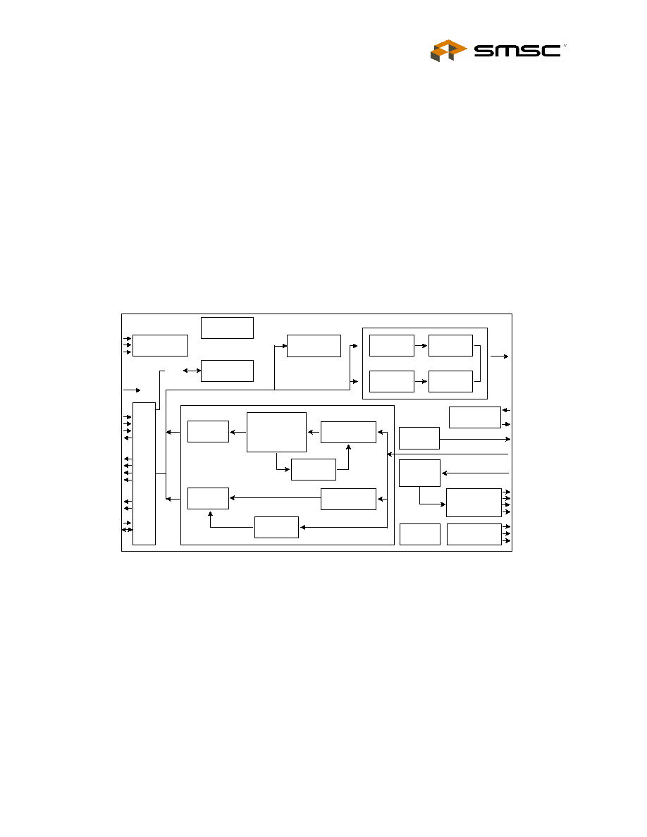
Chapter 1 General Description
The SMSC LAN83C185 is a low-power, highly integrated analog interface IC for high-performance
embedded Ethernet applications. The LAN83C185 requires only a single +3.3V supply.
The LAN83C185 consists of an encoder/decoder, scrambler/descrambler, transmitter with wave-
shaping and output driver, twisted-pair receiver with on-chip adaptive equalizer and baseline wander
(BLW) correction, clock and data recovery, and Media Independent Interface (MII).
The LAN83C185 is fully compliant with IEEE 802.3/ 802.3u standards and supports both 802.3u-
compliant and vendor-specific register functions. It contains a full-duplex 10-BASET/100BASE-TX
transceiver and supports 10-Mbps (10BASE-T) operation on Category 3 and Category 5 unshielded
twisted-pair cable, and 100-Mbps (100BASE-TX) operation on Category 5 unshielded twisted-pair
cable.
1.1
Architectural Overview
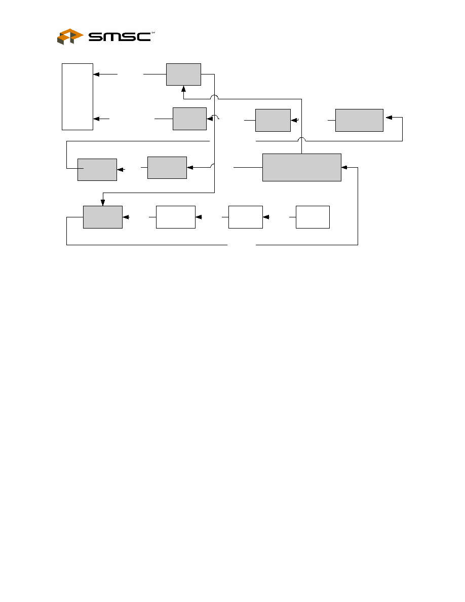
Figure 1.1 LAN83C185 Architectural Overview
10M Rx
Logic
100M Rx
Logic
DSP System:
Clock
Data Recovery
Equalizer
Analog-to-
Digital
100M PLL
Squelch &
Filters
10M PLL
Receive Section
Central
Bias
Auto-
Negotiation
Management
Control
SMI
MII
Log
ic
TXP / TXN
TXD[0..3]
TX_EN
TX_ER
TX_CLK
RXD[0..3]
RX_DV
RX_ER
RX_CLK
CRS
COL
MDC
MDIO
SPEED100
LINKON
ACTIVITY
FDUPLEX
LED Circuitry
GPO Circuitry
MODE Control
GPO0
GPO1
GPO2
nINT
nRESET
RXP / RXN
10M Tx
Logic
10M
Transmitter
100M Tx
Logic
100M
Transmitter
Transmit Section
PLL
XTAL1
XTAL2
MODE0
MODE1
MODE2
PHY
Address
Latches
PHYAD[0..4]
1.8V
Regulator
Interrupt
Generator

High Performance Single Chip Low Power 10/100 Ethernet Physical Layer Transceiver (PHY)
Datasheet
Rev. 0.8 (11-16-04)
10
SMSC LAN83C185
DATASHEET
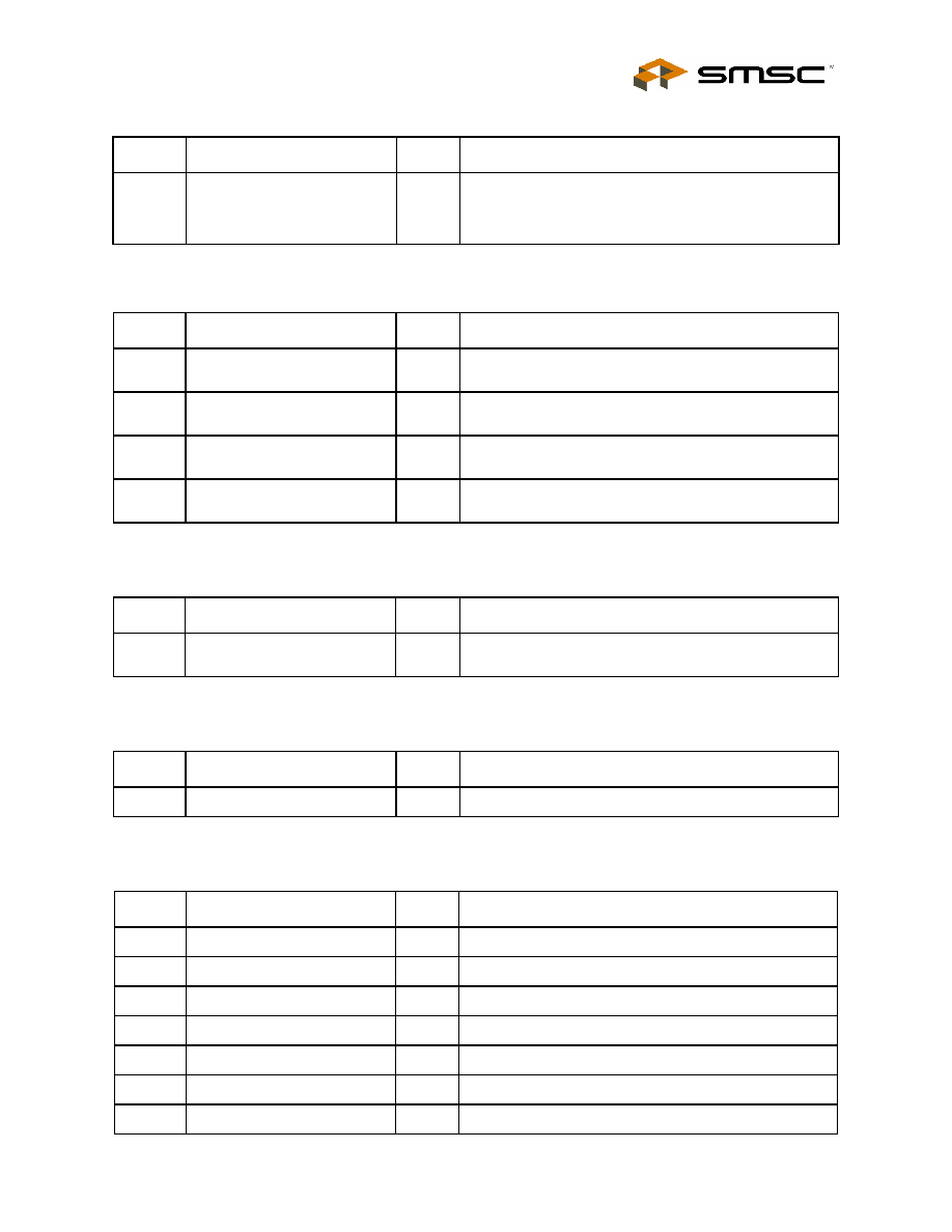
Chapter 2 Pin Configuration
Figure 2.1 Package Pinout
LAN83C185
64
63
62
61
60
59
58
57
56
55
54
53
52
51
50
49
17
18
19
20
21
22
23
24
25
26
27
28
29
30
31
32
1
2
3
4
5
6
7
8
9
10
11
12
13
14
15
16
48
47
46
45
44
43
42
41
40
39
38
37
36
35
34
33
TXD0
TXD1
TXD2
TXD3
TX_ER/TXD4
TX_EN
TX_CLK
RXD0
RXD1
RXD2
RXD3
RX_ER/RXD4
RX_DV
RX_CLK
CRS
COL
MDC
MD
IO
TX
P
TX
N
RXP
RX
N
SPEED100/PHYAD0
LI
N
K
ON/
P
HYA
D
1
ACTI
VI
TY/
P
H
Y
A
D
2
F
D
U
P
L
E
X
/
PH
YA
D
3
GPO1/PHYAD4
MODE0
MODE1
MODE2
TEST0
TEST1
CLK_FREQ
REG_EN
GPO0/MII
GPO2
nINT
nR
S
T
CL
K
I
N/
X
T
A
L
1
XT
A
L
2
NC
1
EX
R
E
S
1
NC
2
AVD
D
1
AVD
D
2
AVD
D
3
AVD
D
4
AV
SS
1
AV
SS
2
AV
SS
3
AV
SS
4
AV
SS
5
VREG
VDD_CORE
VDD1
VD
D
2
VDD3
VSS1
VS
S3
VS
S4
VS
S5
VSS6
VSS7
VSS2

High Performance Single Chip Low Power 10/100 Ethernet Physical Layer Transceiver (PHY)
Datasheet
SMSC LAN83C185
11
Rev. 0.8 (11-16-04)
DATASHEET
Table 2.1 LAN83C185 64-PIN TQFP Pinout
PIN NO.
PIN NAME
PIN NO.
PIN NAME
1
GPO0/MII
33
RX_DV
2
GPO1/PHYAD4
34
RX_CLK
3
GPO2
35
RX_ER/RXD4
4
MODE0
36
VSS6
5
MODE1
37
TX_ER/TXD4
6
MODE2
38
TX_CLK
7
VSS1
39
TX_EN
8
VDD1
40
VSS7
9
TEST0
41
TXD0
10
TEST1
42
TXD1
11
CLK_FREQ
43
VDD3
12
REG_EN
44
TXD2
13
VREG
45
TXD3
14
VDD_CORE
46
nINT
15
VSS2
47
COL
16
SPEED100/PHYAD0
48
CRS
17
LINKON/PHYAD1
49
AVSS1
18
VDD2
50
TXN
19
ACTIVITY/PHYAD2
51
TXP
20
FDUPLEX/PHYAD3
52
AVSS2
21
VSS3
53
AVDD1
22
XTAL2
54
RXN
23
CLKIN/XTAL1
55
RXP
24
VSS4
56
NC2
25
nRST
57
AVDD2
26
MDIO
58
AVSS3
27
MDC
59
EXRES1
28
VSS5
60
AVSS4
29
RXD3
61
AVDD3
30
RXD2
62
AVSS5
31
RXD1
63
AVDD4
32
RXD0
64
NC1

High Performance Single Chip Low Power 10/100 Ethernet Physical Layer Transceiver (PHY)
Datasheet
Rev. 0.8 (11-16-04)
12
SMSC LAN83C185
DATASHEET
Chapter 3 Pin Description
This chapter describes in detail the functionality of each of the five main architectural blocks.
The term "block" defines a stand-alone entity on the floor plan of the chip.
3.1
I/O Signals
I
� Input. Digital TTL levels.
O
� Output. Digital TTL levels.
AI
� Input. Analog levels.
AO
� Output. Analog levels.
AI/O � Input or Output. Analog levels.
Note: Reset as used in the signal descriptions is defined as nRST being active low.
Configuration inputs are listed in parenthesis.
Table 3.1 MII Signals
PIN NO.
SIGNAL NAME
TYPE
DESCRIPTION
41
TXD0
I
Transmit Data 0: Bit 0 of the 4 data bits that are accepted
by the PHY for transmission.
42
TXD1
I
Transmit Data 1: Bit 1 of the 4 data bits that are accepted
by the PHY for transmission.
39
TX_EN
I
Transmit Enable: Indicates that valid data is presented
on the TXD[3:0] signals, for transmission.
35
RX_ER
(RXD4)
O
O
Receive Error: Asserted to indicate that an error was
detected somewhere in the frame presently being
transferred from the PHY.
In Symbol Interface (5B Decoding) mode, this signal is the
MII Receive Data 4: the MSB of the received 5-bit symbol
code-group.
47
COL
O
MII Collision Detect: Asserted to indicate detection of
collision condition.
32
RXD0
O
Receive Data 0: Bit 0 of the 4 data bits that are sent by
the PHY in the receive path.
31
RXD1
O
Receive Data 1: Bit 1 of the 4 data bits that are sent by
the PHY in the receive path.
44
TXD2
I
Transmit Data 2: Bit 2 of the 4 data bits that are accepted
by the PHY for transmission.
45
TXD3
I
Transmit Data 3: Bit 3 of the 4 data bits that are accepted
by the PHY for transmission.

High Performance Single Chip Low Power 10/100 Ethernet Physical Layer Transceiver (PHY)
Datasheet
SMSC LAN83C185
13
Rev. 0.8 (11-16-04)
DATASHEET
37
TX_ER
(TXD4)
I
I
MII Transmit Error: When driven high, the 4B/5B encode
process substitutes the Transmit Error code-group (/H/)
for the encoded data word. This input is ignored in
10BaseT operation.
In Symbol Interface (5B Decoding) mode, this signal
becomes the MII Transmit Data 4: the MSB of the 5-bit
symbol code-group.
48
CRS
O
Carrier Sense: Indicate detection of carrier.
33
RX_DV O
Receive Data Valid: Indicates that recovered and
decoded data nibbles are being presented on RXD[3:0].
30
RXD2
O
Receive Data 2: Bit 2 of the 4 data bits that sent by the
PHY in the receive path.
29
RXD3
O
Receive Data 3: Bit 3 of the 4 data bits that sent by the
PHY in the receive path.
38
TX_CLK
O
Transmit Clock: 25MHz in 100Base-TX mode. 2.5MHz in
10Base-T mode.
34
RX_CLK
O
Receive Clock: 25MHz in 100Base-TX mode. 2.5MHz in
10Base-T mode.
Table 3.2 LED Signals
PIN NO.
SIGNAL NAME
TYPE
DESCRIPTION
16
SPEED100
O
LED1 � SPEED100 indication. Active indicates that the
selected speed is 100Mbps. Inactive indicates that the
selected speed is 10Mbps.
17
LINKON
O
LED2 � LINK ON indication. Active indicates that the Link
(100Base-TX or 10Base-T) is on.
19
ACTIVITY
O
LED3 � ACTIVITY indication. Active indicates that there
is Carrier sense (CRS) from the active PMD.
20
FDUPLEX
O
LED4 � DUPLEX indication. Active indicates that the PHY
is in full-duplex mode.
Table 3.3 Management Signals
PIN NO.
SIGNAL NAME
TYPE
DESCRIPTION
26
MDIO
IO
Management Data Input/OUTPUT: Serial management
data input/output.
27
MDC
I
Management Clock: Serial management clock.
Table 3.1 MII Signals (continued)
PIN NO.
SIGNAL NAME
TYPE
DESCRIPTION

High Performance Single Chip Low Power 10/100 Ethernet Physical Layer Transceiver (PHY)
Datasheet
Rev. 0.8 (11-16-04)
14
SMSC LAN83C185
DATASHEET
Table 3.4 Configuration Inputs
PIN NO.
SIGNAL NAME
TYPE
DESCRIPTION
2
PHYAD4
I
PHY Address Bit 4: set the default address of the PHY.
20
PHYAD3
I
PHY Address Bit 3: set the default address of the PHY.
19
PHYAD2
I
PHY Address Bit 2: set the default address of the PHY.
17
PHYAD1
I
PHY Address Bit 1: set the default address of the PHY.
16
PHYAD0
I
PHY Address Bit 0: set the default address of the PHY.
6
MODE2
I
PHY Operating Mode Bit 2: set the default MODE of the
PHY. See
Section 5.4.9.2, "Mode Bus � MODE[2:0]," on
page 47
for the MODE options.
5
MODE1
I
PHY Operating Mode Bit 1: set the default MODE of the
PHY. See
Section 5.4.9.2, "Mode Bus � MODE[2:0]," on
page 47
for the MODE options.
4
MODE0
I
PHY Operating Mode Bit 0: set the default MODE of the
PHY. See
Section 5.4.9.2, "Mode Bus � MODE[2:0]," on
page 47
for the MODE options.
10
TEST1
I
Test Mode Select 1: Must be left floating.
9
TEST0
I
Test Mode Select 0: Must be left floating.
12
REG_EN
I
Internal +1.8V Regulator Enable:
+3.3V � Enables internal regulator.
0V � Disables internal regulator.
Table 3.5 General Signals
PIN NO.
SIGNAL NAME
TYPE
DESCRIPTION
46
nINT
OD
LAN Interrupt � Active Low output.
25
nRST
I
External Reset � input of the system reset. This signal is
active LOW.
23
CLKIN/XTAL1
I
Clock Input � 25 MHz external clock or crystal input.
22
XTAL2
O
Clock Output � 25 MHz crystal output.
11
CLK_FREQ
I
Clock Frequency � define the frequency of the input
clock CLKIN
0 � Clock frequency is 25 MHz.
1 � Reserved.
This input needs to be held low continuously, during and
after reset. This pin should be pulled-down to VSS via a
pull-down resistor.
64
NC1
No Connect
3
GPO2
O
General Purpose Output 2 � General Purpose Output
signal Driven by bits in registers 27 and 31.
2
GPO1
O
General Purpose Output 1 � General Purpose Output
signal Driven by bits in registers 27 and 31.
(Muxed with PHYAD4 signal)
High Performance Single Chip Low Power 10/100 Ethernet Physical Layer Transceiver (PHY)
Datasheet
SMSC LAN83C185
15
Rev. 0.8 (11-16-04)
DATASHEET
1
GPO0
O
General Purpose Output 0 � General Purpose Output
signal. Driven by bits in registers 27 and 31.
(Muxed with MII Select) This pin should be pulled-down
or left floating � Do Not Pull Up.
Table 3.6 10/100 Line Interface
PIN NO.
SIGNAL NAME
TYPE
DESCRIPTION
51
TXP
AO
Transmit Data: 100Base-TX or 10Base-T differential
transmit outputs to magnetics.
50
TXN AO
Transmit Data: 100Base-TX or 10Base-T differential
transmit outputs to magnetics.
55
RXP
AI
Receive Data: 100Base-TX or 10Base-T differential
receive inputs from magnetics.
54
RXN
AI
Receive Data: 100Base-TX or 10Base-T differential
receive inputs from magnetics.
Table 3.7 Analog References
PIN NO.
SIGNAL NAME
TYPE
DESCRIPTION
59
EXRES1
AI
Connects to reference resistor of value 12.4K-Ohm, 1%
connected to digital GND.
Table 3.8 Analog Test Bus
PIN NO.
SIGNAL NAME
TYPE
DESCRIPTION
56
NC2
AI/O
No Connect
Table 3.9 Power Signals
PIN NO.
SIGNAL NAME
TYPE
DESCRIPTION
53
AVDD1
Power
+3.3V Analog Power
57
AVDD2
Power
+3.3V Analog Power
61
AVDD3
Power
+3.3V Analog Power
63
AVDD4
Power
+3.3V Analog Power
49
AVSS1
Power
Analog Ground
52
AVSS2
Power
Analog Ground
58
AVSS3
Power
Analog Ground
Table 3.5 General Signals (continued)
PIN NO.
SIGNAL NAME
TYPE
DESCRIPTION

High Performance Single Chip Low Power 10/100 Ethernet Physical Layer Transceiver (PHY)
Datasheet
Rev. 0.8 (11-16-04)
16
SMSC LAN83C185
DATASHEET
60
AVSS4
Power
Analog Ground
62
AVSS5
Power
Analog Ground
13
VREG
Power
+3.3V Internal Regulator Input Voltage
14
VDD_CORE
Power
+1.8V Ring (Core voltage) - required for capacitance
connection.
8
VDD1
Power
+3.3V Digital Power
18
VDD2
Power
+3.3V Digital Power
43
VDD3
Power
+3.3V Digital Power
7
VSS1
Power
Digital Ground (GND)
15
VSS2
Power
Digital Ground (GND)
21
VSS3
Power
Digital Ground (GND)
24
VSS4
Power
Digital Ground (GND)
28
VSS5
Power
Digital Ground (GND)
36
VSS6
Power
Digital Ground (GND)
40
VSS7
Power
Digital Ground (GND)
Table 3.9 Power Signals (continued)
PIN NO.
SIGNAL NAME
TYPE
DESCRIPTION
High Performance Single Chip Low Power 10/100 Ethernet Physical Layer Transceiver (PHY)
Datasheet
SMSC LAN83C185
17
Rev. 0.8 (11-16-04)
DATASHEET
Chapter 4 Architecture Details
4.1
Top Level Functional Architecture
Functionally, the PHY can be divided into the following sections:
100Base-TX transmit and receive
10Base-T transmit and receive
MII interface to the controller
Auto-negotiation to automatically determine the best speed and duplex possible
Management Control to read status registers and write control registers
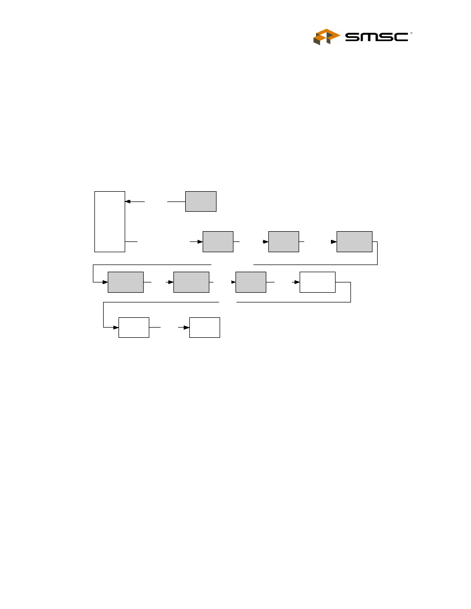
Figure 4.1
100Base-TX Data Path
4.2
100Base-TX Transmit
The data path of the 100Base-TX is shown in
Figure 4.1
. Each major block is explained below.
4.2.1
100M Transmit Data across the MII
The MAC controller drives the transmit data onto the TXD bus and asserts TX_EN to indicate valid
data. The data is latched by the PHY's MII block on the rising edge of TX_CLK. The data is in the
form of 4-bit wide 25MHz data.
4.2.2
4B/5B Encoding
The transmit data passes from the MII block to the 4B/5B encoder. This block encodes the data from
4-bit nibbles to 5-bit symbols (known as "code-groups") according to
Table 4.1
. Each 4-bit data-nibble
is mapped to 16 of the 32 possible code-groups. The remaining 16 code-groups are either used for
control information or are not valid.
The first 16 code-groups are referred to by the hexadecimal values of their corresponding data nibbles,
0 through F. The remaining code-groups are given letter designations with slashes on either side. For
example, an IDLE code-group is /I/, a transmit error code-group is /H/, etc.
MAC
Tx
Driver
MLT-3
Converter
NRZI
Converter
4B/5B
Encoder
Magnetics
CAT-5
RJ45
100M
PLL
MII 25 MHz by 4 bits
TX_CLK
(for MII)
25MHz by
5 bits
NRZI
MLT-3
MLT-3
MLT-3
MLT-3
Scrambler
and PISO
125 Mbps Serial
MII
25MHz
by 4 bits

High Performance Single Chip Low Power 10/100 Ethernet Physical Layer Transceiver (PHY)
Datasheet
Rev. 0.8 (11-16-04)
18
SMSC LAN83C185
DATASHEET
The encoding process may be bypassed by clearing bit 6 of register 31. When the encoding is
bypassed the 5
th
transmit data bit is equivalent to TX_ER.
Note that encoding can be bypassed only when the MAC interface is configured to operate in MII
mode.
Table 4.1 4B/5B Code Table
CODE
GROUP
SYM
RECEIVER
INTERPRETATION
TRANSMITTER
INTERPRETATION
11110
0
0
0000 DATA
0
0000 DATA
01001
1
1
0001
1
0001
10100
2
2
0010
2
0010
10101
3
3
0011
3
0011
01010
4
4
0100
4
0100
01011
5
5
0101
5
0101
01110
6
6 0110
6
0110
01111
7
7 0111
7
0111
10010
8
8 1000
8
1000
10011
9
9 1001
9
1001
10110
A
A 1010
A
1010
10111
B
B 1011
B
1011
11010
C
C 1100
C
1100
11011
D
D 1101
D
1101
11100
E
E 1110
E
1110
11101
F
F 1111
F
1111
11111
I
IDLE
Sent after /T/R until TX_EN
11000
J
First nibble of SSD, translated to "0101"
following IDLE, else RX_ER
Sent for rising TX_EN
10001
K
Second nibble of SSD, translated to
"0101" following J, else RX_ER
Sent for rising TX_EN
01101
T
First nibble of ESD, causes de-assertion
of CRS if followed by /R/, else assertion
of RX_ER
Sent for falling TX_EN
00111
R
Second nibble of ESD, causes
deassertion of CRS if following /T/, else
assertion of RX_ER
Sent for falling TX_EN
00100
H
Transmit Error Symbol
Sent for rising TX_ER
00110
V
INVALID, RX_ER if during RX_DV
INVALID
11001
V
INVALID, RX_ER if during RX_DV
INVALID
00000
V
INVALID, RX_ER if during RX_DV
INVALID
00001
V
INVALID, RX_ER if during RX_DV
INVALID
High Performance Single Chip Low Power 10/100 Ethernet Physical Layer Transceiver (PHY)
Datasheet
SMSC LAN83C185
19
Rev. 0.8 (11-16-04)
DATASHEET
4.2.3
Scrambling
Repeated data patterns (especially the IDLE code-group) can have power spectral densities with large
narrow-band peaks. Scrambling the data helps eliminate these peaks and spread the signal power
more uniformly over the entire channel bandwidth. This uniform spectral density is required by FCC
regulations to prevent excessive EMI from being radiated by the physical wiring.
The seed for the scrambler is generated from the PHY address, PHYAD[4:0], ensuring that in multiple-
PHY applications, such as repeaters or switches, each PHY will have its own scrambler sequence.
The scrambler also performs the Parallel In Serial Out conversion (PISO) of the data.
4.2.4
NRZI and MLT3 Encoding
The scrambler block passes the 5-bit wide parallel data to the NRZI converter where it becomes a
serial 125MHz NRZI data stream. The NRZI is encoded to MLT-3. MLT3 is a tri-level code where a
change in the logic level represents a code bit "1" and the logic output remaining at the same level
represents a code bit "0".
4.2.5
100M Transmit Driver
The MLT3 data is then passed to the analog transmitter, which launches the differential MLT-3 signal,
on outputs TXP and TXN, to the twisted pair media via a 1:1 ratio isolation transformer. The 10Base-
T and 100Base-TX signals pass through the same transformer so that common "magnetics" can be
used for both. The transmitter drives into the 100
impedance of the CAT-5 cable. Cable termination
and impedance matching require external components.
4.2.6
100M Phase Lock Loop (PLL)
The 100M PLL locks onto reference clock and generates the 125MHz clock used to drive the 125 MHz
logic and the 100Base-Tx Transmitter.
00010
V
INVALID, RX_ER if during RX_DV
INVALID
00011
V
INVALID, RX_ER if during RX_DV
INVALID
00101
V
INVALID, RX_ER if during RX_DV
INVALID
01000
V
INVALID, RX_ER if during RX_DV
INVALID
01100
V
INVALID, RX_ER if during RX_DV
INVALID
10000
V
INVALID, RX_ER if during RX_DV
INVALID
Table 4.1 4B/5B Code Table (continued)
CODE
GROUP
SYM
RECEIVER
INTERPRETATION
TRANSMITTER
INTERPRETATION
High Performance Single Chip Low Power 10/100 Ethernet Physical Layer Transceiver (PHY)
Datasheet
Rev. 0.8 (11-16-04)
20
SMSC LAN83C185
DATASHEET
Figure 4.2 Receive Data Path
4.3
100Base-TX Receive
The receive data path is shown in
Figure 4.2
. Detailed descriptions are given below.
4.3.1
100M Receive Input
The MLT-3 from the cable is fed into the PHY (on inputs RXP and RXN) via a 1:1 ratio transformer.
The ADC samples the incoming differential signal at a rate of 125M samples per second. Using a 64-
level quanitizer it generates 6 digital bits to represent each sample. The DSP adjusts the gain of the
ADC according to the observed signal levels such that the full dynamic range of the ADC can be used.
4.3.2
Equalizer, Baseline Wander Correction and Clock and Data Recovery
The 6 bits from the ADC are fed into the DSP block. The equalizer in the DSP section compensates
for phase and amplitude distortion caused by the physical channel consisting of magnetics, connectors,
and CAT- 5 cable. The equalizer can restore the signal for any good-quality CAT-5 cable between 1m
and 150m.
If the DC content of the signal is such that the low-frequency components fall below the low frequency
pole of the isolation transformer, then the droop characteristics of the transformer will become
significant and Baseline Wander (BLW) on the received signal will result. To prevent corruption of the
received data, the PHY corrects for BLW and can receive the ANSI X3.263-1995 FDDI TP-PMD
defined "killer packet" with no bit errors.
The 100M PLL generates multiple phases of the 125MHz clock. A multiplexer, controlled by the timing
unit of the DSP, selects the optimum phase for sampling the data. This is used as the received
recovered clock. This clock is used to extract the serial data from the received signal.
4.3.3
NRZI and MLT-3 Decoding
The DSP generates the MLT-3 recovered levels that are fed to the MLT-3 converter. The MLT-3 is then
converted to an NRZI data stream.
MAC
A/D
Converter
MLT-3
Converter
NRZI
Converter
4B/5B
Decoder
Magnetics
CAT-5
RJ45
100M
PLL
MII 25MHz by 4
bits
RX_CLK
25MHz by
5 bits
NRZI
MLT-3
MLT-3
MLT-3
6 bit Data
Descrambler
and SIPO
125 Mbps Serial
DSP: Timing
recovery, Equalizer
and BLW Correction
MLT-3
MII
25MHz
by 4 bits
High Performance Single Chip Low Power 10/100 Ethernet Physical Layer Transceiver (PHY)
Datasheet
SMSC LAN83C185
21
Rev. 0.8 (11-16-04)
DATASHEET
4.3.4
Descrambling
The descrambler performs an inverse function to the scrambler in the transmitter and also performs
the Serial In Parallel Out (SIPO) conversion of the data.
During reception of IDLE (/I/) symbols. the descrambler synchronizes its descrambler key to the
incoming stream. Once synchronization is achieved, the descrambler locks on this key and is able to
descramble incoming data.
Special logic in the descrambler ensures synchronization with the remote PHY by searching for IDLE
symbols within a window of 4000 bytes (40us). This window ensures that a maximum packet size of
1514 bytes, allowed by the IEEE 802.3 standard, can be received with no interference. If no IDLE-
symbols are detected within this time-period, receive operation is aborted and the descrambler re-starts
the synchronization process.
The descrambler can be bypassed by setting bit 0 of register 31.
4.3.5
Alignment
The de-scrambled signal is then aligned into 5-bit code-groups by recognizing the /J/K/ Start-of-Stream
Delimiter (SSD) pair at the start of a packet. Once the code-word alignment is determined, it is stored
and utilized until the next start of frame.
4.3.6
5B/4B Decoding
The 5-bit code-groups are translated into 4-bit data nibbles according to the 4B/5B table. The
translated data is presented on the RXD[3:0] signal lines. The SSD, /J/K/, is translated to "0101 0101"
as the first 2 nibbles of the MAC preamble. Reception of the SSD causes the PHY to assert the RX_DV
signal, indicating that valid data is available on the RXD bus. Successive valid code-groups are
translated to data nibbles. Reception of either the End of Stream Delimiter (ESD) consisting of the /T/R/
symbols, or at least two /I/ symbols causes the PHY to de-assert carrier sense and RX_DV.
These symbols are not translated into data.
The decoding process may be bypassed by clearing bit 6 of register 31. When the decoding is
bypassed the 5
th
receive data bit is driven out on RX_ER/RXD4. Decoding may be bypassed only
when the MAC interface is in MII mode.
4.3.7
Receive Data Valid Signal
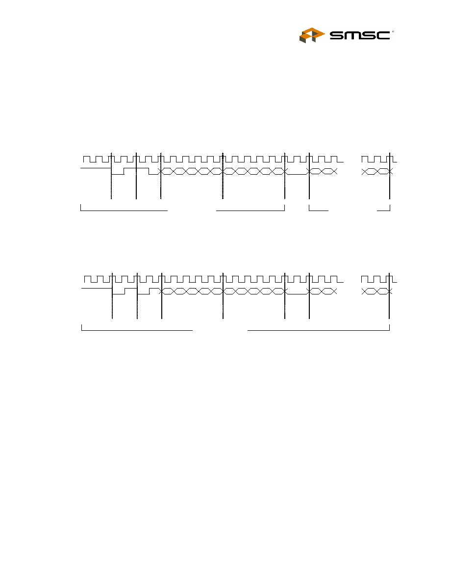
The Receive Data Valid signal (RX_DV) indicates that recovered and decoded nibbles are being
presented on the RXD[3:0] outputs synchronous to RX_CLK. RX_DV becomes active after the /J/K/
delimiter has been recognized and RXD is aligned to nibble boundaries. It remains active until either
the /T/R/ delimiter is recognized or link test indicates failure or SIGDET becomes false.
RX_DV is asserted when the first nibble of translated /J/K/ is ready for transfer over the Media
Independent Interface (MII).
Figure 4.3 Relationship Between Received Data and Some MII Signals
5
D
5
data data data data
RXD
RX_DV
RX_CLK
5
D
5
data data data data
CLEAR-TEXT
5
J
K
5
5
5
T
R
Idle

High Performance Single Chip Low Power 10/100 Ethernet Physical Layer Transceiver (PHY)
Datasheet
Rev. 0.8 (11-16-04)
22
SMSC LAN83C185
DATASHEET
4.3.8
Receiver Errors
During a frame, unexpected code-groups are considered receive errors. Expected code groups are the
DATA set (0 through F), and the /T/R/ (ESD) symbol pair. When a receive error occurs, the RX_ER
signal is asserted and arbitrary data is driven onto the RXD[3:0] lines. Should an error be detected
during the time that the /J/K/ delimiter is being decoded (bad SSD error), RX_ER is asserted true and
the value `1110' is driven onto the RXD[3:0] lines. Note that the Valid Data signal is not yet asserted
when the bad SSD error occurs.
4.3.9
100M Receive Data across the MII
The 4-bit data nibbles are sent to the MII block. These data nibbles are clocked to the controller at a
rate of 25MHz. The controller samples the data on the rising edge of RX_CLK. To ensure that the
setup and hold requirements are met, the nibbles are clocked out of the PHY on the falling edge of
RX_CLK. RX_CLK is the 25MHz output clock for the MII bus. It is recovered from the received data
to clock the RXD bus. If there is no received signal, it is derived from the system reference clock
(CLKIN).
When tracking the received data, RX_CLK has a maximum jitter of 0.8ns (provided that the jitter of the
input clock, CLKIN, is below 100ps).
4.4
10Base-T Transmit
Data to be transmitted comes from the MAC layer controller. The 10Base-T transmitter receives 4-bit
nibbles from the MII at a rate of 2.5MHz and converts them to a 10Mbps serial data stream. The data
stream is then Manchester-encoded and sent to the analog transmitter, which drives a signal onto the
twisted pair via the external magnetics.
The 10M transmitter uses the following blocks:
MII (digital)
TX 10M (digital)
10M Transmitter (analog)
10M PLL (analog)
4.4.1
10M Transmit Data across the MII
The MAC controller drives the transmit data onto the TXD BUS. When the controller has driven TX_EN
high to indicate valid data, the data is latched by the MII block on the rising edge of TX_CLK. The data
is in the form of 4-bit wide 2.5MHz data.
In order to comply with legacy 10Base-T MAC/Controllers, in Half-duplex mode the PHY loops back
the transmitted data, on the receive path. This does not confuse the MAC/Controller since the COL
signal is not asserted during this time. The PHY also supports the SQE (Heartbeat) signal. See
Section
5.4.2, "Collision Detect," on page 44
for more details.
4.4.2
Manchester Encoding
The 4-bit wide data is sent to the TX10M block. The nibbles are converted to a 10Mbps serial NRZI
data stream. The 10M PLL locks onto the external clock or internal oscillator and produces a 20MHz
clock. This is used to Manchester encode the NRZ data stream. When no data is being transmitted
(TX_EN is low, the TX10M block outputs Normal Link Pulses (NLPs) to maintain communications with
the remote link partner.
4.4.3
10M Transmit Drivers
The Manchester encoded data is sent to the analog transmitter where it is shaped and filtered before
being driven out as a differential signal across the TXP and TXN outputs.

High Performance Single Chip Low Power 10/100 Ethernet Physical Layer Transceiver (PHY)
Datasheet
SMSC LAN83C185
23
Rev. 0.8 (11-16-04)
DATASHEET
4.5
10Base-T Receive
The 10Base-T receiver gets the Manchester- encoded analog signal from the cable via the magnetics.
It recovers the receive clock from the signal and uses this clock to recover the NRZI data stream. This
10M serial data is converted to 4-bit data nibbles which are passed to the controller across the MII at
a rate of 2.5MHz.
This 10M receiver uses the following blocks:
Filter and SQUELCH (analog)
10M PLL (analog)
RX 10M (digital)
MII (digital)
4.5.1
10M Receive Input and Squelch
The Manchester signal from the cable is fed into the PHY (on inputs RXP and RXN) via 1:1 ratio
magnetics. It is first filtered to reduce any out-of-band noise. It then passes through a SQUELCH
circuit. The SQUELCH is a set of amplitude and timing comparators that normally reject differential
voltage levels below 300mV and detect and recognize differential voltages above 585mV.
4.5.2
Manchester Decoding
The output of the SQUELCH goes to the RX10M block where it is validated as Manchester encoded
data. The polarity of the signal is also checked. If the polarity is reversed (local RXP is connected to
RXN of the remote partner and vice versa), then this is identified and corrected. The reversed condition
is indicated by the flag "XPOL", bit 4 in register 27. The 10M PLL is locked onto the received
Manchester signal and from this, generates the received 20MHz clock. Using this clock, the
Manchester encoded data is extracted and converted to a 10MHz NRZI data stream. It is then
converted from serial to 4-bit wide parallel data.
The RX10M block also detects valid 10Base-T IDLE signals - Normal Link Pulses (NLPs) - to maintain
the link.
4.5.3
10M Receive Data across the MII
The 4 bit data nibbles are sent to the MII block. In MII mode, these data nibbles are valid on the rising
edge of the 2.5 MHz RX_CLK.
4.5.4
Jabber detection
Jabber is a condition in which a station transmits for a period of time longer than the maximum
permissible packet length, usually due to a fault condition, that results in holding the TX_EN input for
a long period. Special logic is used to detect the jabber state and abort the transmission to the line,
within 45ms. Once TX_EN is deasserted, the logic resets the jabber condition.
Bit 1.1 indicates that a jabber condition was detected.
4.6
MAC Interface
The MII (Media Independent Interface) block is responsible for the communication with the controller.
Special sets of hand-shake signals are used to indicate that valid received/transmitted data is present
on the 4 bit receive/transmit bus.

High Performance Single Chip Low Power 10/100 Ethernet Physical Layer Transceiver (PHY)
Datasheet
Rev. 0.8 (11-16-04)
24
SMSC LAN83C185
DATASHEET
4.6.1
MII
The MII includes 16 interface signals:
transmit data - TXD[3:0]
transmit strobe - TX_EN
transmit clock - TX_CLK
transmit error - TX_ER/TXD4
receive data - RXD[3:0]
receive strobe - RX_DV
receive clock - RX_CLK
receive error - RX_ER/RXD4
collision indication - COL
carrier sense - CRS
In MII mode, on the transmit path, the PHY drives the transmit clock, TX_CLK, to the controller. The
controller synchronizes the transmit data to the rising edge of TX_CLK. The controller drives TX_EN
high to indicate valid transmit data. The controller drives TX_ER high when a transmit error is detected.
On the receive path, the PHY drives both the receive data, RXD[3:0], and the RX_CLK signal. The
controller clocks in the receive data on the rising edge of RX_CLK when the PHY drives RX_DV high.
The PHY drives RX_ER high when a receive error is detected.
4.7
Auto-negotiation
The purpose of the Auto-negotiation function is to automatically configure the PHY to the optimum link
parameters based on the capabilities of its link partner. Auto-negotiation is a mechanism for
exchanging configuration information between two link-partners and automatically selecting the highest
performance mode of operation supported by both sides. Auto-negotiation is fully defined in clause 28
of the IEEE 802.3 specification.
Once auto-negotiation has completed, information about the resolved link can be passed back to the
controller via the Serial Management Interface (SMI). The results of the negotiation process are
reflected in the Speed Indication bits in register 31, as well as the Link Partner Ability Register
(Register 5).
The auto-negotiation protocol is a purely physical layer activity and proceeds independently of the MAC
controller.
The advertised capabilities of the PHY are stored in register 4 of the SMI registers. The default
advertised by the PHY is determined by user-defined on-chip signal options.
The following blocks are activated during an Auto-negotiation session:
Auto-negotiation (digital)
100M ADC (analog)
100M PLL (analog)
100M equalizer/BLW/clock recovery (DSP)
10M SQUELCH (analog)
10M PLL (analog)
10M Transmitter (analog)
When enabled, auto-negotiation is started by the occurrence of one of the following events:
Hardware reset
Software reset

High Performance Single Chip Low Power 10/100 Ethernet Physical Layer Transceiver (PHY)
Datasheet
SMSC LAN83C185
25
Rev. 0.8 (11-16-04)
DATASHEET
Power-down reset
Link status down
Setting register 0, bit 9 high (auto-negotiation restart)
On detection of one of these events, the PHY begins auto-negotiation by transmitting bursts of Fast
Link Pulses (FLP). These are bursts of link pulses from the 10M transmitter. They are shaped as
Normal Link Pulses and can pass uncorrupted down CAT-3 or CAT-5 cable. A Fast Link Pulse Burst
consists of up to 33 pulses. The 17 odd-numbered pulses, which are always present, frame the FLP
burst. The 16 even-numbered pulses, which may be present or absent, contain the data word being
transmitted. Presence of a data pulse represents a "1", while absence represents a "0".
The data transmitted by an FLP burst is known as a "Link Code Word." These are defined fully in IEEE
802.3 clause 28. In summary, the PHY advertises 802.3 compliance in its selector field (the first 5 bits
of the Link Code Word). It advertises its technology ability according to the bits set in register 4 of the
SMI registers.
There are 4 possible matches of the technology abilities. In the order of priority these are:
100M Full Duplex (Highest priority)
100M Half Duplex
10M Full Duplex
10M Half Duplex
If the full capabilities of the PHY are advertised (100M, Full Duplex), and if the link partner is capable
of 10M and 100M, then auto-negotiation selects 100M as the highest performance mode. If the link
partner is capable of Half and Full duplex modes, then auto-negotiation selects Full Duplex as the
highest performance operation.
Once a capability match has been determined, the link code words are repeated with the acknowledge
bit set. Any difference in the main content of the link code words at this time will cause auto-negotiation
to re-start. Auto-negotiation will also re-start if not all of the required FLP bursts are received.
The capabilities advertised during auto-negotiation by the PHY are initially determined by the logic
levels latched on the MODE[2:0] bus after reset completes. This bus can also be used to disable auto-
negotiation on power-up.
Writing register 4 bits [8:5] allows software control of the capabilities advertised by the PHY. Writing
register 4 does not automatically re-start auto-negotiation. Register 0, bit 9 must be set before the new
abilities will be advertised. Auto-negotiation can also be disabled via software by clearing register 0,
bit 12.
The LAN83C185 does not support "Next Page" capability.
4.7.1
Parallel Detection
If the LAN83C185 is connected to a device lacking the ability to auto-negotiate (i.e. no FLPs are
detected), it is able to determine the speed of the link based on either 100M MLT-3 symbols or 10M
Normal Link Pulses. In this case the link is presumed to be Half Duplex per the IEEE standard. This
ability is known as "Parallel Detection. This feature ensures interoperability with legacy link partners.
If a link is formed via parallel detection, then bit 0 in register 6 is cleared to indicate that the Link
Partner is not capable of auto-negotiation. The controller has access to this information via the
management interface. If a fault occurs during parallel detection, bit 4 of register 6 is set.
Register 5 is used to store the Link Partner Ability information, which is coded in the received FLPs.
If the Link Partner is not auto-negotiation capable, then register 5 is updated after completion of parallel
detection to reflect the speed capability of the Link Partner.

High Performance Single Chip Low Power 10/100 Ethernet Physical Layer Transceiver (PHY)
Datasheet
Rev. 0.8 (11-16-04)
26
SMSC LAN83C185
DATASHEET
4.7.2
Re-starting Auto-negotiation
Auto-negotiation can be re-started at any time by setting register 0, bit 9. Auto-negotiation will also re-
start if the link is broken at any time. A broken link is caused by signal loss. This may occur because
of a cable break, or because of an interruption in the signal transmitted by the Link Partner. Auto-
negotiation resumes in an attempt to determine the new link configuration.
If the management entity re-starts Auto-negotiation by writing to bit 9 of the control register, the
LAN83C185 will respond by stopping all transmission/receiving operations. Once the break_link_timer
is done, in the Auto-negotiation state-machine (approximately 1200ms) the auto-negotiation will re-
start. The Link Partner will have also dropped the link due to lack of a received signal, so it too will
resume auto-negotiation.
4.7.3
Disabling Auto-negotiation
Auto-negotiation can be disabled by setting register 0, bit 12 to zero. The device will then force its
speed of operation to reflect the information in register 0, bit 13 (speed) and register 0, bit 8 (duplex).
The speed and duplex bits in register 0 should be ignored when auto-negotiation is enabled.
4.7.4
Half vs. Full Duplex
Half Duplex operation relies on the CSMA/CD (Carrier Sense Multiple Access / Collision Detect)
protocol to handle network traffic and collisions. In this mode, the carrier sense signal, CRS, responds
to both transmit and receive activity. In this mode, If data is received while the PHY is transmitting,
a collision results.
In Full Duplex mode, the PHY is able to transmit and receive data simultaneously. In this mode, CRS
responds only to receive activity. The CSMA/CD protocol does not apply and collision detection is
disabled.
4.8
PHY Management Control
The Management Control module includes 3 blocks:
Serial Management Interface (SMI)
Management Registers Set
Interrupt
4.8.1
Serial Management Interface (SMI)
The Serial Management Interface is used to control the LAN83C185 and obtain its status. This
interface supports registers 0 through 6 as required by Clause 22 of the 802.3 standard, as well as
"vendor-specific" registers 16 to 31 allowed by the specification. Non-supported registers (7 to 15) will
be read as hexadecimal "FFFF".
At the system level there are 2 signals, MDIO and MDC where MDIO is bi-directional open-drain and
MDC is the clock.
A special feature (enabled by register 17 bit 3) forces the PHY to disregard the PHY-Address in the
SMI packet causing the PHY to respond to any address. This feature is useful in multi-PHY
applications and in production testing, where the same register can be written in all the PHYs using a
single write transaction.
The MDC signal is an aperiodic clock provided by the station management controller (SMC). The MDIO
signal receives serial data (commands) from the controller SMC, and sends serial data (status) to
the SMC. The minimum time between edges of the MDC is 160 ns. There is no maximum time
between edges.
High Performance Single Chip Low Power 10/100 Ethernet Physical Layer Transceiver (PHY)
Datasheet
SMSC LAN83C185
27
Rev. 0.8 (11-16-04)
DATASHEET
The minimum cycle time (time between two consecutive rising or two consecutive falling edges) is 400
ns. These modest timing requirements allow this interface to be easily driven by the I/O port of a
microcontroller.
The data on the MDIO line is latched on the rising edge of the MDC. The frame structure and timing
of the data is shown in
Figure 4.4
and
Figure 4.5
.
The timing relationships of the MDIO signals are further described in
Section 6.1, "Serial
Management Interface (SMI) Timing," on page 51
.
Figure 4.4 MDIO Timing and Frame Structure - READ Cycle
Figure 4.5 MDIO Timing and Frame Structure - WRITE Cycle
MDC
MDI0
Read Cycle
...
32 1's
0
1
1
0
A4 A3 A2 A1 A0 R4 R3 R2 R1 R0
D1
...
D15
D14
D0
Preamble
Start of
Frame
OP
Code
PHY Address
Register Address
Turn
Around
Data
Data From Phy
Data To Phy
MDC
MDIO
...
32 1's
0
1
1
0
A4 A3 A2 A1 A0 R4 R3 R2 R1 R0
Write Cycle
D15
D14
D1
D0
...
Data
Preamble
Start of
Frame
OP
Code
PHY Address
Register Address
Turn
Around
Data To Phy

High Perfor
mance Single Chip Low
Power 10
/100
Ethern
e
t Physical Layer T
r
ansceiver (
P
HY)
Dat
ashe
e
t
Rev
.
0.8 (
1
1-16
-04)
28
SMSC LAN8
3C185
DA
T
ASHEET
Chapter 5 Registers
Table 5.1 Control Register: Register 0 (Basic)
15
14
13
12
11
10
9
8
7
6
5
4
3
2
1
0
Reset
Loopback
Speed Select
A/N Enable
Power Down
Isolate
Restart A/N
Duplex Mode
Collision Test
Reserved
Table 5.2 Status Register: Register 1 (Basic)
15
14
13
12
11
10
9
8
7
6
5
4
3
2
1
0
100Base-
T4
100Base-
TX
Full Duplex
100Base-
TX
Half
Duplex
10Base-T
Full
Duplex
10Base-T
Half
Duplex
Reserved
A/N
Complete
Remote
Fault
A/N
Ability
Link
Status
Jabber
Detect
Extended
Capability
Table 5.3 PHY ID 1 Register: Register 2 (Extended)
15
14
13
12
11
10
9
8
7
6
5
4
3
2
1
0
PHY ID Number (Bits 3-18 of the Organizationally Unique Identifier - OUI)
Table 5.4 PHY ID 2 Register: Register 3 (Extended)
15
14
13
12
11
10
9
8
7
6
5
4
3
2
1
0
PHY ID Number (Bits 19-24 of the Organizationally Unique
Identifier - OUI)
Manufacturer Model Number
Manufacturer Revision Number
Table 5.5 Auto-Negotiation Advertisement: Register 4 (Extended)
15
14
13
12
11
10
9
8
7
6
5
4
3
2
1
0
Next
Page
Reserved
Remote
Fault
Reserved
Symmetric
Pause
Operation
Asymmetric
Pause
Operation
100Base-T4
100Base-TX
Full Duplex
100Base-
TX
10Base-T
Full
Duplex
10Base-T
IEEE 802.3 Selector Field
High Perfor
mance Single Chip Low
Power 10
/100
Ethern
e
t Physical Layer T
r
ansceiver (
P
HY)
Dat
ashe
e
t
Rev
.
0.8 (
1
1-16
-04)
29
SMSC LAN8
3C185
DA
T
ASHEET
Note: Next Page capability is not supported.
Table 5.6 Auto-Negotiation Link Partner Base Page Ability Register: Register 5 (Extended)
15
14
13
12
11
10
9
8
7
6
5
4
3
2
1
0
Next
Page
Acknowledge
Remote
Fault
Reserved
Pause
100Base-T4
100Base-TX
Full Duplex
100Base-TX
10Base-T
Full Duplex
10Base-T
IEEE 802.3 Selector Field
Table 5.7 Auto-Negotiation Expansion Register: Register 6 (Extended)
15
14
13
12
11
10
9
8
7
6
5
4
3
2
1
0
Reserved
Parallel
Detect
Fault
Link
Partner
Next Page
Able
Next Page
Able
Page
Received
Link
Partner
A/N Able
Table 5.8 Auto-Negotiation Link Partner Next Page Transmit Register: Register 7 (Extended)
15
14
13
12
11
10
9
8
7
6
5
4
3
2
1
0
Reserved
Table 5.9 Register 8 (Extended)
15
14
13
12
11
10
9
8
7
6
5
4
3
2
1
0
IEEE Reserved
Table 5.10 Register 9 (Extended)
15
14
13
12
11
10
9
8
7
6
5
4
3
2
1
0
IEEE Reserved

High Perfor
mance Single Chip Low
Power 10
/100
Ethern
e
t Physical Layer T
r
ansceiver (
P
HY)
Dat
ashe
e
t
Rev
.
0.8 (
1
1-16
-04)
30
SMSC LAN8
3C185
DA
T
ASHEET
Table 5.11 Register 10 (Extended)
15
14
13
12
11
10
9
8
7
6
5
4
3
2
1
0
IEEE Reserved
Table 5.12 Register 11 (Extended)
15
14
13
12
11
10
9
8
7
6
5
4
3
2
1
0
IEEE Reserved
Table 5.13 Register 12 (Extended)
15
14
13
12
11
10
9
8
7
6
5
4
3
2
1
0
IEEE Reserved
Table 5.14 Register 13 (Extended)
15
14
13
12
11
10
9
8
7
6
5
4
3
2
1
0
IEEE Reserved
Table 5.15 Register 14 (Extended)
15
14
13
12
11
10
9
8
7
6
5
4
3
2
1
0
IEEE Reserved
Table 5.16 Register 15 (Extended)
15
14
13
12
11
10
9
8
7
6
5
4
3
2
1
0
IEEE Reserved

High Perfor
mance Single Chip Low
Power 10
/100
Ethern
e
t Physical Layer T
r
ansceiver (
P
HY)
Dat
ashe
e
t
Rev
.
0.8 (
1
1-16
-04)
31
SMSC LAN8
3C185
DA
T
ASHEET
Table 5.17 Silicon Revision Register 16: Vendor-Specific
15
14
13
12
11
10
9
8
7
6
5
4
3
2
1
0
Reserved
Silicon Revision
Reserved
Table 5.18 Mode Control/ Status Register 17: Vendor-Specific
15
14
13
12
11
10
9
8
7
6
5
4
3
2
1
0
Reserved
FASTRIP
EDPWRDOWN
Reserved
LOWSQEN
MDPREBP
FARLOOPBACK
FASTEST
Reserved
REFCLKEN
PHYADBP
Force
Good
Link
Status
ENERGYON
Reserved
Table 5.19 Special Modes Register 18: Vendor-Specific
15
14
13
12
11
10
9
8
7
6
5
4
3
2
1
0
MIIMODE
CLKSELFREQ
DSPBP
SQBP
Reserved
PLLBP
ADCBP
MODE
PHYAD
Table 5.20 Reserved Register 19: Vendor-Specific
15
14
13
12
11
10
9
8
7
6
5
4
3
2
1
0
Reserved
Table 5.21 TSTCNTL Register 20: Vendor-Specific
15
14
13
12
11
10
9
8
7
6
5
4
3
2
1
0
READ
WRITE
Reserved
TEST
MODE
READ ADDRESS
WRITE ADDRESS

High Perfor
mance Single Chip Low
Power 10
/100
Ethern
e
t Physical Layer T
r
ansceiver (
P
HY)
Dat
ashe
e
t
Rev
.
0.8 (
1
1-16
-04)
32
SMSC LAN8
3C185
DA
T
ASHEET
Table 5.22 TSTREAD2 Register 21: Vendor-Specific
15
14
13
12
11
10
9
8
7
6
5
4
3
2
1
0
READ_DATA
Table 5.23 TSTREAD1 Register 22: Vendor-Specific
15
14
13
12
11
10
9
8
7
6
5
4
3
2
1
0
READ_DATA
Table 5.24 TSTWRITE Register 23: Vendor-Specific
15
14
13
12
11
10
9
8
7
6
5
4
3
2
1
0
WRITE_DATA
Table 5.25 Register 24: Vendor-Specific
15
14
13
12
11
10
9
8
7
6
5
4
3
2
1
0
Reserved
Table 5.26 Register 25: Vendor-Specific
15
14
13
12
11
10
9
8
7
6
5
4
3
2
1
0
Reserved
Table 5.27 Register 26: Vendor-Specific
15
14
13
12
11
10
9
8
7
6
5
4
3
2
1
0
Reserved
High Perfor
mance Single Chip Low
Power 10
/100
Ethern
e
t Physical Layer T
r
ansceiver (
P
HY)
Dat
ashe
e
t
Rev
.
0.8 (
1
1-16
-04)
33
SMSC LAN8
3C185
DA
T
ASHEET
Table 5.28 Special Control/Status Indications Register 27: Vendor-Specific
15
14
13
12
11
10
9
8
7
6
5
4
3
2
1
0
Reserved
SWRST_FAST
SQEOFF
VCOOFF_LP
Reserved
Reserved
Reserved
Reserved
Reserved
XPOL
AUTONEGS
Table 5.29 Special Internal Testability Control Register 28: Vendor-Specific
15
14
13
12
11
10
9
8
7
6
5
4
3
2
1
0
Reserved
Table 5.30 Interrupt Source Flags Register 29: Vendor-Specific
15
14
13
12
11
10
9
8
7
6
5
4
3
2
1
0
Reserved
INT7
INT6
INT5
INT4
INT3
INT2
INT1
Reserved
Table 5.31 Interrupt Mask Register 30: Vendor-Specific
15
14
13
12
11
10
9
8
7
6
5
4
3
2
1
0
Reserved
Mask Bits
Table 5.32 PHY Special Control/Status Register 31: Vendor-Specific
15
14
13
12
11
10
9
8
7
6
5
4
3
2
1
0
Reserved
Reserved
Special
Autodone
Reserved
GPO2
GPO1
GPO0
Enable
4B5B
Reserved
Speed Indication
Reserved
Scramble
Disable

High Performance Single Chip Low Power 10/100 Ethernet Physical Layer Transceiver (PHY)
Datasheet
Rev. 0.8 (11-16-04)
34
SMSC LAN83C185
DATASHEET
5.1
SMI Register Mapping
The following registers are supported (register numbers are in decimal):
5.2
SMI Register Format
The mode key is as follows:
RW = read/write,
SC = self clearing,
WO = write only,
RO = read only,
LH = latch high, clear on read of register,
LL = latch low, clear on read of register,
NASR = Not Affected by Software Reset
Table 5.33 SMI Register Mapping
REGISTER #
DESCRIPTION
GROUP
0
Basic Control Register
Basic
1
Basic Status Register
Basic
2
PHY Identifier 1
Extended
3
PHY Identifier 2
Extended
4
Auto-Negotiation Advertisement Register
Extended
5
Auto-Negotiation Link Partner Ability Register
Extended
6
Auto-Negotiation Expansion Register
Extended
16
Silicon Revision Register
Vendor-specific
17
Mode Control/Status Register
Vendor-specific
18
Special Modes
Vendor-specific
20
TSTCNTL � Testability/Configuration Control
Vendor-specific
21
TSTREAD1 � Testability data Read for LSB
Vendor-specific
22
TSTREAD2 � Testability data Read for MSB
Vendor-specific
23
TSTWRITE � Testability/Configuration data Write
Vendor-specific
27
Control / Status Indication Register
Vendor-specific
28
Special internal testability controls
Vendor-specific
29
Interrupt Source Register
Vendor-specific
30
Interrupt Mask Register
Vendor-specific
31
PHY Special Control/Status Register
Vendor-specific

High Performance Single Chip Low Power 10/100 Ethernet Physical Layer Transceiver (PHY)
Datasheet
SMSC LAN83C185
35
Rev. 0.8 (11-16-04)
DATASHEET
Table 5.34 Register 0 - Basic Control
ADDRESS
NAME
DESCRIPTION
MODE
DEFAULT
0.15
Reset
1 = software reset. Bit is self-clearing. For best results,
when setting this bit do not set other bits in this
register.
RW/
SC
0
0.14
Loopback
1 = loopback mode,
0 = normal operation
RW
0
0.13
Speed Select
1 = 100Mbps,
0 = 10Mbps.
Ignored if Auto Negotiation is enabled (0.12 = 1).
RW
Set by
MODE[2:0]
bus
0.12
Auto-
Negotiation
Enable
1 = enable auto-negotiate process
(overrides 0.13 and 0.8)
0 = disable auto-negotiate process
RW
Set by
MODE[2:0]
bus
0.11
Power Down
1 = General power down mode,
0 = normal operation
RW
0
0.10
Isolate
1 = electrical isolation of PHY from MII
0 = normal operation
RW
Set by
MODE[2:0]
bus
0.9
Restart Auto-
Negotiate
1 = restart auto-negotiate process
0 = normal operation. Bit is self-clearing.
RW/
SC
0
0.8
Duplex Mode
1 = Full duplex,
0 = Half duplex.
Ignored if Auto Negotiation is enabled (0.12 = 1).
RW
Set by
MODE[2:0]
bus
0.7
Collision Test
1 = enable COL test,
0 = disable COL test
RW
0
0.6:0
Reserved
RO
0
Table 5.35 Register 1 - Basic Status
ADDRESS
NAME
DESCRIPTION
MODE
DEFAULT
1.15
100Base-T4
1 = T4 able,
0 = no T4 ability
RO
0
1.14
100Base-TX Full
Duplex
1 = TX with full duplex,
0 = no TX full duplex ability
RO
1
1.13
100Base-TX Half
Duplex
1 = TX with half duplex,
0 = no TX half duplex ability
RO
1
1.12
10Base-T Full
Duplex
1 = 10Mbps with full duplex
0 = no 10Mbps with full duplex ability
RO
1
1.11
10Base-T Half
Duplex
1 = 10Mbps with half duplex
0 = no 10Mbps with half duplex ability
RO
1
1.10:6
Reserved
1.5
Auto-Negotiate
Complete
1 = auto-negotiate process completed
0 = auto-negotiate process not completed
RO
0
1.4
Remote Fault
1 = remote fault condition detected
0 = no remote fault
RO/
LH
0

High Performance Single Chip Low Power 10/100 Ethernet Physical Layer Transceiver (PHY)
Datasheet
Rev. 0.8 (11-16-04)
36
SMSC LAN83C185
DATASHEET
1.3
Auto-Negotiate
Ability
1 = able to perform auto-negotiation function
0 = unable to perform auto-negotiation function
RO
1
1.2
Link Status
1 = link is up,
0 = link is down
RO/
LL
0
1.1
Jabber Detect
1 = jabber condition detected
0 = no jabber condition detected
RO/
LH
0
1.0
Extended
Capabilities
1 = supports extended capabilities registers
0 = does not support extended capabilities registers
RO
1
Table 5.36 Register 2 - PHY Identifier 1
ADDRESS
NAME
DESCRIPTION
MODE
DEFAULT
2.15:0
PHY ID Number
Assigned to the 3rd through 18th bits of the
Organizationally Unique Identifier (OUI), respectively.
OUI=00800Fh
RW
0007h
Table 5.37 Register 3 - PHY Identifier 2
ADDRESS
NAME
DESCRIPTION
MODE
DEFAULT
3.15:10
PHY ID Number
Assigned to the 19
th
through 24
th
bits of the OUI.
RW
C0h
3.9:4
Model Number
Six-bit manufacturer's model number.
RW
0Ah
3.3:0
Revision Number
Four-bit manufacturer's revision number.
RW
1h
Table 5.38 Register 4 - Auto Negotiation Advertisement
ADDRESS
NAME
DESCRIPTION
MODE
DEFAULT
4.15
Next Page
1 = next page capable,
0 = no next page ability
This Phy does not support next page ability.
RO
0
4.14
Reserved
RO
0
4.13
Remote Fault
1 = remote fault detected,
0 = no remote fault
RW
0
4.12
Reserved
4.11:10
Pause Operation
00 = No PAUSE
01 = Asymmetric PAUSE toward link partner
10 = Symmetric PAUSE
11 = Both Symmetric PAUSE and Asymmetric
PAUSE toward local device
R/W
00
4.9
100Base-T4
1 = T4 able,
0 = no T4 ability
This Phy does not support 100Base-T4.
RO
0
Table 5.35 Register 1 - Basic Status (continued)
ADDRESS
NAME
DESCRIPTION
MODE
DEFAULT

High Performance Single Chip Low Power 10/100 Ethernet Physical Layer Transceiver (PHY)
Datasheet
SMSC LAN83C185
37
Rev. 0.8 (11-16-04)
DATASHEET
4.8
100Base-TX Full
Duplex
1 = TX with full duplex,
0 = no TX full duplex ability
RW
Set by
MODE[2:0]
bus
4.7
100Base-TX
1 = TX able,
0 = no TX ability
RW
1
4.6
10Base-T Full
Duplex
1 = 10Mbps with full duplex
0 = no 10Mbps with full duplex ability
RW
Set by
MODE[2:0]
bus
4.5
10Base-T
1 = 10Mbps able,
0 = no 10Mbps ability
RW
Set by
MODE[2:0]
bus
4.4:0
Selector Field
[00001] = IEEE 802.3
RW
00001
Table 5.39 Register 5 - Auto Negotiation Link Partner Ability
ADDRESS
NAME
DESCRIPTION
MODE
DEFAULT
5.15
Next Page
1 = "Next Page" capable,
0 = no "Next Page" ability
This Phy does not support next page ability.
RO
0
5.14
Acknowledge
1 = link code word received from partner
0 = link code word not yet received
RO
0
5.13
Remote Fault
1 = remote fault detected,
0 = no remote fault
RO
0
5.12:11
Reserved
RO
0
5.10
Pause Operation
1 = Pause Operation is supported by remote MAC,
0 = Pause Operation is not supported by remote MAC
RO
0
5.9
100Base-T4
1 = T4 able,
0 = no T4 ability.
This Phy does not support T4 ability.
RO
0
5.8
100Base-TX Full
Duplex
1 = TX with full duplex,
0 = no TX full duplex ability
RO
0
5.7
100Base-TX
1 = TX able,
0 = no TX ability
RO
0
5.6
10Base-T Full
Duplex
1 = 10Mbps with full duplex
0 = no 10Mbps with full duplex ability
RO
0
5.5
10Base-T
1 = 10Mbps able,
0 = no 10Mbps ability
RO
0
5.4:0
Selector Field
[00001] = IEEE 802.3
RO
00001
Table 5.38 Register 4 - Auto Negotiation Advertisement (continued)
ADDRESS
NAME
DESCRIPTION
MODE
DEFAULT

High Performance Single Chip Low Power 10/100 Ethernet Physical Layer Transceiver (PHY)
Datasheet
Rev. 0.8 (11-16-04)
38
SMSC LAN83C185
DATASHEET
Table 5.40 Register 6 - Auto Negotiation Expansion
ADDRESS
NAME
DESCRIPTION
MODE
DEFAULT
6.15:5
Reserved
RO
0
6.4
Parallel Detection
Fault
1 = fault detected by parallel detection logic
0 = no fault detected by parallel detection logic
RO/
LH
0
6.3
Link Partner Next
Page Able
1 = link partner has next page ability
0 = link partner does not have next page ability
RO
0
6.2
Next Page Able
1 = local device has next page ability
0 = local device does not have next page ability
RO
0
6.1
Page Received
1 = new page received
0 = new page not yet received
RO/
LH
0
6.0
Link Partner Auto-
Negotiation Able
1 = link partner has auto-negotiation ability
0 = link partner does not have auto-negotiation ability
RO
0
Table 5.41 Register 16 - Silicon Revision
ADDRESS
NAME
DESCRIPTION
MODE
DEFAULT
16.15:10
Reserved
RO
0
16.9:6
Silicon Revision
Four-bit silicon revision identifier.
RO
0001
16.5:0
Reserved
RO
0
Table 5.42 Register 17 - Mode Control/Status
ADDRESS
NAME
DESCRIPTION
MODE
DEFAULT
17.15
Reserved
Write as 0; ignore on read.
RW
0
17.14
FASTRIP
10Base-T fast mode:
0 = normal operation
1 = Reserved
Must be left at 0
RW,
NASR
0
17.13
EDPWRDOWN
Enable the Energy Detect Power-Down mode:
0 = Energy Detect Power-Down is disabled
1 = Energy Detect Power-Down is enabled
RW
0
17.12
Reserved
Write as 0, ignore on read
RW
0
17.11
LOWSQEN
The Low_Squelch signal is equal to LOWSQEN AND
EDPWRDOWN.
Low_Squelch = 1 implies a lower threshold
(more sensitive).
Low_Squelch = 0 implies a higher threshold
(less sensitive).
RW
0
17.10
MDPREBP
Management Data Preamble Bypass:
0 � detect SMI packets with Preamble
1 � detect SMI packets without preamble
RW
0
17.9
Reserved
Reserved
Must be left at 0
RW
0

High Performance Single Chip Low Power 10/100 Ethernet Physical Layer Transceiver (PHY)
Datasheet
SMSC LAN83C185
39
Rev. 0.8 (11-16-04)
DATASHEET
17.8
FASTEST
Auto-Negotiation Test Mode
0 = normal operation
1 = activates test mode
RW
0
17.7:5
Reserved
Write as 0, ignore on read.
17.4
Reserved
Reserved
Must be left at 0
RW
0
17.3
PHYADBP
1 = PHY disregards PHY address in SMI access
write.
RW
0
17.2
Force
Good Link Status
0 = normal operation;
1 = force 100TX- link active;
Note:
This bit should be set only during lab testing
RW
0
17.1
ENERGYON
ENERGYON � indicates whether energy is detected
on the line (see
Section 5.4.5.2, "Energy Detect
Power-Down," on page 44
); it goes to "0" if no valid
energy is detected within 256ms. Reset to "1" by
hardware reset, unaffected by SW reset.
RO
1
17.0
Reserved
Write as "0". Ignore on read.
RW
0
Table 5.43 Register 18 - Special Modes
ADDRESS
NAME
DESCRIPTION
MODE
DEFAULT
18.15:14
MIIMODE
MII Mode: set the mode of the MII:
0 � MII interface.
1 � Reserved
RW,
NASR
18.13
CLKSELFREQ
Clock In Selected Frequency. Set the requested input
clock frequency. This bit drives signal that goes to
external logic of the Phy and select the desired
frequency of the input clock:
0 � the clock frequency is 25MHz
1 � Reserved
RO,
NASR
18.12
DSPBP
DSP Bypass mode. Used only in special lab tests.
RW,
NASR
0
18.11
SQBP
SQUELCH Bypass mode.
RW,
NASR
0
18.10
Reserved
RW,
NASR
18.9
PLLBP
PLL Bypass mode.
RW,
NASR
18.8
ADCBP
ADC Bypass mode.
RW,
NASR
18.7:5
MODE
PHY Mode of operation. Refer to
Section 5.4.9.2,
"Mode Bus � MODE[2:0]," on page 47
for more
details.
RW,
NASR
Table 5.42 Register 17 - Mode Control/Status (continued)
ADDRESS
NAME
DESCRIPTION
MODE
DEFAULT

High Performance Single Chip Low Power 10/100 Ethernet Physical Layer Transceiver (PHY)
Datasheet
Rev. 0.8 (11-16-04)
40
SMSC LAN83C185
DATASHEET
18.4:0
PHYAD
PHY Address.
The PHY Address is used for the SMI address and for
the initialization of the Cipher (Scrambler) key. Refer
to
Section 5.4.9.1, "Physical Address Bus -
PHYAD[4:0]," on page 46
for more details.
RW,
NASR
PHYAD
Table 5.44 Register 20 - TSTCNTL
ADDRESS
NAME
DESCRIPTION
MODE
DEFAULT
20.15
READ
When setting this bit to "1", the content of the register
that is selected by the READ ADDRESS will be
latched to the TSTREAD1/2 registers. This bit is self-
cleared.
RW
0
20.14
WRITE
When setting this bit to "1", the register that is selected
by the WRITE ADDRESS is going to be written with
the data from the TSTWRITE register. This bit is self-
cleared.
RW
0
20.13:11
Reserved
20.10
TEST MODE
Enable the Testability/Configuration mode:
0 - Testability/Configuration mode disabled
1 - Testability/Configuration mode enabled
RW
0
20.9:5
READ
ADDRESS
The address of the Testability/Configuration register
that will be latched into the TSTREAD1 and
TSTREAD2 registers
RW
0
20.4:0
WRITE
ADDRESS
The address of the Testability/Configuration register
that will be written.
RW
0
Table 5.45 Register 21 - TSTREAD1
ADDRESS
NAME
DESCRIPTION
MODE
DEFAULT
21.15:0
READ_DATA
When reading registers with a size of less then 16
bits, this register contain the register data, starting
from bit 0.
When reading registers with a size of more then 16
bits, this register contain the less significant 16 bits of
the register data.
RO
0
Table 5.46 Register 22 - TSTREAD2
ADDRESS
NAME
DESCRIPTION
MODE
DEFAULT
22.15:0
READ_DATA
When reading registers with a size of less then 16
bits, this register clears to zeros.
When reading registers with a size of more then 16
bits, this register contains the most significant bits of
the register data, starting from the 16
th
bit.
RO
0
Table 5.43 Register 18 - Special Modes (continued)
ADDRESS
NAME
DESCRIPTION
MODE
DEFAULT

High Performance Single Chip Low Power 10/100 Ethernet Physical Layer Transceiver (PHY)
Datasheet
SMSC LAN83C185
41
Rev. 0.8 (11-16-04)
DATASHEET
Table 5.47 Register 23 - TSTWRITE
ADDRESS
NAME
DESCRIPTION
MODE
DEFAULT
23.15:0
WRITE_DATA
This field contains the data that will be written to a
specific register on the "Programming" transaction.
RW
0
Table 5.48 Register 27 - Special Control/Status Indications
ADDRESS
NAME
DESCRIPTION
MODE
DEFAULT
27.15:13
Reserved
RW
0
27.12
SWRST_FAST
1 = Accelerates SW reset counter from 256 ms to 10
us for production testing.
RW
0
27:11
SQEOFF
Disable the SQE test (Heartbeat):
0 - SQE test is enabled.
1 - SQE test is disabled.
RW,
NASR
0
27:10
VCOOFF_LP
Forces the Receive PLL 10M to lock on the reference
clock at all times:
0 - Receive PLL 10M can lock on reference or line as
needed (normal operation)
1 - Receive PLL 10M is locked on the reference clock.
In this mode 10M data packets cannot be received.
RW,
NASR
0
27.9
Reserved
Write as 0. Ignore on read.
RW
0
27.8
Reserved
Write as 0. Ignore on read.
RW
0
27.7
Reserved
Write as 0. Ignore on read
RW
0
27.6
Reserved
Write as 0. Ignore on read.
RW
0
27.5
Reserved
Write as 0. Ignore on read.
RW
27.4
XPOL
Polarity state of the 10Base-T:
0 - Normal polarity
1 - Reversed polarity
RO
0
27.3:0
AUTONEGS
Auto-negotiation "ARB" State-machine state
RO
1011
Table 5.49 Register 28 - Special Internal Testability Controls
ADDRESS
NAME
DESCRIPTION
MODE
DEFAULT
28.15:0
Reserved
Do not write to this register. Ignore on read.
RW
N/A
Table 5.50 Register 29 - Interrupt Source Flags
ADDRESS
NAME
DESCRIPTION
MODE
DEFAULT
29.15:8
Reserved
Ignore on read.
RO/
LH
0
29.7
INT7
1 = ENERGYON generated
0 = not source of interrupt
RO/
LH
0

High Performance Single Chip Low Power 10/100 Ethernet Physical Layer Transceiver (PHY)
Datasheet
Rev. 0.8 (11-16-04)
42
SMSC LAN83C185
DATASHEET
29.6
INT6
1 = Auto-Negotiation complete
0 = not source of interrupt
RO/
LH
0
29.5
INT5
1 = Remote Fault Detected
0 = not source of interrupt
RO/
LH
0
29.4
INT4
1 = Link Down (link status negated)
0 = not source of interrupt
RO/
LH
0
29.3
INT3
1 = Auto-Negotiation LP Acknowledge
0 = not source of interrupt
RO/
LH
0
29.2
INT2
1 = Parallel Detection Fault
0 = not source of interrupt
RO/
LH
0
29.1
INT1
1 = Auto-Negotiation Page Received
0 = not source of interrupt
RO/
LH
0
29.0
Reserved
RO/
LH
0
Table 5.51 Register 30 - Interrupt Mask
ADDRESS
NAME
DESCRIPTION
MODE
DEFAULT
30.15:8
Reserved
Write as 0; ignore on read.
RO
0
30.7:0
Mask Bits
1 = interrupt source is enabled
0 = interrupt source is masked
RW
0
Table 5.52 Register 31 - PHY Special Control/Status
ADDRESS
NAME
DESCRIPTION
MODE
DEFAULT
31.15
Reserved
Do not write to this register. Ignore on read.
RW
0
31.14
Reserved
31.13
Special
Must be set to 0
RW
0
31.12
Autodone
Auto-negotiation done indication:
0 = Auto-negotiation is not done or disabled (or not
active)
1 = Auto-negotiation is done
RO
0
31.11:10
Reserved
RW
0
31.9:7
GPO[2:0]
General Purpose Output connected to signals
GPO[2:0]
RW
0
31.6
Enable 4B5B
0 = Bypass encoder/decoder.
1 = enable 4B5B encoding/decoding.
MAC Interface must be configured in MII mode.
RW
1
31.5
Reserved
Write as 0, ignore on Read.
RW
0
Table 5.50 Register 29 - Interrupt Source Flags (continued)
ADDRESS
NAME
DESCRIPTION
MODE
DEFAULT
High Performance Single Chip Low Power 10/100 Ethernet Physical Layer Transceiver (PHY)
Datasheet
SMSC LAN83C185
43
Rev. 0.8 (11-16-04)
DATASHEET
5.3
Management Interrupt
The Management interface supports an interrupt capability that is not a part of the IEEE 802.3
specification. It generates an active low interrupt signal on the nINT output whenever certain events
are detected. Reading the Interrupt Source register (Register 29) shows the source of the interrupt,
and clears the interrupt output signal. The Interrupt Mask register (Register 30) enables for each
source to set (LOW) the nINT, by asserting the corresponding mask bit. The Mask bit does not mask
the source bit in register 29. At reset, all bits are masked (negated). The nINT is an asynchronous
output.
5.4
Miscellaneous Functions
5.4.1
Carrier Sense
The carrier sense is output on CRS. CRS is a signal defined by the MII specification in the IEEE 802.3u
standard. The PHY asserts CRS based only on receive activity whenever the PHY is either in repeater
mode or full-duplex mode. Otherwise the PHY asserts CRS based on either transmit or receive activity.
The carrier sense logic uses the encoded, unscrambled data to determine carrier activity status. It
activates carrier sense with the detection of 2 non-contiguous zeros within any 10 bit span. Carrier
sense terminates if a span of 10 consecutive ones is detected before a /J/K/ Start-of Stream Delimiter
pair. If an SSD pair is detected, carrier sense is asserted until either /T/R/ End�of-Stream Delimiter
pair or a pair of IDLE symbols is detected. Carrier is negated after the /T/ symbol or the first IDLE. If
/T/ is not followed by /R/, then carrier is maintained. Carrier is treated similarly for IDLE followed by
some non-IDLE symbol.
31.4:2
Speed Indication
HCDSPEED value:
[001]=10Mbps Half-duplex
[101]=10Mbps Full-duplex
[010]=100Base-TX Half-duplex
[110]=100Base-TX Full-duplex
RO
000
31.1
Reserved
Write as 0; ignore on Read
RW
0
31.0
Scramble Disable
0 = enable data scrambling
1 = disable data scrambling,
RW
0
INTERRUPT SOURCE
SOURCE/MASK REG BIT #
ENERGYON activated
7
Auto-Negotiate Complete
6
Remote Fault Detected
5
Link Status negated (not asserted)
4
Auto-Negotiation LP Acknowledge
3
Parallel Detection Fault
2
Auto-Negotiation Page Received
1
Table 5.52 Register 31 - PHY Special Control/Status (continued)
ADDRESS
NAME
DESCRIPTION
MODE
DEFAULT

High Performance Single Chip Low Power 10/100 Ethernet Physical Layer Transceiver (PHY)
Datasheet
Rev. 0.8 (11-16-04)
44
SMSC LAN83C185
DATASHEET
5.4.2
Collision Detect
A collision is the occurrence of simultaneous transmit and receive operations. The COL output is
asserted to indicate that a collision has been detected. COL remains active for the duration of the
collision. COL is changed asynchronously to both RX_CLK and TX_CLK. The COL output becomes
inactive during full duplex mode.
COL may be tested by setting register 0, bit 7 high. This enables the collision test. COL will be asserted
within 512 bit times of TX_EN rising and will be de-asserted within 4 bit times of TX_EN falling.
In 10M mode, COL pulses for approximately 10 bit times (1us), 2us after each transmitted packet (de-
assertion of TX_EN). This is the Signal Quality Error (SQE) signal and indicates that the transmission
was successful. The user can disable this pulse by setting bit 11 in register 27.
5.4.3
Isolate Mode
The PHY data paths may be electrically isolated from the MII by setting register 0, bit 10 to a logic
one. In isolation mode, the PHY does not respond to the TXD, TX_EN and TX_ER inputs. The PHY
still responds to management transactions.
Isolation provides a means for multiple PHYs to be connected to the same MII without contention
occurring. The PHY is not isolated on power-up (bit 0:10 = 0).
5.4.4
Link integrity Test
The LAN83C185 performs the link integrity test as outlined in the IEEE 802.3u (Clause 24-15) Link
Monitor state diagram. The link status is multiplexed with the 10Mbps link status to form the reportable
link status bit in Serial Management Register 1, and is driven to the LINKON LED.
The DSP indicates a valid MLT-3 waveform present on the RXP and RXN signals as defined by the
ANSI X3.263 TP-PMD standard, to the Link Monitor state-machine, using internal signal called
DATA_VALID. When DATA_VALID is asserted the control logic moves into a Link-Ready state, and
waits for an enable from the Auto Negotiation block. When received, the Link-Up state is entered, and
the Transmit and Receive logic blocks become active. Should Auto Negotiation be disabled, the link
integrity logic moves immediately to the Link-Up state, when the DATA_VALID is asserted.
Note that to allow the line to stabilize, the link integrity logic will wait a minimum of 330
�sec from the
time DATA_VALID is asserted until the Link-Ready state is entered. Should the DATA_VALID input be
negated at any time, this logic will immediately negate the Link signal and enter the Link-Down state.
When the 10/100 digital block is in 10Base-T mode, the link status is from the 10Base-T receiver logic.
5.4.5
Power-Down modes
There are 2 power-down modes for the Phy:
5.4.5.1
General Power-Down
This power-down is controlled by register 0, bit 11. In this mode the entire PHY, except the
management interface, is powered-down and stays in that condition as long as bit 0.11 is HIGH. When
bit 0.11 is cleared, the PHY powers up and is automatically reset.
5.4.5.2
Energy Detect Power-Down
This power-down mode is activated by setting bit 17.13 to 1. In this mode when no energy is present
on the line the PHY is powered down, except for the management interface, the SQUELCH circuit and
the ENERGYON logic. The ENERGYON logic is used to detect the presence of valid energy from
100Base-TX, 10Base-T, or Auto-negotiation signals
In this mode, when the ENERGYON signal is low, the PHY is powered-down, and nothing is
transmitted. When energy is received - link pulses or packets - the ENERGYON signal goes high, and

High Performance Single Chip Low Power 10/100 Ethernet Physical Layer Transceiver (PHY)
Datasheet
SMSC LAN83C185
45
Rev. 0.8 (11-16-04)
DATASHEET
the PHY powers-up. It automatically resets itself into the state it had prior to power-down, and asserts
the nINT interrupt if the ENERGYON interrupt is enabled. The first and possibly the second packet
to activate ENERGYON may be lost.
When 17.13 is low, energy detect power-down is disabled.
5.4.6
Reset
The PHY has 3 reset sources:
Hardware reset (HWRST): connected to the nRST input, and to the internal POR signal.
If the nRST input is driven by an external source, it should be held LOW for at least 100 us to ensure
that the Phy is properly reset.
The Phy has an internal Power-On-Reset (POR) signal which is asserted for 21ms following a VDD
(+3.3V) and VDDCORE (+1.8V) power-up. This internal POR can be bypassed only in certain
production test modes. This internal POR is internally "OR"-ed with the nRST input.
During a Hardware reset, either external or POR, an external clock must be supplied to the CLKIN
signal.
Software (SW) reset: Activated by writing register 0, bit 15 high. This signal is self- clearing. After the
register-write, internal logic extends the reset by 256�s to allow PLL-stabilization before releasing the
logic from reset.
The IEEE 802.3u standard, clause 22 (22.2.4.1.1) states that the reset process should be completed
within 0.5s from the setting of this bit.
Power-Down reset: Automatically activated when the PHY comes out of power-down mode. The
internal power-down reset is extended by 256�s after exiting the power-down mode to allow the PLLs
to stabilize before the logic is released from reset.
These 3 reset sources are combined together in the digital block to create the internal "general reset",
SYSRST, which is an asynchronous reset and is active HIGH. This SYSRST directly drives the PCS,
DSP and MII blocks. It is also input to the Central Bias block in order to generate a short reset for the
PLLs.
The SMI mechanism and registers are reset only by the Hardware and Software resets. During Power-
Down, the SMI registers are not reset. Note that some SMI register bits are not cleared by Software
reset � these are marked "NASR" in the register tables.
For the first 16us after coming out of reset, the MII will run at 2.5 MHz. After that it will switch to 25
MHz if auto-negotiation is enabled.
5.4.7
LED Description
The PHY provides four LED signals. These provide a convenient means to determine the mode of
operation of the Phy. All LED signals are either active high or active low.
Note: The four LED signals can be either active-high or active-low. Polarity depends upon the Phy
address latched in on reset. The LAN83C185 senses each Phy address bit and changes the
polarity of the LED signal accordingly. If the address bit is set as level "1", the LED polarity will
be set to an active-low. If the address bit is set as level "0", the LED polarity will be set to an
active-high.

High Performance Single Chip Low Power 10/100 Ethernet Physical Layer Transceiver (PHY)
Datasheet
Rev. 0.8 (11-16-04)
46
SMSC LAN83C185
DATASHEET
Figure 5.1 PHY Address Strapping on LEDS
The ACTIVITY LED output is driven active when CRS is active (high). When CRS becomes inactive,
the Activity LED output is extended by 128ms.
The LINKON LED output is driven active whenever the PHY detects a valid link. The use of the
10Mbps or 100Mbps link test status is determined by the condition of the internally determined speed
selection.
The SPEED100 LED output is driven active when the operating speed is 100Mbit/s or during Auto-
negotiation. This LED will go inactive when the operating speed is 10Mbit/s or during line isolation
(register 31 bit 5).
The Full-Duplex LED output is driven active low when the link is operating in Full-Duplex mode.
5.4.8
Loopback Operation
The 10/100 digital has two independent loop-back modes: Internal loopback and far loopback.
5.4.8.1
Internal Loopback
The internal loopback mode is enabled by setting bit register 0 bit 14 to logic one. In this mode, the
scrambled transmit data (output of the scrambler) is looped into the receive logic (input of the
descrambler). The COL signal will be inactive in this mode, unless collision test (bit 0.7) is active.
In this mode, during transmission (TX_EN is HIGH), nothing is transmitted to the line and the
transmitters are powered down.
5.4.9
Configuration Signals
The PHY has 11 configuration signals whose inputs should be driven continuously, either by external
logic or external pull-up/pull-down resistors.
5.4.9.1
Physical Address Bus - PHYAD[4:0]
The PHYAD[4:0] signals are driven high or low to give each PHY a unique address. This address is
latched into an internal register at end of hardware reset. In a multi-PHY application (such as a
repeater), the controller is able to manage each PHY via the unique address. Each PHY checks each
management data frame for a matching address in the relevant bits. When a match is recognized, the
PHY responds to that particular frame. The PHY address is also used to seed the scrambler. In a multi-
PHY application, this ensures that the scramblers are out of synchronization and disperses the
electromagnetic radiation across the frequency spectrum.
LED1-LED4
~270 ohms
Phy Address = 0
LED output = active high
~10K ohms
~270 ohms
LED1-LED4
VDD
Phy Address = 1
LED output = active low

High Performance Single Chip Low Power 10/100 Ethernet Physical Layer Transceiver (PHY)
Datasheet
SMSC LAN83C185
47
Rev. 0.8 (11-16-04)
DATASHEET
5.4.9.2
Mode Bus � MODE[2:0]
The MODE[2:0] bus controls the configuration of the 10/100 digital block.
5.5
Analog
The analog blocks of the chip are described in this section.
5.5.1
ADC
The ADC is a 6 bit 125 MHz sample rate Analog to Digital Converter designed to serve as the analog
front end of a digital 100Base-Tx receiver.
5.5.1.1
Functional Description
The ADC has a full flash architecture for maximum speed and minimum latency. An internally
generated 125MHz clock is used to time the sampling and processing.
The ADC has a variable gain, which is controlled by the DSP block. This allows accurate A/D
conversion over the entire range of input signal amplitudes, which is particularly important for lower
amplitude signals (longer cables).
INPUT COMMON MODE
The differential input is applied to the RXP/N signals. For proper operation of the ADC the input
common mode should match the internal differential reference common mode. To achieve this, the
ADC generates the appropriate voltage and drives it via the VCOM signal.
Table 5.53 MODE[2:0] Bus
MODE[2:0]
MODE DEFINITIONS
DEFAULT REGISTER BIT VALUES
REGISTER 0
REGISTER 4
[13,12,10,8]
[8,7,6,5]
000
10Base-T Half Duplex. Auto-negotiation disabled.
0000
N/A
001
10Base-T Full Duplex. Auto-negotiation disabled.
0001
N/A
010
100Base-TX Half Duplex. Auto-negotiation
disabled.
CRS is active during Transmit & Receive.
1000
N/A
011
100Base-TX Full Duplex. Auto-negotiation disabled.
CRS is active during Receive.
1001
N/A
100
100ase-TX Half Duplex is advertised. Auto-
negotiation enabled.
CRS is active during Transmit & Receive.
1100
0100
101
Repeater mode. Auto-negotiation enabled.
100Base-TX Half Duplex is advertised.
CRS is active during Receive.
1100
0100
110
Power Down mode. In this mode the PHY wake-up
in Power-Down mode.
N/A
N/A
111
All capable. Auto-negotiation enabled.
X10X
1111

High Performance Single Chip Low Power 10/100 Ethernet Physical Layer Transceiver (PHY)
Datasheet
Rev. 0.8 (11-16-04)
48
SMSC LAN83C185
DATASHEET
5.5.1.2
General Characteristics
5.5.2
100M PLL
Three main functions are included in the 100M PLL: a clock multiplier to generate a 125MHz clock, a
phase interpolator to synchronize the receive clock to the receive data, and a transmit wave-shaping
delay reference.
5.5.2.1
Functional Description
The clock multiplier generates a multiple phase 125MHz from a 25MHz reference frequency.
The phase interpolator uses a multiplexer to select the phase used as the receive clock, RX_CLK. The
multiplexer is controlled by signals generated in the DSP Timing unit. The Timing unit estimates the
frequency drift of the received data clock and, by incrementing, decrementing or maintaining the
selected phase, it generates a clock that is synchronized to the received data stream.
The 100M PLL also generates a fixed phase 125MHz clock, slaved to the VCO, that is used by the
digital filter for accurate wave-shaping of the transmit output. It is also used as the transmitter clock of
the PHY, TX_CLK. (This clock must be jitter-free thus cannot be the receive clock).
5.5.3
MT_100
This block generates the differential outputs driven onto TXP/TXN in 100Base-TX mode.
5.5.3.1
Functional Description
This block is a wave-shaped 100BASE-TX transmitter, with high impedance current outputs. The three
level differential output (MLT-3) is shaped by differential current switches whose outputs are connected
together. The low pass filtering (wave-shaping) of the current output is done by progressive switching
of small current sources. The timing reference for the wave-shaping is the 125MHz fixed clock from
the 100M PLL. The transmitter is designed to operate with a 1:1 transformer.
5.5.4
10M Squelch
The squelch circuit consists of squelch comparators and data comparators, which operate according
to the 802.3 standard in Section 14.3.1.3.2.
5.5.5
10BT Filter
The 10BASE-T Low Pass Filter is the front end of 10BASE-T signal path. It is designed to reject the
high frequency noise from entering the squelch and data recovery blocks.
5.5.6
10M PLL - Data Recovery Clock
The data recovery Phase Locked Loop (PLL) is used for data recovery for the 10BASE-T mode of
operation. The data recovery PLL is used to synchronize the phase of the 10BASE-T data and the
20MHz VCO.
ITEM
SPEC
UNITS
REMARK
Full Scale Input voltage
3.0 Differential (peak-to-peak)
V
Input Common Mode
1.6-2.0
V
Gain dependent.

High Performance Single Chip Low Power 10/100 Ethernet Physical Layer Transceiver (PHY)
Datasheet
SMSC LAN83C185
49
Rev. 0.8 (11-16-04)
DATASHEET
5.5.6.1
Functional Description
The Data recovery PLL has two modes of operation: Frequency Mode and Data Mode.
In frequency mode, the VCO locks to the external reference clock.
In Data mode, the VCO locks to the incoming data. When the PLL switches to Data mode, the VCO
is held. It is released on an incoming data edge. This provides a minimum amount of phase error when
the PLL switches from Frequency Mode to Data Mode.
5.5.7
PLL 10M - Transmit Clock
The transmit Phase Locked Loop (PLL) is used to generate a precise delay for the 10BASE-T
transmitter. It also provides a 20MHz clock for the transmit digital block.
5.5.7.1
Functional Description
This PLL is used to provide a Transmit clock to the digital and create a delay for the 10BASE-T
transmitter.
The Transmit PLL operates continuously in a frequency mode of operation where it is locked to the
input clock.
5.5.8
XMT_10
This block generates the differential outputs driven onto TXP/TXN in 10Base-T mode.
5.5.8.1
Functional Description
This block is a wave-shaped 10BASE-T transmitter, with high impedance current outputs. The low pass
filtering (wave-shaping) of the current output is done by progressive switching of small current sources.
The timing reference for the wave-shaping is the 10BASE-T transmit PLL. The transmitter is designed
to operate with a 1:1 turn-ratio transformer.
5.5.9
Central Bias
The Central Bias block generates a power-up reset signal, a PLL reset signal and the bias
currents/voltages needed by other on-chip blocks.
5.5.9.1
Functional Description
This block has three main functions: Reference bias current and voltage generator, power-up reset,
and PLL reset.
The bias generator generates accurate currents and voltages using an on-chip bandgap circuit and an
external 12.4K 1% resistor.
The power-up reset circuit generates a signal that stays high for 10 ms. This duration is controlled
through the use of counters and a 25MHz internal clock. An analog power-up circuit is used to set the
initial conditions and ensure proper startup of the circuit.
The PLL reset signal is generated after the occurrence of an active nRST. The internal reset signal is
asserted for the duration of four 25MHz clocks (160ns). It is then released. Releasing the PLL reset
early ensures that the PLL locks to the reference clock before the system reset (nRST) is released.

High Performance Single Chip Low Power 10/100 Ethernet Physical Layer Transceiver (PHY)
Datasheet
Rev. 0.8 (11-16-04)
50
SMSC LAN83C185
DATASHEET
5.6
DSP Block
5.6.1
General Description
The "DSP Block" includes the following modules:
DSP Core (Equalizer, Timing and BLW correction), Testability / Configuration module (Testability /
Configuration control), Testability / Configuration Registers (not including any SMI registers) and the
Multiplexers (for the testability / configuration signals).
The details of the DSP core are described in the DSP architecture specification.
The Testability /
Configuration features give access to the status and control of most of the internal registers in the DSP.
The status and control mechanisms are described in the architecture specification.
5.6.2
ADC Gray code converting
The LAN83C185 ADC generates a 6 bit "modified" Gray code. Normal Gray code outputs number in
the range of 0 to 2
n
� 1. The 6-bit code generates numbers from 0 to 63 (decimal).
The MLT3 analog input has a voltage range of �1V to +1V. It is necessary to translate this to -32 to
+31 on the output of the ADC. Thus the Gray Code is modified by offsetting it by -32. This is translated
to 2's complement before being presented to the DSP.

High Performance Single Chip Low Power 10/100 Ethernet Physical Layer Transceiver (PHY)
Datasheet
SMSC LAN83C185
51
Rev. 0.8 (11-16-04)
DATASHEET
Chapter 6 Electrical Characteristics
The timing diagrams and limits in this section define the requirements placed on the external signals
of the Phy.
6.1
Serial Management Interface (SMI) Timing
PARAMETER
DESCRIPTION
MIN
TYP
MAX
UNITS
NOTES
T1.1
MDC frequency
2.5
MHz
T1.2
MDC to MDIO (Write) delay
0
300
ns
T1.3
MDIO (Read) to MDC setup
10
ns
T1.4
MDIO (Read) to MDC hold
10
ns
MDC
MDIO
(Write)
MDIO
(Read)
T1.1
T1.3
T1.2
Valid Data
Valid Data
T1.4
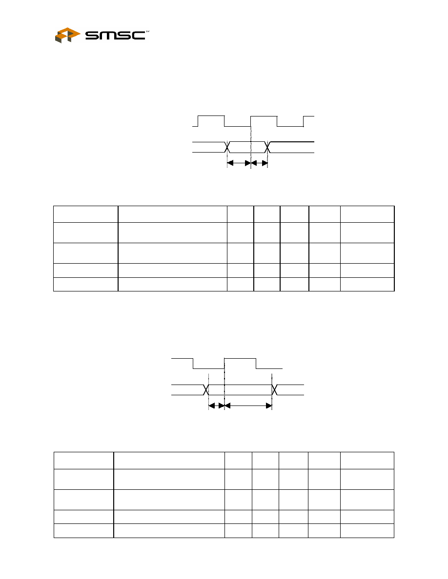
High Performance Single Chip Low Power 10/100 Ethernet Physical Layer Transceiver (PHY)
Datasheet
Rev. 0.8 (11-16-04)
52
SMSC LAN83C185
DATASHEET
6.2
100Base-TX Timings
6.2.1
100M MII Receive Timing
6.2.2
100M MII Transmit Timing
PARAMETER
DESCRIPTION
MIN
TYP
MAX
UNITS
NOTES
T2.1
Receive signals setup to RX_CLK
rising
10
ns
T2.2
Receive signals hold from
RX_CLK rising
10
ns
RX_CLK frequency
25
MHz
RX_CLK Duty-Cycle
40
%
PARAMETER
DESCRIPTION
MIN
TYP
MAX
UNITS
NOTES
T3.1
Transmit signals setup to TX_CLK
rising
12
ns
T3.2
Transmit signals hold after
TX_CLK rising
0
ns
TX_CLK frequency
25
MHz
TX_CLK Duty-Cycle
40
%
RX_CLK
RXD[3:0]
RX_DV
RX_ER
T2.1
Valid Data
T2.2
TX_CLK
TXD[3:0]
TX_EN
TX_ER
T3.1 T3.2
Valid Data
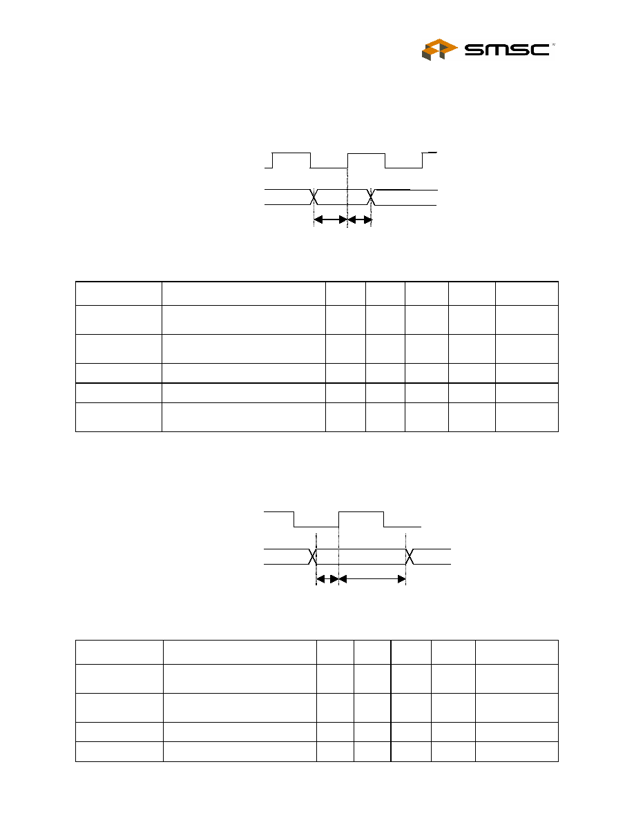
High Performance Single Chip Low Power 10/100 Ethernet Physical Layer Transceiver (PHY)
Datasheet
SMSC LAN83C185
53
Rev. 0.8 (11-16-04)
DATASHEET
6.3
10Base-T Timings
6.3.1
10M MII Receive Timing
6.3.2
10M MII Transmit Timing
PARAMETER
DESCRIPTION
MIN
TYP
MAX
UNITS
NOTES
T4.1
Receive signals setup to RX_CLK
rising
10
ns
T4.2
Receive signals hold from RX_CLK
rising
10
ns
RX_CLK frequency
25
MHz
RX_CLK Duty-Cycle
40
%
Receive signals setup to RX_CLK
rising
10
ns
PARAMETER
DESCRIPTION
MIN
TYP
MAX
UNITS
NOTES
T5.1
Transmit signals setup to
TX_CLK rising
12
ns
T5.2
Transmit signals hold after
TX_CLK rising
0
ns
TX_CLK frequency
2.5
MHz
TX_CLK Duty-Cycle
50
%
Valid Data
T4.1
T4.2
RX_CLK
RXD[3:0]
RX_DV
RX_ER
TX_CLK
TXD[3:0]
TX_EN
T5.1
T5.2
Valid Data
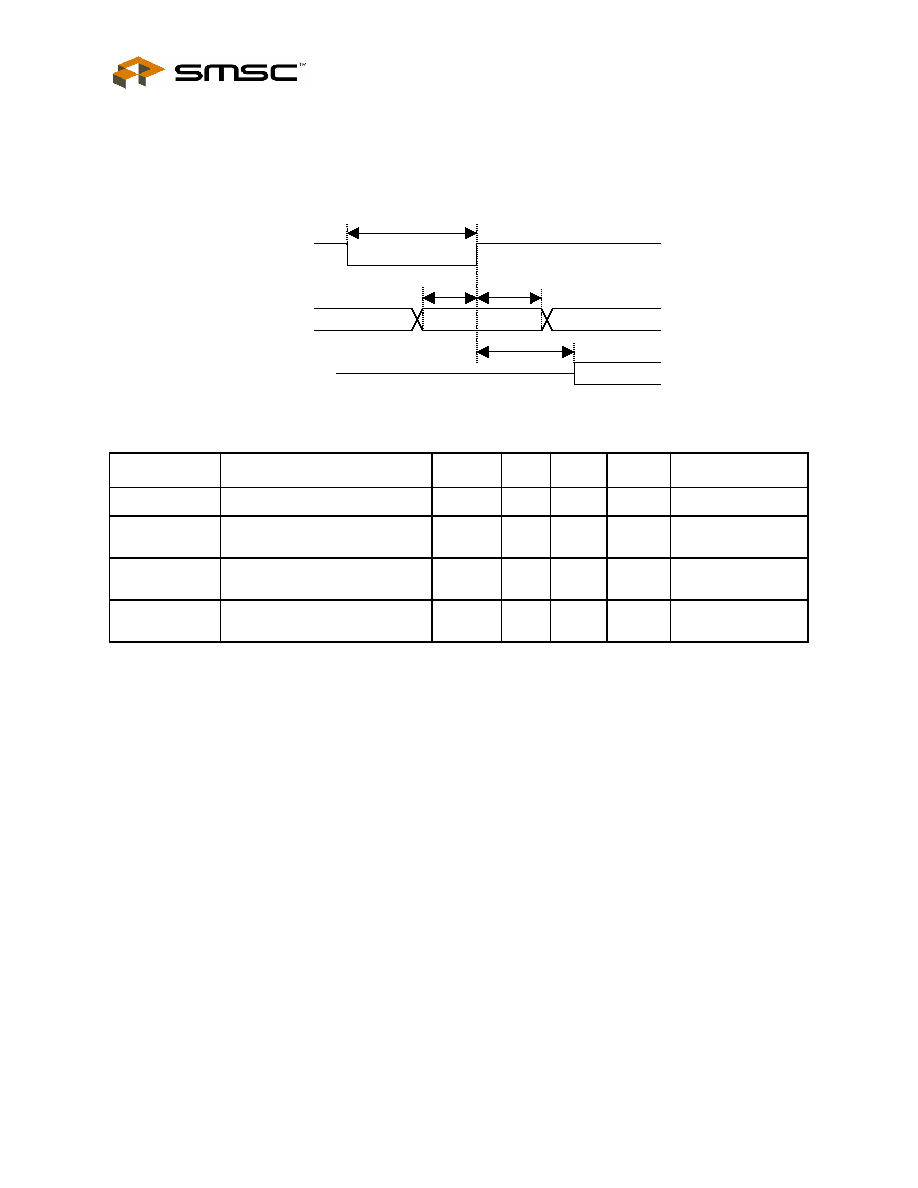
High Performance Single Chip Low Power 10/100 Ethernet Physical Layer Transceiver (PHY)
Datasheet
Rev. 0.8 (11-16-04)
54
SMSC LAN83C185
DATASHEET
6.4
Reset Timing
PARAMETER
DESCRIPTION
MIN
TYP
MAX
UNITS
NOTES
T6.1
Reset Pulse Width
100
us
T6.2
Configuration input setup to
nRST rising
200
ns
T6.3
Configuration input hold after
nRST rising
400
ns
T6.4
Output Drive after nRST rising
20
800
ns
20 clock cycles for
25 MHz clock
T6.1
T6.2
T6.3
nRST
Configuration
signals
Output drive
T6.4
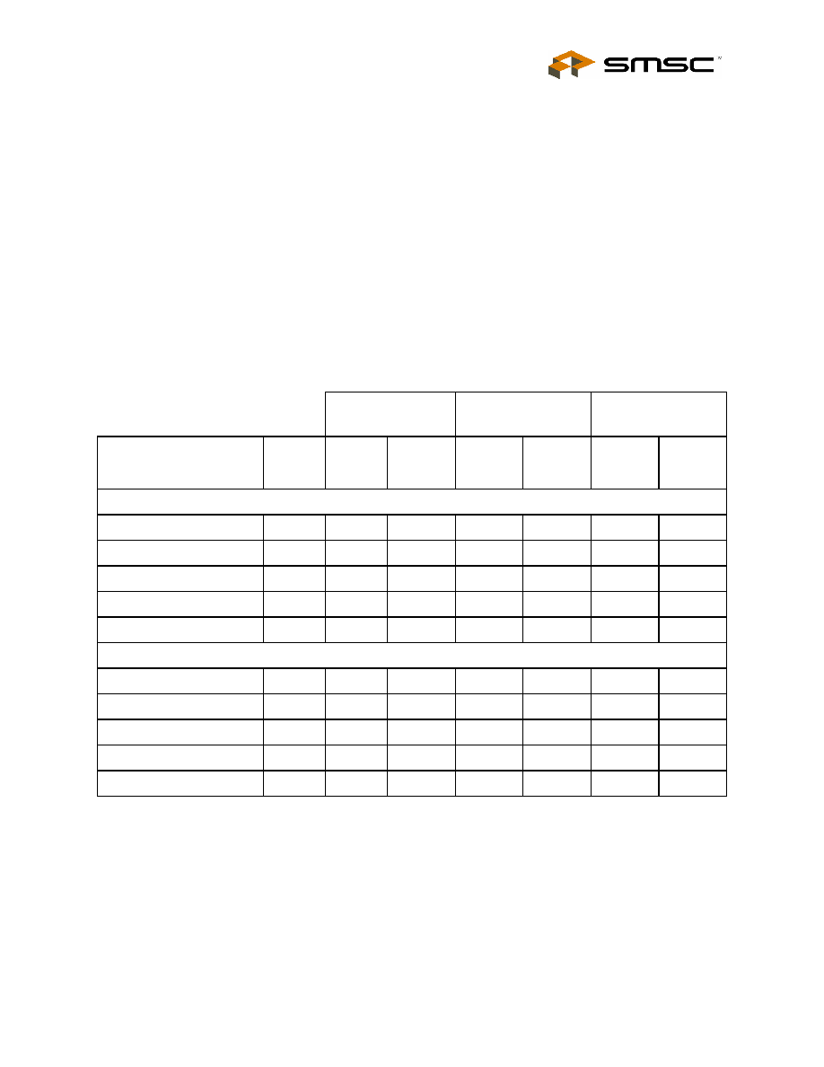
High Performance Single Chip Low Power 10/100 Ethernet Physical Layer Transceiver (PHY)
Datasheet
SMSC LAN83C185
55
Rev. 0.8 (11-16-04)
DATASHEET
6.5
DC Characteristics
6.5.1
Operating Conditions
Supply Voltage
+3.3V +/- 10%
Operating Temperature
0�C to 70�C
6.5.2
Power Consumption
6.5.2.1
Power Consumption Device Only
Power measurements taken under the following conditions:
Temperature:
+25
� C
Device VDD:
+3.30 V
Notes:
1. Each LED indicator in use adds approximately 4 mA to the Digital power supply.
2. Digital Power pins on LAN83C185 are: VDD pins 8, 18, 43.
3. Analog Power pins on LAN83C185 are: AVDD pins 53, 57, 61, 63.
4. Regulator Supply pins on LAN83C185 are: VREG pin 13.
5. Traffic Utilization = 100%
6. Mode of Operation in both cases is full duplex.
Table 6.1 Power Consumption Device Only
DIGITAL POWER
ANALOG POWER
REGULATOR
SUPPLY CURRENT
Mode
Total
Power
(mW)
Power
(mW)
Current
(mA)
Power
(mW)
Current
(mA)
Power
(mW)
Current
(mA)
10BASE-T Operation
10BASE-T /w traffic
96
33
10
59
18
4
1
Idle
83
20
6
59
18
4
1
Energy Detect Power Down
45
17
5
24
7
4
1
AN General Power Down
45
17
5
24
7
4
1
Non-AN Gen Power Down
22
17
5
0.66
0.200
4
1
100BASE-TX Operation
100BASE-TX /w traffic
261
66
20
132
40
63
19
Idle
245
50
15
132
40
63
19
Energy Detect Power Down
45
17
5
24
7
4
1
AN General Power Down
45
17
5
24
7
4
1
Non-AN Gen Power Down
22
17
5
0.66
0.200
4
1
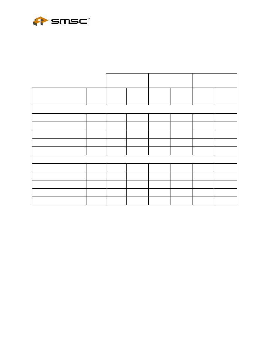
High Performance Single Chip Low Power 10/100 Ethernet Physical Layer Transceiver (PHY)
Datasheet
Rev. 0.8 (11-16-04)
56
SMSC LAN83C185
DATASHEET
6.5.2.2
Power Consumption Device and System Components
Power measurements taken under the following conditions:
Temperature:
+25
� C
Device VDD:
+3.30 V
Notes:
1. Each LED indicator in use adds approximately 4 mA to the Digital power supply.
2. Digital Power pins on LAN83C185 are: VDD pins 8, 18, 43.
3. Analog Power pins on LAN83C185 are: AVDD pins 53, 57, 61, 63.
4. Regulator Supply pins on LAN83C185 are: VREG pin 13.
5. Traffic Utilization = 100%
6. Mode of Operation in both cases is full duplex.
Table 6.2 Power Consumption Device and System Components
DIGITAL POWER
ANALOG POWER
REGULATOR
SUPPLY CURRENT
Mode
Total
Power
(mW)
Power
(mW)
Current
(mA)
Power
(mW)
Current
(mA)
Power
(mW)
Current
(mA)
10BASE-T Operation
10BASE-T /w traffic
476
33
10
439
133
4
1
Idle
463
20
6
439
133
4
1
Energy Detect Power Down
45
17
5
24
7
4
1
AN General Power Down
45
17
5
24
7
4
1
Non-AN Gen Power Down
22
17
5
.66
.200
4
1
100BASE-TX Operation
100BASE-TX /w traffic
400
66
20
271
82
63
19
Idle
384
50
15
271
82
63
19
Energy Detect Power Down
45
17
5
24
7
4
1
AN General Power Down
45
17
5
24
7
4
1
Non-AN Gen Power Down
22
17
5
.66
.200
4
1

High Performance Single Chip Low Power 10/100 Ethernet Physical Layer Transceiver (PHY)
Datasheet
SMSC LAN83C185
57
Rev. 0.8 (11-16-04)
DATASHEET
6.5.3
DC Characteristics - Input and Output Buffers
Table 6.3 MII BUS INTERFACE SIGNALS
PIN NO.
NAME
V
IH
V
IL
I
OH
I
OL
V
OL
V
OH
41
TXD0
+2.0 V
+0.8 V
42
TXD1
+2.0 V
+0.8 V
44
TXD2
+2.0 V
+0.8 V
45
TXD3
+2.0 V
+0.8 V
37
TX_ER/TXD4
+2.0 V
+0.8 V
39
TX_EN
+2.0 V
+0.8 V
38
TX_CLK
-8 mA
+8 mA
+0.4 V
VDD �
+0.4 V
32
RXD0
-8 mA
+8 mA
+0.4 V
VDD �
+0.4 V
31
RXD1
-8 mA
+8 mA
+0.4 V
VDD �
+0.4 V
30
RXD2
-8 mA
+8 mA
+0.4 V
VDD �
+0.4 V
29
RXD3
-8 mA
+8 mA
+0.4 V
VDD �
+0.4 V
35
RX_ER/RXD4
-8 mA
+8 mA
+0.4 V
VDD �
+0.4 V
33
RX_DV
-8 mA
+8 mA
+0.4 V
VDD �
+0.4 V
34
RX_CLK
-8 mA
+8 mA
+0.4 V
VDD �
+0.4 V
48
CRS
-8 mA
+8 mA
+0.4 V
VDD �
+0.4 V
47
COL
-8 mA
+8 mA
+0.4 V
VDD �
+0.4 V
27
MDC
+2.0 V
+0.8 V
26
MDIO
-8 mA
+8 mA
+0.4 V
VDD �
+0.4 V

High Performance Single Chip Low Power 10/100 Ethernet Physical Layer Transceiver (PHY)
Datasheet
Rev. 0.8 (11-16-04)
58
SMSC LAN83C185
DATASHEET
Table 6.4 LAN Interface Signals
PIN NO.
NAME
V
IH
V
IL
I
OH
I
OL
V
OL
V
OH
51
TXP
See
Table 6.10, "100Base-TX Transceiver Characteristics," on page 60
and
Table 6.11, "10BASE-T Transceiver Characteristics," on page 60
.
50
TXN
55
RXP
54
RXN
Table 6.5 LED Signals
PIN NO.
NAME
V
IH
V
IL
I
OH
I
OL
V
OL
V
OH
16
SPEED100
+2.0 V
+0.8 V
-12 mA
+24 mA
+0.4 V
VDD �
+0.4 V
17
LINKON
+2.0 V
+0.8 V
-12 mA
+24 mA
+0.4 V
VDD �
+0.4 V
19
ACTIVITY
+2.0 V
+0.8 V
-12 mA
+24 mA
+0.4 V
VDD �
+0.4 V
20
FDUPLEX
+2.0 V
+0.8 V
-12 mA
+24 mA
+0.4 V
VDD �
+0.4 V
Table 6.6 Configuration Inputs
PIN NO.
NAME
V
IH
V
IL
I
OH
I
OL
V
OL
V
OH
16
PHYAD0
+2.0 V
+0.8 V
-12 mA
+24 mA
+0.4 V
VDD �
+0.4 V
17
PHYAD1
+2.0 V
+0.8 V
-12 mA
+24 mA
+0.4 V
VDD �
+0.4 V
19
PHYAD2
+2.0 V
+0.8 V
-12 mA
+24 mA
+0.4 V
VDD �
+0.4 V
20
PHYAD3
+2.0 V
+0.8 V
-12 mA
+24 mA
+0.4 V
VDD �
+0.4 V
2
PHYAD4
-4 mA
+8 mA
+0.4 V
VDD �
+0.4 V
4
MODE0
+2.0 V
+0.8 V
5
MODE1
+2.0 V
+0.8 V
6
MODE2
+2.0 V
+0.8 V
9
TEST0
+2.0 V
+0.8 V
10
TEST1
+2.0 V
+0.8 V
11
CLK_FREQ
+2.0 V
+0.8 V
12
REG_EN

High Performance Single Chip Low Power 10/100 Ethernet Physical Layer Transceiver (PHY)
Datasheet
SMSC LAN83C185
59
Rev. 0.8 (11-16-04)
DATASHEET
1
MII
-4 mA
+8 mA
+0.4 V
VDD �
+0.4 V
Table 6.7 General Signals
PIN NO.
NAME
V
IH
V
IL
I
OH
I
OL
V
OL
V
OH
1
GPO0
-4 mA
+8 mA
+0.4 V
VDD �
+0.4 V
2
GPO1
-4 mA
+8 mA
+0.4 V
VDD �
+0.4 V
3
GPO2
-4 mA
+8 mA
+0.4 V
VDD �
+0.4 V
46
nINT
-4 mA
+8 mA
+0.4 V
VDD �
+0.4 V
25
nRST
23
CLKIN/XTAL1
22
XTAL2
64
NC1
Table 6.8 Analog References
PIN NO.
NAME
V
IH
V
IL
I
OH
I
OL
V
OL
V
OH
59
EXRES1
56
NC2
Table 6.9 Internal Pull-Up / Pull-/Down Configurations
PIN NO.
NAME
PULL-UP OR PULL-DOWN
TYPE
1
GPO0/MII
Pull-down
30 uA
2
GPO1/PHYAD4
Pull-up
30 uA
4
MODE0
Pull-up
30 uA
5
MODE1
Pull-up
30 uA
6
MODE2
Pull-up
30 uA
9
TEST0
Pull-down
30 uA
10
TEST1
Pull-down
30 uA
16
SPEED100
Pull-up
30 uA
Table 6.6 Configuration Inputs (continued)
PIN NO.
NAME
V
IH
V
IL
I
OH
I
OL
V
OL
V
OH
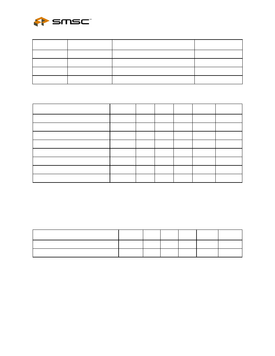
High Performance Single Chip Low Power 10/100 Ethernet Physical Layer Transceiver (PHY)
Datasheet
Rev. 0.8 (11-16-04)
60
SMSC LAN83C185
DATASHEET
Note 6.1
Measured at the line side of the transformer, line replaced by 100
(+/- 1%) resistor.
Note 6.2
Offset from16 nS pulse width at 50% of pulse peak
Note 6.3
Measured differentially.
Note 6.4
Min/max voltages guaranteed as measured with 100
resistive load.
17
LINKON
Pull-up
30 uA
19
ACTIVITY
Pull-up
30 uA
20
FDUPLEX
Pull-up
30 uA
46 nINT
Pull-up
30
uA
Table 6.10 100Base-TX Transceiver Characteristics
PARAMETER
SYMBOL
MIN
TYP
MAX
UNITS
NOTES
Peak Differential Output Voltage High
V
PPH
950
-
1050
mVpk
Note 6.1
Peak Differential Output Voltage Low
V
PPL
-950
-
-1050
mVpk
Note 6.1
Signal Amplitude Symmetry
V
SS
98
-
102
%
Note 6.1
Signal Rise & Fall Time
T
RF
3.0
-
5.0
nS
Note 6.1
Rise & Fall Time Symmetry
T
RFS
-
-
0.5
nS
Note 6.1
Duty Cycle Distortion
D
CD
35
50
65
%
Note 6.2
Overshoot & Undershoot
V
OS
-
-
5
%
Jitter
1.4
nS
Note 6.3
Table 6.11 10BASE-T Transceiver Characteristics
PARAMETER
SYMBOL
MIN
TYP
MAX
UNITS
NOTES
Transmitter Peak Differential Output Voltage
V
OUT
2.2
2.5
2.8
V
Note 6.4
Receiver Differential Squelch Threshold
V
DS
300
420
585
mV
Table 6.9 Internal Pull-Up / Pull-/Down Configurations (continued)
PIN NO.
NAME
PULL-UP OR PULL-DOWN
TYPE

High Performance Single Chip Low Power 10/100 Ethernet Physical Layer Transceiver (PHY)
Datasheet
SMSC LAN83C185
61
Rev. 0.8 (11-16-04)
DATASHEET
Chapter 7 Package Outline
Figure 7.1 64 Pin TQFP Package Outline, 10X10X1.4 Body, 2 MM Footprint
Notes:
1. Controlling Unit: millimeter.
2. Tolerance on the true position of the leads is � 0.04 mm maximum.
3. Package body dimensions D1 and E1 do not include the mold protrusion.
Maximum mold protrusion is 0.25 mm per side.
4. Dimension for foot length L measured at the gauge plane 0.25 mm above the seating plane.
5. Details of pin 1 identifier are optional but must be located within the zone indicated.
Table 7.1 64 Pin TQFP Package Parameters
MIN
NOMINAL
MAX
REMARKS
A
~
~
1.60
Overall Package Height
A1
0.05
~
0.15
Standoff
A2
1.35
~
1.45
Body Thickness
D
11.80
~
12.20
X Span
D1
9.80
~
10.20
X body Size
E
11.80
~
12.20
Y Span
E1
9.80
~
10.20
Y body Size
H
0.09
~
0.20
Lead Frame Thickness
L
0.45
0.60
0.75
Lead Foot Length
L1
~
1.00
~
Lead Length
e
0.50 Basic
Lead Pitch
0
o
~
7
o
Lead Foot Angle
W
0.17
0.22
0.27
Lead Width
R
0.08
~
~
Lead Shoulder Radius
R2
0.08
~
0.20
Lead Foot Radius
ccc
~
~
0.08
Coplanarity