 | –≠–ª–µ–∫—Ç—Ä–æ–Ω–Ω—ã–π –∫–æ–º–ø–æ–Ω–µ–Ω—Ç: LAN91C96 | –°–∫–∞—á–∞—Ç—å:  PDF PDF  ZIP ZIP |

SMSC LAN91C965v&3v
Page 1
Rev. 09/10/2004
DATASHEET
LAN91C96
Non-PCI Single-Chip
Full Duplex Ethernet
Controller with Magic
Packet
Datasheet
Product Features
Non-PCI Single-Chip Ethernet Controller
A Subset of Motorola 68000 Bus Interface
Support
Fully Supports Full Duplex Switched Ethernet
Supports Enhanced Transmit Queue
Management
6K Bytes of On-Chip RAM
Supports IEEE 802.3 (ANSI 8802-3) Ethernet
Standards
Automatic Detection of TX/RX Polarity Reversal
Enhanced Power Management Features
Supports "Magic Packet" Power Management
Technology
Simultasking Early Transmit and Early Receive
Functions
Enhanced Early Transmit Function
Receive Counter for Enhanced Early Receive
Hardware Memory Management Unit
Optional
Configuration via Serial EEPROM
Interface (Jumperless)
Supports single +5V or +3.3V (for Revisions E
and Later) VCC Designs
Supports Mixed Voltage External PHY Designs
1
Low Power CMOS Design
100 Pin QFP and TQFP (1.0 mm body
Thickness) Packages
Pin Compatible with the LAN91C92 and
LAN91C94
Bus Interface
Direct Interface to Local Bus, PCMCIA, and
68000 Buses with No Wait States
Flexible Bus Interface
16 Bit Data and Control Paths
Fast Access Time
1
Refer to Description of Pin Functions on Page 16 for
5V tolerant pins
Pipelined Data Path
Handles Block Word Transfers for any
Alignment
High Performance Chained ("Back-to-Back")
Transmit and Receive
Pin Compatible with the LAN91C92 (in Local
Bus Mode) and the LAN91C94 in Both Local
Bus and PCMCIA Modes
Dynamic Memory Allocation Between Transmit
and Receive
Flat Memory Structure for Low CPU Overhead
Buffered Architecture, Insensitive to Bus
Latencies (No Overruns/Underruns)
Supports Boot PROM for Diskless Local Bus
Applications
Network Interface
Integrated
10BASE-T
Transceiver
Functions:
-
Driver and Receiver
-
Link Integrity Test
-
Receive Polarity Detection and Correction
Integrated AUI Interface
10 Mb/s Manchester Encoding/Decoding and
Clock Recovery
Automatic Retransmission, Bad Packet
Rejection, and Transmit Padding
External and Internal Loopback Modes
Four Direct Driven LEDs for Status/ Diagnostics
Software Drivers
LAN9000 Drivers for Major Network Operating
Systems Utilizing Local Bus or PCMCIA
Interface
Software Drivers Compatible with the
LAN91C92, LAN91C94, LAN91C100FD (100
Mb/s), and LAN91C110 (100 Mb/s) Controllers
in Local Bus Mode
Software Drivers Utilize Full Capability of 32 Bit
Microprocessor

Non-PCI Single-Chip Full Duplex Ethernet Controller with Magic Packet
Rev. 09/10/2004
Page 2
SMSC LAN91C965v&3v
DATASHEET
ORDERING INFORMATION
Order Numbers:
LAN91C96 QFP for 100 Pin QFP Package
LAN91C96 TQFP for 100 Pin TQFP Package
LAN91C96-MS for 100 pin Lead Free QFP Package
LAN91C96-MU for 100 pin Lead Free TQFP Package
80 Arkay Drive
Hauppauge,
NY
11788
(631)
435-6000
FAX (631) 273-3123
Copyright © SMSC 2004. All rights reserved.
Circuit diagrams and other information relating to SMSC products are included as a means of illustrating typical applications. Consequently, complete
information sufficient for construction purposes is not necessarily given. Although the information has been checked and is believed to be accurate, no
responsibility is assumed for inaccuracies. SMSC reserves the right to make changes to specifications and product descriptions at any time without
notice. Contact your local SMSC sales office to obtain the latest specifications before placing your product order. The provision of this information does
not convey to the purchaser of the described semiconductor devices any licenses under any patent rights or other intellectual property rights of SMSC
or others. All sales are expressly conditional on your agreement to the terms and conditions of the most recently dated version of SMSC's standard
Terms of Sale Agreement dated before the date of your order (the "Terms of Sale Agreement"). The product may contain design defects or errors
known as anomalies which may cause the product's functions to deviate from published specifications. Anomaly sheets are available upon request.
SMSC products are not designed, intended, authorized or warranted for use in any life support or other application where product failure could cause
or contribute to personal injury or severe property damage. Any and all such uses without prior written approval of an Officer of SMSC and further
testing and/or modification will be fully at the risk of the customer. Copies of this document or other SMSC literature, as well as the Terms of Sale
Agreement, may be obtained by visiting SMSC's website at http://www.smsc.com. SMSC is a registered trademark of Standard Microsystems
Corporation ("SMSC"). Product names and company names are the trademarks of their respective holders.
SMSC DISCLAIMS AND EXCLUDES ANY AND ALL WARRANTIES, INCLUDING WITHOUT LIMITATION ANY AND ALL IMPLIED WARRANTIES
OF MERCHANTABILITY, FITNESS FOR A PARTICULAR PURPOSE, TITLE, AND AGAINST INFRINGEMENT AND THE LIKE, AND ANY AND
ALL WARRANTIES ARISING FROM ANY COURSE OF DEALING OR USAGE OF TRADE.
IN NO EVENT SHALL SMSC BE LIABLE FOR ANY DIRECT, INCIDENTAL, INDIRECT, SPECIAL, PUNITIVE, OR CONSEQUENTIAL DAMAGES;
OR FOR LOST DATA, PROFITS, SAVINGS OR REVENUES OF ANY KIND; REGARDLESS OF THE FORM OF ACTION, WHETHER BASED ON
CONTRACT; TORT; NEGLIGENCE OF SMSC OR OTHERS; STRICT LIABILITY; BREACH OF WARRANTY; OR OTHERWISE; WHETHER OR
NOT ANY REMEDY OF BUYER IS HELD TO HAVE FAILED OF ITS ESSENTIAL PURPOSE, AND WHETHER OR NOT SMSC HAS BEEN
ADVISED OF THE POSSIBILITY OF SUCH DAMAGES.

Non-PCI Single-Chip Full Duplex Ethernet Controller with Magic Packet
SMSC LAN91C965v&3v
Page 3
Rev. 09/10/2004
DATASHEET
TABLE OF CONTENTS
Chapter 1
General Description _________________________________________________________________________ 6
Chapter 2
Overview __________________________________________________________________________________ 7
Chapter 3
Pin Configurations_________________________________________________________________________ 10
3.1
Local Bus vs. PCMCIA vs. 68000 Pin Requirements ________________________________________________ 14
Chapter 4
Description of Pin Functions ________________________________________________________________ 16
4.1
Buffer Symbols _______________________________________________________________________________ 20
Chapter 5
Functional Description _____________________________________________________________________ 22
5.1
Buffer Memory _______________________________________________________________________________ 23
5.2
Interrupt Structure____________________________________________________________________________ 30
5.3
Reset Logic___________________________________________________________________________________ 31
5.4
Power Down Logic States_______________________________________________________________________ 31
5.5
LAN91C96 Power Down States __________________________________________________________________ 32
5.6
PCMCIA CONFIGURATION REGISTERS DESCRIPTION ________________________________________ 35
Chapter 6
Frame Format in Buffer Memory for Ethernet __________________________________________________ 37
Chapter 7
Registers Map in I/O Space __________________________________________________________________ 41
7.1
I/O Space Access ______________________________________________________________________________ 41
7.2
I/O Space Registers Description _________________________________________________________________ 41
Chapter 8
Theory of Operation________________________________________________________________________ 65
8.1
Typical Flow of Events for Transmit (Auto Release = 0) _____________________________________________ 67
8.2
Typical Flow of Events for Transmit (Auto Release = 1) _____________________________________________ 68
8.3
Flow of Events for Receive ______________________________________________________________________ 69
Chapter 9
Functional Description of the Blocks __________________________________________________________ 79
9.1
Memory Management Unit _____________________________________________________________________ 79
9.2
Arbiter ______________________________________________________________________________________ 79
9.3
Bus Interface _________________________________________________________________________________ 80
9.4
Wait State Policy ______________________________________________________________________________ 80
9.5
Arbitration Considerations _____________________________________________________________________ 81
9.6
DMA Block __________________________________________________________________________________ 81
9.7
Packet Number FIFOS_________________________________________________________________________ 82
9.8
CSMA Block _________________________________________________________________________________ 84
9.9
Network Interface _____________________________________________________________________________ 85
9.10
10Base-T___________________________________________________________________________________ 86
9.11
AUI _______________________________________________________________________________________ 86
9.12
Physical Interface ___________________________________________________________________________ 86
9.13
Transmit Functions__________________________________________________________________________ 86
9.13.1
Manchester Encoding _______________________________________________________________________ 86
9.13.2
Transmit Drivers ___________________________________________________________________________ 87
9.13.3
Jabber Function____________________________________________________________________________ 87

Non-PCI Single-Chip Full Duplex Ethernet Controller with Magic Packet
Rev. 09/10/2004
Page 4
SMSC LAN91C965v&3v
DATASHEET
9.13.4
SQE Function _____________________________________________________________________________ 87
9.14
Receive Functions ___________________________________________________________________________ 87
9.14.1
Receive Drivers____________________________________________________________________________ 87
9.14.2
Manchester Decoder and Clock Recovery _______________________________________________________ 87
9.14.3
Squelch Function __________________________________________________________________________ 87
9.14.4
Reverse Polarity Function____________________________________________________________________ 88
9.14.5
Collision Detection Function _________________________________________________________________ 88
9.14.6
Link Integrity _____________________________________________________________________________ 88
Chapter 10
Board Setup Information____________________________________________________________________ 89
10.1
Diagnostic LEDs ____________________________________________________________________________ 90
10.2
Bus Clock Considerations ____________________________________________________________________ 90
10.3
68000 Bus Interface__________________________________________________________________________ 90
Chapter 11
Operational Description_____________________________________________________________________ 92
11.1
Maximum Guaranteed Ratings* _______________________________________________________________ 92
11.2
DC Electrical Characteristics _________________________________________________________________ 92
Chapter 12
Timing Diagrams __________________________________________________________________________ 99
Chapter 13
LAN91C96 Revisions ______________________________________________________________________ 125
LIST OF FIGURES
Figure 3.1 - LAN91C96 100 Pin QFP...........................................................................................................................10
Figure 3.2 - LAN91C96 100 Pin TQFP.........................................................................................................................11
Figure 3.3 - LAN91C96 System Block Diagram ...........................................................................................................12
Figure 3.4 ≠ System Diagram for Local Bus with Boot Prom .......................................................................................13
Figure 4.1 - LAN91C96 Internal Block Diagram ...........................................................................................................21
Figure 5.1 ≠ Mapping and Paging vs. Receive and Transmit Area ..............................................................................24
Figure 5.2 ≠ Transmit Queues and Mapping................................................................................................................25
Figure 5.3 ≠ Receive Queues and Mapping.................................................................................................................26
Figure 5.4 - LAN91C96 Internal Block Diagram with Data Path...................................................................................27
Figure 5.5 ≠ Logical Address Generation and Relevant Registers...............................................................................28
Figure 6.1 ≠ Data Frame Format..................................................................................................................................37
Figure 6.2 - LAN91C96 Registers ................................................................................................................................40
Figure 7.1 ≠ Interrupt Structure.....................................................................................................................................61
Figure 8.1 ≠ Interrupt Service Routine .........................................................................................................................70
Figure 8.2 - RX INTR ...................................................................................................................................................71
Figure 8.3 -TX INTR.....................................................................................................................................................72
Figure 8.4 -TXEMPTY INTR ........................................................................................................................................73
Figure 8.5 ≠ Driver Send and Allocate Routines ..........................................................................................................74
Figure 8.6 ≠ Interrupt Generation for Transmit; Receive, MMU ...................................................................................78
FIGURE 9.1 - MMU PACKET NUMBER FLOW AND RELEVANT REGISTERS.........................................................84
FIGURE 10.1 - 64 X 16 SERIAL EEPROM MAP .........................................................................................................91
Figure 12.1 ≠ Card Configuration Registers ≠ Read/Write PCMCIA Mode (A15=1) ....................................................99
Figure 12.2 ≠ Local Bus Consecutive Read Cycles ...................................................................................................100
Figure 12.3 - PCMCIA Consecutive Read Cycles ......................................................................................................101
Figure 12.4 ≠ Local Bus Consecutive Write Cycles....................................................................................................102
Figure 12.5 - PCMCIA Consecutive Write Cycles ......................................................................................................103
Figure 12.6 ≠ Local Bus Consecutive Read and Write Cycles ...................................................................................104
Figure 12.7 ≠ Data Register Special Read Access ....................................................................................................105
Figure 12.8 ≠ Data Register Special Write Access.....................................................................................................106
Figure 12.9 - 8-Bit Mode Register Cycles ..................................................................................................................107
Figure 12.10 - 68000 Read Timing.............................................................................................................................108
Figure 12.11 - 68000 Write Timing.............................................................................................................................109
Figure 12.12 ≠ External ROM Read Access ..............................................................................................................110
Figure 12.13 ≠ Local Bus Register Access When Using Bale....................................................................................111

Non-PCI Single-Chip Full Duplex Ethernet Controller with Magic Packet
SMSC LAN91C965v&3v
Page 5
Rev. 09/10/2004
DATASHEET
Figure 12.14 ≠ External ROM Read Access Using Bale ............................................................................................112
Figure 12.15 - EEPROM Read...................................................................................................................................113
Figure 12.16 - EEPROM Write ...................................................................................................................................114
Figure 12.17 - PCMCIA Attribute Memory Read/Write (A15=0) .................................................................................115
Figure 12.18 ≠ External ENDEC Interface ≠ Start of Transmit ...................................................................................115
Figure 12.19 ≠ External ENDEC Interface ≠ Receive Data ........................................................................................116
Figure 12.20 ≠ Differential Output Signal Timing (10BASE-T and AUI) .....................................................................117
Figure 12.21 ≠ Receive Timing ≠ Start of Frame (AUI and 10BASE-T) .....................................................................118
Figure 12.22 ≠ Receive Timing ≠ End of Frame (AUI and 10BASE-T).......................................................................119
Figure 12.23 ≠ Transmit Timing ≠ End of Frame (AUI and 10BASE-T)......................................................................120
Figure 12.24 ≠ Collision Timing (AUI) ........................................................................................................................121
Figure 12.25 ≠ Memory Read Timing.........................................................................................................................121
Figure 12.26 ≠ Input Clock Timing .............................................................................................................................122
Figure 12.27 ≠ Memory Write Timing .........................................................................................................................122
Figure 12.28 - 100 PIN QFP Package........................................................................................................................123
Figure 12.29 - 100 PIN TQFP Package .....................................................................................................................124
LIST OF TABLES
Table 5.1 - LAN91C96 Address Space ........................................................................................................................29
Table 5.2 - Bus Transactions In LOCAL BUS Mode ....................................................................................................29
Table 5.3 - Bus Transactions In PCMCIA Mode...........................................................................................................30
Table 5.4 - Bus Transactions In 68000 Mode................................................................................................................30
Table 5.5 - Interrupt Merging........................................................................................................................................31
Table 5.6 - LOCAL BUS Mode Defined States (Refer To Table 5.7 For Next States To Wake-Up Events).................32
Table 5.7- LOCAL BUS Mode......................................................................................................................................32
Table 5.8 - PCMCIA Mode (Refer To Table 5.7 For Next States To Wake-Up Events) ...............................................33
Table 5.9 - PCMCIA Mode ...........................................................................................................................................33
Table 7.1 - Transmit Loop ............................................................................................................................................44

Non-PCI Single-Chip Full Duplex Ethernet Controller with Magic Packet
Rev. 09/10/2004
Page 6
SMSC LAN91C965v&3v
DATASHEET
Chapter 1 General Description
The LAN91C96 is a VLSI Ethernet Controller that combines Local Bus, PCMCIA, and Motorola 68000 bus
interfaces in one chip. LAN91C96 integrates all MAC and physical layer functions, as well as the packet
RAM, needed to implement a high performance 10BASE-T (twisted pair) node. For 10BASE5 (thick coax),
10BASE2 (thin coax), and 10BASE-F (fiber) implementations, the LAN91C96 interfaces to external
transceivers via the provided AUI port. Only one additional IC is required for most applications. The
LAN91C96 comes with Full Duplex Switched Ethernet (FDSWE) support allowing the controller to provide
much higher throughput. 6K bytes of RAM is provided to support enhanced throughput and compensate
for any increased system service latencies. The controller implements multiple advanced power-down
modes including Magic Packet to conserve power and operate more efficiently. The LAN91C96 can
directly interface with the Local Bus, PCMCIA, and 68000 buses and deliver no-wait-state operation. For
Local Bus and PCMCIA interfaces, the LAN91C96 occupies 16 I/0 locations and no memory space except
for PCMCIA attribute memory space. The same I/O space is used for both LOCAL BUS and PCMCIA
operations. Its shared memory is sequentially accessed with 40ns access times to any of its registers,
including its packet memory. DMA services are not used by the LAN91C96, virtually de-coupling network
traffic from local or system bus utilization. For packet memory management, the LAN91C96 integrates a
unique hardware Memory Management Unit (MMU) with enhanced performance and decreased software
overhead when compared to ring buffer and linked list architectures. The LAN91C96 is portable to
different CPU and bus platforms due to its flexible bus interface, flat memory structure (no pointers), and
its loosely coupled buffered architecture (not sensitive to latency).
The LAN91C96 is available in 100-pin QFP and TQFP (1.0 mm body thickness) packages. The low profile
TQFP is ideal for mobile applications such as PC Card LAN adapters. The LAN91C96 operates with a
single power supply voltage of 5.0V. Revisions E and later will also operate using a single 3.3V power
supply.

Non-PCI Single-Chip Full Duplex Ethernet Controller with Magic Packet
SMSC LAN91C965v&3v
Page 7
Rev. 09/10/2004
DATASHEET
Chapter 2 Overview
A unique architecture allows the LAN91C96 to combine high performance, flexibility, high integration and
simple software interface.
The LAN91C96 incorporates the LAN91C92 functionality for LOCAL BUS environments, as well as a
PCMCIA interface and attribute registers like the LAN91C94 It also includes a subset of the Motorola
68000 interface. Mode selection between LOCAL BUS and PCMCIA is static and is done only at the end
of a reset. Selection of 68000 operation mode is performed at power-up.
The LAN91C96 consists of the same logical I/O register structure in LOCAL BUS and PCMCIA modes.
However, some of the signals used to access the PCMCIA differ from the LOCAL BUS mode. The MMU
(Memory Management Unit) architecture used by the LAN91C96 combines the simplicity and low
overhead of fixed areas with the flexibility of linked lists providing improved performance over other
methods.
Packet reception and transmission are determined by memory availability. All other resources are always
available if memory is available. To complement this flexible architecture, bus interface functions are
incorporated in the LAN91C96, as well as a 6144 byte packet RAM - and serial EEPROM-based setup.
The user can select or modify configuration choices. The LAN91C96 integrates most of the 802.3
functionality, incorporating the MAC layer protocol, the physical layer encoding and decoding functions
with the ability to handle the AUI interface. For twisted pair networks, LAN91C96 integrates the twisted pair
transceiver as well as the link integrity test functions.
The LAN91C96 is a true 10BASE-T single chip device able to interface to a system or a local bus.
Support for direct-driven LEDs for installation and run-time diagnostics is provided. 802.3 statistics are
gathered to facilitate network management.
The LAN91C96 is a single chip Ethernet controller designed to be 100% pin and software compatible with the
LAN91C92 and LAN91C94 in LOCAL BUS mode. Similar to the LAN91C94, the LAN91C96 has support
necessary for providing a true single chip single function PCMCIA Ethernet socket adapter. The LAN91C96
incorporates all of the PCMCIA registers and signals that interface to the PCMCIA bus.
The LAN91C96 has been designed to support full duplex switched Ethernet and provides Fully independent
transmit and receive operations.
The LAN91C96 internal packet memory is extended to 6k bytes, and the MMU will continue to manage
memory in 256 byte pages. The increase in memory size accommodates the potential for simultaneous
transmit and receive traffic in some full duplex applications as well as support for enhanced performance on
systems that introduce increased latency.
The LAN91C96 has the ability to retrieve configuration information from a serial EEPROM on reset or power-
up. In LOCAL BUS mode, the serial EPROM acts as storage of configuration and IEEE Ethernet address
information compatible with the existing LAN91C90, LAN91C92, and LAN91C94 LOCAL BUS Ethernet
controllers. In PCMCIA mode, the EEPROM function is the same as in LOCAL BUS mode. External Flash
ROM is required for CIS storage.
THE LAN91C96 OFFERS:
High integration:
Single chip controller including:
Packet
RAM
LOCAL BUS interface

Non-PCI Single-Chip Full Duplex Ethernet Controller with Magic Packet
Rev. 09/10/2004
Page 8
SMSC LAN91C965v&3v
DATASHEET
PCMCIA interface
68000 interface
EEPROM
interface
Encoder/decoder with AUI interface
10BASE-T
transceiver
High performance:
Chained ("Back-to-back") packet handling with no CPU intervention:
Queues transmit packets
Queues receive packets
Stores results in memory along with packet
Queues
interrupts
Optional single interrupt upon completion of transmit chain
Fast block move operation for load/unload:
CPU sees packet bytes as if stored continuously.
Handles 16 bit transfers regardless of address alignment.
Access to packet through fixed window.
Fast bus interface:
Compatible with LOCAL BUS type and faster buses.
Flexibility:
Flexible packet and header processing:
Can be set to Simultasking - Early Receive and Transmit modes. With enhanced Early Receive
functions.
Can access any byte in the packet.
Can immediately remove undesired packets from queue.
Can move packets from receive to transmit queue.
Can alter receive processing order without copying data.
Can discard or enqueue again a failed transmission.
Resource allocation:
Memory dynamically allocated for transmit and receive.
Can automatically release memory on successful transmission.
Configuration:
LOCAL BUS:
Uses non-volatile jumperless setup via serial EEPROM.
PCMCIA:
Uses ROM or Flash ROM for attribute memory storage and optional serial EEPROM for IEEE
address storage. PCMCIA I/O ignores address lines A4-A15 and relies on the PCMCIA host,
decoding for the slot.
nROM/nPCMCIA, on LAN91C96, is left open with a pullup for LOCAL BUS mode. This pin is
sampled at the end of RESET. If found low, the LAN91C96 is configured for PCMCIA mode.

Non-PCI Single-Chip Full Duplex Ethernet Controller with Magic Packet
SMSC LAN91C965v&3v
Page 9
Rev. 09/10/2004
DATASHEET
Motorola 68000:
Uses
non-volatile
jumperless
setup via serial EEPROM. The device must power up in LOCAL BUS
mode with nIORD and nIOWR asserted simultaneously to make the controller enter the 68000
mode.
Note:
The first write to the 68000 configured controller must be a write.

Non-PCI Single-Chip Full Duplex Ethernet Controller with Magic Packet
Rev. 09/10/2004
Page 10
SMSC LAN91C965v&3v
DATASHEET
Chapter 3 Pin Configurations
AVDD
COLN
COLP
RECN
RECP
TPERXN
TPERXP
AVSS
AVSS
RBIAS
AVDD
nXENDEC
nEN16
VSS
nROM/nPCMCIA
XTAL1
XTAL2
IOS0
IOS1
VDD
81
82
83
84
85
86
87
88
89
90
91
92
93
94
95
96
97
98
99
100
nIO
C
S
16/nIO
I
S
1
6
VSS
A2
A0
A1
BAL
E
/
n
W
E
n
SBH
E/n
C
E2
IN
TR3
IN
TR20
VDD
IN
TR1/nIN
P
A
C
K
D1
5
D1
4
D1
3
D1
2
VDD
D1
1
D1
0
D9
D8
VSS
EESK
EEDI
EEDO/SDO
U
T
ENEE
P
VSS
EECS
IO
S2
VSS
IN
TR0/nIR
E
Q
/IN
TR
1 2 3 4 5 6 7 8 9 10 1112 13 14 15 16 17 18 19 20 2122 23 24 25 26 2728 29 30
VDD
A19/nCE1
A18
A17
A16
A15
A14
A13
A12
A11/nFCS
VDD
A10/nFWE
A9
A8
A7
A6
A5
A4
A3
VSS
50
49
48
47
46
45
44
43
42
41
40
39
38
37
36
35
34
33
32
31
LAN91C96
100 Pin QFP
80 79 78 77 76 75 74 73 72 71 70 69 68 67 66 65 64 63 62 61 60 59 58 57 56 55 54 53 52 51
n
T
XL
ED/n
TX
EN
PW
RDW
N/
T
X
CL
K
n
I
ORD/
x
D
S
n
I
OW
R/
R/
n
W
nM
E
M
R
/
nOE
AEN/n
REG
/
n
A
S
I
O
CHRDY/
n
W
A
I
T
VS
S
D0
D1
D2
D3
VD
D
D4
D5
D6
D7
VS
S
RESE
T
BSEL
ED/R
XD
n
L
N
KL
ED/TX
D
n
R
XL
ED/RXC
L
K
AVD
D
TPETX
D
P
TPETX
D
N
TPET
XP
T
X
N/
n
C
RS
TXP/n
C
OL
L
AVS
S
TPETX
N
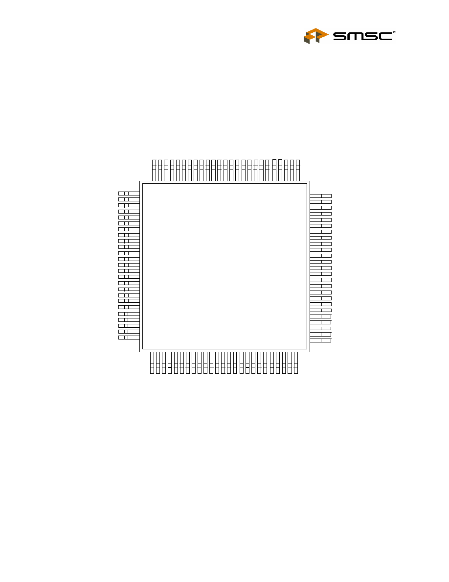
Figure 3.1 - LAN91C96 100 Pin QFP
Non-PCI Single-Chip Full Duplex Ethernet Controller with Magic Packet
SMSC LAN91C965v&3v
Page 11
Rev. 09/10/2004
DATASHEET
ENEEP
EEDO/SDOUT
EEDI
EECS
EESK
VSS
D8
D9
D10
D11
VDD
D12
D13
D14
D15
VSS
INTR0/nIREQ/INTR
INTR1/nINPACK
VDD
INTR2
INTR3
VSS
nIOCS16/nIOIS16
nSBHE/nCE2
BALE/nWE
1
2
3
4
5
6
7
8
9
10
11
12
13
14
15
16
17
18
19
20
21
22
23
24
25
A0
A1
A2
VSS
A3
A4
A5
A6
A7
A8
A9
A10
/
nFW
E
VDD
A11
/
nFCS
A12
A13
A14
A15
A16
A17
A18
A19
/
nCE1
VDD
nI
O
R
D
/
xD
S
n
I
O
W
R/
R/
n
W
26
27
28
29
30
31
32
33
34
35
36
37
38
39
40
41
42
43
44
45
46
47
48
49
50
TPETXP
TPETXDN
TPETXN
TPETXDP
AVDD
nTXLED/nTXEN
nRXLED/RXCLK
nLNKLED/TXD
nBSELED/RXD
PWRDWN/TXCLK
RESET
VSS
D7
D6
D5
D4
VDD
D3
D2
D1
D0
VSS
IOCHRDY/nWAIT
AEN/nREG/nAS
nMEMR/OE
75
74
73
72
71
70
69
68
67
66
65
64
63
62
61
60
59
58
57
56
55
54
53
52
51
VSS
IOS
2
VDD
IOS
1
IOS
0
XT
A
L
2
XT
A
L
1
n
R
OM/n
P
C
MC
IA
VSS
nEN
1
6
nXEN
DEC
AV
D
D
RB
I
A
S
A
VSS
A
VSS
TPE
R
XP
TPE
R
XN
RE
C
P
RE
C
N
CO
LP
CO
LN
AV
D
D
A
VSS
TXP/
nC
O
L
L
TXN/
n
CRS
100 99
98
97
96
95
94
93
92
91
90
89
88
87
86
85
84
83
82
81
80
79
78
77
76
LAN91C96
100 Pin TQFP
Figure 3.2 - LAN91C96 100 Pin TQFP
Non-PCI Single-Chip Full Duplex Ethernet Controller with Magic Packet
Rev. 09/10/2004
Page 12
SMSC LAN91C965v&3v
DATASHEET
Figure 3.3 - LAN91C96 System Block Diagram
SINGLE FUNCTION PCMCIA
CARD WITH THE LAN91C96
LAN91C96
nCE1, nCE2, nREG, nWE
nIREQ
D0-15
RESET
nIORD, nIOWR
A0-9, A15
nIOIS16, nINPACK
nWAIT
nCE
nWE
nOE
nOE
D0-7
A0-X
Attribute
Eprom
2816
PCMCIA CONNECTOR
10BASE-T / AUI
INTERFACE
STSCHG
nFWE
nFCS
Extended
CS,SK,DI,DO
Serial Eprom
(ISA-Hy9346)
(PCMCIA)
Non-PCI Single-Chip Full Duplex Ethernet Controller with Magic Packet
SMSC LAN91C965v&3v
Page 13
Rev. 09/10/2004
DATASHEET
T
P
E
T
X
P
T
P
E
T
X
N
T
P
E
T
X
D
P
T
P
E
T
X
D
N
T
P
E
R
X
P
T
P
E
R
X
N
T
X
P
T
X
N
R
E
C
P
R
E
C
N
C
OL
P
C
O
L
N
X
T
A
L
1
X
T
A
L
2
E
E
D
I
E
E
C
S
E
E
D
O
E
E
S
K
I
O
S
0
I
O
S
1
I
O
S
2
n
E
N
1
6
E
N
E
E
P
A
E
N
B
A
L
E
R
E
S
E
T
n
S
B
H
E
n
I
O
R
D
,
n
I
O
W
R
,
n
M
E
M
R
D
0
-
1
5
A
0
-
1
9
n
R
O
M
n
I
OC
S
1
6
I
OC
H
R
D
Y
I
N
T
R
0
-
3
CABLE SIDE
4
S
E
R
I
A
L
E
E
P
R
O
M
4
2
0
M
H
z
3
S
Y
S
T
E
M
B
U
S
A
D
D
R
E
S
S
P
R
O
M
D
A
T
A
n
I
R
Q
4
L
A
N
9
1
C
9
6
N
/
C
R
B
I
A
S
B
U
F
F
E
R
DIAGNOSTIC
LEDs
10BASET
AUI
Figure 3.4 ≠ System Diagram for Local Bus with Boot Prom

Non-PCI Single-Chip Full Duplex Ethernet Controller with Magic Packet
Rev. 09/10/2004
Page 14
SMSC LAN91C965v&3v
DATASHEET
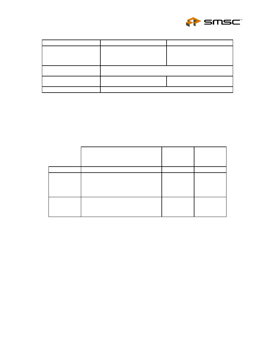
3.1
Local Bus vs. PCMCIA vs. 68000 Pin Requirements
FUNCTION LOCAL
BUS PCMCIA
68000
MAX
NUMBER OF
PINS
SYSTEM ADDRESS
BUS
A0
A1-9
A10
A11
A12-14
A15
A16-18
A19
AEN
A0
A1-9
nFWE
nFCS
A15
nCE1
nREG
A1-9
A10
A11
A12-14
A15
A16-18
A19
nAS
21
SYSTEM DATA BUS
D0-15
D0-15
D0-15
2
16
SYSTEM CONTROL
BUS
RESET
BALE
nIORD
nIOWR
nMEMR
IOCHRDY
nIOCS16
nSBHE
INTR0
INTR1
INTR2
INTR3
RESET
nWE
nIORD
nIOWR
nOE
nWAIT
nIOIS16
nCE2
nIREQ
nINPACK
RESET
xDS
R/nW
INTR
12
SERIAL EEPROM
EEDI
EEDO
EECS
EESK
ENEEP
IOS0
IOS1
IOS2
EEDI
EEDO
EECS
EESK
ENEEP
IOS0
IOS1
IOS2
EEDI
EEDO
EECS
EESK
ENEEP
IOS0
IOS1
IOS2
8
CRYSTAL OSC.
XTAL1, XTAL2
XTAL1, XTAL2
XTAL1, XTAL2
2
POWER
VDD, AVDD
VDD, AVDD
VDD, AVDD
9
GROUND GND,
AGND
GND, AGND
GND, AGND
11
10BASE-T interface
TPERXP
TPERXN
TPETXP
TPETXN
TPETXDP
TPETXDN
TPERXP
TPERXN
TPETXP
TPETXN
TPETXDP
TPETXDN
TPERXP
TPERXN
TPETXP
TPETXN
TPETXDP
TPETXDN
6
AUI interface
RECP RECN
COLP COLN
TXP/nCOLL
TXN/nCRS
RECP RECN
COLP COLN
TXP/nCOLL
TXN/nCRS
RECP RECN
COLP COLN
TXP/nCOLL
TXN/nCRS
6
2
The bytes connect to the 68000 host processor swapped

Non-PCI Single-Chip Full Duplex Ethernet Controller with Magic Packet
SMSC LAN91C965v&3v
Page 15
Rev. 09/10/2004
DATASHEET
FUNCTION LOCAL
BUS PCMCIA
68000
MAX
NUMBER OF
PINS
LEDs
nLNKLED/TXD
nRXLED/RXCLK
nBSELED/RXD
nTXLED/nTXEN
nLNKLED/TXD
nRXLED/RXCLK
nBSELED/RXD
nTXLED/nTXEN
nLNKLED/TXD
nRXLED/RXCLK
nBSELED/RXD
nTXLED/nTXEN
4
MISC. RBIAS
PWRDWN/TX
CLK
nXENDEC
nEN16
nROM
RBIAS
PWRDWN/TX
CLK
nXENDEC
nEN16
nPCMCIA
RBIAS
PWRDWN/TXC
LK nXENDEC
nEN16
nROM
5

Non-PCI Single-Chip Full Duplex Ethernet Controller with Magic Packet
Rev. 09/10/2004
Page 16
SMSC LAN91C965v&3v
DATASHEET
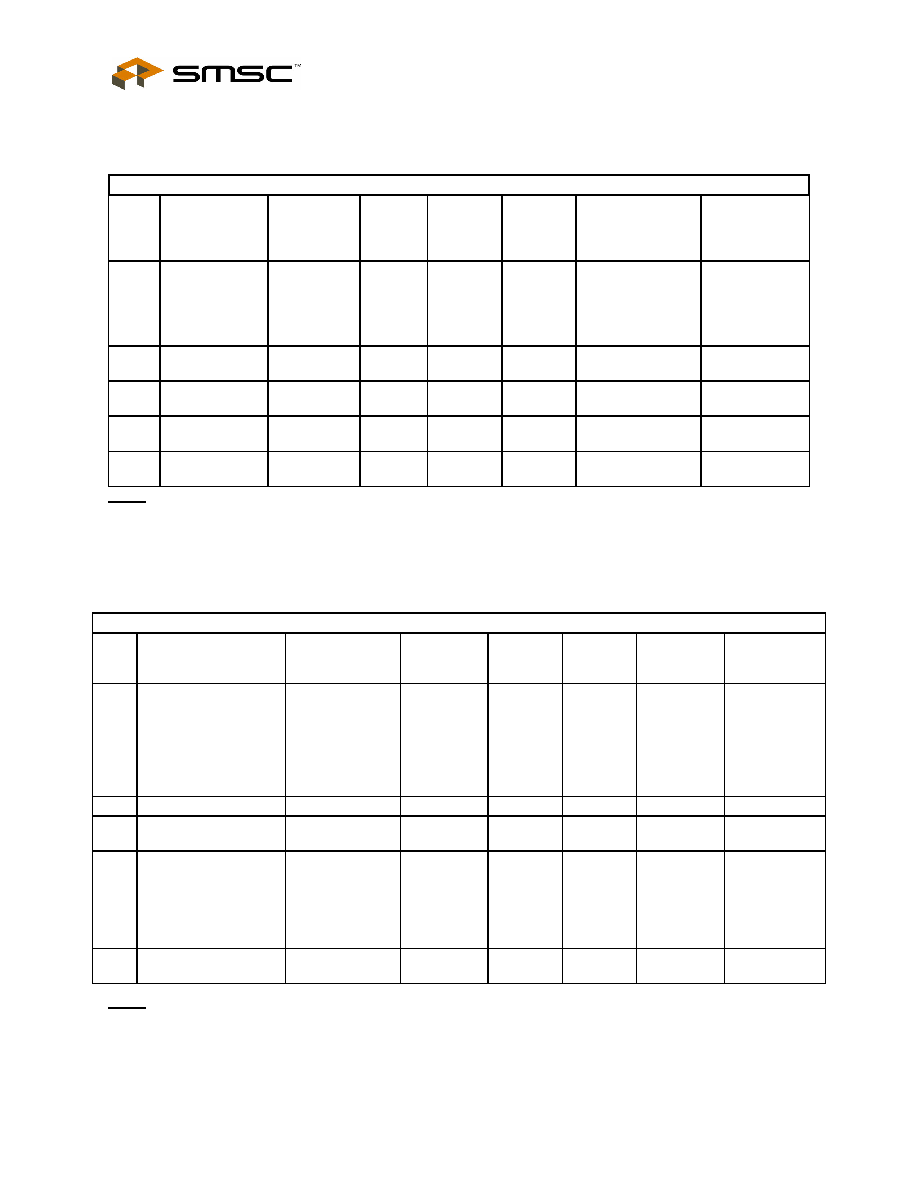
Chapter 4 Description of Pin Functions
PIN NO.
TQFP QFP PIN
NAME TYPE
DESCRIPTION
93 95
nROM/
nPCMCIA
I/O4 with
pullup
This pin is sampled at the end of RESET. When this
pin is sampled low the LAN91C96 is configured for
PCMCIA operation and all pin definitions correspond
to the PCMCIA mode. For LOCAL BUS operation this
pin is left open and it is used as a ROM chip select
output that goes active when nMEMR is low and the
address bus contains a valid ROM address. In
LOCAL BUS mode the LAN91C96 is pin compatible
with the LAN91C92 and LAN91C94. To enter the
68000 mode, this pin must be in the LOCAL BUS
mode at power up.
26-28
30-36
28,29,
30, 32-
38
A0-9 I
**
Input address lines 0 through 9.
37
39
A10/nFWE
I
LOCAL BUS - Input address line 10.
O4
PCMCIA - Output. Flash Memory Write Enable used
for programming the attribute memory. Goes active
(low) when WE*=0 and COR2=1.
39
41
A11/nFCS
I
LOCAL BUS - Input address line 11.
O4
PCMCIA - Output. Flash Memory Chip Select used to
access attribute memory. Goes active (low) when
nREG=0 nCE1=0 and A15=0.
40-46 42-48
A12-18
I
**
Input address lines 12 through 18.
47 49
A19/nCE1
I with
pullup
LOCAL BUS - Input address line 19.
**
PCMCIA - Card Enable 1 input. Used to select card on
even byte accesses.
52 54
AEN/
nREG/
nAS
I with
pullup
**
LOCAL BUS - Address enable input. Used as an
address qualifier. Address decoding is only enabled
when AEN is low.
PCMCIA - Attribute memory and IO select input.
Asserted when the card attribute space or IO space is
being accessed.
68000 ≠ Active low input. Address strobe.
24 26
nSBHE/
nCE2
I with
pullup
**
LOCAL BUS - Byte High Enable input. Asserted (low)
by the system to indicate a data transfer on the upper
data byte.
PCMCIA - Card Enable 2 input. Used to select card on
odd byte accesses.
53 55
IOCHRDY/
nWAIT
OD24
with
pullup
LOCAL BUS - Output. Optionally used by the
LAN91C96 to extend host cycles.
PCMCIA - Output. Optionally used by the LAN91C96
to extend host cycles.

Non-PCI Single-Chip Full Duplex Ethernet Controller with Magic Packet
SMSC LAN91C965v&3v
Page 17
Rev. 09/10/2004
DATASHEET
PIN NO.
TQFP QFP PIN
NAME TYPE
DESCRIPTION
55-58 60-
63 7-10
12-15
57-60,
62-65,
9-12,
14-17
D0-15 I/O24
Bidirectional. 16 bit data bus used to access the
LAN91C96 internal registers. The data bus has weak
internal pullups. Supports direct connection to the
system bus without external buffering. In the case of a
68000 host processor, the upper byte of the data bus
must be connected to the lower byte of the 68000 data
bus and the lower byte of the data bus must be
connected to the upper byte of the 68000 data bus.
65 67
RESET IS with
pullup
**
Input. Active high Reset. This input is not considered
active unless it is active for at least 100ns to filter
narrow glitches.
25 27
BALE/nWE
IS with
pullup
**
LOCAL BUS - Input. Address strobe. For systems that
require address latching, the falling edge of BALE
latches address lines and nSBHE.
PCMCIA - Write Enable input. Used for writing into
COR and CSR registers as well as attribute memory
space.
17 19
INTR0/
nIREQ/
INTR
O24
LOCAL BUS - Active high interrupt signal. The
interrupt line selection is determined by the value of
INT SEL1-0 bits in the Configuration Register. This
interrupt is tri-stated when not selected.
PCMCIA - Active low interrupt request output.
68000 ≠ Active high interrupt signal. The INT SEL1-0
bits in the Configuration register must indicate INT0
selection.
18 20
INTR1/
nINPACK
O24
LOCAL BUS - Output. Active high interrupt signal. The
interrupt line selection is determined by the value of
INT SEL1-0 bits in the Configuration Register. This
interrupt is tri-stated when not selected.
PCMCIA - Output asserted to acknowledge read
cycles.
20 22
INTR2
O24
LOCAL BUS - Outputs. Active high interrupt signals.
The interrupt line selection is determined by the value
of INT SEL1-0 bits in the Configuration Register.
These interrupts are tri-stated when not selected.
21 23
INTR3
O24
LOCAL BUS - Outputs. Active high interrupt signals.
The interrupt line selection is determined by the value
of INT SEL1-0 bits in the Configuration Register.
These interrupts are tri-stated when not selected.
23 25
nIOCS16/
nIOIS16
OD24
LOCAL BUS - Active low output asserted in 16 bit
mode when AEN is low and A4-A15 decode to the
LAN91C96 address programmed into the high byte of
the Base Address Register.
PCMCIA - Active low output asserted whenever the
LAN91C96 is in 16 bit mode, COR0 bit is high and
nREG is low.
49 51
nIORD/
xDS
IS with
pullup
**
LOCAL BUS, PCMCIA - Input. Active low read strobe
used to access the LAN91C96 IO space.
68000 ≠ Data strobe input. UDS, LDS, or DS can be
tied to this pin.

Non-PCI Single-Chip Full Duplex Ethernet Controller with Magic Packet
Rev. 09/10/2004
Page 18
SMSC LAN91C965v&3v
DATASHEET
PIN NO.
TQFP QFP PIN
NAME TYPE
DESCRIPTION
50 52
nIOWR/
R/nW
IS with
pullup
**
LOCAL BUS, PCMCIA - Input. Active low write strobe
used to access the LAN91C96 IO space.
68000 ≠ Read/nWrite strobe to read from or write to
the chip.
51 53
nMEMR/
nOE
IS with
pullup
**
LOCAL BUS - Active low signal used by the host
processor to read from the external ROM.
PCMCIA - Output Enable input used to read from the
COR, CSR and attribute memory.
5 7
EESK
O4
Output. 4usec clock used to shift data in and out of a
serial EEPROM.
4
6
EECS
O4
Output. Serial EEPROM chip select.
2 4
EEDO/
SDOUT
O4
Output. Connected to the DI input of the serial
EEPROM.
3 5
EEDI I with
pull-down
**
Input. Connected to the DO output of the serial
EEPROM.
96,97
98,99 IOS0-1
I with
pullup
Input. External switches can be connected to these
lines to select between predefined EEPROM
configurations. The values of these pins are readable.
99 1
IOS2
I with
pullup
**
Input. External switches can be connected to these
lines to select between predefined EEPROM
configurations. The values of these pins are readable.
70 72
nTXLED/
nTXEN
OD16
INTERNAL ENDEC - Transmit LED output.
O162
EXTERNAL ENDEC - Active low Transmit Enable
output.
67 69
nBSELED/
RXD
OD16
INTERNAL ENDEC - Board Select LED activated by
accesses to I/O space (nIORD or nIOWR active with
AEN low and valid address decode for LOCAL BUS,
and with nREG low and COR0 high for PCMCIA). The
pulse is stretched beyond the access duration to make
the LED visible.
I with
pullup
EXTERNAL ENDEC - NRZ receive data input.
69 71
nRXLED/
RXCLK
OD16
INTERNAL ENDEC - Receive LED output.
I with
pullup
EXTERNAL ENDEC - Receive clock input.
68 70
nLNKLED/
TXD
OD16
INTERNAL ENDEC - Link LED output.
O162
EXTERNAL ENDEC - Transmit Data output.
1 3
ENEEP I with
pullup
**
Input. This active high input enables the EEPROM to
be read or written by the LAN91C96. Internally pulled
up. Must be connected to ground if no serial EEPROM
is used.

Non-PCI Single-Chip Full Duplex Ethernet Controller with Magic Packet
SMSC LAN91C965v&3v
Page 19
Rev. 09/10/2004
DATASHEET
PIN NO.
TQFP QFP PIN
NAME TYPE
DESCRIPTION
91 93
nEN16 I with
pullup
**
Input. When low the LAN91C96 is configured for 16 bit
bus operation. If left open the LAN91C96 works in 8 bit
bus mode. 16 bit configuration can also be
programmed via serial EEPROM or software
initialization of the CONFIGURATION REGISTER.
94
96
XTAL1
Iclk
**
An external parallel resonance 20MHz crystal should
be connected across these pins. If an external clock
source is used, it should be connected to this pin
(XTAL1) and XTAL2 should be left open.
95 97
XTAL2
Iclk
An external parallel resonance 20MHz crystal should
be connected across these pins. If an external clock
source is used, it should be connected to XTAL1 and
this pin (XTAL2) should be left open.
83
82
85
84
RECP/
RECN
Diff. Input
**
AUI receive differential inputs.
77
76
79
78
TXP/nCOLL
TXN/nCRS
Diff.
Output
INTERNAL ENDEC - (nXENDEC pin open). In this
mode TXP and TXN are the AUI transmit differential
outputs. They must be externally pulled up using 150
ohm resistors.
I
**
EXTERNAL ENDEC - (nXENDEC pin tied low). In this
mode the pins are inputs used for collision and carrier
sense functions.
81
80
83
82
COLP
COLN
Diff.
Input
**
AUI collision differential inputs. A collision is indicated
by a 10MHz signal at this input pair.
85
84
87
86
TPERXP
TPERXN
Diff.
Input
**
10BASE-T receive differential inputs.
75
73
77
75
TPETXP
TPETXN
Diff.
Output
INTERNAL ENDEC - 10BASE-T transmit differential
outputs.
72
74
74
76
TPETXDP
TPETXDN
Diff.
Output
10BASE-T delayed transmit differential outputs. Used
in combination with TPETXP and TPETXN to generate
the 10BASE-T transmit pre-distortion.
66 68
PWRDWN/
TXCLK
I with
pullup
**
INTERNAL ENDEC - Powerdown input. It keeps the
LAN91C96 in powerdown mode when high (open).
Must be low for normal operation.
EXTERNAL ENDEC - Transmit clock input from
external ENDEC.
88 90
RBIAS Analog
Input
A resistor should be connected between this pin and
analog ground to determine the receive threshold
voltage of TX Receive, AUI Receive, AUI Collision
Receive, and AUI transmit voltage.
90 92
nXENDEC
I with
pullup
**
When tied low the LAN91C96 is configured for
EXTERNAL ENDEC. When tied high or left open the
LAN91C96 will use its internal encoder/decoder.
11,19,
48,59,
98,38
13,21,40,
50,
61,100
VDD
+5V power supply pins or 3.3V power supply pins
(Revisions E and later)
71,79,
89
73,81,
91
AVDD
+5V analog power supply pins or 3.3V power supply
pins (Revisions E and later)

Non-PCI Single-Chip Full Duplex Ethernet Controller with Magic Packet
Rev. 09/10/2004
Page 20
SMSC LAN91C965v&3v
DATASHEET
PIN NO.
TQFP QFP PIN
NAME TYPE
DESCRIPTION
100,6,
22,29
54,64,92,
16
2,8,18,
24,31,
56,66,
94
GND
Ground
pins.
78,86
87
80,88,89
AGND
Analog ground pins.
4.1 Buffer
Symbols
O4
Output buffer with 2mA source and 4mA sink at 5V.
Output buffer with 1mA source and 2mA sink at 3.3V
I/O4 Output buffer with 2mA source and 4mA sink at 5V.
Output buffer with 1mA source and 2mA sink at 3.3V.
O162 Output buffer with 2mA source and 16mA sink at 5V.
Output buffer with 1mA source and 8mA sink at 3.3V.
O24 Output buffer with 12mA source and 24mA sink at 5V.
Output buffer with 6mA source and 12mA sink at 3.3V.
OD16 Open drain buffer with 16mA sink at 5V.
Open drain buffer with 8mA sink at 3.3V.
OD24 Open drain buffer with 24mA sink at 5V.
Open drain buffer with 12mA sink at 3.3V.
I/O24 Bi-directional buffer with 12mA source and 24mA sink at 5V.
Bi-directional buffer with 6mA source and 16mA sink at 3.3V.
I
Input buffer with TTL levels.
IS
Input buffer with Schmitt Trigger Hysteresis.
Iclk
Clock input buffer.
**
Signal is 5.0V input tolerant when V
cc
=3.3V. For Revision E and later.
DC levels and conditions defined in the DC Electrical Characteristics section.
Non-PCI Single-Chip Full Duplex Ethernet Controller with Magic Packet
SMSC LAN91C965v&3v
Page 21
Rev. 09/10/2004
DATASHEET
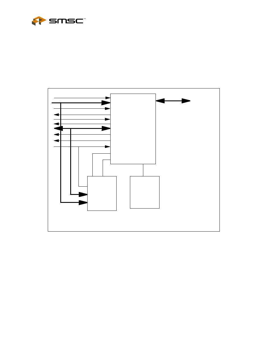
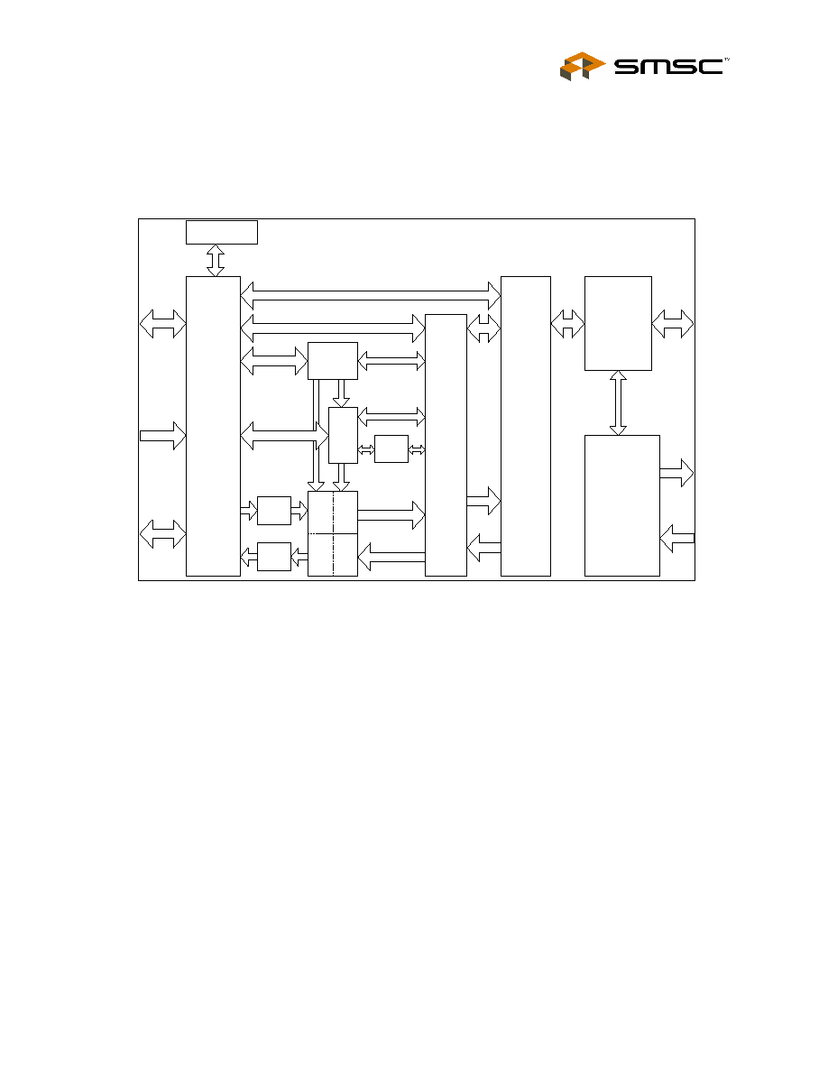
Figure 4.1 - LAN91C96 Internal Block Diagram
DATABU
ADDRES
BUS
CONTROL
BUS
INTERFAC
ARBITE
CSMA/C
ENDE
AUI
MMU
TWISTED
TRANSCEIVE
10BASE-
RAM

Non-PCI Single-Chip Full Duplex Ethernet Controller with Magic Packet
Rev. 09/10/2004
Page 22
SMSC LAN91C965v&3v
DATASHEET
Chapter 5 Functional Description
Except for the bus interface, the functional behavior of the LAN91C96 after initial configuration is identical
for LOCAL BUS and PCMCIA modes.
The LAN91C96 includes an arbitrated shared memory of 6144 bytes. Any portion of this memory can be
used for receive or transmit packets.
The MMU unit allocates RAM memory to be used for transmit and receive packets, using 256 byte pages.
The arbitration is transparent to the CPU in every sense. There is no speed penalty for LOCAL BUS type
of machines due to arbitration. There are no restrictions on what locations can be accessed at any time.
RAM accesses as well as MMU requests are arbitrated.
The RAM is accessed by mapping it into I/O space for sequential access. Except for the RAM accesses
and the MMU request/release commands, I/O accesses are not arbitrated.
The I/O space is 16 bits wide. Provisions for 8 bit systems are handled by the bus interface.
In the system memory space, up to 64 kbytes are decoded by the LAN91C96 as expansion ROM. The
ROM expansion area is 8 bits wide.
Device configuration is done using a serial EEPROM, with support for modifications to the EEPROM at
installation time. A Flash ROM is supported for PCMCIA attribute memory.
The CSMA/CD core implements the 802.3 MAC layer protocol. It has two independent interfaces, the data
path and the control path.
Both interfaces are 16 bits wide. The control path provides a set of registers used to configure and control
the block. These registers are accessible by the CPU through the LAN91C96 I/O space. The data path is
of sequential access nature and typically works in one direction at any given time. An internal DMA type of
interface connects the data path to the device RAM through the arbiter and MMU.
The CSMA/CD data path interface is not accessible to the host CPU.
The internal DMA interface can arbitrate for RAM access and request memory from the MMU when
necessary.
An encoder/decoder block interfaces the CSMA/CD block on the serial side. The encoder will do the
Manchester encoding of the transmit data at 10 Mb/s, while the decoder will recover the receive clock, and
decode received data.
Carrier and Collision detection signals are also handled by this block and relayed to the CSMA/CD block.
The encoder/decoder block can interface the network through the AUI interface pairs, or it can be
programmed to use the internal 10BASE-T transceiver and connect to a twisted pair network.
The twisted pair interface takes care of the medium dependent signaling for 10BASE-T type of networks.
It is responsible for line interface (with external pulse transformers and pre-distortion resistors), collision
detection as well as the link integrity test function. The LAN91C96 provides a 16-bit data path into RAM.
The RAM is private and can only be accessed by the system via the arbiter. RAM memory is managed by
the MMU. Byte and word accesses to the RAM are supported.
If the system to SRAM bandwidth is insufficient the LAN91C96 will automatically use its IOCHRDY line for
flow control. However, for LOCAL BUS, IOCHRDY will never be negated.
Non-PCI Single-Chip Full Duplex Ethernet Controller with Magic Packet
SMSC LAN91C965v&3v
Page 23
Rev. 09/10/2004
DATASHEET
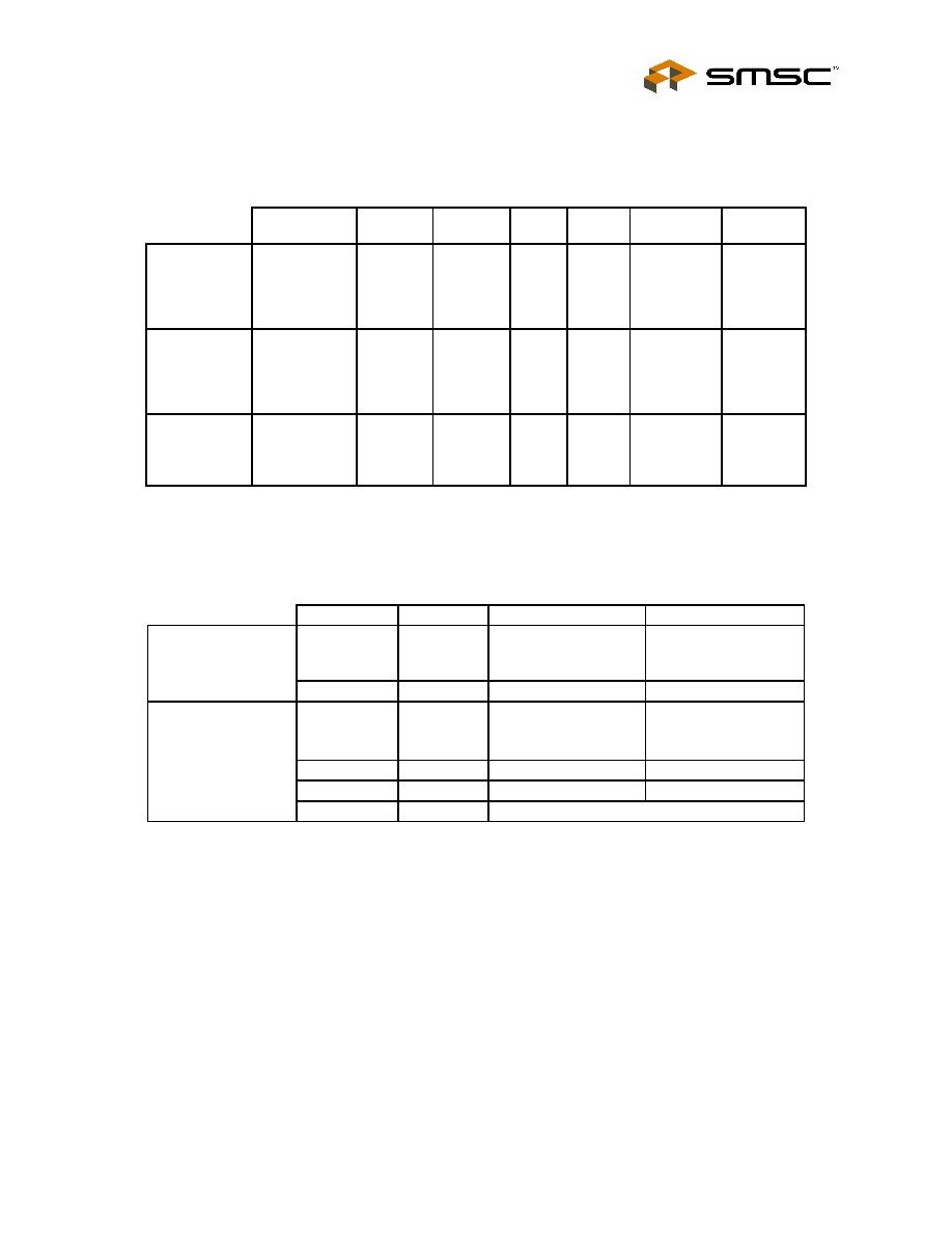
The LAN91C96 consists of an integrated Ethernet controller mapped entirely in I/O space. In addition,
PCMCIA attribute memory space is decoded to interface an external CIS ROM, with configuration registers as
per PCMCIA 3.X extensions (except COR) implemented on-chip in attribute space above the ROM decode
area. The PCMCIA Configuration Registers are accessible in I/O space and also to allow non-PCMCIA dual
function designs.
The Ethernet controller function includes a built-in 6kbyte RAM for packet storage. This RAM buffer is
accessed by the CPU through sequential access regions of 256 bytes each. The RAM access is internally
arbitrated by the LAN91C96, and dynamically allocated between transmit and receive packets. Each packet
may consist of one or more 256 byte page. The Ethernet controller functionality is identical to the LAN91C94
and LAN91C95 except where indicated otherwise.
The LAN91C96 Memory Management Unit parameters are:
RAM SIZE
6kbytes
MAX. NUMBER OF
PAGES
24
MAX. NUMBER OF
PACKETS
24 (FIFOs have 24
entries of 5 bits)
MAX. PAGES PER
PACKET
6
PAGE SIZE
256 bytes
5.1 Buffer
Memory
The logical addresses for RAM access are divided into TX area and RX area.
The TX area is seen by the CPU as a window through which packets can be loaded into memory before
queuing them in the TX FIFO of packets. The TX area can also be used to examine the transmit
completion status after packet transmission.
The RX area is associated to the output of the RX FIFO of packets, and is used to access receive packet
data and status information.
The logical address is specified by loading the address pointer register. The pointer can automatically
increment on accesses.
All accesses to the RAM are done via I/O space.
A bit in the address pointer also specifies if the address refers to the TX or RX area.
In the TX area, the host CPU has access to the next transmit packet being prepared for transmission. In
the RX area, it has access to the first receive packet not processed by the CPU yet.
The FIFO of packets, existing beneath the TX and RX areas, is managed by the MMU. The MMU
dynamically allocates and releases memory to be used by the transmit and receive functions.
Non-PCI Single-Chip Full Duplex Ethernet Controller with Magic Packet
Rev. 09/10/2004
Page 24
SMSC LAN91C965v&3v
DATASHEET
PA
G
E
=
256
b
y
t
e
s
PH
YSI
CA
L
MEM
O
R
Y
TX P
A
C
KET
NU
M
B
E
R
RX
P
A
C
K
ET
NUMB
E
R
MM
U
MM
U
15
36
T
X
ARE
A
1536 RX
AR
E
A
11-
B
I
T
LO
G
I
C
A
L
A
DDR
E
S
S
PO
I
N
T
E
R
RE
GI
S
T
ER
RC
V
BI
T
RC
V VS
.
T
X
AREA
SE
LEC
T
I
O
N
Figure 5.1 ≠ Mapping and Paging vs. Receive and Transmit Area
Non-PCI Single-Chip Full Duplex Ethernet Controller with Magic Packet
SMSC LAN91C965v&3v
Page 25
Rev. 09/10/2004
DATASHEET
B
A
B
C
ST
A
T
U
S
CO
UNT
DA
T
A
ST
A
T
U
S
CO
U
N
T
DA
T
A
P
A
C
KET
#
A
P
A
C
KET
#
B
P
A
CK
ET NUM
BE
R
REGI
S
T
ER
TX
F
I
FO
TO
CS
M
A
L
I
NEA
R
ADD
R
E
S
S
MMU M
A
PPI
N
G
MEM
O
R
Y
CP
U
SID
E
ST
A
T
U
S
CO
U
N
T
DA
T
A
P
A
CKET
#
C
TX C
O
M
P
L
E
T
I
ON
FIFO
FI
FO
P
O
R
T
S
RE
G
I
S
T
E
R
C
Figure 5.2 ≠ Transmit Queues and Mapping
Non-PCI Single-Chip Full Duplex Ethernet Controller with Magic Packet
Rev. 09/10/2004
Page 26
SMSC LAN91C965v&3v
DATASHEET
D
E
D
E
ST
A
T
US
C
O
UNT
DA
T
A
ST
A
T
US
C
O
UNT
DA
T
A
P
A
CKET #D
P
A
CKET
#E
FIFO P
O
R
T
S
R
E
G
I
ST
ER
RX
FI
FO
FR
O
M
CSMA
LI
NE
A
R
A
DDRE
S
S
M
M
U M
A
P
P
I
N
G
ME
M
O
R
Y
CP
U
SID
E
Figure 5.3 ≠ Receive Queues and Mapping
Non-PCI Single-Chip Full Duplex Ethernet Controller with Magic Packet
SMSC LAN91C965v&3v
Page 27
Rev. 09/10/2004
DATASHEET
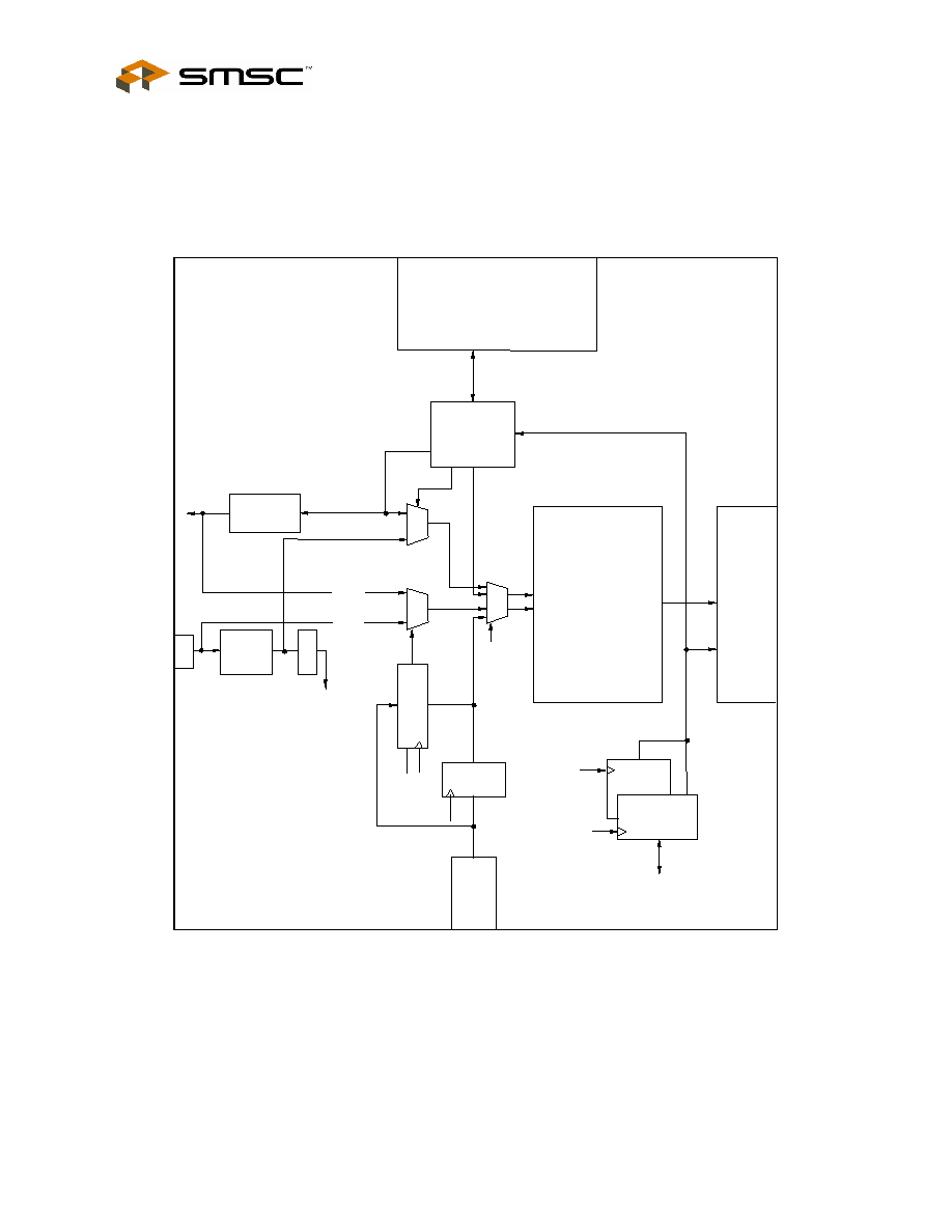
Figure 5.4 - LAN91C96 Internal Block Diagram with Data Path
8-16 bit
Bus
Interface
Unit
Arbiter
DMA
MMU
Ethernet
Protocol
Handler
(EPH)
Twisted Pair
Transceiver
6K Byte
SRAM
WR
FIFO
RD
FIFO
Control
RX Data
TX Data
Control
Control
Address
Data
Control
Control
TX/RX
FIFO
Pointer
TPI
TPO
Control
EEPROM
INTERFACE
TX Data
RX Data
ENDEC
AUI
Non-PCI Single-Chip Full Duplex Ethernet Controller with Magic Packet
Rev. 09/10/2004
Page 28
SMSC LAN91C965v&3v
DATASHEET
T
X
F
I
F
O
T
X
C
O
M
P
L
E
T
I
O
N
F
I
F
O
P
N
R
R
X
F
I
F
O
P
A
C
K
E
T
N
U
M
B
E
R
T
X
(
P
A
C
K
E
T
N
U
M
B
E
R
R
E
G
)
R
C
V
P
O
I
N
T
E
R
R
E
G
I
S
T
E
R
&
C
O
U
N
T
E
R
L
O
A
D
I
N
C
R
X
F
I
F
O
R
E
A
D
P
O
I
N
T
E
R
L
A
T
C
H
P
O
I
N
T
E
R
R
E
G
I
S
T
E
R
P
A
C
K
E
T
#
A
D
D
R
E
S
S
D
M
A
D
A
T
A
C
S
M
A
/
C
D
C
P
U
/
n
L
A
N
(
F
R
O
M
A
R
B
I
T
E
R
)
L
O
G
I
C
A
L
A
D
D
R
E
S
S
P
A
C
K
E
T
#
M
M
U
P
H
Y
S
I
C
A
L
A
D
D
R
E
S
S
D
A
T
A
A
D
D
R
E
S
S
W
R
I
T
E
R
E
G
R
E
A
D
R
E
G
W
R
I
T
E
D
A
T
A
R
A
M
D
A
T
A
R
E
G
I
S
T
E
R
(
F
I
F
O
S
)
R
E
A
D
D
A
T
A
T
/
n
R
Figure 5.5 ≠ Logical Address Generation and Relevant Registers
Non-PCI Single-Chip Full Duplex Ethernet Controller with Magic Packet
SMSC LAN91C965v&3v
Page 29
Rev. 09/10/2004
DATASHEET
Table 5.1 - LAN91C96 Address Space
SIGNALS
USED
LOCAL
BUS
PCMCIA 68000
ON-
CHIP
DEPTH WIDTH
PCMCIA
Attribute
Memory
nOE, nWE
N
Y
N
N
(extern
al
ROM)
Up to 32k
locations,
only even
bytes are
usable
8 bits on
even
addresses
PCMCIA
Configuration
Registers
nOE, nWE
N
Y
N
Y
64
locations,
only even
bytes are
usable
8 bits
Ethernet I/O
space
(Note 5.1)
nIORD/
nIOWR (68K:
xDS, R/nW)
Y Y
Y
Y
16
locations
8 or 16
bits
(68K: 16
bits only)
Note 5.1
This space also allows access to the PCMCIA Configuration Register through Bank 4.
Table 5.2 - Bus Transactions In LOCAL BUS Mode
A0
NSBHE
D0-7 D8-15
8 BIT MODE
((nEN16=1)
(16BIT=0))
0 X Even
byte
-
1
X
Odd
byte
-
16 BIT MODE
otherwise
0
0
Even byte
Odd byte
0
1
Even
byte
-
1
0
-
Odd
byte
1
1
Invalid
cycle
Non-PCI Single-Chip Full Duplex Ethernet Controller with Magic Packet
Rev. 09/10/2004
Page 30
SMSC LAN91C965v&3v
DATASHEET
Table 5.3 - Bus Transactions In PCMCIA Mode
A0
NCE1
NCE2 D0-7
D8-15
8 BIT MODE
((IOis8=1) +
(nEN16=1).
(16BIT=0))
0 0
X
Even
byte
-
1
0
X
Odd
byte
-
X
1
X
NO
CYCLE
16 BIT MODE
otherwise
0
0
0
Even byte
Odd byte
0
0
1
Even
byte
-
1
0
1
Odd
byte
X
1
0
-
Odd
byte
X
1
1
NO
CYCLE
Table 5.4 - Bus Transactions In 68000 Mode
D0-7
D8-15
8 BIT MODE
ILLEGAL ACCESS
16 BIT MODE
(A0=0).(nSBHE=0)
Even byte
Odd byte
16BIT:
CONFIGURATION REGISTER bit 7
IOis8:
CSR register bit 5
nEN16:
pin nEN16
8 Bit mode:
((IOis8 = 1) + (nMIS16 = 1)
5.2 Interrupt
Structure
The Ethernet interrupt is conceptually equivalent to the LAN91C94 interrupt line, it is the or function of all
enabled interrupts within the Ethernet core. The enabling, reporting, and clearing of these sources is
controlled by the ECOR register. The interrupt structure is similar for LOCAL BUS and PCMCIA modes
with the following exceptions:
PCMCIA uses a single interrupt pin (nIREQ) while LOCAL BUS can use any of four INTR0-3 pins.
Non-PCI Single-Chip Full Duplex Ethernet Controller with Magic Packet
SMSC LAN91C965v&3v
Page 31
Rev. 09/10/2004
DATASHEET
Table 5.5 - Interrupt Merging
FUNCTION
PCMCIA MODE
LOCAL BUS MODE
Interrupt Output
nIREQ when function is Ready.
Acts as ready line at power up.
I.e. remains low until the chip
(therefore, card) is Ready
INTR0-3
Ethernet Interrupt Source
OR function of all interrupt bits specified in the Interrupt Status Register
ANDed with their respective Enable bits
Ethernet Interrupt Enable
Not Applicable in LOCAL BUS
mode
Ethernet Interrupt Status Bit
Intr bit in ECSR
5.3 Reset
Logic
The pins and bits involved in the different reset mechanisms are:
RESET - Input Pin
SRESET - Soft Reset bit in ECOR, or the SRESET bit
SOFT RST - EPH Soft Reset bit in RCR
RESETS THE FOLLOWING
FUNCTIONS
SAMPLES
LOCAL BUS
VS. PCMCIA
MODE
TRIGGERS
EEPROM
READ
RESET pin
All internal logic
Yes
Yes
ECOR
Register
SRESET bit
The Ethernet controller function and
Ethernet PCMCIA Configuration Registers
except for the bit itself. Setting this bit also
lowers the nIREQ/READY line. When
cleared, the nIREQ/READY line is raised.
No Yes
SOFT RST
The Ethernet controller itself except for
the IA, CONF and BASE registers. It does
not reset any PCMCIA Configuration
Register.
No No
5.4
Power Down Logic States
Table 5.6, Table 5.7, Table 5.8, and Table 5.9 describe the power down states of the LAN91C96. The
pins and bits involved in power down are:
1.
PWRDWN/TXCLK - Input pin valid when XENDEC is not zero (0).
2.
Pwrdwn bits in ECSR
3.
Enable Function bit in ECOR
4.
PWRDN - Legacy power down bit in Control Register.
Non-PCI Single-Chip Full Duplex Ethernet Controller with Magic Packet
Rev. 09/10/2004
Page 32
SMSC LAN91C965v&3v
DATASHEET
5.5
LAN91C96 Power Down States
Table 5.6 - LOCAL BUS Mode Defined States (Refer To Table 5.7 For Next States To Wake-Up Events)
CURRENT STATE
NO.
PWRDWN PIN
(A= ASSRTD)
ECOR
FUNCTION
ENABLE
ECSR
POWER
DOWN
CTR
PWRDW
N BIT
CTR
WAKEU
P_EN
BIT
POWERS DOWN
DOES NOT
POWER
DOWN
1 A
X X
X X
Everything.
Asserts the
modem power
down pin
(nPWDN) also
2 nA
X 0 0 0
Ethernet Tx,
Rx, Link
3 nA
X 0 0 1
Ethernet
Tx
Ethernet Rx,
Link
4 nA
X 0 1 1
Ethernet Tx, Rx,
Link
5 nA
X 0 1 0
Ethernet Tx, Rx,
Link
Notes:
The chart assumes that ECOR Function Enable bit is meaningless in LOCAL BUS mode.
ECSR Power Down bit must not be set to one(1) in LOCAL BUS mode.
Table 5.7- LOCAL BUS Mode
NEXT STATE
NO.
WAKES UP BY
PWR DWN PIN
(A=ASSRTD)
ECOR
FUNCTION
ENABLE
ECSR
POWER
DOWN
CTR
PWR-
DWN BIT
CTR
WAKEUP_
EN BIT
COMMENTS
..1
PWRDWN Pin
deassertion
nA No
change
No
change
No
change
No change
ECOR
Function
Enable Bit
value is
meaningless
in LOCAL
BUS mode
..2
nA
X
0
0
0
Fully
Awake
..3
By writing a 0 to CTR
WAKEUP_EN bit
nA X
0
0
0
..4
By writing a 0 to CTR
WAKEUP_EN bit
AND CTR PWRDWN
bit = 0
nA X
0
0
0
The CTR
PWRDWN bit
has
precedence
unlike the
LAN91C95
..5
By writing 0 to CTR
PWRDWN bit
nA X
0
0
0
Notes:
The chart assumes that ECOR Function Enable bit is meaningless in LOCAL BUS mode.

Non-PCI Single-Chip Full Duplex Ethernet Controller with Magic Packet
SMSC LAN91C965v&3v
Page 33
Rev. 09/10/2004
DATASHEET
ECSR Power Down bit must not be set to one (1) in LOCAL BUS mode.
Table 5.8 - PCMCIA Mode (Refer To Table 5.7 For Next States To Wake-Up Events)
CURRENT STATE
NO.
PWRDWN
PIN
(A=ASSRTD)
ECOR
FUNC
ENABLE
ECSR
PWR
DOWN
CTR
PWR
DWN
BIT
CTR
WAKEUP_E
N BIT
POWERS
DOWN
DOES NOT POWER
DOWN
1 A X
X
X
X
Everything.
Asserts the
modem power
down pin
(nPWDN)
also
2 nA 1
0
0 0
Ethernet Tx, Rx,
Link; PCMCIA
Att/Config Mem
3 nA 1
0
0 1
Ethernet
Tx
Ethernet Rx, Link;
PCMCIA Att/Config
Mem
4 nA 1
0
1 1
Ethernet Tx,
Rx
1
, Link
1
PCMCIA Att/Conf
Memory
5 nA 0
X
X 0
Ethernet Tx,
Rx, Link
PCMCIA Att/Conf
Memory
6 nA 0
X
X 1
Ethernet Tx,
Rx
1
, Link
1
PCMCIA Att/Conf
Memory
7 nA 1
1
0 0
Ethernet Tx,
Rx, Link
PCMCIA Att/Config
Mem
7S nA 1 1
1 0
Ethernet Tx,
Rx, Link
PCMCIA Att/Config
Mem
8 nA 1
1
0 1
Ethernet Tx,
Rx
1
, Link
1
PCMCIA Att/Config
Mem
8S nA 1 1
1 1
Ethernet Tx,
Rx
1
, Link
1
PCMCIA Att/Config
Mem
Note
1
:
The LAN91C96 implementation is different from the LAN91C95; the LAN91C96 powers down the Ethernet
Rx and Link logic also, whereas, the LAN91C95 does not.
Table 5.9 - PCMCIA Mode
NEXT
STATE
NO.
WAKES UP BY
PWR DWN PIN
(A= ASSRTD)
ECOR
FUNC
ENABLE
ECSR
PWR
DOWN
CTR
PWRDWN
BIT
CTR
WAKEUP_EN
BIT
COMMENTS
1
PWRDWN Pin
deassertion
nA
No
change
No
change
No change
No change
Pin deassertion
will make the
Att/Conf Mem
accessible
entirely
2
nA
1
0
0
0
Fully
Awake
3
By writing a 0 to
CTR WAKEUP_EN
bit
nA 1
0
0 0

Non-PCI Single-Chip Full Duplex Ethernet Controller with Magic Packet
Rev. 09/10/2004
Page 34
SMSC LAN91C965v&3v
DATASHEET
NEXT
STATE
NO.
WAKES UP BY
PWR DWN PIN
(A= ASSRTD)
ECOR
FUNC
ENABLE
ECSR
PWR
DOWN
CTR
PWRDWN
BIT
CTR
WAKEUP_EN
BIT
COMMENTS
4
By writing a 0 to
CTR PWRDWN and
0 to WAKEUP_EN
bits
nA 1
0
0 0
5
By writing 1 to
ECOR Func Enable,
0 to ECSR Power
Down, 0 to CTR
PWRDWN
nA 1
0
0 0
Note: Both
Power down
bits need to be
written as 0
only if both
were set to 1
6
By writing 1 to
ECOR Func Enable,
0 to ECSR Power
Down, 0 to CTR
PWRDWN, and 0 to
WAKEUP_EN bit
nA 1
0
0 0
Note: Both
Power down
bits need to be
written as 0
only if both
were set to 1
7
By writing 0 to
ECSR Power Down
bit*
nA 1
0
0 0
7S
By writing 0 to
ECSR Power Down
and a 0 to CTR
PWRDWN bit
nA 1
0
0 0
Note: Both
Power down
bits need to be
written as 0
only if both
were set to 1
8
By writing 0 to
ECSR Power Down
and writing CTR
PWRDWN bit = 0 &
WAKEUP_EN = 0, if
needed
nA 1
0
0 0
8S
By writing 0 to
ECSR Power Down
and writing CTR
PWRDWN bit = 0 &
WAKEUP_EN = 0, if
needed
nA 1
0
0 0
PCMCIA Attribute Memory
Address 0- 7FFEh
The Attribute Memory is implemented using an external parallel EEPROM, ROM or Flash ROM. A parallel
EEPROM (or equivalent external device) must be used for CIS.
In LOCAL BUS mode, serial EEPROM is used for configuration and IEEE Node address making it software
compatible to the LAN9xxx family of Ethernet LAN Controllers. The EEPROM is optional for both LOCAL BUS
and PCMCIA requiring a Minimum size of 64 X 16 bit word addresses.
The LAN91C96 generates the appropriate control lines (nFCS and nFWE) to read and write the Attribute
memory, and it tri-states the data bus during external Attribute Memory accesses. Only even locations are
used.

Non-PCI Single-Chip Full Duplex Ethernet Controller with Magic Packet
SMSC LAN91C965v&3v
Page 35
Rev. 09/10/2004
DATASHEET
PCMCIA Configuration Registers
Address 8000-8003h
The PCMCIA Configuration Registers are stored inside the LAN91C96 above the external Attribute
Memory address space. These registers are used to configure and control the PCMCIA related
functionality of the Ethernet. These registers are eight bit wide and reside on even locations. The
LAN91C96 will ignore odd access to this area and ignore writes. The device will read zero's on odd
access. This address offset has changed from prior LAN9XXX PCMCIA Family designs to allow a larger
address range for other attribute memory data. This data could be a larger card information structure or a
XIP data image.
Attribute Memory map
The EPROM attribute memory decodes are shown below. Internal to the LAN91C96, the memory
addressing logic will allow byte or word access on even byte boundaries. LAN91C96 uses address A0-9,
A15, along with nREG, nCE1, nWE and nOE. An on odd byte address access (A0=1), the LAN91C96 will
generate a arbitrary value of Zero (0) since the PCMCIA specification states that the high byte of a word
access in attribute memory is a don't care. This allows backward compatibility to 8 bit hosts.
With or Without 64x16 bit Serial EEPROM:
ATTRIBUTE MEMORY
ADDRESS
EXTERNAL EPROM
STORE
CONFIGURATIO
N REGISTERS
0 - 7FFEh
X
8000h - 8003h
X
5.6 PCMCIA
CONFIGURATION REGISTERS DESCRIPTION
Ethernet Function (Base Address 8000h)
8000h - Ethernet Configuration Option Register (ECOR)
7
6 5 4 3 2 1 0
SRESET
LevIREQ
(Read
only)
0 WR
ATTRIB
Enable
Function
0
1 0 0 0 0 0 0
BIT 7 - SRESET: This bit when set will clear all internal registers associated with the Ethernet function
except itself and it will also lower the nIREQ/READY pin. When this bit is cleared, nIREQ/READY pin will
be raised.
BIT 6 - LevIREQ: This bit is read only and reads as a one to indicate level mode interrupts are used.
Pulse mode interrupts are not supported.
BIT 5, 4, 3 - Not defined
BIT 2 - WRATTRIB: This bit when set (1) allows writing into the external attribute memory space.
BIT 1 - Not Defined
BIT 0 - Enable Function: This bit enables (1) or disables (0) the Ethernet function. While the Ethernet
function is disabled it remains in power down mode, no access to the Ethernet I/O space (i.e. The bank

Non-PCI Single-Chip Full Duplex Ethernet Controller with Magic Packet
Rev. 09/10/2004
Page 36
SMSC LAN91C965v&3v
DATASHEET
register are not accessible) is allowed. IREQ is not generated for this function and INPACK* is not
returned for accesses to the Ethernet registers.
Note:
Magic packet bit setting is ignored if the function is disabled.
8002h - Ethernet Configuration and Status Register (ECSR)
7 6 5 4 3
2
1 0
IOIs8
Pwrdwn
Intr
0 0 0 0 0
0
0 0
BIT 7 - Not defined
BIT 6 - Not defined
BIT 5 - IOIs8: This bit when set, indicates that the Host can only do 8 bit cycles (on D7-0). The Ethernet
function is forced in this case to eight bit mode regardless of the EN16* pin and 16BIT value. This bit also
disables (floats) the IOIs16 signal.
BIT 4 - Not defined
BIT 3 - Not defined
BIT 2 - PwrDwn: When set (1), this bit puts the LAN91C96 Ethernet function into power down mode. The
Ethernet function is also put into power down mode when the Enable Function bit (ECOR bit 0 in PCMCIA
only) is cleared. Refer to the Power Down Logic section for additional information.
BIT 1 - Intr: This bit is read/set to a one when this function is requesting interrupt service. When this bit is
set, IREQOut is asserted.
BIT 0 - Not Defined
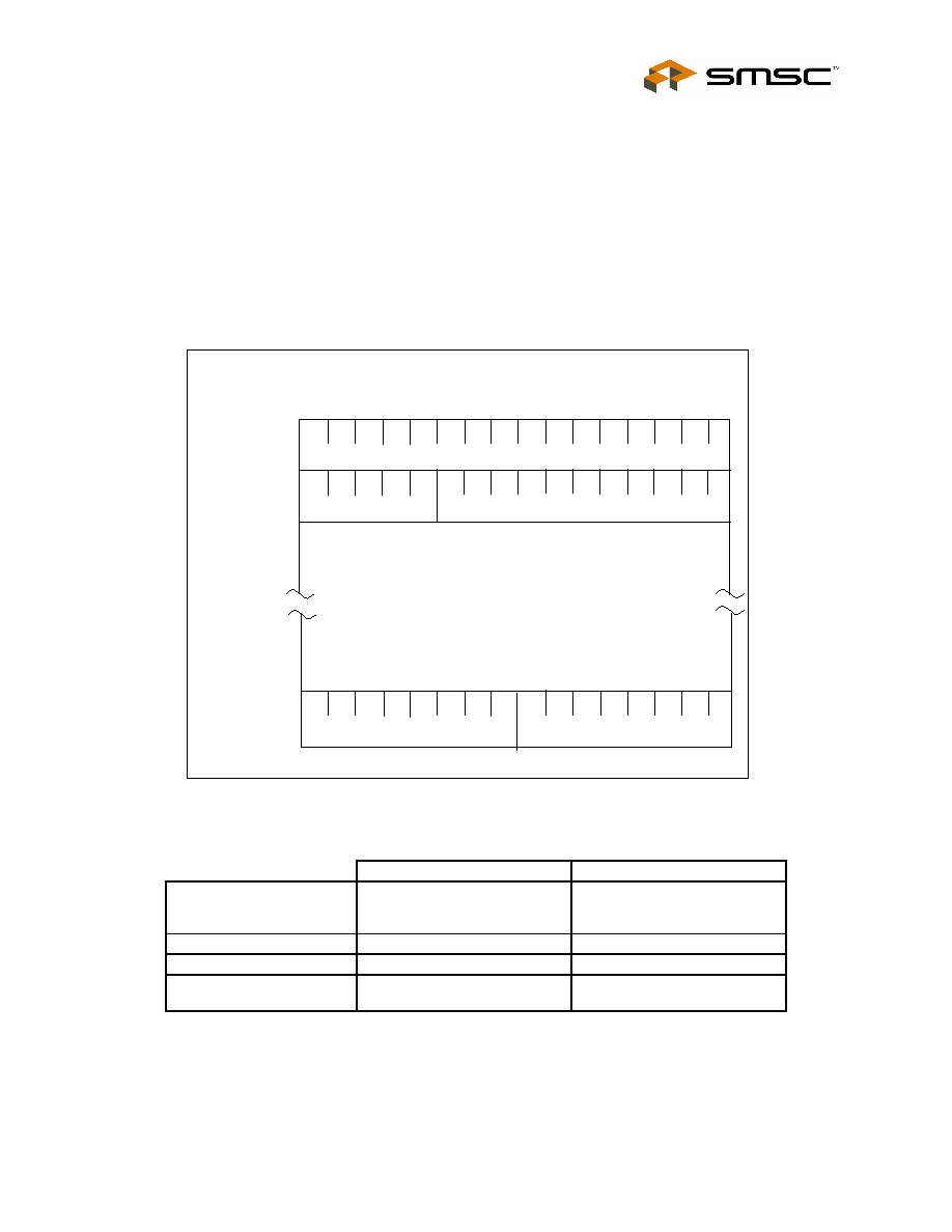
Non-PCI Single-Chip Full Duplex Ethernet Controller with Magic Packet
SMSC LAN91C965v&3v
Page 37
Rev. 09/10/2004
DATASHEET
Chapter 6 Frame Format in Buffer Memory for
Ethernet
The frame format in memory is similar to that in the TRANSMIT and RECEIVE areas. The first word is
reserved for the status word, the next word is used to specify the total number of bytes, and that in turn is
followed by the data area. The data area holds the packet itself, and its length is determined by the byte
count. The frame memory format is word oriented.
Figure 6.1 ≠ Data Frame Format
TRANSMIT PACKET
RECEIVE PACKET
STATUS WORD
Written by CSMA upon transmit
completion (see Status Register)
Written by CSMA upon receive
completion (see RX Frame
Status Word)
BYTE COUNT
Written by CPU
Written by CSMA
DATA AREA
Written/modified by CPU
Written by CSMA
CONTROL BYTE
Written by CPU to control
ODD/EVEN data bytes
Written by CSMA. Also has
ODD/EVEN bit
BYTE COUNT - Divided by two, it defines the total number of words, including the STATUS WORD, the
BYTE COUNT WORD, the DATA AREA and the CONTROL BYTE. The receive byte count always
appears as even, the ODDFRM bit of the receive status word indicates if the low byte of the last word is
RESERVED
BYTE COUNT (always even)
STATUS WORD
DATA AREA
LAST DATA BYTE (if odd)
bit0
bit15
RAM
OFFSET
(DECIMAL)
0
2
4
1534 Max
CONTROL BYTE
Last Byte
1st Byte
2nd Byte
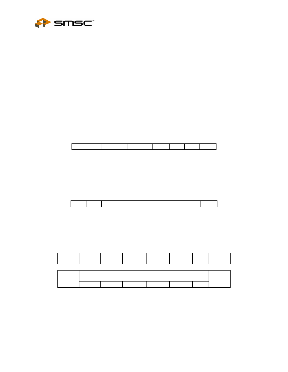
Non-PCI Single-Chip Full Duplex Ethernet Controller with Magic Packet
Rev. 09/10/2004
Page 38
SMSC LAN91C965v&3v
DATASHEET
relevant. The transmit byte count least significant bit will be assumed 0 by the controller regardless of the
value written in memory. The maximum size of the frame can be stored in 6 pages (256 bytes per page),
the maximum BYTE COUNT number is 1536.
DATA AREA (in RAM)
The data area starts at offset 4 of the packet structure, and it can extend for up to 1531 bytes. The data
area contains six bytes of DESTINATION ADDRESS followed by six bytes of SOURCE ADDRESS,
followed by a variable length number of bytes.
On transmit, all bytes are provided by the CPU, including the source address. The LAN91C96 does not
insert its own source address. On receive, all bytes are provided by the CSMA side.
The 802.3 Frame Length word (Frame Type in Ethernet) is not interpreted by the LAN91C96. It is treated
transparently as data for both transmit and receive operations.
CONTROL BYTE (in RAM)
The CONTROL BYTE always resides on the high byte of the last word. For transmit packets the
CONTROL BYTE is written by the CPU as:
X X ODD CRC 0 0 0 0
ODD - If set, indicates an odd number of bytes, with the last byte being right before the CONTROL BYTE.
If clear, the number of data bytes is even and the byte before the CONTROL BYTE is not transmitted.
CRC - When set, CRC will be appended to the frame. This bit has only meaning if the NOCRC bit in the
TCR is set.
For receive packets the CONTROL BYTE is written by the controller as:
0
1
ODD 0 0 0 0 0
ODD - If set, indicates an odd number of bytes, with the last byte being right before the CONTROL BYTE.
If clear, the number of data bytes is even and the byte before the CONTROL BYTE should be ignored.
RECEIVE FRAME STATUS WORD (in RAM)
This word is written at the beginning of each receive frame in memory. It is not available as a register.
ALGN
ERR
BROD
CAST
BADCRC ODDFRM TOOLNG
TOO
SHORT
HASH
VALUE
MULT
CAST
5 4 3 2 1
0
ALGNERR - Frame had alignment error.
BRODCAST - Receive frame was broadcast.
BADCRC - Frame had CRC error.
Non-PCI Single-Chip Full Duplex Ethernet Controller with Magic Packet
SMSC LAN91C965v&3v
Page 39
Rev. 09/10/2004
DATASHEET
ODDFRM - This bit when set indicates that the received frame had an odd number of bytes.
TOOLNG - The received frame is longer than the 802.3 maximum size (1518 bytes on the cable).
TOOSHORT - The received frame is shorter than the 802.3 minimum size (64 bytes on the cable).
HASH VALUE - Provides the hash value used to index the Multicast Registers. Can be used by receive
routines to speed up the group address search. The hash value consists of the six most significant bits of
the CRC calculated on the Destination Address, and maps into the 64 bit multicast table. Bits 5,4,3 of the
hash value select a byte of the multicast table, while bits 2,1,0 determine the bit within the byte selected.
Examples of the address mapping are shown in the table below:
ADDRESS
HASH VALUE 5-0
MULTICAST TABLE BIT
ED 00 00 00 00 00
0D 00 00 00 00 00
01 00 00 00 00 00
2F 00 00 00 00 00
000 000
010 000
100 111
111 111
MT-0 bit 0
MT-2 bit 0
MT-4 bit 7
MT-7 bit 7
MULTCAST - Receive frame was multicast. If hash value corresponds to a multicast table bit that is set,
and the address was a multicast, the packet will pass address filtering regardless of other filtering criteria.
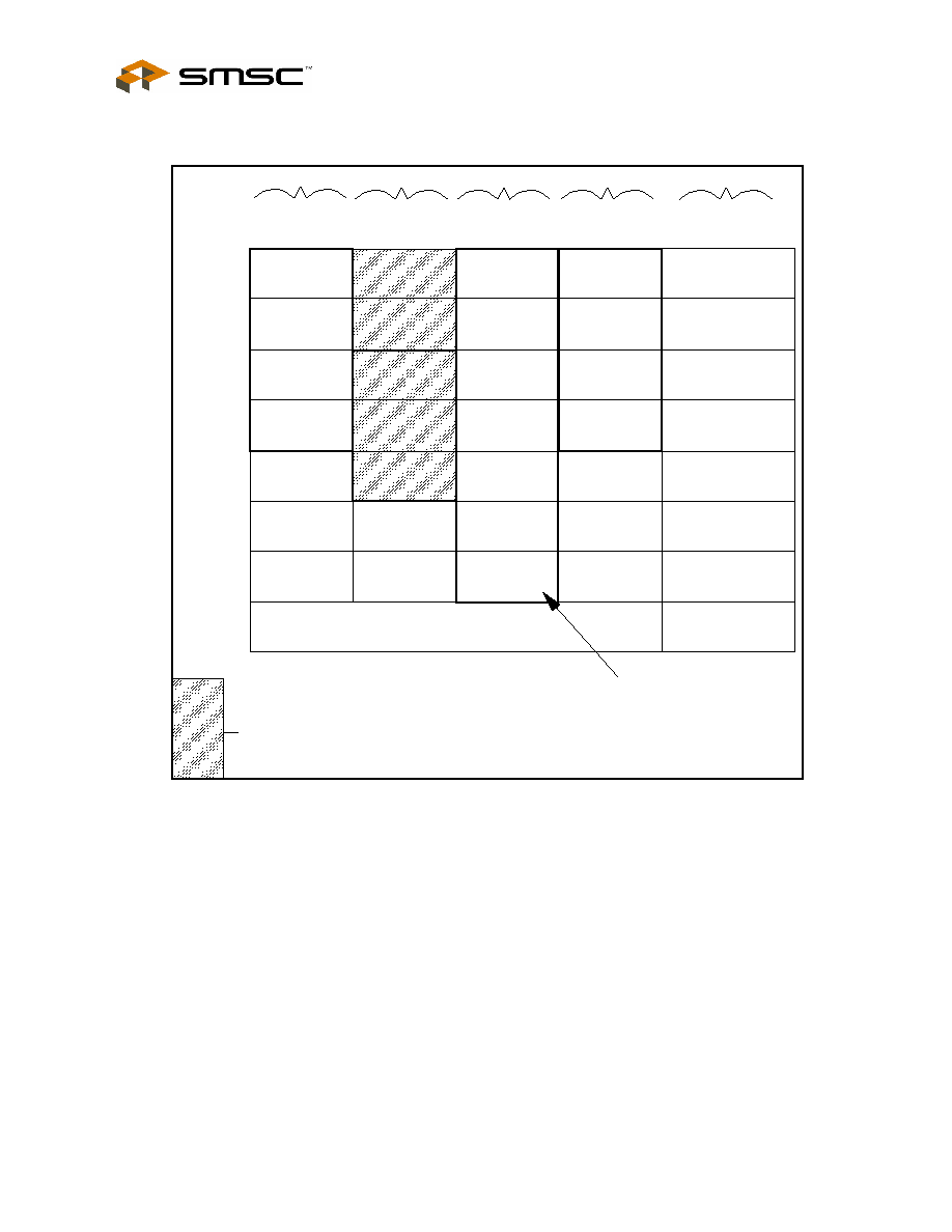
Non-PCI Single-Chip Full Duplex Ethernet Controller with Magic Packet
Rev. 09/10/2004
Page 40
SMSC LAN91C965v&3v
DATASHEET
Figure 6.2 - LAN91C96 Registers
BANK0
BANK1
BANK2
BANK3
0
2
4
6
8
A
C
E
TCR
EPH STATUS
RCR
COUNTER
MIR
MCR
BANK SELECT REGISTER
CONFIG
BASE
(INDIVIDUAL
ADDRESS)
GENERAL
PURPOSE
CONTROL
MMU
COMMAND
PNR
ARR
FIFO PORTS
POINTER
DATA
DATA
INTERRUPT
MULTICAST
TABLE
Non volatile,
stored in EEPROM.
BANK2 Register
used during
run time.
16 Bit Registers 16 Bit Registers 16 Bit Registers 16 Bit Registers
RESERVED
MGMT
REVISION
ERCV
BANK4
16 Bit Registers
ECOR (LOW BYTE)
ECSR (HIGH BYTE)
BANK SELECT
IA 0-1
IA 2-3
IA 4-5
Non-PCI Single-Chip Full Duplex Ethernet Controller with Magic Packet
SMSC LAN91C965v&3v
Page 41
Rev. 09/10/2004
DATASHEET
Chapter 7 Registers Map in I/O Space
7.1
I/O Space Access
The address is determined by the Ethernet I/O Base Registers. The Ethernet I/O space can be configured
as an 8 or 16 bit I/O space, and is similar to the LAN91C94, LAN91C92, etc. I/O space mapping. To limit
the I/O space requirements to 16 locations, the registers are Split into 4 banks in LOCAL BUS mode and 5
banks in PCMCIA mode. The last word of the I/O area is shared by all banks and can be used to change
the bank in use. Banks 0 through 3 functionally correspond to the LAN91C94 banks, while Bank 4 allows
access to the PCMCIA registers in LOCAL BUS mode.
Registers are described using the following convention:
OFFSET NAME
TYPE
SYMBOL
E
BANK SELECT
REGISTER
READ/WRITE
BSR
BIT 15
BIT14
BIT 13
BIT 12
BIT 11
BIT 10
BIT9
BIT8
RST
Val
RST
Val
RST
Val
RST
Val
RST
Val
RST
Val
RST
Val
RST
Val
BIT 7
BIT 6
BIT 5
BIT 4
BIT 3
BIT 2
BIT 1
BIT 0
RST
Val
RST
Val
RST
Val
RST
Val
RST
Val
RST
Val
RST
Val
RST
Val
OFFSET - Defines the address offset within the IOBASE where the register can be accessed at, provided
the bank select has the appropriate value. The offset specifies the address of the even byte (bits 0-7) or
the address of the complete word. The odd byte can be accessed using address (offset + 1).
Some registers (e.g. the Interrupt Ack. or the Interrupt Mask) are functionally described as two eight bit
registers. In such case, the offset of each one is independently specified.
Regardless of the functional description, when the LAN91C96 is in 16 bit mode, all registers can be
accessed as words or bytes.
RST Val - The default bit values upon hard reset are highlighted below each register.
7.2
I/O Space Registers Description
(Bank 4 Registers are described under PCMCIA Configuration Registers and will not be described again).
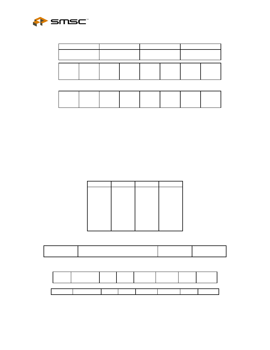
Non-PCI Single-Chip Full Duplex Ethernet Controller with Magic Packet
Rev. 09/10/2004
Page 42
SMSC LAN91C965v&3v
DATASHEET
BANK SELECT REGISTER
OFFSET
NAME
TYPE
SYMBOL
# in HEX
BANK SELECT
REGISTER
READ/WRITE
BSR
0
0
1
1
0
0
1
1
0 0 1 1 0 0 1 1
BS2
BS1
BS0
X X X X X 0 0 0
BS2, BS1, BS0 - Determine the bank presently in use.
This register is always accessible except in power down mode and is used to select the register bank in
use.
The upper byte always reads as 33h and can be used to help determine the I/O location of the LAN91C96.
The BANK SELECT REGISTER is always accessible regardless of the value of BS0-2.
The LAN91C96 implements only 5 banks in both PCMCIA and LOCAL BUS mode, therefore accesses to
non-existing banks will ignore writes and reads will return 0x33 on byte reads. All 5 banks are accessible
in both LOCAL BUS and PCMCIA mode.
BS2 BS1 BS0
BANK
#
0
0
0
0
1
1
1
1
0
0
1
1
0
0
1
1
0
1
0
1
0
1
0
1
0
1
2
3
4
None
None
None
I/O SPACE - BANK0
OFFSET NAME TYPE
SYMBOL
0
TRANSMIT CONTROL REGISTER READ/WRITE TCR
This register holds bits programmed by the CPU to control some of the protocol transmit options.
FDSE ETEN-TYPE
EPH
LOOP
STP
SQET
FDUPLX
MON_
CSN
NOCRC
0 0
0
0
0
0
X
0
PAD_EN
TXP_EN
FORCOL
LOOP
TXENA
0 X
X
X
0
0
0
0

Non-PCI Single-Chip Full Duplex Ethernet Controller with Magic Packet
SMSC LAN91C965v&3v
Page 43
Rev. 09/10/2004
DATASHEET
NOCRC - Does not append CRC to transmitted frames when set, allows software to insert the desired
CRC. Defaults to zero, namely CRC inserted.
FDSE - Full Duplex Switched Ethernet. When set, the LAN91C96 is configured for Full Duplex Switched
Ethernet, it defaults clear to normal CSMA/CD protocol. In FDSE mode the LAN91C96 transmit and
receive processes are fully independent, namely no deferral and no collision detection are implemented.
When FDSE is set, FDUPLX is internally assumed high and MON_CSN is assumed low regardless of their
actual values.
ETEN-TYPE - Early transmit underrun function type. When low, ETEN bit in the PTR register will enable
the Early transmit underrun function as it was implemented in the LAN91C94. I.e. "The Early Transmit
function allows the CPU to enqueue the first transmit packet before it is fully loaded in packet memory.
The loading operation proceeds in parallel with the transmission, and in the case that the transmitter gets
ahead of the CPU, the LAN91C96 will prevent the transmission of erroneous data by forcing an Underrun
condition. Underruns will be triggered by starving the transmit DMA if the LAN91C96 detects that the DMA
TX address exceeds the pointer address."
With ETEN-TYPE set to one (1), ETEN bit set to one(1) in the pointer register will mean the following:
"For underrun detection purposes the RAM logical address and packet numbers of the packet being
loaded are compared against the logical address and packet numbers of the packet being transmitted. If
the packet numbers match and the logical address of the packet being transmitted exceeds the address
being loaded, the LAN91C96 will prevent the transmission of erroneous data by forcing an Underrun
condition. Underruns will be triggered by starving the transmit DMA if the LAN91C96 detects that the DMA
TX address exceeds the pointer address."
Note:
The bit may be available for chips with Rev. ID 6 only and may be assigned to a different function in the
future.
EPH_LOOP - Internal loopback at the EPH block. Does not exercise the encoder decoder. Serial data is
looped back when set. Defaults low. Note: After exiting the loopback test, an SRESET in the ECOR or the
SOFT_RST in the RCR must be set before returning to normal operation.
STP_SQET - Stop transmission on SQET error. If set, stops and disables transmitter on SQE test error.
Does not stop on SQET error and transmits next frame if clear. Defaults low.
FDUPLX - When set it enables full duplex operation. This will cause frames to be received if they pass the
address filter regardless of the source for the frame. When clear the node will not receive a frame sourced
by itself. Clearing this bit (Normal Operation), allows in promiscuous mode, not to receive it's own packet.
TXP_EN - This bit is reserved and should always be set to 0 on the LAN91C96.
MON_CSN - When set the LAN91C96 monitors carrier while transmitting. It must see its own carrier by the
end of the preamble. If it is not seen, or if carrier is lost during transmission, the transmitter aborts the
frame without CRC and turns itself off.
When this bit is clear the transmitter ignores its own carrier. Defaults low.
PAD_EN - When set, the LAN91C96 will pad transmit frames shorter than 64 bytes with 00. For TX, CPU
should write the actual BYTE COUNT before padded by the LAN91C96 to the buffer RAM, excludes the
padded 00. When this bit is cleared, the LAN91C96 does not pad frames.
FORCOL - When set the transmitter will force a collision by not deferring deliberately. After the collision
this bit is reset automatically. This bit defaults low to normal operation.
LOOP - Local Loopback. When set, transmit frames are internally looped to the receiver after the
encoder/decoder. Collision and Carrier Sense are ignored. No data is sent out. Defaults low to normal
mode.
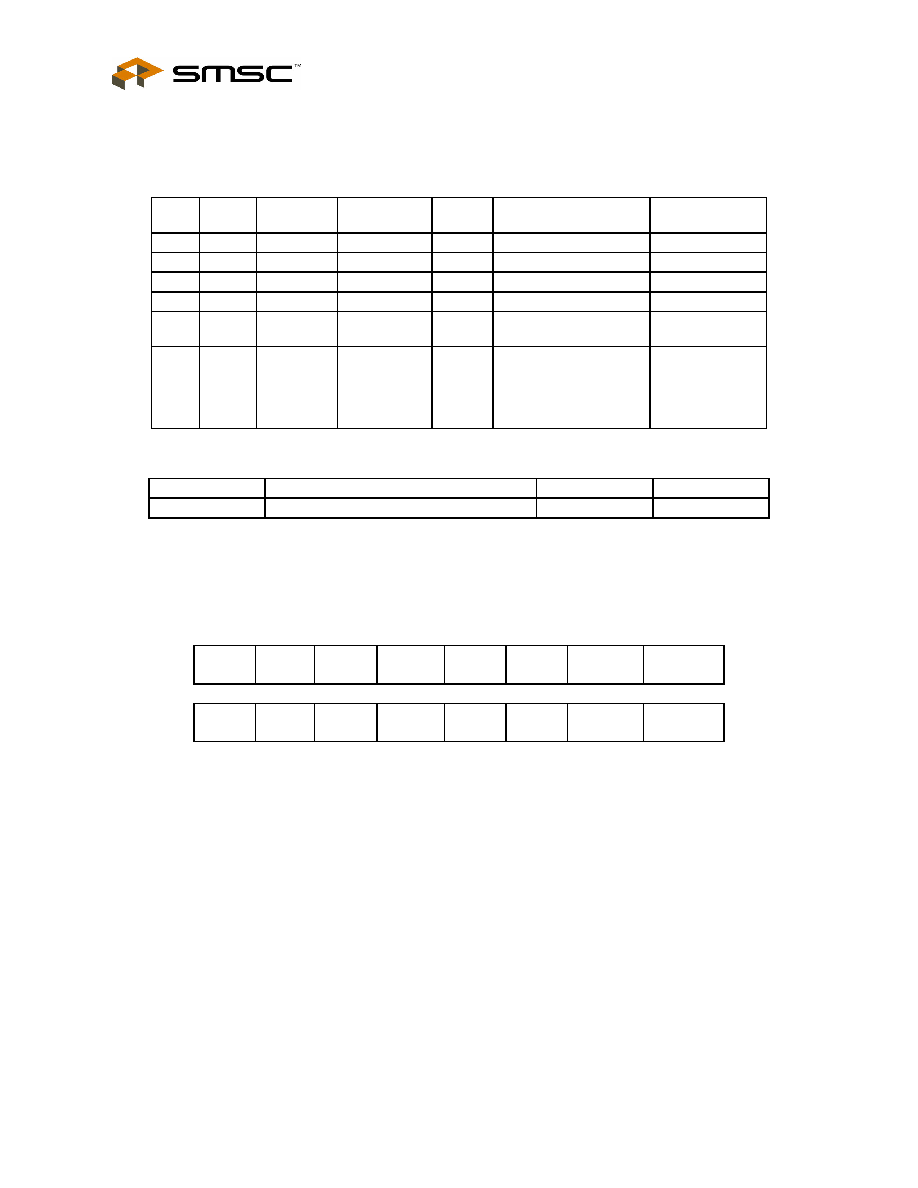
Non-PCI Single-Chip Full Duplex Ethernet Controller with Magic Packet
Rev. 09/10/2004
Page 44
SMSC LAN91C965v&3v
DATASHEET
TXENA - Transmit enabled when set. Transmit is disabled if clear. When the bit is cleared the LAN91C96
will complete the current transmission before stopping. When stopping due to an error, this bit is
automatically cleared.
Table 7.1 - Transmit Loop
AUI FDSE FDUPLX EPH_LOOP LOOP
LOOPS
AT
TRANSMITS
TO NETWORK
X
X
X
1
X
EPH Block
No
X
X
1
0
1
ENDEC
No
1
0
1
0
0
Cable
Yes
0
0
1
0
0
10BASE-T Driver
Yes
X
0
0
0
0
NORMAL CSMA/CD -
No Loopback
Yes
X
1
1
0
0
FULL DUPLEX
SWITCHED
ETHERNET - No
loopback and No
SQET
Yes
I/O SPACE - BANK0
OFFSET NAME TYPE
SYMBOL
2
EPH STATUS REGISTER
READ ONLY
EPHSR
This register stores the status of the last transmitted frame. This register value, upon individual transmit
packet completion, is stored as the first word in the memory area allocated to the packet. Packet interrupt
processing should use the copy in memory as the register itself will be updated by subsequent packet
transmissions. The register can be used for real time values (like TXENA and LINK OK). If TXENA is
cleared the register holds the last packet completion status.
TX
UNRN
LINK_
OK
RES
CTR
_ROL
EXC
_DEF
LOST
CARR
LATCOL WAKEUP
0 0 0 0 0 0 0
0
TX
DEFR
LTX
BRD
SQET 16COL
LTX
MULT
MUL
COL
SNGL
COL
TX_SUC
0 0 0 0 0 0 0
0
TXUNRN - Transmit Under run. Set if Under run occurs, it also clears TXENA bit in TCR. Cleared by
setting TXENA high. This bit should never be set under normal operation.
LINK_OK - State of the 10BASE-T Link Integrity Test. A transition on the value of this bit generates an
interrupt when the LE ENABLE bit in the Control Register is set.
RES ≠ This bit is reserved and will always return a zero(0).
CTR_ROL - Counter Roll over. When set one or more 4 bit counters have reached maximum count (15).
Cleared by reading the ECR register.
EXC_DEF - Excessive deferral. When set last/current transmit was deferred for more than 1518 * 2 byte
times. Cleared at the end of every packet sent.

Non-PCI Single-Chip Full Duplex Ethernet Controller with Magic Packet
SMSC LAN91C965v&3v
Page 45
Rev. 09/10/2004
DATASHEET
LOST_CARR - Lost carrier sense. When set indicates that Carrier Sense was not present at end of
preamble. Valid only if MON_CSN is enabled. This condition causes TXENA bit in TCR to be reset.
Cleared by setting TXENA bit in TCR.
LATCOL - Late collision detected on last transmit frame. If set a late collision was detected (later than 64
byte times into the frame). When detected the transmitter JAMs and turns itself off clearing the TXENA bit
in TCR. Cleared by setting TXENA in TCR.
WAKEUP - When this bit is set, it indicates that a receive packet was received that had the "Magic" packet
(MP) signature of the node's own Individual address repetitions in it. This bit indicates a valid detection for
magic packet.
TX_DEFR - Transmit Deferred. When set, carrier was detected during the first 6.4 uSec of the inter frame
gap. Cleared at the end of every packet sent.
LTX_BRD - Last transmit frame was a broadcast. Set if frame was broadcast. Cleared at the start of every
transmit frame.
SQET - Signal Quality Error Test. The transmitter opens a 1.6 us window 0.8 us after transmission is
completed and the receiver returns inactive. During this window, the transmitter expects to see the SQET
signal from the transceiver. The absence of this signal is a 'Signal Quality Error' and is reported in this
status bit. Transmission stops and EPH INT is set if STP_SQET is in the TCR is also set when SQET is
set. This bit is cleared by setting TXENA high.
16COL - 16 collisions reached. Set when 16 collisions are detected for a transmit frame. TXENA bit in TCR
is reset. Cleared when TXENA is set high.
LTX_MULT - Last transmit frame was a multicast. Set if frame was a multicast. Cleared at the start of
every transmit frame.
MULCOL - Multiple collision detected for the last transmit frame. Set when more than one collision was
experienced. Cleared when TX_SUC is high at the end of the packet being sent.
SNGLCOL - Single collision detected for the last transmit frame. Set when a collision is detected. Cleared
when TX_SUC is high at the end of the packet being sent.
TX_SUC - Last transmit was successful. Set if transmit completes without a fatal error. This bit is cleared
by the start of a new frame transmission or when TXENA is set high.
Fatal errors are:
16
collisions
SQET fail and STP_SQET = 1
FIFO
Underrun
Carrier lost and MON_CSN = 1
Late
collision
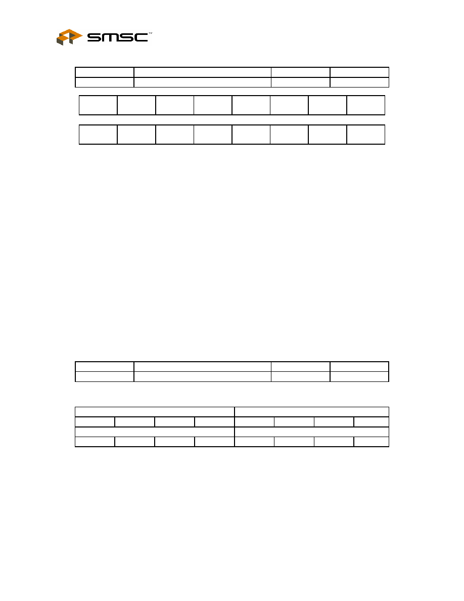
Non-PCI Single-Chip Full Duplex Ethernet Controller with Magic Packet
Rev. 09/10/2004
Page 46
SMSC LAN91C965v&3v
DATASHEET
I/O SPACE - BANK0
OFFSET NAME TYPE
SYMBOL
4
RECEIVE CONTROL REGISTER
READ/WRITE
RCR
SOFT
RST
FILT
CAR
0 0 0 0
STRIP
CRC
RXEN
0 0 0 0 0 0 0 0
ALMUL
PRMS
RX_
ABORT
0 0 0 0 0 0 0 0
SOFT_RST - Software activated Reset. Active high. Initiated by writing this bit high and terminated by
writing the bit low. The LAN91C96 configuration is not preserved, except for Configuration, Base, and IA0-
5 Registers. The EEPROM in both LOCAL BUS and PCMCIA mode is not reloaded after software reset.
FILT_CAR - Filter Carrier. When set filters leading edge of carrier sense for 12 bit times. Otherwise
recognizes a receive frame as soon as carrier sense is active.
STRIP_CRC - When set it strips the CRC on received frames. When clear the CRC is stored in memory
following the packet. Defaults low.
RXEN - Enables the receiver when set. If cleared, completes receiving current frame and then goes idle.
Defaults low on reset.
ALMUL - When set accepts all multicast frames (frames in which the first bit of DA is '1'). When clear
accepts only the multicast frames that match the multicast table setting. Defaults low.
PRMS - Promiscuous mode. When set receives all frames.
Change vs. LAN91C92: Does not receive its own transmission when not in full duplex(FDUPLX)!.
RX_ABORT - This bit is set if a receive frame was aborted due to length longer than 1532 bytes. The
frame will not be received. The bit is cleared by RESET or by the CPU writing it low.
I/O SPACE - BANK0
OFFSET NAME TYPE
SYMBOL
6
COUNTER REGISTER
READ ONLY
ECR
Counts four parameters for MAC statistics. When any counter reaches 15 an interrupt is issued. All
counters are cleared when reading the register, and do not wrap around beyond 15.
NUMBER OF EXC. DEFERRED TX
NUMBER OF DEFERRED TX
0 0 0 0 0 0 0 0
MULTIPLE COLLISION COUNT
SINGLE COLLISION COUNT
0 0 0 0 0 0 0 0
Each four bit counter is incremented every time the corresponding event, as defined in the EPH STATUS
REGISTER bit description, occurs. Note that the counters can only increment once per enqueued transmit
packet, never faster, limiting the rate of interrupts that can be generated by the counters. For example if a
packet is successfully transmitted after one collision the SINGLE COLLISION COUNT field is incremented
by one. If a packet experiences between 2 to 16 collisions, the MULTIPLE COLLISION COUNT field is
incremented by one.
If a packet experiences deferral the NUMBER OF DEFERRED TX field is incremented by one, even if the
packet experienced multiple deferrals during its collision retries.
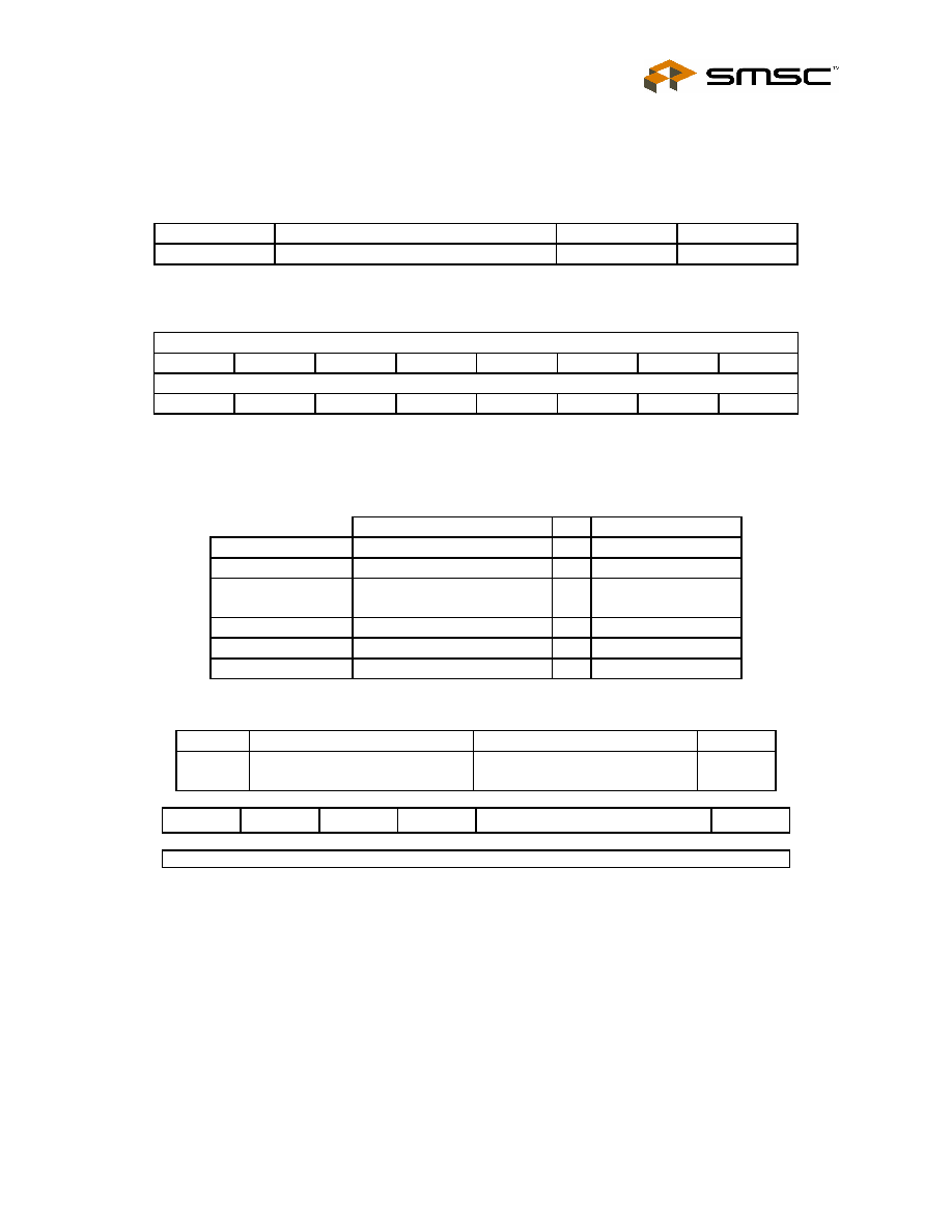
Non-PCI Single-Chip Full Duplex Ethernet Controller with Magic Packet
SMSC LAN91C965v&3v
Page 47
Rev. 09/10/2004
DATASHEET
The COUNTER REGISTER facilitates maintaining statistics in the AUTO RELEASE mode where no
transmit interrupts are generated on successful transmissions.
Reading the register in the transmit service routine will be enough to maintain statistics.
I/O SPACE - BANK0
OFFSET NAME TYPE
SYMBOL
8
MEMORY INFORMATION REGISTER
READ ONLY
MIR
For software compatibility with other LAN9000 parts all memory-related information is represented in 256 x
M byte units, where the multiplier M is determined by the MCR upper byte. M equals "1" for the
LAN91C96.
FREE MEMORY AVAILABLE (in BYTES* 256* M)
0 0 0 1 1 0 0 0
MEMORY SIZE (in BYTES* 256* M)
0 0 0 1 1 0 0 0
FREE MEMORY AVAILABLE - This register can be read at any time to determine the amount of free
memory. The register defaults to the MEMORY SIZE upon reset or upon the RESET MMU command.
MEMORY SIZE - This register can be read to determine the total memory size, and will always read 18H
(6144 bytes) for the LAN91C96.
MEMORY SIZE REGISTER
M
ACTUAL MEMORY
LAN91C90 FFH
1
64
kbytes
LAN91C90 40H
1
16
kbytes
LAN91C92/
LAN91C94
12H 1
4608
bytes
LAN91C95 18H
1
6144
bytes
LAN91C96 18H
1
6144
bytes
LAN91C100 FFH
2
128
kbytes
I/O SPACE - BANK0
OFFSET NAME
TYPE SYMBOL
A
MEMORY CONFIGURATION
REGISTER
LOWER BYTE READ/WRITE
UPPER BYTE READ ONLY
MCR
Memory
Size
Multiplier
"M"
0 0 1 1 0 0 1 1
Memory Reserved for Transmit (in BYTES * 256 * M)
0 0 0 0 0 0 0 0
MEMORY RESERVED FOR TRANSMIT -
Programming this value allows the host CPU to reserve memory to be used later for transmit, limiting the
amount of memory that receive packets can use up. When programmed for zero, the memory allocation
between transmit and receive is completely dynamic. When programmed for a non-zero value, the
allocation is dynamic if the free memory exceeds the programmed value, while receive allocation requests
are denied if the free memory is less or equal to the programmed value. This register defaults to zero
upon reset. It is not affected by the RESET MMU command.
The value written to the MCR is a reserved memory space IN ADDITION TO ANY MEMORY
CURRENTLY IN USE. If the memory allocated for transmit plus the reserved space for transmit is required
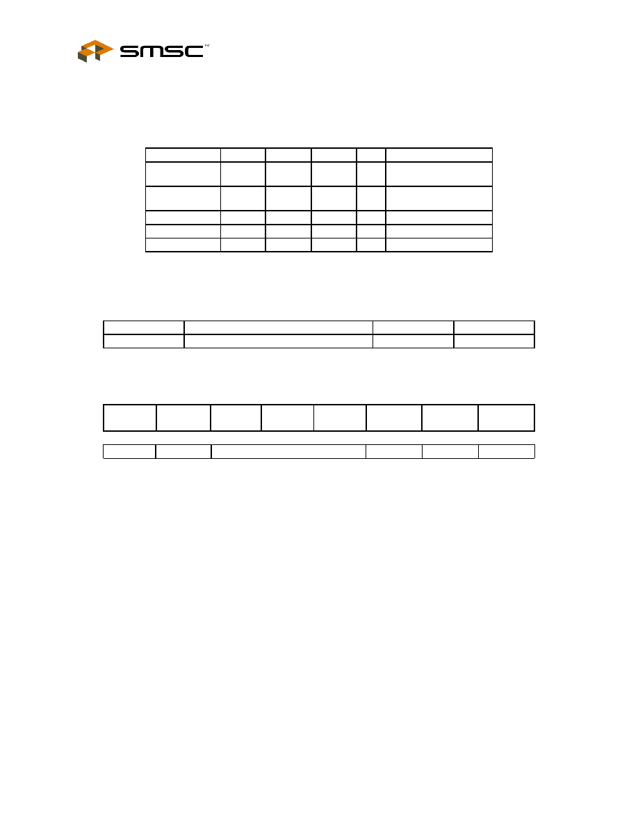
Non-PCI Single-Chip Full Duplex Ethernet Controller with Magic Packet
Rev. 09/10/2004
Page 48
SMSC LAN91C965v&3v
DATASHEET
to be constant (rather than grow with transmit allocations) the CPU should update the value of this register
after allocating or releasing memory.
The contents of MIR as well as the low byte of MCR are specified in 256* M bytes. The multiplier M is
determined by bits 11, 10 and 9 as follows:
DEVICE
BIT 11
BIT 10
BIT 9
M
MAX MEMORY SIZE
FEAST 0 1 0
2
256
(Note 7.1)
256
(Note 7.1)
2=128k
LAN91C90 0 0 1 1
256
(Note 7.1)
256
(Note 7.1)
1=64k
FUTURE 0 1 1
4
256k
FUTURE 1 0 0
8
512k
FUTURE 1 0 1
16
1M
Note 7.1
Bits 11, 10 and 9 are read only bits used by the software driver to transparently run on different controllers of
the LAN9000 family.
I/O SPACE - BANK1
OFFSET NAME TYPE
SYMBOL
0 CONFIGURATION
REGISTER
READ/WRITE
CR
The Configuration Register holds bits that define the device configuration and are not expected to change
during run-time. This register is part of the EEPROM saved setup in LOCAL BUS mode only. In PCMCIA
mode, this register is initialized to the state as defined below as if not EEPROM is present in LOCAL BUS
mode (ie. ENEEP Pin is a don't care in PCMCIA mode)
0
NO
WAIT
FULL
STEP
SET
SQLCH
AUI
SELECT
0 X X 0 X 0 0 0
16BIT
DIS LINK
Reserved
INT SEL1
INT SEL0
function
of EN16*
pin
0
1
1
0
0
0
X
NO WAIT - When set, does not request additional wait states. An exception to this are accesses
to the Data Register if not ready for a transfer. When clear, negates IOCHRDY for two to three
20MHz clocks on any cycle to the LAN91C96.
FULL STEP - This bit is used to select the signaling mode for the AUI port. When set the AUI port
uses full step signaling. Defaults low to half step signaling. This bit is only meaningful when AUI
SELECT is high.
SET SQLCH - When set, the squelch level used for the 10BASE-T receive signal is 240mV.
When clear the receive squelch level is 400mV. Defaults low.
AUI SELECT - When set the AUI interface is used, when clear the 10BASE-T interface is used.
Defaults low.
16BIT - Used in conjunction with EN16* and IO is 8 to define the width of the system bus. If the
EN16* pin is low, this bit is forced high. Otherwise the bit defaults low and can be programmed by
the host CPU.
Non-PCI Single-Chip Full Duplex Ethernet Controller with Magic Packet
SMSC LAN91C965v&3v
Page 49
Rev. 09/10/2004
DATASHEET
DIS LINK - This bit is used to disable the 10BASE-T link test functions. When this bit is high the
LAN91C96 disables link test functions by not generating nor monitoring the network for link
pulses. In this mode the LAN91C96 will transmit packets regardless of the link test, the EPHSR
LINK_OK bit will be set and the LINK LED will stay on. When low the link test functions are
enabled. If the link status indicates FAIL, the EPHSR LINK_OK bit will be low, while transmit
packets enqueued will be processed by the LAN91C96, transmit data will not be sent out to the
cable.
INT SEL1-0 - In LOCAL BUS mode, used to select one out of four interrupt pins. The three
unused interrupts are tristated.
INT SEL1
INT SEL0
INTERRUPT PIN USED
0
0
INTR0
0
1
INTR1
1
0
INTR2
1
1
INTR3
I/O SPACE - BANK1
OFFSET NAME
TYPE
SYMBOL
2 BASE
ADDRESS
REGISTER
READ/WRITE
BAR
For LOCAL BUS mode only, this register holds the I/O address decode option chosen for the I/O and ROM
space. It is part of the EEPROM saved setup, and is not usually modified during run-time.
A15 A14 A13 A9 A8 A7 A6 A5
0 0 0 1 1 0 0 0
ROM
SIZE
RA18 RA17 RA16 RA15 RA14
0 1 1 0 0 1 1 1
A15 - A13 and A9 - A5 - These bits are compared in LOCAL BUS mode against the I/O address on the
bus to determine the IOBASE for LAN91C96 registers. The 64k I/O space is fully decoded by the
LAN91C96 down to a 16 location space, therefore the unspecified address lines A4, A10, A11 and A12
must be all zeros.
ROM SIZE - Determines the ROM decode area in LOCAL BUS mode memory space as follows:
00 = ROM disable
01 = 16k: RA14-18 define ROM select.
10 = 32k: RA15-18 define ROM select.
11 = 64k: RA16-18 define ROM select.
RA18-RA14 - These bits are compared in LOCAL BUS mode against the memory address on the bus to
determine if the ROM is being accessed, as a function of the ROM SIZE. ROM accesses are read only
memory accesses defined by MEMRD* going low.
For a full decode of the address space unspecified upper address lines have to be: A19 = "1", A20-A23
lines are not directly decoded, however LOCAL BUS systems will only activate SMEMRD* only when A20-
A23=0.
All bits in this register are loaded from the serial EEPROM in LOCAL BUS Mode only. In PCMCIA mode,
the I/O base is set to the default value (as in LOCAL BUS mode) as defined below.

Non-PCI Single-Chip Full Duplex Ethernet Controller with Magic Packet
Rev. 09/10/2004
Page 50
SMSC LAN91C965v&3v
DATASHEET
The I/O base decode defaults to 300h (namely, the high byte defaults to 18h). ROM SIZE defaults to 01.
ROM decode defaults to CC000 (namely the low byte defaults to 67h).
Below chart shows the decoding of I/O Base Address 300h:
A15
A14
A13
A12
A11
A10 A9
A8
A7
A6
A5
A4
A3
A2
A1
A0
0
0
0
0
0
0
1
1
0
0
0
0
0
0
0
0
I/O SPACE - BANK1
OFFSET NAME TYPE
SYMBOL
4 THROUGH 9
INDIVIDUAL ADDRESS REGISTERS
READ/WRITE
IAR
These registers are loaded starting at word location 20h of the EEPROM upon hardware reset or
EEPROM reload. The registers can be modified by the software driver, but a STORE operation will not
modify the EEPROM Individual Address contents.
Bit 0 of Individual Address 0 register corresponds to the first bit of the address on the cable.
ADDRESS 0
0 0 0 0 0 0 0
0
ADDRESS 1
0 0 0 0 0 0 0
0
ADDRESS 2
0 0 0 0 0 0 0
0
ADDRESS 3
0 0 0 0 0 0 0
0
ADDRESS 4
0 0 0 0 0 0 0
0
ADDRESS 5
0 0 0 0 0 0 0
0
Non-PCI Single-Chip Full Duplex Ethernet Controller with Magic Packet
SMSC LAN91C965v&3v
Page 51
Rev. 09/10/2004
DATASHEET
I/O SPACE - BANK1
OFFSET NAME TYPE
SYMBOL
A GENERAL
ADDRESS
REGISTERS
READ/WRITE
GPR
HIGH DATA BYTE
0 0 0 0 0 0 0 0
LOW DATA BYTE
0 0 0 0 0 0 0 0
This register can be used as a way of storing and retrieving non-volatile information in the EEPROM to be
used by the software driver. The storage is word oriented, and the EEPROM word address to be read or
written is specified using the six lowest bits of the Pointer Register.
This register can also be used to sequentially program the Individual Address area of the EEPROM, that is
normally protected from accidental Store operations.
This register will be used for EEPROM read and write only when the EEPROM SELECT bit in the Control
Register is set. This allows generic EEPROM read and write routines that do not affect the basic setup of
the LAN91C96.
I/O SPACE - BANK1
OFFSET NAME TYPE
SYMBOL
C CONTROL
REGISTER
READ/WRITE
CTR
0 RCV_
BAD
PWRDN
WAKEUP
_EN
AUTO
RELEAS
E
1
0 0 0 0 0 X X 1
LE
ENABLE
CR
ENABLE
TE
ENABLE
EEPROM
SELECT
RELOAD STORE
0 0 0 X X 0 0 0
RCV_BAD - When set, bad CRC packets are received. When clear bad CRC packets do not generate
interrupts and their memory is released.
PWRDN - Active high bit used to put the Ethernet function in power down mode.
Cleared by:
1. A write to any register in the LAN91C96 I/O space.
2. Hardware reset. This bit is combined with the Pwrdwn bit in ECSR and with the powerdown bit to
determine when the function is powered down.
WAKUP_EN - Active high bit used to enable the controller in the appropriate power down modes to power
up and set the WAKEUP bit in the EPHSR -> generate an EPH interrupt(if not masked). When clear (0),
no "Magic Packet" scanning is done on receive packets.
Note:
Setting (1) the bit is meaningful only if the function is enabled (Enable Function bit in COR; offset 8000h)

Non-PCI Single-Chip Full Duplex Ethernet Controller with Magic Packet
Rev. 09/10/2004
Page 52
SMSC LAN91C965v&3v
DATASHEET
AUTO RELEASE - When set, transmit pages are released by transmit completion if the transmission was
successful (when TX_SUC is set). In that case there is no status word associated with its packet number,
and successful packet numbers are not even written into the TX COMPLETION FIFO.
A sequence of transmit packets will only generate an interrupt when the sequence is completely
transmitted (TX EMPTY INT will be set), or when a packet in the sequence experiences a fatal error (TX
INT will be set). Upon a fatal error TXENA is cleared and the transmission sequence stops. The packet
number that failed is the present in the FIFO PORTS register, and its pages are not released, allowing the
CPU to restart the sequence after corrective action is taken.
LE ENABLE - Link Error Enable. When set it enables the LINK_OK bit transition as one of the interrupts
merged into the EPH INT bit. Defaults low (disabled). Writing this bit also serves as the acknowledge by
clearing previous LINK interrupt conditions.
CR ENABLE - Counter Roll over Enable. When set it enables the CTR_ROL bit as one of the interrupts
merged into the EPH INT bit. Defaults low (disabled).
TE ENABLE - Transmit Error Enable. When set it enables Transmit Error as one of the interrupts merged
into the EPH INT bit. Defaults low (disabled). Transmit Error is any condition that clears TXENA with
TX_SUC staying low as described in the EPHSR register.
EEPROM SELECT - This bit allows the CPU to specify which registers the EEPROM RELOAD or STORE
refers to.
When high, the General Purpose Register is the only register read or written. When low, the RELOAD and
STORE functions are enabled.
RELOAD
The LAN91C96 reads the Configuration, Base and Individual Address, and STORE writes the
Configuration and Base registers.
Also when set it will read the EEPROM and update relevant registers with its contents. This bit then Clears
upon completing the operation.
STORE
The STORE LAN91C96 bit when set, stores the contents of all relevant registers in the serial EEPROM.
This bit is cleared upon completing the operation.
Note:
When an EEPROM access is in progress the STORE and RELOAD bits will be read back as high. The
remaining 14 bits of this register will be invalid. During this time, attempted read/write operations, other
than polling the EEPROM status, will NOT have any effect on the internal registers. The CPU can resume
accesses to the LAN91C96 after both bits are low. A worst case RELOAD operation initiated by RESET or
by software takes less than 750usec in either mode.
Non-PCI Single-Chip Full Duplex Ethernet Controller with Magic Packet
SMSC LAN91C965v&3v
Page 53
Rev. 09/10/2004
DATASHEET
I/O SPACE - BANK2
OFFSET NAME
TYPE
SYMBOL
0
MMU COMMAND REGISTER
WRITE ONLY
BUSY bit readable
MMUCR
This register is used by the CPU to control the memory allocation, de-allocation, TX FIFO and RX FIFO
control. The three command bits determine the command issued as described below:
COMMAND
0
N2
N1
N0/
BUSY
w
x
y
z
0
COMMAND SET:
wxyz
0000
0)
NOOP - NO OPERATION -
0010
2)
ALLOCATE MEMORY FOR TX - N2, N1, N0 defines the amount of memory
requested as (value + 1) 256* bytes. Namely N2, N1, N0 = 1 will request 2
256* = 512 bytes. Valid range for N2, N1, N0 is 0 through 5. A shift-based divide
by 256 of the packet length yields the appropriate value to be used as N2, N1
and N0. Immediately generates a completion code at the ALLOCATION RESULT
REGISTER. Can optionally generate an interrupt on successful completion. The
allocation time can take worst case (N2, N1, N0 + 2)* 200ns.
0100
4)
RESET MMU TO INITIAL STATE - Frees all memory allocations, clears relevant
interrupts, resets packet FIFO pointers.
0110
6)
REMOVE FRAME FROM TOP OF RX FIFO- To be issued after CPU has
completed processing of present receive frame. This command removes the
receive packet number from the RX FIFO and brings the next receive frame (if
any) to the RX area (output of RX FIFO).
0111
7)
REMOVE FRAME FROM TOP OF TX FIFO- To be issued ONLY after the Host
disabled the transmitter and has completed processing of the present transmit
frame. Note: Determining Transmit completion is done by polling the TEMPTY bit
in the Transmit FIFO Port Register. This command removes the Transmit packet
number from the TX FIFO and brings the next Transmit frame (if any) to the TX
area (output of TX FIFO).
8)
REMOVE AND RELEASE TOP OF RX FIFO - Like 6) but also releases all
memory used by the packet presently at the RX FIFO output.
1010
A)
RELEASE SPECIFIC PACKET - Frees all pages allocated to the packet
specified in the PACKET NUMBER REGISTER. Should not be used for frames
pending transmission. Typically used to remove transmitted frames, after reading
their completion status.
Can be used following 6 (to release receive packet memory in a more flexible way than 8).
1100
C)
ENQUEUE PACKET NUMBER INTO TX FIFO - This is the normal method of
transmitting a packet just loaded into RAM. The packet number to be enqueued
is taken from the PACKET NUMBER REGISTER.
Non-PCI Single-Chip Full Duplex Ethernet Controller with Magic Packet
Rev. 09/10/2004
Page 54
SMSC LAN91C965v&3v
DATASHEET
1110
F)
RESET TX FIFOs - This command will reset both TX FIFOs. The TX FIFO
holding the packet numbers awaiting transmission and the TX Completion FIFO.
This command provides a mechanism for canceling packet transmissions, and
reordering or bypassing the transmit queue.
The RESET TX FIFOs command should only be used when the transmitter is disabled. Unlike the RESET
MMU command, the RESET TX FIFOs does not release any memory.
Notes:
Only command 2 uses N2, N1 and N0.
When using the RESET TX FIFOS command, the CPU is responsible for releasing the memory associated with
outstanding packets, or re-enqueuing them. Packet numbers in the completion FIFO can be read via the FIFO
ports register before issuing the command.
MMU commands releasing memory (commands 8 and A) should only be issued if the corresponding packet
number has memory allocated to it.
COMMAND SEQUENCING
A second allocate command (command 2) should not be issued until the present one has completed.
Completion is determined by reading the FAILED bit of the allocation result register or through the
allocation interrupt. A second release command (commands 8 and A) should not be issued if the previous
one is still being processed. The BUSY bit indicates that a release command is in progress. After issuing
command A, the contents of the PNR should not be changed until BUSY goes low. After issuing command
8, command 6 should not be issued until BUSY goes low. BUSY BIT - Readable at bit "0" of the MMU
command register address. When set indicates that MMU is still processing a release command. When
clear, MMU has already completed last release command. BUSY and FAILED bits are set upon the
trailing edge of command.
I/O SPACE - BANK2
OFFSET NAME TYPE
SYMBOL
1
AUTO TX START REGISTER
READ/WRITE
AUTOTX
D7 D6 D5 D4 D3 D2 D1 D0
0 0 0 0 0 0 0 0
AUTO TX START REGISTER - This register specifies the value, in 16 byte multiples of when the transmit
state machine starts a transmit operation when the associated transmit buffer is enqueued into the
transmit FIFO.
The AutoTx bit as well as the ETEN bit must both be set in the pointer register in order for this register to
be utilized. Note: This register must be non-zero for the Auto-Tx function to work. A value of "0" will disable
this function. The RCV bit in the Pointer register must be zero (0) as well. The RCV bit must be cleared so
that the packet being written and enqueued is being selected by the PNR and not the receive FIFO.
Register Operation: When Early Transmit is enabled via the ETEN bit in the pointer register, the host is
able to enqueue a buffer for transmit operation before all of the transmitted data is copied into the
LAN91C96 dual ported RAM. In the case of the AutoTx bit being cleared, the host must manually start the
transmit operation. When the AutoTx bit is set, the EPH Transmit engine compares the number of bytes
moved into the transmit packet buffer with the value of the Auto TX Start Register to start transmit
operation. This eliminates the requirement for the host to manually start the transmit.
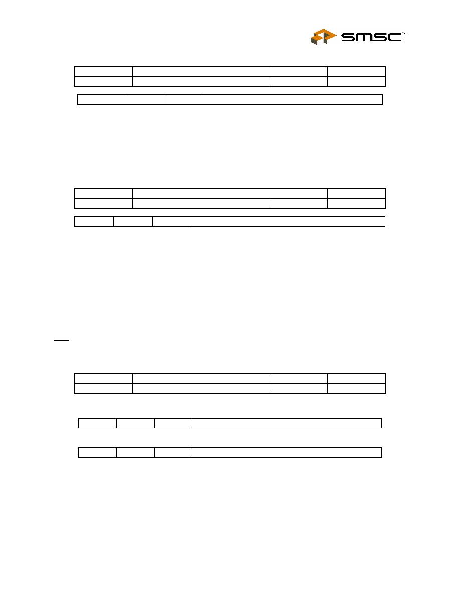
Non-PCI Single-Chip Full Duplex Ethernet Controller with Magic Packet
SMSC LAN91C965v&3v
Page 55
Rev. 09/10/2004
DATASHEET
I/O SPACE - BANK2
OFFSET NAME TYPE
SYMBOL
2
PACKET NUMBER REGISTER
READ/WRITE
PNR
RESERVED
PACKET NUMBER AT TX AREA
0
0 0 0 0 0 0 0
PACKET NUMBER AT TX AREA - The value written into this register determines which packet number is
accessible through the TX area. Some MMU commands use the number stored in this register as the
packet number parameter. This register is cleared by a RESET or a RESET MMU Command.
RESERVED ≠ This bit is reserved.
I/O SPACE - BANK2
OFFSET NAME TYPE
SYMBOL
3
ALLOCATION RESULT REGISTER
READ ONLY
ARR
FAILED
ALLOCATED PACKET NUMBER
1 0 0 0 0 0 0 0
FAILED - A "0" indicates a successful allocation completion. If the allocation fails the bit is set and only
cleared when the pending allocation is satisfied. Defaults high upon reset and reset MMU command. For
polling purposes, the ALLOC_INT in the Interrupt Status Register should be used because it is
synchronized to the read operation. Sequence:
1. Allocate
Command
2. Poll ALLOC_INT bit until set
3. Read Allocation Result Register
ALLOCATED PACKET NUMBER - Packet number associated with the last memory allocation request.
The value is only valid if the FAILED bit is clear.
Note:
For software compatibility with future versions, the value read from the ARR after an allocation request is
intended to be written into the PNR as is, without masking higher bits (provided FAILED = "0").
I/O SPACE - BANK2
OFFSET NAME TYPE
SYMBOL
4
FIFO PORTS REGISTER
READ ONLY
FIFO
This register provides access to the read ports of the Receive FIFO and the Transmit completion FIFO.
The packet numbers to be processed by the interrupt service routines are read from this register.
REMPTY
RX FIFO PACKET NUMBER
1 0 0 0 0 0 0 0
TEMPTY
TX FIFO PACKET NUMBER
1 0 0 0 0 0 0 0
REMPTY - No receive packets queued in the RX FIFO. For polling purposes, uses the RCV_INT bit in the
Interrupt Status Register.
TOP OF RX FIFO PACKET NUMBER - Packet number presently at the output of the RX FIFO. Only valid
if REMPTY is clear. The packet is removed from the RX FIFO using MMU Commands 6) or 8).
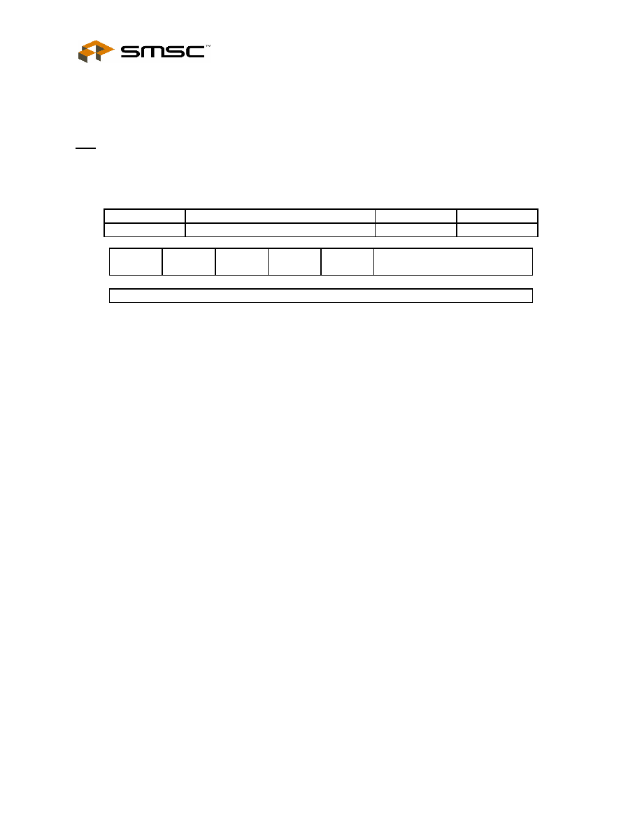
Non-PCI Single-Chip Full Duplex Ethernet Controller with Magic Packet
Rev. 09/10/2004
Page 56
SMSC LAN91C965v&3v
DATASHEET
TEMPTY - No transmit packets in completion queue. For polling purposes, uses the TX_INT bit in the
Interrupt Status Register.
TX FIFO PACKET NUMBER - Packet number presently at the output of the TX FIFO. Only valid if
TEMPTY is clear. The packet is removed when a TX INT acknowledge is issued.
Note:
For software compatibility with future versions, the value read from each FIFO register is intended to be written
into the PNR as is, without masking higher bits (provided TEMPTY and REMPTY = 0 respectively).
I/O SPACE - BANK2
OFFSET NAME TYPE
SYMBOL
6 POINTER
REGISTER
READ/WRITE
PTR
RCV
AUTO
INCR.
READ ETEN AutoTx
POINTER HIGH
0 0 0 0 0 0 0 0
POINTER LOW
0 0 0 0 0 0 0 0
POINTER REGISTER - The value of this register determines the address to be accessed within the
transmit or receive areas. It will auto-increment on accesses to the data register when AUTO INCR. is set.
The increment is by one for every byte access, and by two for every word access. When RCV is set the
address refers to the receive area and uses the output of RX FIFO as the packet number, when RCV is
clear the address refers to the transmit area and uses the packet number at the Packet Number Register.
READ bit - Determines the type of access to follow. If the READ bit is high the operation intended is a
read. If the READ bit is low the operation is a write. Loading a new pointer value, with the READ bit high,
generates a pre-fetch into the Data Register for read purposes.
Read-back of the pointer will indicate the value of the address last accessed by the CPU (rather than the
last pre-fetched). This allows any interrupt routine that uses the pointer, to save it and restore it without
affecting the process being interrupted.
The Pointer Register should not be loaded until 400ns after the last write operation to the Data Register to
ensure that the Data Register FIFO is empty. On reads, if IOCHRDY is not connected to the host, the Data
Register should not be read before 400ns after the pointer was loaded to allow the Data Register FIFO to
fill.
If the pointer is loaded using 8 bit writes, the low byte should be loaded first and the high byte last.
ETEN bit - When set enables EARLY Transmit underrun detection. Normal operation when clear.
If TCR bit 14 (ETEN-TYPE) is zero and this bit is set, the Early transmit underrun function will be enabled
as it was implemented in the LAN91C94:
"The Early Transmit function allows the CPU to enqueue the first transmit packet before it is fully loaded in
packet memory. The loading operation proceeds in parallel with the transmission, and in the case that the
transmitter gets ahead of the CPU, the LAN91C94 will prevent the transmission of erroneous data by
forcing an Underrun condition. Underruns will be triggered by starving the transmit DMA if the LAN91C96
detects that the DMA TX address exceeds the pointer address."
If TCR bit 14 (ETEN-TYPE) is zero and this bit is set, the Early transmit underrun function defined as
follows:
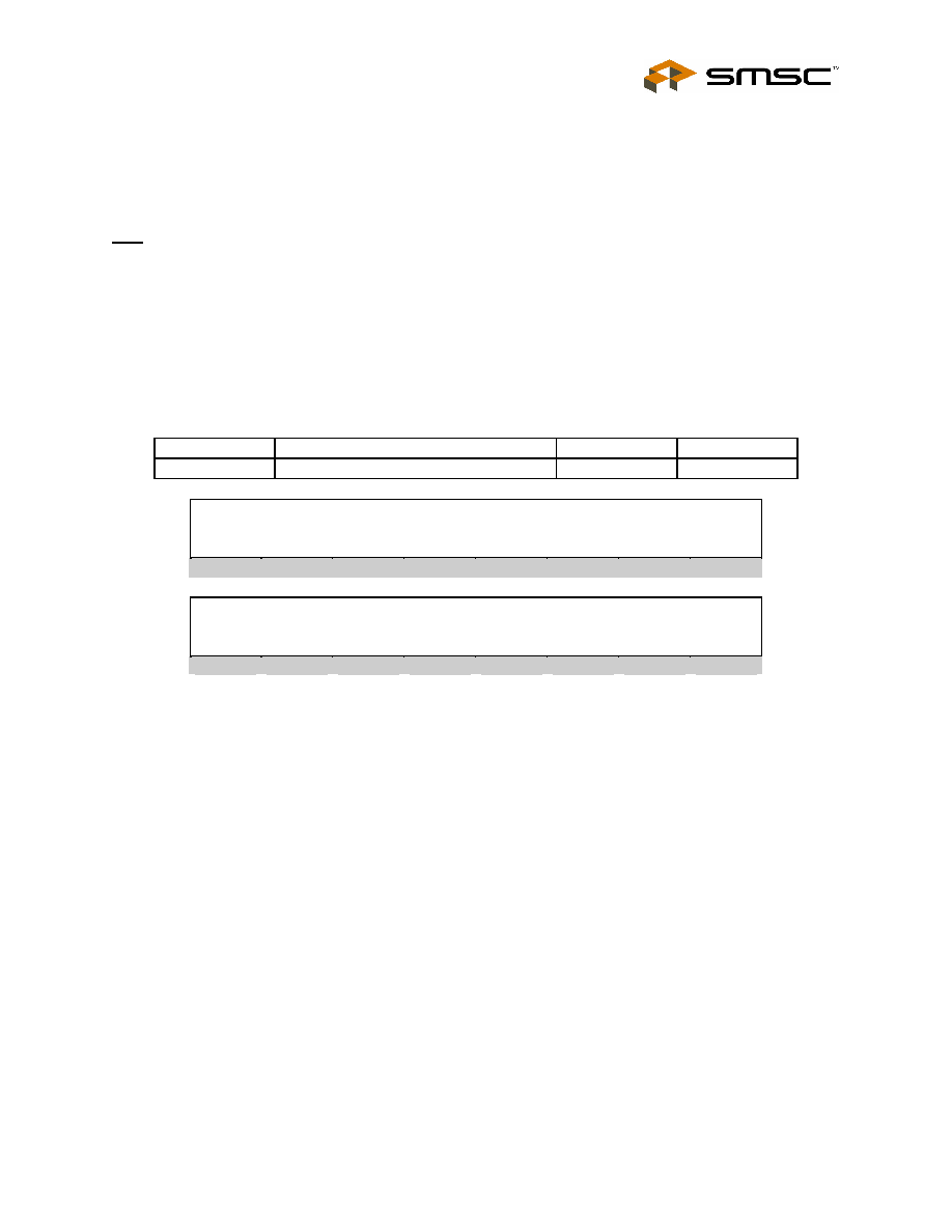
Non-PCI Single-Chip Full Duplex Ethernet Controller with Magic Packet
SMSC LAN91C965v&3v
Page 57
Rev. 09/10/2004
DATASHEET
"For underrun detection purposes the RAM logical address and packet numbers of the packet being
loaded are compared against the logical address and packet numbers of the packet being transmitted. If
the packet numbers match and the logical address of the packet being transmitted exceeds the address
being loaded the LAN91C96 will prevent the transmission of erroneous data by forcing an Underrun
condition. Underruns will be triggered by starving the transmit DMA if the LAN91C96 detects that the DMA
TX address exceeds the pointer address."
Note:
ETEN-TYPE (bit 14) in TCR may be implemented for Rev. ID 6 only. In the absence of ETEN-TYPE in
TCR, ETEN will have the definition as ETEN-TYPE were clear only.
AutoTx bit - When set, enables the transmit state machine to Automatically start a transmit operation with
no host intervention determined by the number of bytes being copied into the transmit buffer enqueued in
the transmit FIFO. The ETEN bit must also be set in order for this function to be enabled and the RCV bit
must be cleared (0). When the Auto TX bit is cleared, the transmit state machine must manually be
enabled to enqueue a transmit buffer.
If AUTO INCR. is not set, the pointer must be loaded with an even value.
I/O SPACE - BANK2
OFFSET NAME TYPE
SYMBOL
8 & A
DATA REGISTER
READ/WRITE
DATA
DATA HIGH
DATA LOW
DATA REGISTER - Used to read or write the data buffer byte/word presently addressed by the pointer
register.
This register is mapped into two uni-directional FIFOs that allow moving words to and from the LAN91C96
regardless of whether the pointer address is even or odd. Data goes through the write FIFO into memory,
and is pre-fetched from memory into the read FIFO. If byte accesses are used, the appropriate (next) byte
can be accessed through the Data Low or Data High registers. The order to and from the FIFO is
preserved. Byte and word accesses can be mixed on the fly in any order.
This register is mapped into two consecutive word locations to facilitate the usage of double word move
instructions. The DATA register is accessible at any address in the 8 through Ah range, while the number
of bytes being transferred are determined by A0 and nSBHE in LOCAL BUS mode, and by A0, nCE1 and
nCE2 in PCMCIA mode.
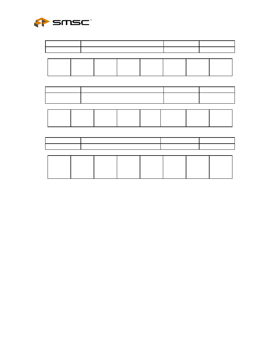
Non-PCI Single-Chip Full Duplex Ethernet Controller with Magic Packet
Rev. 09/10/2004
Page 58
SMSC LAN91C965v&3v
DATASHEET
I/O SPACE - BANK2
OFFSET NAME TYPE
SYMBOL
C
INTERRUPT STATUS REGISTER
READ ONLY
IST
TX IDLE
INT
ERCV
INT
EPH
INT
RX_
OVRN
INT
ALLOC
INT
TX
EMPTY
INT
TX INT
RCV INT
0 0 0 0 0 1 0 0
OFFSET NAME TYPE
SYMBOL
C
INTERRUPT ACKNOWLEDGE
REGISTER
WRITE ONLY
ACK
ERCV
INT
RX_
OVRN
INT
TX
EMPTY
INT
TX INT
OFFSET NAME TYPE
SYMBOL
D
INTERRUPT MASK REGISTER
READ/WRITE
MSK
TX IDLE
INT
MASK
ERCV
INT
MASK
EPH
INT
MASK
RX_
OVRN
INT
MASK
ALLOC
INT
MASK
TX
EMPTY
INT
MASK
TX INT
MASK
RCV INT
MASK
0 0 0 0 0 0 0 0
This register can be read and written as a word or as two individual bytes.
The Interrupt Mask Register bits enable the appropriate bits when high and disable them when low. A
MASK bit being set will cause a hardware interrupt.
TX IDLE INT - Transmit Idle interrupt. Set when the transmit state machine is not active. This bit is used
under the condition where the TX FIFO is still NOT empty, the transmitter is disabled and the host wants to
determine when the transmitter is completed with the current transmit packet. This event usually happens
when the host wants to insert at the head of the transmit queue a frame for example.
Typical flow of events/Condition:
1. The transmit FIFO is not empty
2. The transmit DONE FIFO is either empty or not empty
3. The transmit engine is either active or not active
Flow of events for an insertion of a transmit packet:
1. Disable the Transmitter
2. Remove and release any "transmit done" packets in the TX FIFO
3. Via polling or an interrupt driven event, determine status of TX IDLE INT bit and wait until this bit is
set. This will determine when the transmitter is truly done with all transmit events.
4. Remove and store (if any, in software) Packet numbers from the transmit FIFO. (These packets will
later be restored into the TX FIFO after the control frame is inserted into the front of the TX FIFO).
5. Enable
Transmitter

Non-PCI Single-Chip Full Duplex Ethernet Controller with Magic Packet
SMSC LAN91C965v&3v
Page 59
Rev. 09/10/2004
DATASHEET
6. En-queue
packet into TX FIFO
7. En-queue rest of packets, if any, into TX FIFO (restore TX FIFO)
ERCV INT - Early receive interrupt. Set whenever a receive packet is being received, and the number of bytes
received into memory exceeds the value programmed as ERCV THRESHOLD (Bank 3, Offset Ch). ERCV INT
stays set until acknowledged by writing the INTERRUPT ACKNOWLEDGE REGISTER with the ERCV INT bit
set.
EPH INT - Set when the Ethernet Protocol Handler section indicates one out of various possible special
conditions. This bit merges exception type of interrupt sources, whose service time is not critical to the
execution speed of the low level drivers. The exact nature of the interrupt can be obtained from the EPH Status
Register (EPHSR), and enabling of these sources can be done via the Control Register. The possible sources
are:
1. LINK - Link Test transition
2. CTR_ROL - Statistics counter roll over
3. TXENA cleared - A fatal transmit error occurred forcing TXENA to be cleared. TX_SUC will be low
and the specific reason will be reflected by the bits:
3.1
TXUNRN - Transmit under-run
3.2
SQET - SQE Error
3.3
LOST CARR - Lost Carrier
3.4
LATCOL - Late Collision
3.5
16COL - 16 collisions
Any of the above interrupt sources can be masked by the appropriate ENABLE bits in the Control Register.
1) LE ENABLE (Link Error Enable), 2) CR ENABLE (Counter Roll Over), 3) TE ENABLE (Transmit Error
Enable)
EPH INT will only be cleared by the following methods:
1. Clearing the LE ENABLE bit in the Control Register if an EPH interrupt is caused by a LINK_OK
transition.
2. Reading the Counter Register if an EPH interrupt is caused by statistics counter roll over.
3. Setting TXENA bit high if an EPH interrupt is caused by any of the fatal transmit error listed above (3.1
to 3.5).
RX_OVRN INT - Set when 1) the receiver aborts due to an overrun due to a failed memory allocation, 2)
the receiver aborts due to a packet length of greater than 2K bytes, or 3) the receiver aborts due to the
RCV DISCRD bit in the ERCV register set. The RX_OVRN INT bit latches the condition for the purpose of
being polled or generating an interrupt, and will only be cleared by writing the acknowledge register with
the RX_OVRN INT bit set.
ALLOC INT - Set when an MMU request for TX ram pages is successful. This bit is the complement of the
FAILED bit in the ALLOCATION RESULT register. The ALLOC INT bit is cleared by the MMU when the
next allocation request is processed or allocation fails.
TX EMPTY INT - Set if the TX FIFO goes empty, can be used to generate a single interrupt at the end of a
sequence of packets enqueued for transmission. This bit latches the empty condition, and the bit will stay
set until it is specifically cleared by writing the acknowledge register with the TX EMPTY INT bit set. If a
real time reading of the FIFO empty is desired, the bit should be first cleared and then read.
The TX_EMPTY MASK bit should only be set after the following steps:
a) A packet is enqueued for transmission

Non-PCI Single-Chip Full Duplex Ethernet Controller with Magic Packet
Rev. 09/10/2004
Page 60
SMSC LAN91C965v&3v
DATASHEET
b) The previous empty condition is cleared (acknowledged)
TX INT - Set when at least one packet transmission was completed or any of the below transmit fatal
errors occurs:
1. TXUNRN - Transmit under-run
2. SQET - SQE Error
3. LOST CARR - Lost Carrier
4. LATCOL - Late Collision
5. 16COL - 16 collisions
The first packet number to be serviced can be read from the FIFO PORTS register. The TX INT bit is
always the logic complement of the TEMPTY bit in the FIFO PORTS register. After servicing a packet
number, its TX INT interrupt is removed by writing the Interrupt Acknowledge Register with the TX INT bit
set.
RCV INT - Set when a receive interrupt is generated. The first packet number to be serviced can be read
from the FIFO PORTS register. The RCV INT bit is always the logic complement of the REMPTY bit in the
FIFO PORTS register.
Receive Interrupt is cleared when RX FIFO is empty.
Notes:
For edge triggered systems, the Interrupt Service Routine should clear the Interrupt Mask Register, and only
enable the appropriate interrupts after the interrupt source is serviced (acknowledged).
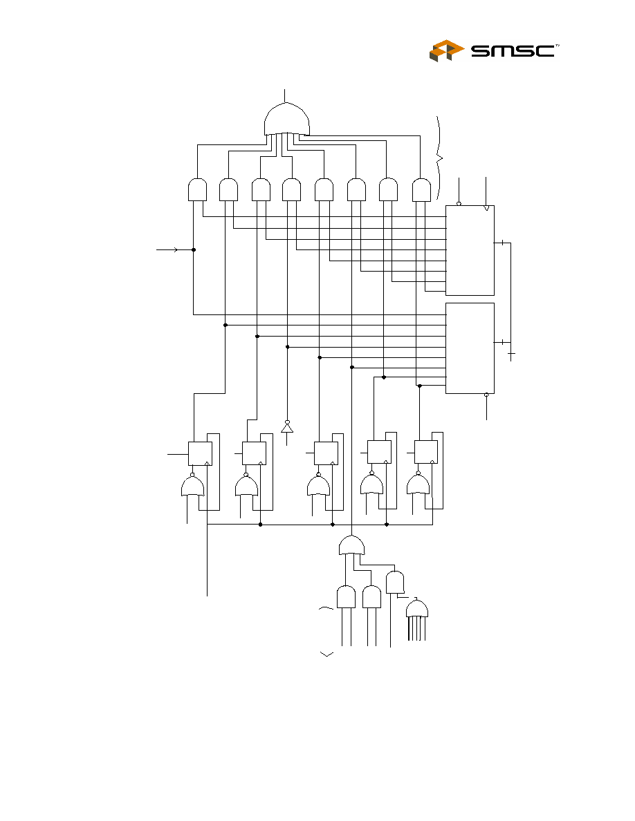
Non-PCI Single-Chip Full Duplex Ethernet Controller with Magic Packet
SMSC LAN91C965v&3v
Page 61
Rev. 09/10/2004
DATASHEET
5
4
3
2
1
0
5
4
3
2
1
0
I
N
T
E
R
R
U
P
T
S
T
A
T
U
S
R
E
G
I
S
T
E
R
I
N
T
E
R
R
U
P
T
M
A
S
K
R
E
G
I
S
T
E
R
O
E
n
O
E
n
R
D
I
S
T
1
6
D
A
T
A
B
U
S
D
0
-
7
D
8
-
1
5
E
D
G
E
D
E
T
E
C
T
O
R
O
N
L
I
N
K
E
R
R
C
T
R
-
R
O
L
I
n
t
A
c
k
2
I
n
t
A
c
k
4
D
S
Q
n
Q
T
X
F
I
F
O
E
M
P
T
Y
D
S
Q
n
Q
R
X
_
O
V
R
N
A
L
L
O
C
A
T
I
O
N
F
A
I
L
E
D
R
C
V
F
I
F
O
N
O
T
E
M
P
T
Y
R
C
V
I
N
T
T
X
I
N
T
T
X
E
M
P
T
Y
I
N
T
A
L
L
O
C
I
N
T
R
X
_
O
V
R
N
I
N
T
E
P
H
I
N
T
I
N
T
M
A
I
N
I
N
T
E
R
R
U
P
T
S
E
R
C
V
I
N
T
6
6
7
7
MD
IN
T
F
a
t
a
l
T
r
a
n
s
m
i
t
E
r
r
o
r
I
n
t
A
c
k
1
D
S
Q
n
Q
n
W
R
A
C
K
D
S
Q
n
Q
ER
C
V
I
n
t
A
c
k
6
D
S
Q
n
Q
MD
I
N
T
I
n
t
A
c
k
7
T
X
U
N
R
N
S
Q
E
T
L
O
S
T
C
A
R
R
L
A
T
C
O
L
1
6
C
O
L
TX FIFO Not Empty
T
E
_
E
na
bl
e
CR_E
nab
le
LE
_E
n
abl
e
Figure 7.1 ≠ Interrupt Structure
Non-PCI Single-Chip Full Duplex Ethernet Controller with Magic Packet
Rev. 09/10/2004
Page 62
SMSC LAN91C965v&3v
DATASHEET
I/O SPACE - BANK 3
OFFSET NAME TYPE
SYMBOL
0 THROUGH 7
MULTICAST TABLE
READ/WRITE
MT
Multicast Table 0
0 0 0 0 0 0 0 0
Multicast Table 1
0 0 0 0 0 0 0 0
Multicast Table 2
0 0 0 0 0 0 0 0
Multicast Table 3
0 0 0 0 0 0 0 0
Multicast Table 4
0 0 0 0 0 0 0 0
Multicast Table 5
0 0 0 0 0 0 0 0
Multicast Table 6
0 0 0 0 0 0 0 0
Multicast Table 7
0 0 0 0 0 0 0 0
The 64 bit multicast table is used for group address filtering. The hash value is defined as the six most
significant bits of the CRC of the destination addresses. The three msb's determine the register to be used
(MT0-7), while the other three determine the bit within the register. If the appropriate bit in the table is set,
the packet is received.
If the ALMUL bit in the RCR register is set, all multicast addresses are received regardless of the multicast
table values. Hashing is for a partial group address filtering scheme. Additional filtering is done in
software. But the hash value being a part of the receive status word, the receive routine can reduce the
search time significantly. With the proper memory structure, the search is limited to comparing only the
multicast addresses that have the actual hash value in question.
I/O SPACE - BANK3
OFFSET NAME TYPE
SYMBOL
8 MANAGEMENT
INTERFACE
READ/WRITE
MGMT
This register contains status bits and control bits for management of different transceivers modules. Some
of the pins are shared with the serial EEPROM interface. Management is software controlled, and does not
use the serial EEPROM and the transceiver management functions at the same time.
nXNDEC
IOS2 IOS1 IOS0
0 0
1 1
MDOE
MCLK
MDI
MD0
0 0 1 1 0 0 0 0
Non-PCI Single-Chip Full Duplex Ethernet Controller with Magic Packet
SMSC DS ≠ LAN91C965v&3v
Page 63
Rev. 09/10/2004
DATASHEET
nXNDEC - Read only bit reflecting the status of the nXENDEC pin.
IOS0-2 - Read only bits reflecting the status of the IOS0-2 pins.
MDO - The value of this bit drives the EEDO pin when MDOE=1.
MDCLK - The value of this bit drives the EESK pin when MDOE=1.
MDOE - When this bit is high pins EEDO EECS and EESK will be used for transceiver management
functions, otherwise the pins assume the EEPROM values.
MODE=0 MODE=1
EEDO Serial
EEPROM
Data Out
Bit MDO
EESK
Serial EEPROM Clock
Bit MCLK
EECS
Serial EEPROM Chip Select
0
I/O SPACE - BANK3
OFFSET NAME TYPE
SYMBOL
A
REVISION REGISTER
READ ONLY
REV
0 0 1 1 0 0 1 1
CHIP
REV
0 1 0 0 1 0 0 1
CHIP ID VALUE
DEVICE
3 LAN91C90/LAN91C92
4 LAN91C94
5 LAN91C95
4
(Note 7.2)
LAN91C96
7 LAN91C100
8 LAN91C100FD
9 LAN91C110
CHIP - Chip ID. Can be used by software drivers to identify the device used.
REV - Revision ID. Incremented for each revision of a given device.
Note 7.2
The LAN91C96 shares the same chip ID (#4) as the LAN91C94. The Rev. ID for the LAN91C96 will begin
from six (#6).

Non-PCI Single-Chip Full Duplex Ethernet Controller with Magic Packet
Rev. 09/10/2004
Page 64
SMSC LAN91C965v&3v
DATASHEET
I/O SPACE - BANK3
OFFSET NAME TYPE
SYMBOL
C
EARLY RCV REGISTER
READ/WRITE
ERCV
RCV COUNTER
0 0 1 1 0 0 1 1
RCV
DISCRD
ERCV
THRESHOLD
0 0 0 1 1 1 1 1
RCV DISCRD - Set to discard a packet being received.
ERCV THRESHOLD - Threshold for ERCV interrupt. Specified in 64 byte multiples. Whenever the number
of bytes written in memory for the presently received packet exceeds the ERCV THRESHOLD, ERCV INT
bit of the INTERRUPT STATUS REGISTER is set.
Rcv Counter - This 8 bit value is the "Real Time" count, in bytes, of the current Receive packet (this
includes the 4 bytes of status and packet length). The count is rounded to the nearest Nibble (16 bytes).
The Counter is multiplied by 16 decimals to obtain the number of bytes currently received.
Note:
The value of the RCV Counter is in real time asynchronous format (i.e. The value is constantly changing).
It is recommended that the register be read multiple times to get an accurate reading. Note: The Rcv
Counter register will return a value of "0" when no receive event is occurring.

Non-PCI Single-Chip Full Duplex Ethernet Controller with Magic Packet
SMSC DS ≠ LAN91C965v&3v
Page 65
Rev. 09/10/2004
DATASHEET
Chapter 8 Theory of Operation
The concept of presenting the shared RAM as a FIFO of packets, with a memory management unit
allocating memory on a per packet basis responds to the following needs:
Memory allocation for receive vs. transmit - A fixed partition between receive and transmit area would not
be efficient. Being able to dynamically allocate it to transmit and receive represents almost the equivalent
of duplicating the memory size for some workstation type of drivers.
Software overhead - By presenting a FIFO of packets, the software driver does not have to waste any time
in calculating pointers for the different buffers that make up different packets. The driver usually deals with
one packet at a time. With this approach, packets are accessible always at the same fixed address, and
access is provided to any byte of the packet.
Headers can be analyzed without reading out the entire packet. The packet can be moved in or out with a
block move operation.
Multiple upper layer support - The LAN91C96 facilitates interfacing to multiple upper layer protocols
because of the receive packet processing flexibility. A receive lookahead scheme like ODI or NDIS drivers
is supported by copying a small part of the received packet and letting the upper layer provide a pointer for
the rest of the data. If the upper layer indicates it does not want the packet, it can be removed upon a
single command. If the upper layer wants a specific part of the packet, a block move operation starting at
any particular offset can be done. Out of order receive processing is also supported: if memory for one
packet is not yet available, receive packet processing can continue.
Efficiency - Lacking any level of indirection or linked lists of pointers, virtually all the memory is used for
data. There are no descriptors, forward links and pointers at all. This simplicity and memory efficiency is
accomplished without giving up the benefits of linked lists which is unlimited back-to-back transmission
and reception without CPU intervention for as long as memory is available.
FULL DUPLEX SUPPORT
Full Duplex Ethernet operation refers to the ability of the network (or parts of it) to simultaneously transmit
and receive packets. The CSMA/CD protocol used by Ethernet for accessing a shared medium is
inherently half duplex , and so is the 10BASE-T physical layer where simultaneous transmit and receive
activity is interpreted as a collision.
The LAN91C96 supports two types of Full Duplex operation:
1. Full Duplex mode for diagnostic purposes only, where the received packet is the transmit packet being
looped back. This mode is enabled using the FDUPLX bit in the TCR. In this mode the CSMA/CD
algorithm is used to gain access to the media.
2. FDSE (Full Duplex Switched Ethernet). Enabled by FDSE bit in TCR bit. When the LAN91C96 is
configured for FDSE, its transmit and receive paths will operate independently with Carrier Sense
CSMA/CD function disabled.
Note:
In FDSE mode the packets are not looped back internally. The loopback (Full Duplex for
Diagnostics(FDUPLX)) function of 10BASE-T transceivers is permanently engaged. It presents the
transmit pair waveform to the receive circuit internally. This function allows the receiver to see the
controller's own transmission, not only to permit diagnostics, but also to ensure sure that the node defers
to its own transmission - as specified in 802.3.
Behavior in FDSE mode
A) No deferral - The transmit channel is dedicated and always available - The device transmits whenever
it has a packet ready to be sent, while respecting the interframe spacing between transmit packets.

Non-PCI Single-Chip Full Duplex Ethernet Controller with Magic Packet
Rev. 09/10/2004
Page 66
SMSC LAN91C965v&3v
DATASHEET
B) No collision detection - There are no collisions in a switched full duplex environment.
MAGIC PACKET SUPPORT
If the WAKEUP_EN bit in the Control Register (Bank1, Offset C) is set, the controller will generate the
interrupt If this bit is not set, this functionality is disabled. Setting (1) the bit is meaningful only if the
function is enabled.
For Local Bus mode, when WAKEUP_EN bit in Control Register (Bank1, Offset C) is set, the controller is
set ready for scanning of Magic Packet, the device will not drop into lower power state.
When a magic packet is received, the Ethernet controller will generate an interrupt causing the host to
initiate a service routine to find the source of the event. The Interrupt bit in the ECSR is also set if the host
plans on polling the controller for Wakeup status.

Non-PCI Single-Chip Full Duplex Ethernet Controller with Magic Packet
SMSC DS ≠ LAN91C965v&3v
Page 67
Rev. 09/10/2004
DATASHEET
8.1
Typical Flow of Events for Transmit (Auto Release = 0)
S/W DRIVER
MAC SIDE
1 ISSUE ALLOCATE MEMORY FOR TX - N
BYTES - the MMU attempts to allocate N bytes
of RAM.
2 WAIT FOR SUCCESSFUL COMPLETION
CODE - Poll until the ALLOC INT bit is set or
enable its mask bit and wait for the interrupt.
The TX packet number is now at the Allocation
Result Register.
3 LOAD TRANSMIT DATA - Copy the TX packet
number into the Packet Number Register. Write
the Pointer Register, then use a block move
operation from the upper layer transmit queue
into the Data Register.
4 ISSUE "ENQUEUE PACKET NUMBER TO TX
FIFO" - This command writes the number
present in the Packet Number Register into the
TX FIFO. The transmission is now enqueued.
No further CPU intervention is needed until a
transmit interrupt is generated.
5
The enqueued packet will be transferred to the
MAC block as a function of TXENA (nTCR) bit
and of the deferral process (1/2 duplex mode
only) state.
6
a) Upon transmit completion the first word in
memory is written with the status word. The
packet number is moved from the TX FIFO
into the TX completion FIFO. Interrupt is
generated by the TX completion FIFO being
not empty.
b) If a TX failure occurs on any packets, TX
INT is generated and TXENA is cleared,
transmission sequence stops. The packet
number of the failure packet is presented at
the TX FIFO PORTS Register.

Non-PCI Single-Chip Full Duplex Ethernet Controller with Magic Packet
Rev. 09/10/2004
Page 68
SMSC LAN91C965v&3v
DATASHEET
7 a) SERVICE INTERRUPT - Read Interrupt
Status Register. If it is a transmit interrupt,
read the TX FIFO Packet Number from the
FIFO Ports Register. Write the packet
number into the Packet Number Register.
The corresponding status word is now
readable from memory. If status word
shows successful transmission, issue
RELEASE packet number command to free
up the memory used by this packet.
Remove packet number from completion
FIFO by writing TX INT Acknowledge
Register.
b) Option 1) Release the packet.
Option 2) Check the transmit status in the
EPH STATUS Register, write the packet
number of the current packet to the Packet
Number Register, re-enable TXENA, then
go to step 4 to start the TX sequence again.
8.2
Typical Flow of Events for Transmit (Auto Release = 1)
S/W DRIVER
MAC SIDE
1 ISSUE ALLOCATE MEMORY FOR TX - N
BYTES - the MMU attempts to allocate N bytes
of RAM.
2 WAIT FOR SUCCESSFUL COMPLETION
CODE - Poll until the ALLOC INT bit is set or
enable its mask bit and wait for the interrupt.
The TX packet number is now at the Allocation
Result Register.
3 LOAD TRANSMIT DATA - Copy the TX packet
number into the Packet Number Register. Write
the Pointer Register, then use a block move
operation from the upper layer transmit queue
into the Data Register.
4 ISSUE "ENQUEUE PACKET NUMBER TO TX
FIFO" - This command writes the number
present in the Packet Number Register into the
TX FIFO. The transmission is now enqueued.
No further CPU intervention is needed until a
transmit interrupt is generated.
5
The enqueued packet will be transferred to the
MAC block as a function of TXENA (nTCR) bit
and of the deferral process (1/2 duplex mode
only) state.
6
Transmit pages are released by transmit
completion.

Non-PCI Single-Chip Full Duplex Ethernet Controller with Magic Packet
SMSC DS ≠ LAN91C965v&3v
Page 69
Rev. 09/10/2004
DATASHEET
7
a) The MAC generates a TXEMPTY interrupt
upon a completion of a sequence of
enqueued packets.
b) If a TX failure occurs on any packets, TX
INT is generated and TXENA is cleared,
transmission sequence stops. The packet
number of the failure packet is presented at
the TX FIFO PORTS Register.
8 a) SERVICE INTERRUPT ≠ Read Interrupt
Status Register, exit the interrupt service
routine.
b) Option 1) Release the packet.
Option 2) Check the transmit status in the
EPH STATUS Register, write the packet
number of the current packet to the Packet
Number Register, re-enable TXENA, then
go to step 4 to start the TX sequence again.
8.3
Flow of Events for Receive
S/W DRIVER
CSMA/CD SIDE
1 ENABLE RECEPTION - By setting the RXEN bit.
2
A packet is received with matching address.
Memory is requested from MMU. A packet
number is assigned to it. Additional memory is
requested if more pages are needed.
3
The internal DMA logic generates sequential
addresses and writes the receive words into
memory. The MMU does the sequential to
physical address translation. If overrun, packet
is dropped and memory is released.
4
When the end of packet is detected, the status
word is placed at the beginning of the receive
packet in memory. Byte count is placed at the
second word. If the CRC checks correctly the
packet number is written into the RX FIFO. The
RX FIFO being not empty causes RCV INT
(interrupt) to be set. If CRC is incorrect the
packet memory is released and no interrupt will
occur.
5 SERVICE INTERRUPT - Read the Interrupt
Status Register and determine if RCV INT is set.
The next receive packet is at receive area. (Its
packet number can be read from the FIFO Ports
Register). The software driver can process the
packet by accessing the RX area, and can move
it out to system memory if desired. When
processing is complete the CPU issues the
REMOVE AND RELEASE FROM TOP OF RX
command to have the MMU free up the used
memory and packet number.
Non-PCI Single-Chip Full Duplex Ethernet Controller with Magic Packet
Rev. 09/10/2004
Page 70
SMSC LAN91C965v&3v
DATASHEET
Figure 8.1 ≠ Interrupt Service Routine
ISR
Save Bank Selec & Address
Ptr Registerst
Mask Interrupts
Read Interrupt Register
Call TX INTR or
TXEMPTY INTR
TX
INTR?
Get Next TX
RX
INTR?
Yes
No
No
Yes
Call
RXINTR
ALLOC
INTR?
No
Yes
Write Allocated Pkt# into
Packet Number Reg.
Write Ad Ptr Reg. &
CopyData & Source Address
Enqueue Packet
Packet
Available for
Transmission?
Yes
No
Call ALLOCATE
EPH
INTR?
No
Yes
Call EPH
INTR
Set "Ready for Packet" Flag
Return Buffers to Upper Layer
Disable Allocation Interrupt
Mask
Restore Address Pointer &
Bank Select Registers
Unmask Interrupts
Exit ISR
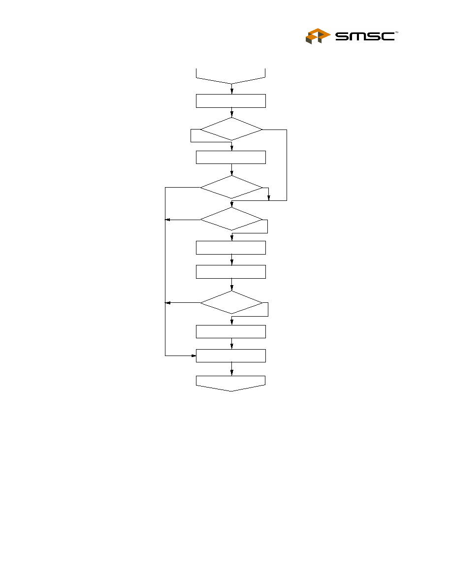
Non-PCI Single-Chip Full Duplex Ethernet Controller with Magic Packet
SMSC DS ≠ LAN91C965v&3v
Page 71
Rev. 09/10/2004
DATASHEET
RX INTR
Write Ad. Ptr. Reg. & Read
Word 0 from RAM
Destination
Multicast?
Read Words 2, 3, 4 from RAM
for Address Filtering
Address Filtering
Pass?
Status Word
OK?
Do Receive Lookahead
Get Copy Specs from Upper
Layer
Okay to
Copy?
Copy Data Per Upper Layer
Specs
Issue "Remove and Release"
Command
Return to ISR
Yes
No
Yes
No
No
Yes
No
Yes
Figure 8.2 - RX INTR

Non-PCI Single-Chip Full Duplex Ethernet Controller with Magic Packet
Rev. 09/10/2004
Page 72
SMSC LAN91C965v&3v
DATASHEET
TX Interrupt With AUTO_RELEASE = FALSE
1. Save the Packet Number Register
Saved_PNR = Read Byte (Bank 2, Offset 2)
2. Read the EPH Status Register
Temp = Read (Bank 0, Offset 2)
3. Acknowledge TX Interrupt
Write Byte (0x02, (Bank 2, Offset C));
4. Check for Status of Transmission
If ( Temp AND 0x0001)
{
//If Successful Transmission
Step 4.1.1: Issue MMU Release (Release Specific Packet)
Write (0x00A0, (Bank2, Offset 0));
Step 4.1.2: Return from the routine
}
else
{
//Transmission has FAILED
// Now we can either release or re-enqueue the packet
Step 4.2.1: Get the packet to release/re-enqueue, stored in FIFO
Temp = Read (Bank 2, Offset 4)
Temp = Temp & 0x003F
Step 4.2.2: Write to the PNR
Write (Temp, (Bank2, Offset 2))
Step
4.2.3
// Option 1: Release the packet
Write (0x00A0, (Bank2, Offset 0));
//Option 2: Re-Enqueue the packet
Write (0x00C0, (Bank2, Offset 0));
Step 4.2.4: Re-Enable Transmission
Temp = Read(Bank0, Offset 0);
Temp
=
Temp2
OR 0x0001
Write (Temp2, (Bank 0, Offset 0));
Step 4.2.5: Return from the routine
}
5. Restore the Packet Number Register
Write Byte (Saved_PNR, (Bank 2, Offset 2))
Figure 8.3 -TX INTR
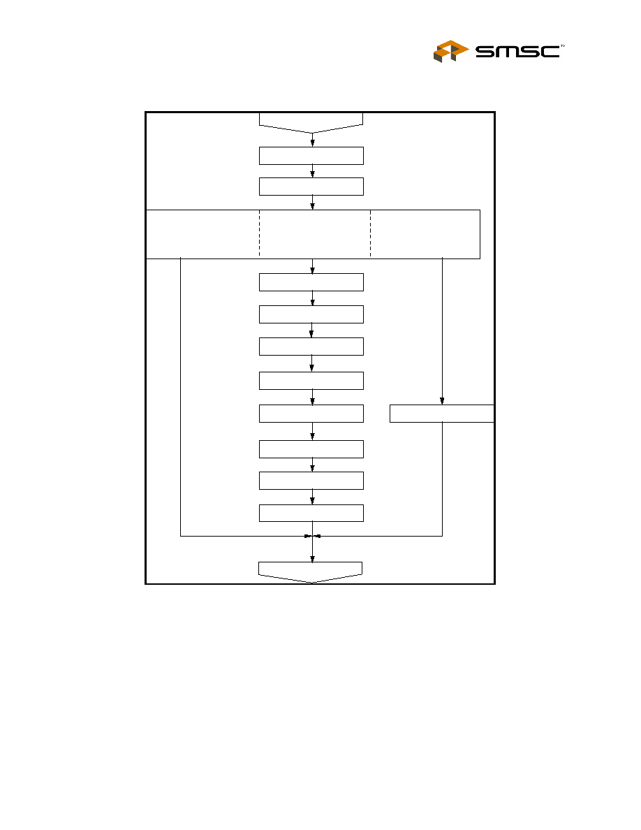
Non-PCI Single-Chip Full Duplex Ethernet Controller with Magic Packet
SMSC DS ≠ LAN91C965v&3v
Page 73
Rev. 09/10/2004
DATASHEET
Figure 8.4 -TXEMPTY INTR
(Assumes Auto Release Option Selected)
TXEMPTY INTR
Write Acknowledge Reg. with
TXEMPTY Bit Set
Read TXEMPTY & TX INTR
Acknowledge TXINTR
Re-Enable TXENA
Return to ISR
Issue "Release" Command
Restore Packet Number
TXEMPTY = 0
&
TXINT = 0
(Waiting for Completion)
TXEMPTY = X
&
TXINT = 1
(Transmission Failed)
TXEMPTY = 1
&
TXINT = 0
(Everything went through
successfully)
Read Pkt. # Register & Save
Write Address Pointer
Register
Read Status Word from RAM
Update Statistics
Update Variables
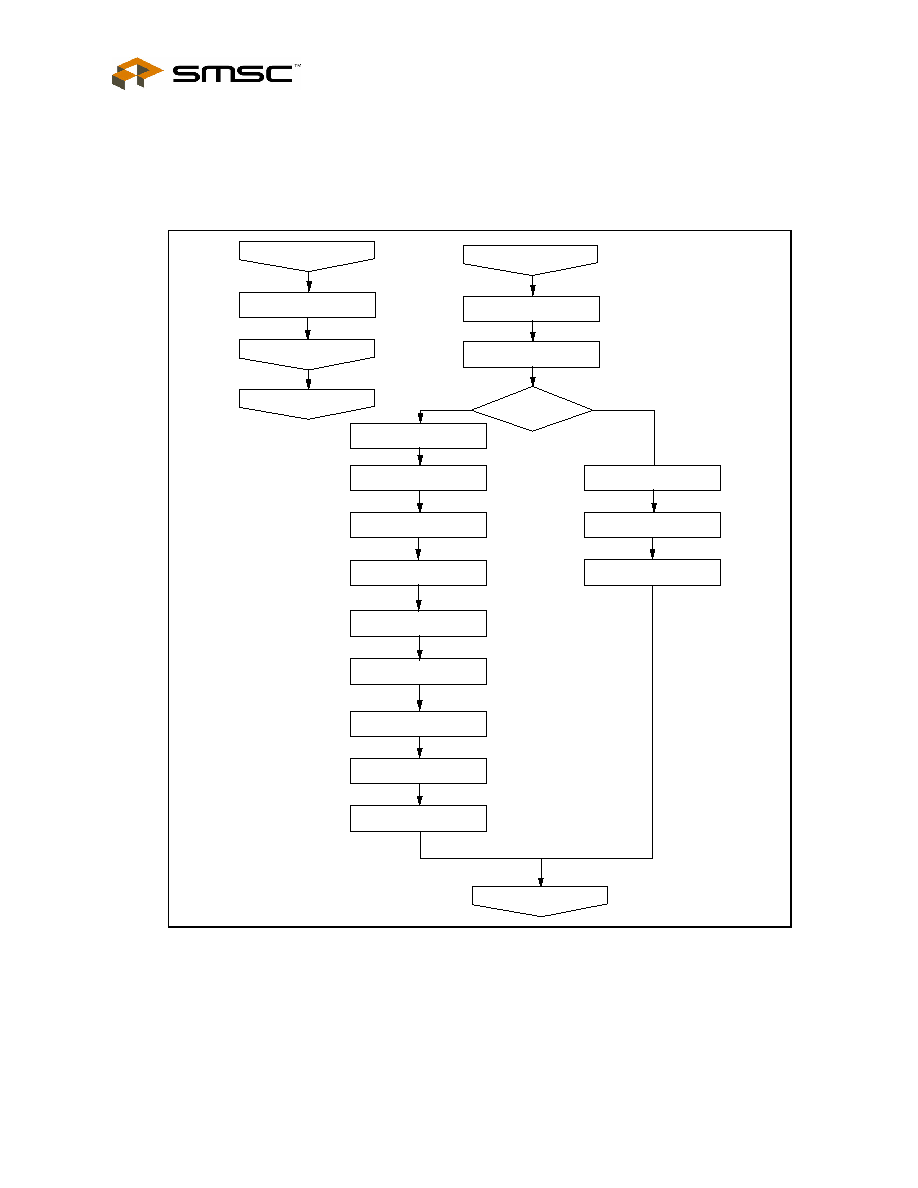
Non-PCI Single-Chip Full Duplex Ethernet Controller with Magic Packet
Rev. 09/10/2004
Page 74
SMSC LAN91C965v&3v
DATASHEET
Figure 8.5 ≠ Driver Send and Allocate Routines
ALLOCATE
Issue "Allocate Memory"
Command to MMU
Read Interrupt Status Register
Enqueue Packet
Set "Ready for Packet" Flag
Return
Copy Remaining TX Data
Packet into RAM
Return Buffers to Upper Layer
Write Allocated Packet into
Packet # Register
Write Address Pointer
Register
Copy Part of TX Data Packet
into RAM
Write Source Address into
Proper Location
Store Data Buffer Pointer
Clear "Ready for Packet" Flag
Enable Allocation Interrupt
Allocation
Passed?
Yes
No
DRIVER SEND
Choose Bank Select
Register 2
Call ALLOCATE
Exit Driver Send
Read Allocation Result
Register

Non-PCI Single-Chip Full Duplex Ethernet Controller with Magic Packet
SMSC DS ≠ LAN91C965v&3v
Page 75
Rev. 09/10/2004
DATASHEET
MEMORY PARTITIONING
Unlike other controllers, the LAN91C96 does not require a fixed memory partitioning between transmit and
receive resources. The MMU allocates and de-allocates memory upon different events. An additional
mechanism allows the CPU to prevent the receive process from starving the transmit memory allocation.
Memory is always requested by the side that needs to write into it, that is: The CPU for transmit or the
CSMA/CD for receive. The CPU can control the number of bytes it requests for transmit but it cannot
determine the number of bytes the receive process is going to demand. Furthermore, the receive process
requests will be dependent on network traffic, in particular on the arrival of broadcast and multicast
packets that might not be for the node, and that are not subject to upper layer software flow control.
In order to prevent unwanted traffic from using too much memory, the CPU can program a "memory
reserved for transmit" parameter. If the free memory falls below the "memory reserved for transmit" value,
MMU requests from the CSMA/CD block will fail and the packets will overrun and be ignored. Whenever
enough memory is released, packets can be received again. If the reserved value is too large, the node
might lose data which is an abnormal condition. If the value is kept at zero, memory allocation is handled
on first-come first-served basis for the entire memory capacity.
Note that with the memory management built into the LAN91C96, the CPU can dynamically program this
parameter. For instance, when the driver does not need to enqueue transmissions, it can allow more
memory to be allocated for receive (by reducing the value of the reserved memory). Whenever the driver
needs to burst transmissions it can reduce the receive memory allocation. The driver program the
parameter as a function of the following variables:
1. Free memory (read only register)
2. Memory size (read only register)
The reserved memory value can be changed on the fly. If the MEMORY RESERVED FOR TX value is
increased above the FREE MEMORY, receive packets in progress are still received, but no new packets
are accepted until the FREE MEMORY increases above the MEMORY RESERVED value.
INTERRUPT GENERATION
The interrupt strategy for the transmit and receive processes is such that it does not represent the
bottleneck in the transmit and receive queue management between the software driver and the controller.
For that purpose there is no register reading necessary before the next element in the queue (namely
transmit or receive packet) can be handled by the controller. The transmit and receive results are placed
in memory.
The receive interrupt will be generated when the receive queue (FIFO of packets) is not empty and receive
interrupts are enabled. This allows the interrupt service routine to process many receive packets without
exiting, or one at a time if the ISR just returns after processing and removing one.
There are two types of transmit interrupt strategies:
1. One interrupt per packet.
2. One interrupt per sequence of packets.
The strategy is determined by how the transmit interrupt bits and the AUTO RELEASE bit are used.
TX INT bit - Set whenever the TX completion FIFO is not empty.
TX EMPTY INT bit - Set whenever the TX FIFO is empty.
AUTO RELEASE - When set, successful transmit packets are not written into completion FIFO, and their
memory is released automatically.

Non-PCI Single-Chip Full Duplex Ethernet Controller with Magic Packet
Rev. 09/10/2004
Page 76
SMSC LAN91C965v&3v
DATASHEET
1. One interrupt per packet: enable TX INT, set AUTO RELEASE=0. The software driver can find the
completion result in memory and process the interrupt one packet at a time. Depending on the
completion code the driver will take different actions. Note that the transmit process is working in
parallel and other transmissions might be taking place. The LAN91C96 is virtually queuing the packet
numbers and their status words.
In this case, the transmit interrupt service routine can find the next packet number to be serviced by
reading the TX FIFO PACKET NUMBER at the FIFO PORTS register. This eliminates the need for
the driver to keep a list of packet numbers being transmitted. The numbers are queued by the
LAN91C96 and provided back to the CPU as their transmission completes.
2. One interrupt per sequence of packets: Enable TX EMPTY INT and TX INT, set AUTO RELEASE=1.
TX EMPTY INT is generated only after transmitting the last packet in the FIFO. TX INT will be set on
a fatal transmit error allowing the CPU to know that the transmit process has stopped and therefore
the FIFO will not be emptied.
This mode has the advantage of a smaller CPU overhead, and faster memory de-allocation. Note that
when AUTO RELEASE=1 the CPU is not provided with the packet numbers that completed
successfully.
Note:
The pointer register is shared by any process accessing the LAN91C96 memory. In order to allow
processes to be interruptible, the interrupting process is responsible for reading the pointer value before
modifying it, saving it, and restoring it before returning from the interrupt.
Typically there would be three processes using the pointer:
1) Transmit loading (sometimes interrupt driven)
2) Receive unloading (interrupt driven)
3) Transmit Status reading (interrupt driven).
1) and 3) also share the usage of the Packet Number Register. Therefore saving and restoring the PNR is
also required from interrupt service routines.
POWER DOWN
The LAN91C96 can enter power down mode by means of the PWRDWN pin (pin 68) or the PWRDN bit
(Control Register, bit 13). When in power down mode, the LAN91C96 will:
Stop the crystal oscillator
Tristate: Data Bus
-
Interrupts(only by PWRDN bit)
- nIOCS16
-
10BASE-T and AUI outputs
-
Turn off analog bias currents
Drive the EEPROM and ROM outputs inactive
Preserve contents of registers and memory
The PWRDWN pin is internally gated with the RESET (RESET pin before de-glitching) and with the
SRESET bit (COR bit 7). This gating function internally negates power down whenever RESET is high or
SRESET is high to allow the oscillator to run during RESET. Except for this gating function, all other uses
of the RESET pin use a de-glitched version of the signal as defined in the pin description section.

Non-PCI Single-Chip Full Duplex Ethernet Controller with Magic Packet
SMSC DS ≠ LAN91C965v&3v
Page 77
Rev. 09/10/2004
DATASHEET
NXENDEC PIN
PWRDN PIN
PWRDN BIT
0
1
1
X
X
0
1
X
0
0
0
1
Normal external ENDEC operation
Normal internal ENDEC operation
Powerdown - Normal mode restored by
PWRDWN pin going low
Powerdown - Bit is cleared by a write
access to any LAN91C96 register or by
hardware reset
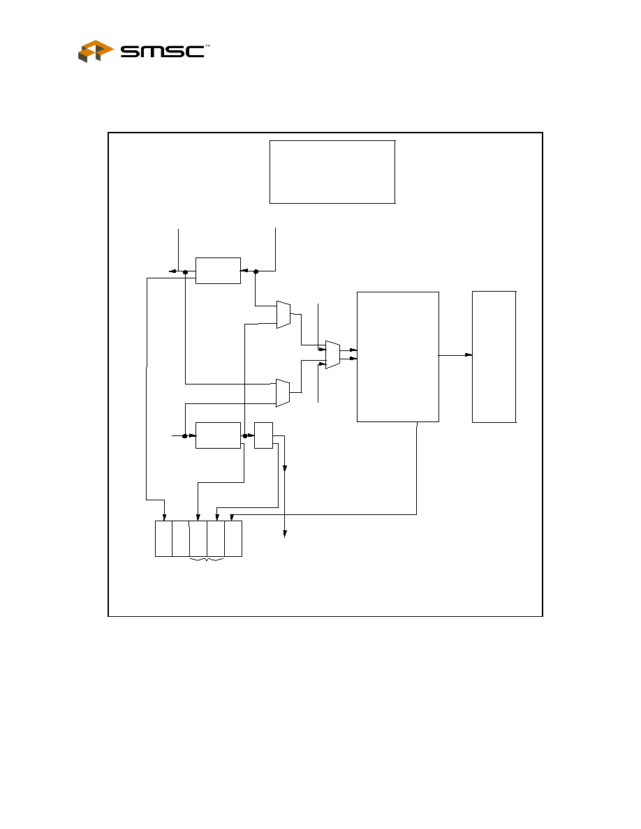
Non-PCI Single-Chip Full Duplex Ethernet Controller with Magic Packet
Rev. 09/10/2004
Page 78
SMSC LAN91C965v&3v
DATASHEET
Figure 8.6 ≠ Interrupt Generation for Transmit; Receive, MMU
T
X
F
I
F
O
T
X
CO
M
P
L
E
T
I
O
N
F
I
F
O
RX
F
I
F
O
C
S
M
A
/
C
D
L
O
G
I
C
A
L
A
D
D
RE
S
S
P
A
C
K
E
T
#
M
M
U
P
H
Y
S
I
CA
L
A
D
DR
E
S
S
R
A
M
CP
U A
DDRE
S
S
CS
M
A
A
D
DRE
S
S
RX P
A
CKE
T
NUMB
E
R
R
X
FI
FO
P
A
CK
E
T
NUM
B
E
R
P
A
CK
E
T
NUM
B
E
R
RE
G
I
S
T
ER
PA
C
K
#
O
U
T
M.
S.
BI
T
O
N
L
Y
'E
M
P
T
Y
'
'
N
O
T
EM
PT
Y
'
TX
D
O
N
E
P
A
CK
ET
NUM
B
E
R
'
N
O
T
E
M
PT
Y'
IN
TE
R
R
U
P
T
S
T
A
T
US
RE
G
I
S
T
E
R
RC
V
IN
T
T
X
EMPT
Y
IN
T
TX
IN
T
A
LLO
C
IN
T
TW
O
OPT
I
O
N
S

Non-PCI Single-Chip Full Duplex Ethernet Controller with Magic Packet
SMSC DS ≠ LAN91C965v&3v
Page 79
Rev. 09/10/2004
DATASHEET
Chapter 9 Functional Description of the Blocks
9.1 Memory
Management
Unit
The MMU interfaces the on-chip RAM on one side and the arbiter on the other for address and data flow
purposes. For allocation and de-allocation, it interfaces the arbiter only.
The MMU deals with a single ported memory and is not aware of the fact that there are two entities
requesting allocation and actually accessing memory. The mapping function done by the MMU is only a
function of the packet number accessed and of the offset within that packet being accessed. It is not a
function of who is requesting the access or the direction of the access.
To accomplish that, memory accesses as well as MMU allocation and de-allocation requests are arbitrated
by the arbiter block before reaching the MMU.
Memory allocation could take some time, but the ALLOC INT bit in Interrupt Status Register is negated
immediately upon allocation request, allowing the system to poll that register at any time. Memory de-
allocation command completion indication is provided via the BUSY bit, readable through the MMU
command register.
The mapping and queuing functions of the MMU rely on the uniqueness of the packet number assigned to
the requester. For that purpose the packet number assignment is centralized at the MMU, and a number
will not be reused until the memory associated with it is released. It is clear that a packet number should
not be released while the number is in the TX or RX packet queue.
The TX and RCV FIFOs are deep enough to handle the total number of packets the MMU can allocate,
therefore there is no need for the programmer or the hardware to check FIFO full conditions.
9.2 Arbiter
The function of the arbiter is to sequence packet RAM accesses as well as MMU requests in such a way
that the on-chip single ported RAM and a single MMU can be shared by two parties. One party is the host
CPU and the other party is the CSMA/CD block.
The arbiter is address transparent, namely, any address can be accessed at any time. In order to exploit
the sequential nature of the access, and minimize the access time on the system side, the CPU cycle is
buffered by the Data Register rather than go directly to and from memory. Whenever a write cycle is
performed, the data is written into the Data Register and will be written into memory as a result of that
operation, allowing the CPU cycle to complete before the arbitration and memory cycle are complete.
Whenever a read cycle is performed, the data is provided immediately from the Data Register, without
having to arbitrate and complete a memory cycle. The present cycle results in an arbitration request for
the next data location. Loading the pointer causes a similar pre-fetch request.
This type of read-ahead and write-behind arbitration allows the controller to have a very fast access time,
and would work without wait states for as long as the cycle time specification is satisfied. The values are
40 ns access time, and 185ns cycle time.
By the same token, CSMA/CD cycles might be postponed. The worst case CSMA/CD latency for arbiter
service is one memory cycle. The arbiter uses the pointer register as the CPU provided address, and the
internal DMA address from the CSMA/CD side as the addresses to be provided to the MMU.

Non-PCI Single-Chip Full Duplex Ethernet Controller with Magic Packet
Rev. 09/10/2004
Page 80
SMSC LAN91C965v&3v
DATASHEET
The data path routed by the arbiter goes between memory (the data path does not go through the MMU)
on one side and either the CPU side bus or the data path of the CSMA/CD core.
The data path between memory and the Data Register is in fact buffered by a small FIFO in each direction.
The FIFOs beneath the Data Register can be read and written as bytes or words, in any sequential
combination. The presence of these FIFOs makes sure that word transfers are possible on the system bus
even if the address loaded into the pointer is odd.
9.3 Bus
Interface
The bus interface handles the data, address and control interfaces and is compliant with the LOCAL BUS,
PCMCIA, and 68000-interface specifications and allows 8 or 16 bit adapters to be designed with the
LAN91C96 with no glue to interface the LOCAL BUS or PCMCIA bus.
The functions in this block include address decoding for I/O and ROM memory (including address
relocation support) for LOCAL BUS, data path routing, sequential memory address support, optional wait
state generation, boot ROM support, EEPROM setup function, bus transceiver control, and interrupt
generation / selection.
For LOCAL BUS, I/O address decoding is done by comparing A15-A4 to the I/O BASE address
determined in part by the upper byte of the BASE ADDRESS REGISTER, and also requiring that AEN be
low. If the above address comparison is satisfied and the LAN91C96 is in 16 bit mode, nIOCS16 will be
asserted (low).
A valid comparison does not yet indicate a valid I/O cycle is in progress, as the addresses could be used
for a memory cycle, or could even glitch through a valid value. For LOCAL BUS and PCMCIA, only
when nIORD or nIOWR are activated the I/O cycle begins.
In PCMCIA mode, A4-A15 are ignored for I/O decodes, which rely on the PCMCIA host, decoding for the
slot. Input A10 for LOCAL BUS is used as an output (nFWE) for PCMCIA to enable Flash Memory Write
for programming the attribute memory. It is valid only when nWE is "0" and COR2 is "1". nA11/nFCS is
used to select the Flash Memory Chip.
The LAN91C96 provides a glueless interface to a stripped down version of the Motorola 68000 processor.
This interface is limited to 16 bits only. None of the size or function pins are supported. The LAN91C96
functions as a slave and requires some of its pins pulled high or low for the interface to function.
The SMC91C96 enters the 68000 interface mode when nIORD and nIOWR are asserted simultaneously.
Once the two are asserted together, the only way to return to the LOCAL BUS interface is by hard
resetting the chip. Notice that the chip is required to power up in LOCAL BUS mode to use the 68000
interface.
For the first chip access, the first transfer (to the 91C96) must be a write as the controller uses this write to
confirm the 68000 mode. The LAN91C96 responds to addresses per the base address register contents
(as in the LOCAL BUS mode).
9.4
Wait State Policy
The LAN91C96 can work on most system buses without having to add wait states. The two parameters
that determine the memory access profile are the read access time and the cycle time into the Data
Register.
The read access time is 40ns and the cycle time is 185ns. If any one of them does not satisfy the
application requirements, wait states should be added.

Non-PCI Single-Chip Full Duplex Ethernet Controller with Magic Packet
SMSC DS ≠ LAN91C965v&3v
Page 81
Rev. 09/10/2004
DATASHEET
If the access time is the problem, IOCHRDY should be negated for all accesses to the LAN91C96. This
can be achieved by programming the NO WAIT ST bit in the configuration register to "0". The LAN91C96
will negate IOCHRDY for 100ns to 150ns on every access to any register.
If the cycle time is the problem, programming NO WAIT ST as described before will solve it but at the
expense of slowing down all accesses. The alternative is to let the LAN91C96 negate IOCHRDY only
when the Data Register FIFOs require so. Namely, if NO WAIT ST is set, IOCHRDY will only be negated if
a Data Register read cycle starts and there is less than a full word in the read FIFO, or if a write cycle
starts and there is more than two bytes in the write FIFO.
The cycle time is defined as the time between leading edges of read from the Data Register, or
equivalently between trailing edges of write to the Data Register. For example, in an LOCAL BUS system
the cycle time of a 16 bit transfer will be at least 2 clocks for the I/O access to the LAN91C96 (+ one clock
for the memory cycle) for a total of 3 clocks. In absolute time it means 375ns for an 8MHz bus, and 240ns
for a 12.5 MHz bus.
The cycle time will not increase when configured for full duplex mode, because the CSMA/CD memory
arbitration requests are sequenced by the DMA logic and never overlap.
9.5 Arbitration
Considerations
The arbiter exploits the sequential nature of the CPU accesses to provide a very fast access time. Memory
bandwidth considerations will have an effect on the CPU cycle time but no effect on access time.
For normal 8MHz, 10MHz, and 12.5MHz LOCAL BUS, as well as EISA normal cycles, the LAN91C96 can
be accessed without negating ready.
When write operations occur, the data is written into a FIFO. The CPU cycle can complete immediately,
and the buffered data will be written into memory later. The memory arbitration request is generated as a
function of that FIFO being not empty. The nature of the cycle requested (byte/word) is determined by the
LSB of the pointer and the number of bytes in the FIFO.
When read operations occur, words are pre-fetched upon pointer loading in order to have at least a word
ready in the FIFO to be read. New pre-fetch cycles are requested as a function of the number of bytes in
the FIFO.
For example, if an odd pointer value is loaded, first a byte is pre-fetched into the FIFO, and immediately a
full word is pre-fetched completing three bytes into the FIFO. If the CPU reads a word, one byte will be left
again a new word is pre-fetched.
In the case of write, if an odd pointer value is loaded, and a full word is written, the FIFO holds two bytes,
the first of which is immediately written into an odd memory location. If by that time another byte or word
was written, there will be two or three bytes in the FIFO and a full word can be written into the now even
memory address.
When a CSMA/CD cycle begins, the arbiter will route the CSMA/CD DMA addresses to the MMU as well
as the packet number associated with the operation in progress. In full-duplex mode, receive and transmit
requests are alternated in such a way that the CPU arbitration cycle time is not affected.
9.6 DMA
Block
The DMA block resides between the CSMA/CD block and the arbiter. It can interface both the data path
and the control path of the CSMA/CD block for different operations.
Its functions include the following:

Non-PCI Single-Chip Full Duplex Ethernet Controller with Magic Packet
Rev. 09/10/2004
Page 82
SMSC LAN91C965v&3v
DATASHEET
Start transmission process into the CSMA/CD block.
Generate CSMA/CD side addresses for accessing memory during transmit and receive operations.
Generate MMU memory requests and verify success.
Compute byte count and write it in first locations of receive packet.
Write transmit status word in first locations of transmit packet.
Determine if enough memory is available for reception.
De-allocate transmit memory after suitable completion.
De-allocate receive memory upon error conditions.
Initiate retransmissions upon collisions (if less than 16 retries).
Terminate reception and release memory if packet is too long.
The specific nature of each operation and its trigger event are:
1. TX operations will begin if TXENA is set and TX FIFO is not empty. The DMA logic does not need to
use the TX PACKET NUMBER, it goes directly from the FIFO to the MMU. However the DMA logic
controls the removal of the PACKET NUMBER from the FIFO.
2. Generation of CSMA/CD side addresses into memory: Independent 11-bit counters are kept for
transmit and receive in order to allow full-duplex operation.
3. MMU requests for allocation are generated by the DMA logic upon reception. The initial allocation
request is issued when the CSMA block indicates an active reception. If allocation succeeds, the DMA
block stores the packet number assigned to it, and generates write arbitration requests for as long as
the CSMA/CD FIFO is not empty. In parallel the CSMA/CD completes the address filtering and
notifies the DMA of an address match. If there is no address match, the DMA logic will release the
allocated memory and stop reception.
4. When the CSMA/CD block notifies the DMA logic that a receive packet was completed, if the CRC is
OK, the DMA will either write the previously stored packet number into the RX PACKET NUMBER
FIFO (to be processed by the CPU), or if the CRC is bad the DMA will just issue a release command
to the MMU (and the CPU will never see that packet).
Packets with bad CRC can be received if the RCV_BAD bit in the configuration register is set.
5. If AUTO_RELEASE is set, a release is issued by the DMA block to the MMU after a successful
transmission (TX_SUCC set), and the TX completion FIFO is clocked together with the TX FIFO
preventing the packet number from moving into the TX completion FIFO.
6. Based on the RX counter value, if a receive packet exceeds 1532 bytes, reception is stopped by the
DMA and the RX ABORT bit in the Receive Control Register is set. The memory allocated to the
packet is automatically released.
7. If an allocation fails, the CSMA/CD block will activate RX_OVRN INT upon detecting a FIFO full
condition. RXEN will stay active to allow reception of subsequent packets if memory becomes
available. The CSMA/CD block will flush the FIFO upon the new frame arrival.
9.7
Packet Number FIFOS
The transmit packet FIFO stores the packet numbers awaiting transmission, in the order they were
enqueued. The FIFO is advanced (written) when the CPU issues the "enqueue packet number
command", the packet number to be written is provided by the CPU via the Packet Number Register. The
number was previously obtained by requesting memory allocation from the MMU. The FIFO is read by the
DMA block when the CSMA/CD block is ready to proceed on to the next transmission. By reading the TX
EMPTY INT bit the CPU can determine if this FIFO is empty.
The transmit completion FIFO stores the packet numbers that were already transmitted but not yet
acknowledged by the CPU. The CPU can read the next packet number in this FIFO from the FIFO Ports
Register. The CPU can remove a packet number from this FIFO by issuing a TX INT acknowledge. The
CPU can determine if this FIFO is empty by reading the TX INT bit or the FIFO Ports Register.

Non-PCI Single-Chip Full Duplex Ethernet Controller with Magic Packet
SMSC DS ≠ LAN91C965v&3v
Page 83
Rev. 09/10/2004
DATASHEET
The receive packet FIFO stores the packet numbers already received into memory, in the order they were
received. The FIFO is advanced (written) by the DMA block upon reception of a complete valid packet into
memory. The number is determined the moment the DMA block first requests memory from the MMU for
that packet. The first receive packet number in the FIFO can be read via the FIFO Ports Register, and the
data associated with it can be accessed through the receive area. The packet number can be removed
from the FIFO with or without an automatic release of its associated memory.
The FIFO is read out upon CPU command (remove packet from top of RX FIFO, or remove and release
command) after processing the receive packet in the receive area.
The width of each FIFO is 5 bits per packet number. The depth of each FIFO equals the number of
packets the LAN91C96 can handle (18).
The guideline is software transparency; the software driver should not be aware of different devices or
FIFO depths. If the MMU memory allocation succeeded, there will be room in the transmit FIFO for
enqueuing the packet. Conversely if there is free memory for receive, there should be room in the receive
FIFO for storing the packet number.
Note that the CPU can enqueue a transmit command with a packet number that does not follow the
sequence in which the MMU assigned packet numbers. For example, when a transmission failed and it is
retried in software, or when a receive packet is modified and sent back to the network.
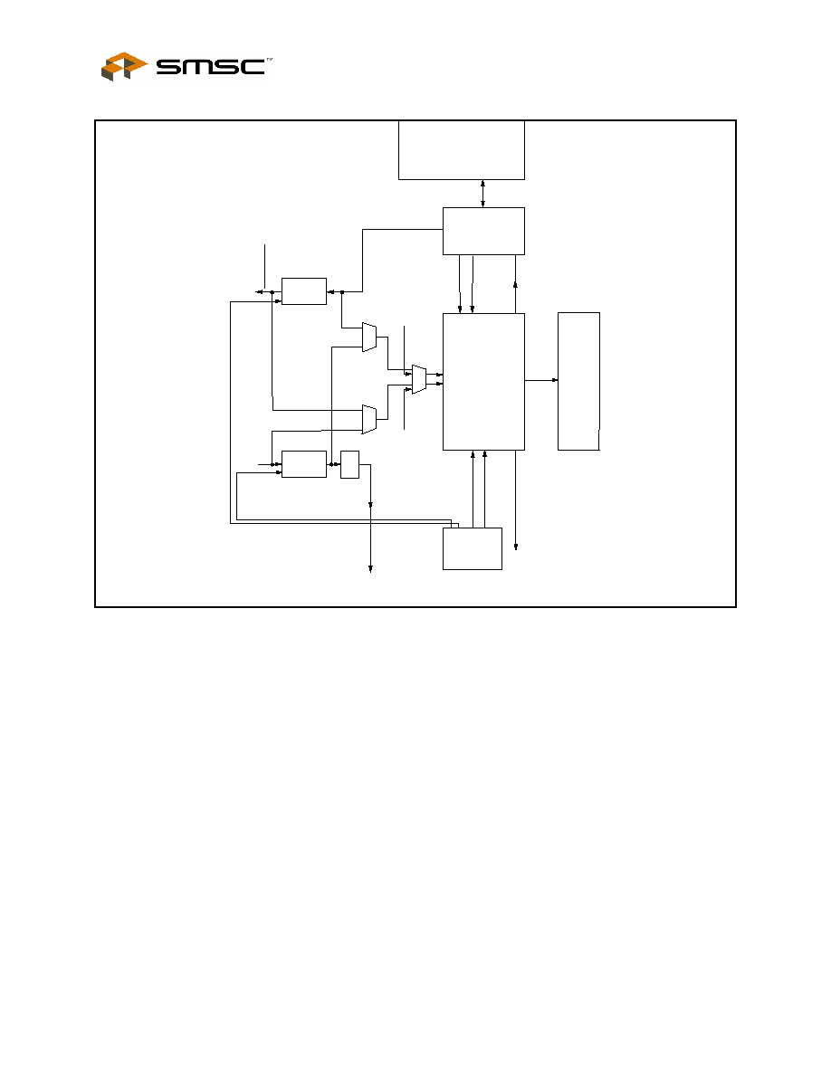
Non-PCI Single-Chip Full Duplex Ethernet Controller with Magic Packet
Rev. 09/10/2004
Page 84
SMSC LAN91C965v&3v
DATASHEET
T
X
F
I
F
O
C
O
M
P
L
E
T
I
O
N
F
I
F
O
R
X
F
I
F
O
C
S
M
A
/
C
D
L
O
G
I
C
A
L
A
D
D
R
E
S
S
P
A
C
K
E
T
#
M
M
U
P
H
Y
S
I
C
A
L
A
D
D
R
E
S
S
R
A
M
CP
U A
DDRE
S
S
CS
M
A
ADDRE
S
S
R
X
P
A
CKET
NUMB
E
R
RX
F
I
F
O
PA
C
K
E
T
N
U
M
B
E
R
P
A
CKE
T
NUMB
E
R
R
E
G
I
STER
PA
C
K
#
O
U
T
TX D
O
N
E
P
A
C
KET
N
U
M
BER
AL
LO
C
A
TI
O
N
RES
U
L
T
R
E
G
I
STE
R
AL
LO
C
A
TE
R
E
L
EAS
E
PA
C
K
#
O
U
T
DM
A
RD
WR
TX
D
E
CODE
R
MM
U
COMMA
ND
R
E
G
I
STER
ALL
O
C
A
TE
R
E
L
EASE
IN
T
FIGURE 9.1 - MMU PACKET NUMBER FLOW AND RELEVANT REGISTERS
9.8 CSMA
Block
The CSMA/CD block is first interfaced via its control registers in order to define its operational
configuration. From then on, the DMA interface between the CSMA/CD block and memory is used to
transfer data to and from its data path interface.
For transmit, the CSMA/CD block will be asked to transmit frames as soon as they are ready in memory. It
will continue transmissions until any of the following transmit error occurs:
1. Collisions on same frame
2. Late
collision
3. Lost Carrier sense and MON_CSN set
4. Transmit
Underrun
5. SQET error and STP_SQET set

Non-PCI Single-Chip Full Duplex Ethernet Controller with Magic Packet
SMSC DS ≠ LAN91C965v&3v
Page 85
Rev. 09/10/2004
DATASHEET
In that case TXENA will be cleared and the CPU should restart the transmission by setting it again. If a
transmission is successful, TXENA stays set and the CSMA/CD is provided by the DMA block with the
next packet to be transmitted.
For receive, the CPU sets RXEN as a way of starting the CSMA/CD block receive process. The CSMA/CD
block will send data after address filtering through the data path to the DMA block. Data is transferred into
memory as it is received, and the final check on data acceptance is the CRC checking done by the
CSMA/CD block. In any case, the DMA takes care of requesting/releasing memory for receive packets, as
well as generating the byte count.
The receive status word is provided by the CSMA/CD block and written in the first location of the receive
structure by the DMA block. If configured for storing CRC in memory, the CSMA/CD unit will transfer the
CRC bytes through the DMA interface, and then will be treated like regular data bytes.
Note that the receive status word of any packet is available only through memory and is not readable
through any other register. In order to let the CPU know about receive overruns, the RX_OVRN INT is set
and latched in the Interrupt Status Register, which is readable by the CPU at any time.
The address filtering is done inside the CSMA/CD block. A packet will be received if the destination
address is broadcast, or if it is addressed to the individual address of the LAN91C96, or if it is a multicast
address and ALMUL bit is set, or if it is a multicast address matching one of the multicast table entries. If
the PRMS bit is set, all packets are received. The CSMA/CD block is a full duplex machine, and when
working in full duplex mode, the CSMA/CD block will be simultaneously using its data path transmit and
receive interfaces.
Statistical counters are kept by the CSMA/CD block, and are readable through the appropriate register.
The counters are four bits each, and can generate an interrupt when reaching their maximum values.
Software can use that interrupt to update statistics in memory, or it can keep the counter interrupt disabled,
while relying on the transmit interrupt routine reading the counters. Given that the counters can increment
only once per transmit, this technique is a good complement for the single interrupt per sequence strategy.
The interface between the CSMA/CD block and memory is word oriented. Two bi-directional FIFOs make
the data path interface.
Whenever a normal collision occurs (less than 16 retries), the CSMA/CD will trigger the backoff logic and
will indicate the DMA logic of the collision. The DMA is responsible for restarting the data transfer into the
CSMA/CD block regardless of whether the collision happened on the preamble or not.
Only when 16 retries are reached, the CSMA/CD block will clear the TXENA bit, and CPU intervention is
required. The DMA will not automatically restart data transfer in this case, nor will it transmit the next
enqueued packet until TXENA is set by the CPU. The DMA will move the packet number in question from
the TX FIFO into the TX completion FIFO.
9.9 Network
Interface
The LAN91C96 includes both an AUI interface for thick and thin coax applications and a 10BASE-T
interface for twisted pair applications. Functions common to both are:
1. Manchester encoder/decoder to convert NRZ data to Manchester encoded data and back.
2. A 32ms jabber timer to prevent inadvertently long transmissions. When 'jabbing' occurs, the
transmitter is disabled, automatic loopback is disabled (in 10BASE-T mode), and a collision indication
is given to the controller. The interface 'unjabs' when the transmitter has been idle for a minimum of
256 ms.
3. A phase-lock loop to recover data and clock from the Manchester data stream with up to plus or minus
18ns of jitter.
4. Diagnostic loopback capability.

Non-PCI Single-Chip Full Duplex Ethernet Controller with Magic Packet
Rev. 09/10/2004
Page 86
SMSC LAN91C965v&3v
DATASHEET
5. LED drivers for collision, transmission, reception, and jabber.
9.10 10Base-T
The 10BASE-T interface conforms to the twisted pair MAU addendum to the 802.3 specification. On the
transmission side, it converts the NRZ data from the controller to Manchester data and provides the
appropriate signal level for driving the media. Signal are predistorted before transmission to minimize ISI.
The collision detection circuitry monitors the simultaneous occurrence of received signals and transmitted
data on the media. During transmission, data is automatically looped back to the receiver except during
collision periods, in which case the input to the receiver is network data. During collisions, should the
receive input go idle prior to the transmitter going idle, input to the receiver switches back to the transmitter
within nine bit times. Following transmission, the transmitter performs a SQE test. This test exercises the
collision detection circuitry within the 10BASE-T interface.
The receiver monitors the media at all times. It recovers the clock and data and passes it along to the
controller. In the absence of any receive activity, the transmitter is looped back to the receiver. In addition,
the receiver performs automatic polarity correction. The 10BASE-T interface performs link integrity tests
per section 14.2.1.7 of 802.3, using the following values:
1. Link_loss_timer: 64 ms
2. Link_test_min_timer: 4 ms
3. Link_count:
2
4. Link_test_max_timer: 64 ms
The state of the link is reflected in the EPHSR.
9.11 AUI
The LAN91C96 also provides a standard six wire AUI interface to a coax transceiver.
9.12 Physical
Interface
The internal physical interface (PHY) consists of an encoder/decoder (ENDEC) and an internal 10BASE-T
transceiver. The ENDEC also provides a standard 6-pin AUI interface to an external coax transceiver for
10BASE-2 and 10BASE-5 applications. The internal signals between MAC and the PHY can be routed to
pins by asserting the nXENDEC pin low. This feature allows the interface to an external ENDEC and
transceiver. The PHY functions can be divided into transmit and receive functions.
9.13 Transmit
Functions
9.13.1 Manchester Encoding
The PHY encodes the transmit data received from the MAC. The encoded data is directed internally to the
selected output driver for transmission over the twisted-pair network or the AUI cable. Data transmission
and encoding is initiated by the Transmit Enable input, TXE, going low.

Non-PCI Single-Chip Full Duplex Ethernet Controller with Magic Packet
SMSC DS ≠ LAN91C965v&3v
Page 87
Rev. 09/10/2004
DATASHEET
9.13.2 Transmit Drivers
The encoded transmit data passes through to the transmit driver pair, TPETXP(N), and its complement,
TPETXDP(N). Each output of the transmit driver pair has a source resistance of 10 ohms maximum and a
current rating of 25 mA maximum. The degree of predistortion is determined by the termination resistors;
the equivalent resistance should be 100 ohms.
9.13.3 Jabber Function
This integrated function prevents the DTE from locking into a continuous transmit state. In 10BASE-T
mode, if transmission continues beyond the specified time limit, the jabber function inhibits further
transmission and asserts the collision indicator nCOLL. The limits for jabber transmission are 20 to 15 ms
in 10BASE-T mode. In the AUI mode, the jabber function is performed by the external transceiver.
9.13.4 SQE Function
In the 10BASE-T mode, the PHY supports the signal quality error (SQE) function. At the end of a
transmission, the PHY asserts the nCOLL signal for 10+/-5 bit times beginning 0.6 to 1.6ms after the last
positive transition of a transmitted frame. In the AUI mode, the SQE function is performed by the external
transceiver.
9.14 Receive
Functions
9.14.1 Receive Drivers
Differential signals received off the twisted-pair network or AUI cable are directed to the internal clock
recovery circuit prior to being decoded for the MAC.
9.14.2 Manchester Decoder and Clock Recovery
The PHY performs timing recovery and Manchester decoding of incoming differential signals in 10BASE-T
or AUI modes, with its built-in phase-lock loop (PLL). The decoded (NRZ) data, RXD, and the recovered
clock, RXCLK, becomes available to the MAC, typically within 9 bit times (5 for AUI) after the assertion of
nCRS. The receive clock, RXCLK, is phase-locked to the transmit clock in the absence of a received
signal (idle).
9.14.3 Squelch Function
The integrated smart squelch circuit employs a combination of amplitude and timing measurements to
determine the validity of data received off the network. It prevents noise at the differential inputs from
falsely triggering the decoder in the absence of valid data or link test pulses. Signal levels below 300mV
(180mV for AUI) or pulse widths less than 15ns at the differential inputs are rejected. Signals above
585mV (300mV for AUI) and pulse widths greater than 30ns will be accepted. When using the extended
cable mode with 10BASE-T media which extends beyond the standard limit of 100 meters, the squelch
level can optionally be set to reject signals below 180mV and accept signals above 300mV. If the input
signal exceeds the squelch requirements, the carrier sense output, nCRS, is asserted.

Non-PCI Single-Chip Full Duplex Ethernet Controller with Magic Packet
Rev. 09/10/2004
Page 88
SMSC LAN91C965v&3v
DATASHEET
9.14.4 Reverse Polarity Function
In the 10BASE-T mode, the PHY monitors for receiver polarity reversal due to crossed wires and corrects
by reversing the signal internally.
9.14.5 Collision Detection Function
In the 10BASE-T mode, a collision state is indicated when there are simultaneous transmissions and
receptions on the twisted pair link. During a collision state, the nCOLL signal is asserted. If the received
data ends and the transmit control signal is still active, the transmit data is sent to the MAC within 9 bit
times. The nCOLL signal is de-asserted within 9 bit times after the collision terminates. In the AUI mode,
the external transceiver sends a 10MHz signal to the PHY upon detection of a collision.
9.14.6 Link Integrity
The PHY test for a faulty twisted-pair link. In the absence of transmit data, link test pulses are transmitted
every 16+/-8ms after the end of the last transmission or link pulse on the twisted pair medium. If neither
valid data nor link test pulses are received within 10 to 150ms, the link is declared bad and both data
transmission as well as the operational loopback function are disabled. The Link Integrity function can be
disabled for pre-10BASE-T twisted-pair networks.

Non-PCI Single-Chip Full Duplex Ethernet Controller with Magic Packet
SMSC DS ≠ LAN91C965v&3v
Page 89
Rev. 09/10/2004
DATASHEET
Chapter 10 Board Setup Information
REGISTER
EEPROM WORD
ADDRESS
Configuration Register
Base Register
IOS Value * 4
(IOS Value *4) + 1
The following parameters are obtained from the EEPROM as board setup information:
ETHERNET INDIVIDUAL ADDRESS
I/O BASE ADDRESS
ROM BASE ADDRESS
8/16 BIT ADAPTER
10BASE-T or AUI INTERFACE
INTERRUPT LINE SELECTION
All the above mentioned values are read from the EEPROM upon hardware reset. Except for the
INDIVIDUAL ADDRESS, the value of the IOS switches determines the offset within the EEPROM for these
parameters, in such a way that many identical boards can be plugged into the same system by just
changing the IOS jumpers.
In order to support a software utility based installation, even if the EEPROM was never programmed, the
EEPROM can be written using the LAN91C96. One of the IOS combination is associated with a fixed
default value for the key parameters (I/O BASE, ROM BASE, INTERRUPT) that can always be used
regardless of the EEPROM based value being programmed. This value will be used if all IOS pins are left
open or pulled high.
The EEPROM is arranged as a 64 x 16 array. The specific target device is the 9346 1024-bit Serial
EEPROM. All EEPROM accesses are done in words. All EEPROM addresses shown are specified as
word addresses.
INDIVIDUAL ADDRESS 20-22 hexIf IOS2-0 = 7, only the INDIVIDUAL ADDRESS is read from the
EEPROM. Currently assigned values are assumed for the other registers. These values are default if the
EEPROM read operation follows hardware reset.
The EEPROM SELECT bit is used to determine the type of EEPROM operation: a) normal or b) general
purpose register.
a) NORMAL EEPROM OPERATION - EEPROM SELECT bit = 0
On EEPROM read operations (after reset or after setting RELOAD high) the CONFIGURATION
REGISTER and BASE REGISTER are updated with the EEPROM values at locations defined by the
IOS2-0 pins. The INDIVIDUAL ADDRESS registers are updated with the values stored in the
INDIVIDUAL ADDRESS area of the EEPROM.
On EEPROM write operations (after setting the STORE bit) the values of the CONFIGURATION
REGISTER and BASE REGISTER are written in the EEPROM locations defined by the IOS2-0 pins.
The three least significant bits of the CONTROL REGISTER (EEPROM SELECT, RELOAD and
STORE) are used to control the EEPROM. Their values are not stored nor loaded from the EEPROM.
b) GENERAL PURPOSE REGISTER - EEPROM SELECT bit = 1
On EEPROM read operations (after setting RELOAD high) the EEPROM word address defined by the
POINTER REGISTER 6 least significant bits is read into the GENERAL PURPOSE REGISTER.

Non-PCI Single-Chip Full Duplex Ethernet Controller with Magic Packet
Rev. 09/10/2004
Page 90
SMSC LAN91C965v&3v
DATASHEET
On EEPROM write operations (after setting the STORE bit) the value of the GENERAL PURPOSE
REGISTER is written at the EEPROM word address defined by the POINTER REGISTER 6 least
significant bits.
RELOAD and STORE are set by the user to initiate read and write operations respectively. Polling the
value until read low is used to determine completion. When an EEPROM access is in progress the
STORE and RELOAD bits of CTR will read-back as both bits high. No other bits of the LAN91C96
can be read or written until the EEPROM operation completes and both bits are clear. This
mechanism is also valid for reset initiated reloads.
Note:
If no EEPROM is connected to the LAN91C96, the ENEEP pin should be grounded and no accesses to
the EEPROM will be attempted. Configuration, Base and Individual Addresses assume their default values
upon hardware reset and the CPU is responsible for programming them for their final value.
10.1 Diagnostic
LEDs
The following LED drive signals are available for diagnostic and installation aid purposes:
nTXLED - Activated by transmit activity.
nBSELED - Board select LED. Activated when the board space is accessed, namely on accesses to the
LAN91C96 register space or the ROM area decoded by the LAN91C96. The signal is stretched to 125
msec.
nRXLED - Activated by receive activity.
nLINKLED - Reflects the link integrity status.
10.2 Bus Clock Considerations
The arbiter exploits the sequential nature of the CPU accesses to provide a very fast access time.
Memory bandwidth considerations will have an effect on the CPU cycle time but no effect on access time.
For normal 8MHz, 10MHz, and 12.5MHz LOCAL BUS, as well as EISA normal cycles, the LAN91C96 can
be accessed without negating ready.
See Arbitration Considerations in Functional Description of the Blocks for more details.
10.3 68000 Bus Interface
The LAN91C96 enters the 68000 interface mode when nIORD and nIOWR are asserted simultaneously.
Once the two are asserted together, the only way to return to the LOCAL BUS interface is by hard
resetting the chip. Notice that the chip is required to power up in LOCAL BUS mode to use the 68000
interface.
For the first chip access, the first transfer (to the LAN91C96) must be a write. The LAN91C96 uses this
write to confirm the 68000 mode. An attempted read may return incorrect data. The LAN91C96 responds
to addresses per the base address register contents (as in LOCAL BUS mode). Notice that the worst case
access time for the first cycle is the same as that for LOCAL BUS or PCMCIA modes.
The following is the Motorola 68000 Processor and the LAN91C96 pin mapping:
DS, LDS, or UDS to nIORD/xDS
R/nW to nIOWR/R/nW
Non-PCI Single-Chip Full Duplex Ethernet Controller with Magic Packet
SMSC DS ≠ LAN91C965v&3v
Page 91
Rev. 09/10/2004
DATASHEET
nAS to nAEN/nAS
68000 Address<23:1> to 91C96 Address Bus
DATA to DATA (Upper and lower bytes swapped)
Interrupt (if used) to INT0
The following signals MUST be pulled as stated:
LAN91C96 Address bit 0 tied low
LAN91C96 nSBHE input tied low
All INTx must have a 1K
to 10K pull-up to keep the line high while the drivers are tri-stated.
CONFIGURATION REG.
BASE REG.
CONFIGURATION REG.
BASE REG.
CONFIGURATION REG.
BASE REG.
CONFIGURATION REG.
BASE REG.
CONFIGURATION REG.
BASE REG.
CONFIGURATION REG.
BASE REG.
CONFIGURATION REG.
BASE REG.
IA0-1
IA2-3
IA4-5
IOS2-0
WORD ADDRESS
000
0h
1h
4h
5h
8h
9h
Ch
Dh
10h
11h
14h
15h
18h
19h
20h
21h
22h
001
010
011
100
101
110
XXX
16 BITS
FIGURE 10.1 - 64 X 16 SERIAL EEPROM MAP
Non-PCI Single-Chip Full Duplex Ethernet Controller with Magic Packet
Rev. 09/10/2004
Page 92
SMSC LAN91C965v&3v
DATASHEET
Chapter 11 Operational Description
11.1 Maximum Guaranteed Ratings
*
Operating Temperature Range ...................................................................................................0
∞C to 70∞C
Storage Temperature Range ...............................................................................................-55
∞C to +150∞C
Lead Temperature Range (soldering, 10 seconds) ............................................................................+325
∞C
Positive Voltage on any pin, with respect to Ground .....................................................................V
CC
+ 0.3V
Negative Voltage on any pin, with respect to Ground ........................................................................... -0.3V
Maximum V
CC
.......................................................................................................................................... +7V
*Stresses above those listed above could cause permanent damage to the device. This is a stress rating
only and functional operation of the device at any other condition above those indicated in the operation
sections of this specification is not implied.
Note:
When powering this device from laboratory or system power supplies, it is important that the Absolute
Maximum Ratings not be exceeded or device failure can result. Some power supplies exhibit voltage
spikes on their outputs when the AC power is switched on or off. In addition, voltage transients on the AC
power line may appear on the DC output. If this possibility exists, it is suggested that a clamp circuit be
used.
11.2 DC Electrical Characteristics
(T
A
=0
∞C to 70∞C, V
CC
= +5.0 V ± 10%, or V
CC
= +3.3 V ± 10% as noted for Revisions E and later)
PARAMETER
SYMBOL
MIN TYP MAX UNITS COMMENTS
Input Voltage Levels for V
cc
= 5.0V
I Type Input Buffer
Low Input Level
High Input Level
V
ILI
V
IHI
2.0
0.8
V
V
TTL Levels
IS Type Input Buffer
Low Input Level
High Input Level
Schmitt Trigger Hysteresis
V
ILIS
V
IHIS
V
HYS
2.2
250
0.8
V
V
mV
Schmitt Trigger
Schmitt Trigger
Non-PCI Single-Chip Full Duplex Ethernet Controller with Magic Packet
SMSC DS ≠ LAN91C965v&3v
Page 93
Rev. 09/10/2004
DATASHEET
PARAMETER
SYMBOL
MIN TYP MAX UNITS COMMENTS
I
CLK
Input Buffer
Low Input Level
High Input Level
V
ILCK
V
IHCK
3.3
0.4
V
V
Input Voltage Levels for V
cc
= 3.3V (Revisions E and later)
I Type Input Buffer
Low Input Level
High Input Level
V
ILI
V
IHI
2.0
0.8
V
V
IS Type Input Buffer
Low Input Level
High Input Level
Schmitt Trigger Hysteresis
V
ILIS
V
IHIS
V
HYS
2.0
165
0.8
V
V
mV
Schmitt Trigger
Schmitt Trigger
I
CLK
Input Buffer
Low Input Level
High Input Level
V
ILCK
V
IHCK
2.0
0.3
V
V
Input Leakage for V
cc
= 5.0V
Input Leakage
(All I and IS buffers except pins with
pullups/pulldowns)
Low Input Leakage
High Input Leakage
I
IL
I
IH
-10
-10
+10
+10
µA
µA
V
IN
= 0
V
IN
= V
CC
Input Leakage for V
cc
= 3.3V (Revisions E and later)
Input Leakage
(All I and IS buffers except pins with
pullups/pulldowns)
Low Input Leakage
High Input Leakage
I
IL
I
IH
-10
-10
+10
+10
µA
µA
V
IN
= 0
V
IN
= V
CC
Input Current for V
cc
= 5.0V
IP Type Buffers
Input Current
I
IL
-150
-50
µA
V
IN
= 0
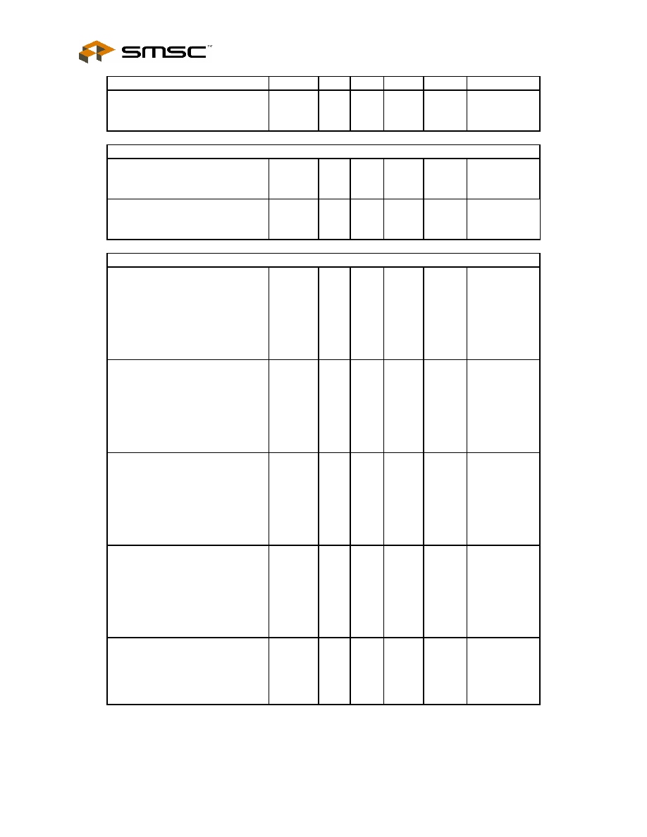
Non-PCI Single-Chip Full Duplex Ethernet Controller with Magic Packet
Rev. 09/10/2004
Page 94
SMSC LAN91C965v&3v
DATASHEET
PARAMETER
SYMBOL
MIN TYP MAX UNITS COMMENTS
ID Type Buffers
Input Current
I
IH
+50
+150
µA
V
IN
= V
CC
Input Current for V
cc
= 3.3V (Revisions E and later)
IP Type Buffers
Input Current
I
IL
-100
-50
µA
V
IN
= 0
ID Type Buffers
Input Current
I
IH
+50
+100
µA
V
IN
= V
CC
Output Voltage for V
cc
= 5.0V
I/O4 Type Buffer
Low Output Level
High Output Level
Output Leakage
V
OL
V
OH
I
LEAK
2.4
-10
0.4
+10
V
V
µA
I
OL
= 4 mA
I
OH
= -2 mA
V
IN
= 0 to V
CC
I/O24 Type Buffer
Low Output Level
High Output Level
Output Leakage
V
OL
V
OH
I
LEAK
2.4
-10
0.5
+10
V
V
µA
I
OL
= 24 mA
I
OH
= -12 mA
V
IN
= 0 to V
CC
O24 Type Buffer
Low Output Level
High Output Level
Output Leakage
V
OL
V
OH
I
LEAK
2.4
-10
0.5
+10
V
V
µA
I
OL
= 24 mA
I
OH
= -12 mA
V
IN
= 0 to V
CC
O4 Type Buffer
Low Output Level
High Output Level
Output Leakage
V
OL
V
OH
I
LEAK
2.4
-10
0.4
+10
V
V
A
I
OL
= 4 mA
I
OH
= -2 mA
V
IN
= 0 to V
CC
OD16 Type Buffer
Low Output Level
Output Leakage
V
OL
I
LEAK
-10
0.5
+10
V
µA
I
OL
= 16 mA
V
IN
= 0 to V
CC
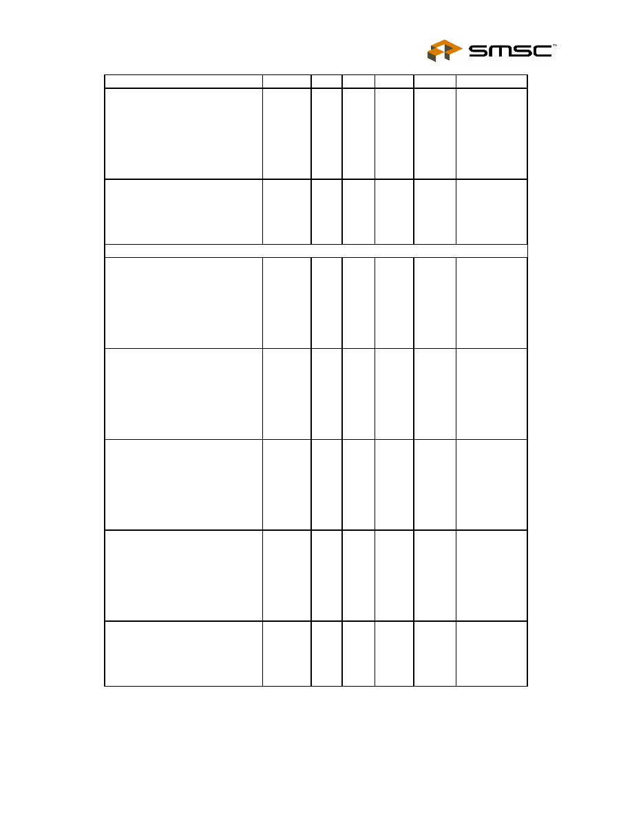
Non-PCI Single-Chip Full Duplex Ethernet Controller with Magic Packet
SMSC DS ≠ LAN91C965v&3v
Page 95
Rev. 09/10/2004
DATASHEET
PARAMETER
SYMBOL
MIN TYP MAX UNITS COMMENTS
O162 Type Buffer
Low Output Level
High Output Level
Output Leakage
V
OL
V
OH
I
LEAK
2.4
-10
0.5
+10
V
V
µA
I
OL
= 16 mA
I
OH
= -2 mA
V
IN
= 0 to V
CC
OD24 Type Buffer
Low Output Level
Output Leakage
V
OL
I
LEAK
-10
0.5
+10
V
µA
I
OL
= 24 mA
V
IN
= 0 to V
CC
Output Voltage for V
cc
= 3.3V (Revisions E and later)
I/O4 Type Buffer
Low Output Level
High Output Level
Output Leakage
V
OL
V
OH
I
LEAK
2.4
-10
0.4
+10
V
V
µA
I
OL
= 2 mA
I
OH
= -1 mA
V
IN
= 0 to V
CC
I/O24 Type Buffer
Low Output Level
High Output Level
Output Leakage
V
OL
V
OH
I
LEAK
2.4
-10
0.5
+10
V
V
µA
I
OL
= 16 mA
I
OH
= -6 mA
V
IN
= 0 to V
CC
O24 Type Buffer
Low Output Level
High Output Level
Output Leakage
V
OL
V
OH
I
LEAK
2.4
-10
0.5
+10
V
V
µA
I
OL
= 12 mA
I
OH
= -6 mA
V
IN
= 0 to V
CC
O4 Type Buffer
Low Output Level
High Output Level
Output Leakage
V
OL
V
OH
I
LEAK
2.4
-10
0.4
+10
V
V
µA
I
OL
= 2 mA
I
OH
= -1 mA
V
IN
= 0 to V
CC
OD16 Type Buffer
Low Output Level
Output Leakage
V
OL
I
LEAK
-10
0.5
+10
V
µA
I
OL
= 8 mA
V
IN
= 0 to V
CC
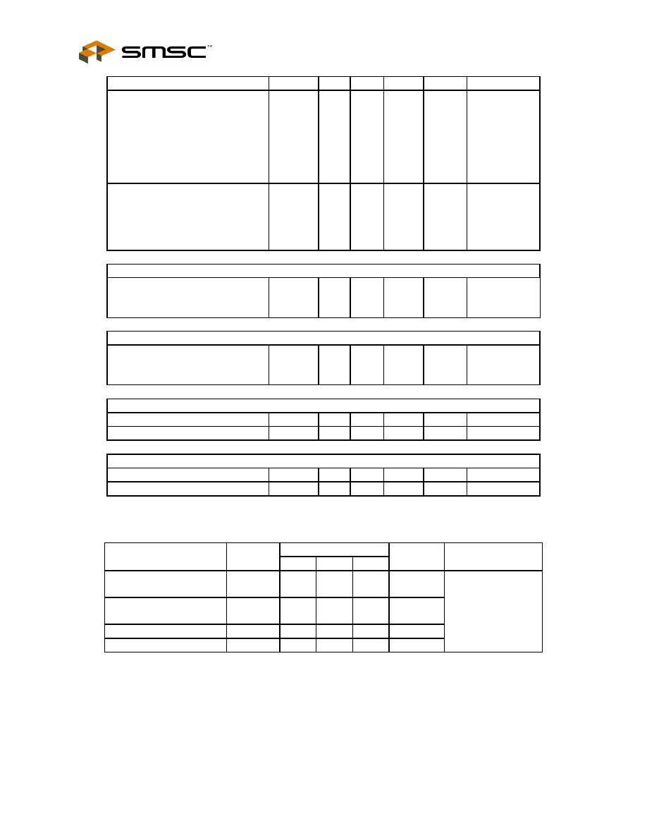
Non-PCI Single-Chip Full Duplex Ethernet Controller with Magic Packet
Rev. 09/10/2004
Page 96
SMSC LAN91C965v&3v
DATASHEET
PARAMETER
SYMBOL
MIN TYP MAX UNITS COMMENTS
O162 Type Buffer
Low Output Level
High Output Level
Output Leakage
V
OL
V
OH
I
LEAK
2.4
-10
0.5
+10
V
V
µA
I
OL
= 8 mA
I
OH
= -1 mA
V
IN
= 0 to V
CC
OD24 Type Buffer
Low Output Level
Output Leakage
V
OL
I
LEAK
-10
0.5
+10
V
µA
I
OL
= 12 mA
V
IN
= 0 to V
CC
Supply Current for V
cc
= 5.0V
Supply Current Active
Supply Current in power down mode
I
CC
I
Cdwn
50
8
95
mA
mA
All outputs
open.
Supply Current for V
cc
= 3.3V (Revisions E and later)
Supply Current Active
Supply Current in power down mode
I
CC
I
Cdwn
20
3
64
mA
mA
All outputs
open.
XTAL2 Output Drive for V
cc
= 5.0V
XTAL2 Output Drive High
I
CX2H
TBD
mA
XTAL2 Output Drive Low
I
CX2L
TBD
mA
XTAL2 Output Drive for V
cc
= 3.3V (Revisions E and later)
XTAL2 Output Drive High
I
CX2H
-6 mA
@2.4V
XTAL2 Output Drive Low
I
CX2L
3 mA
@0.4V
CAPACITANCE T
A
= 25
∞C; fc = 1MHz; V
CC
= 5V, or V
CC
= +3.3V for Revisions E and later
LIMITS
PARAMETER SYMBOL
MIN
TYP
MAX
UNIT
TEST
CONDITION
Clock Input Capacitance
(XTAL1)
C
CIN
5 6 pF
Clock Output Capacitance
(XTAL2)
C
COUT
5 6 pF
Input Capacitance
C
IN
10 pF
Output Capacitance
C
OUT
20 pF
All pins except pin
under test tied to AC
ground
Non-PCI Single-Chip Full Duplex Ethernet Controller with Magic Packet
SMSC DS ≠ LAN91C965v&3v
Page 97
Rev. 09/10/2004
DATASHEET
V
CC
= 5V +/- 10%
PARAMETER MIN
TYP
MAX
UNITS
10BASE-T
Receiver Threshold Voltage
100
mV
Receiver
Squelch
300 400 585 mV
Receiver Common Mode Range
0
V
DD
Transmitter Output: Voltage Source Resistance
±2
±2.5
±3
10
V
ohms
Transmitter Output DC Offset
50
mV
Transmitter Backswing Voltage to Idle
100
mV
Differential Input Voltage
±0.585
±3
V
AUI
Receiver Threshold Voltage
60
mV
Receiver
Squelch
180 240 300 mV
Receiver Common Mode Range
0
V
DD
Transmitter Output Voltage (R=78
)
±0.45 ±0.85 ±1.2
V
Transmitter Backswing Voltage to Idle
100
mV
Input Differential Voltage
±0.3
±1.2
V
Output Short Circuit (to V
CC
or GND) Current
±150
mA
Differential Idle Voltage (measured 8.0
µs after
last positive transition of data frame)
±40
mV

Non-PCI Single-Chip Full Duplex Ethernet Controller with Magic Packet
Rev. 09/10/2004
Page 98
SMSC LAN91C965v&3v
DATASHEET
V
CC
= 3.3V +/- 10% for Revisions E and later
PARAMETER MIN
TYP
MAX
UNITS
10BASE-T
Receiver Threshold Voltage
TBD
mV
Receiver
Squelch
225 260 520 mV
Receiver Common Mode Range
0
Vdd
Transmitter Output: Voltage Source Resistance
+/- 1.3
+/- 1.5
+/- 1.6
10
V
ohms
Transmitter Output DC Offset
50
mV
Transmitter Backswing Voltage to Idle
100
mV
Differential Input Voltage
+/- 0.520
+/- 3
V
AUI
Receiver Threshold Voltage
TBD
mV
Receiver
Squelch
120 140 160
mV
Receiver Common Mode Range
0
Vdd
Transmitter Output Voltage (R=78
)
+/- 0.39
+/- 0.47
+/- 0.55
V
Transmitter Backswing Voltage to Idle
100
mV
Input Differential Voltage
+/- 0.25
+/- 0.990
V
Output Short Circuit (to V
CC
or GND) Current
TBD
mA
Differential Idle Voltage (measured 8.0
µs after
last positive transition of data frame)
40
mV
CAPACITIVE LOAD ON OUTPUTS
nIOCS16,
IOCHRDY
240
pF
INTR0-3
120
pF
All other outputs
45 pF
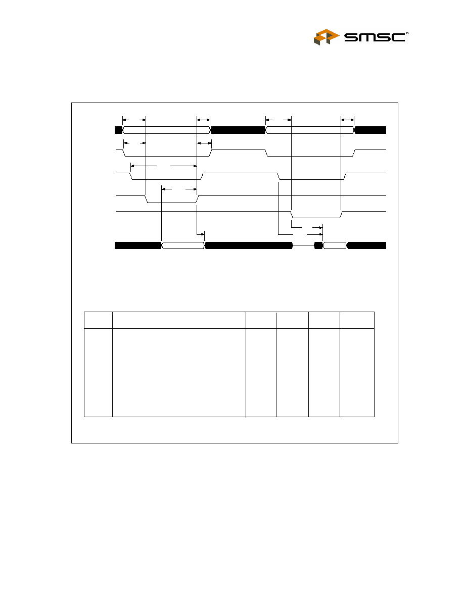
Non-PCI Single-Chip Full Duplex Ethernet Controller with Magic Packet
SMSC DS ≠ LAN91C965v&3v
Page 99
Rev. 09/10/2004
DATASHEET
Chapter 12 Timing Diagrams
Figure 12.1 ≠ Card Configuration Registers ≠ Read/Write PCMCIA Mode (A15=1)
ns
ns
ns
ns
ns
ns
ns
ns
ns
40
50
30
9
25
15
25
15
60
0
t57
t58
t59
t60
t61
t62
t63
t64
t65
Write Data Setup to nWE Rising
Write Data Hold after nWE Rising
nOE Low to Valid Data
Address, nREG Setup to nWE Active
Address, nREG Hold after nOE Inactive
Address, nREG Setup to nOE Active
Address, nREG Hold after Control Inactive
nCE1 Setup to nWE Rising
nCE1 Low to Valid Data
Parameter
min
typ
max
units
t60
t63
t62
t61
t60
t64
t57
t58
t59
t65
valid
valid
valid
valid
A0-9,A15
nREG
nCE1
nWE
nOE
D0-7
t63

Non-PCI Single-Chip Full Duplex Ethernet Controller with Magic Packet
Rev. 09/10/2004
Page 100
SMSC LAN91C965v&3v
DATASHEET
Figure 12.2 ≠ Local Bus Consecutive Read Cycles
BALE Tied High
VALID ADDRESS
VALID ADDRESS
t15
t4
t3
t20
t5
t6
Z
Z
A0-15
AEN, nSBHE
nIOCS16
nIORD
D0-15
t3
t4
t5
t6
t15
t20
Address, nSBHE, AEN Setup to Control Active
Address, nSBHE, AEN Hold after Control
Inactive
nIORD Low to Valid Data
nIORD High to Data Floating
A4-A15, AEN Low, BALE High to nIOCS16
Low
Cycle time*
Parameter
min
typ
max
units
10
20
185
25
15
12
ns
ns
ns
ns
ns
ns
IOCHRDY not used - t20 has to be met
*Note: The cycle time is defined only for consecutive accesses to the Data Register. These
values assume
that IOCHRDY is not used.
VALID DATA
OUT
VALID DATA
OUT
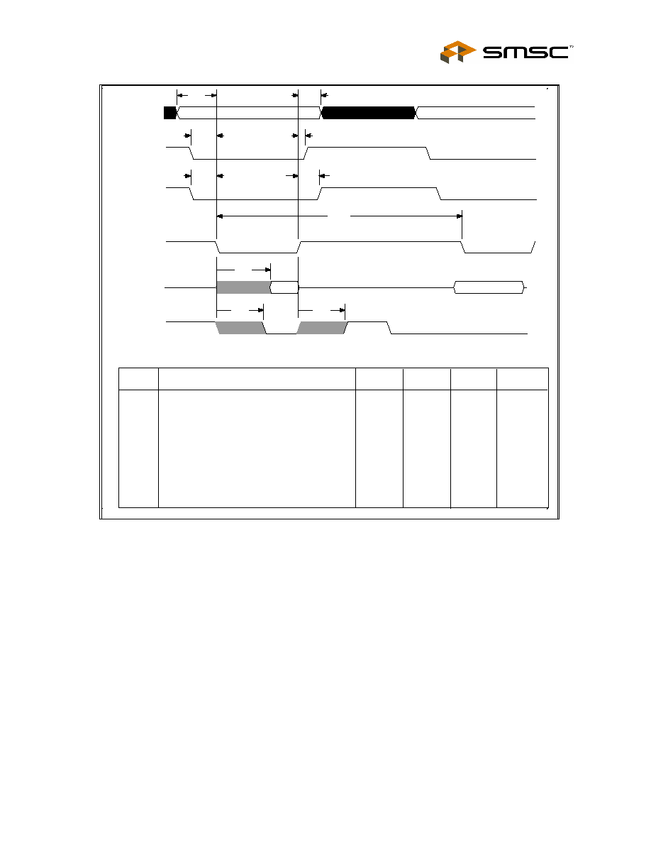
Non-PCI Single-Chip Full Duplex Ethernet Controller with Magic Packet
SMSC DS ≠ LAN91C965v&3v
Page 101
Rev. 09/10/2004
DATASHEET
Figure 12.3 - PCMCIA Consecutive Read Cycles
ns
ns
ns
ns
ns
ns
ns
ns
ns
35
40
0
5
5
185
0
15
25
15
0
Parameter
t46
t47
t48
t20
t49
t50
t51
t52
t53
nIORD to INPACK Delay
nREG Low to Control Active
nCE1,nCE2 Setup to Control Active
Cycle Time (No Wait States)
nREG Hold after Control Active
nCE1,nCE2 Hold after Control Inactive
Address Setup to Control Active
Address Hold after Control Inactive
nIORD Active to Data Valid
min
typ
max
units
t51
t52
t47
t49
t48
t50
t20
t53
t46
t46
valid
valid
A0-9,A15
nREG
nCE1,nCE2
nIORD
D0-15
nINPACK
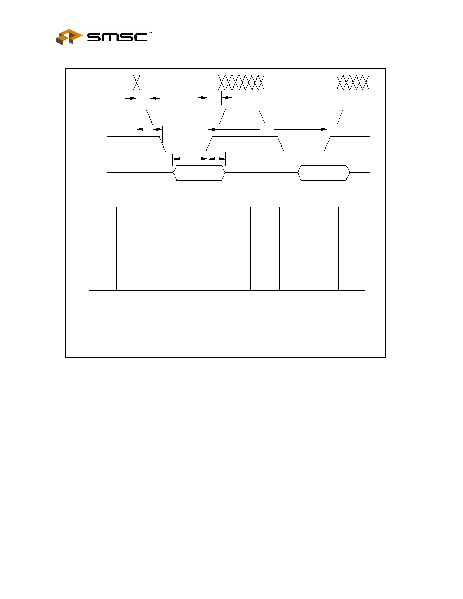
Non-PCI Single-Chip Full Duplex Ethernet Controller with Magic Packet
Rev. 09/10/2004
Page 102
SMSC LAN91C965v&3v
DATASHEET
Figure 12.4 ≠ Local Bus Consecutive Write Cycles
VALID ADDRESS
VALID ADDRESS
t15
t4
t3
t20
A0-15
AEN, nSBHE
nIOCS16
nIOWR
D0-15
VALID DATA IN
VALID DATA
t7
t8
BALE Tied High
t3
t4
t7
t8
t15
t20
12
ns
ns
ns
ns
ns
ns
Address, nSBHE, AEN Setup to Control Active
Address, nSBHE, AEN Hold after Control
Inactive
Data Setup to nIOWR Rising
Data Hold after nIOWR Rising
A4-A15, AEN Low, BALE High to nIOCS16
Low
Cycle time*
Parameter
min
typ
max
units
10
5
5
5
185
IOCHRDY not used - t20 has to be met
*Note: The cycle time is defined only for consecutive accesses to the Data Register. These values assume
that IOCHRDY is not used.
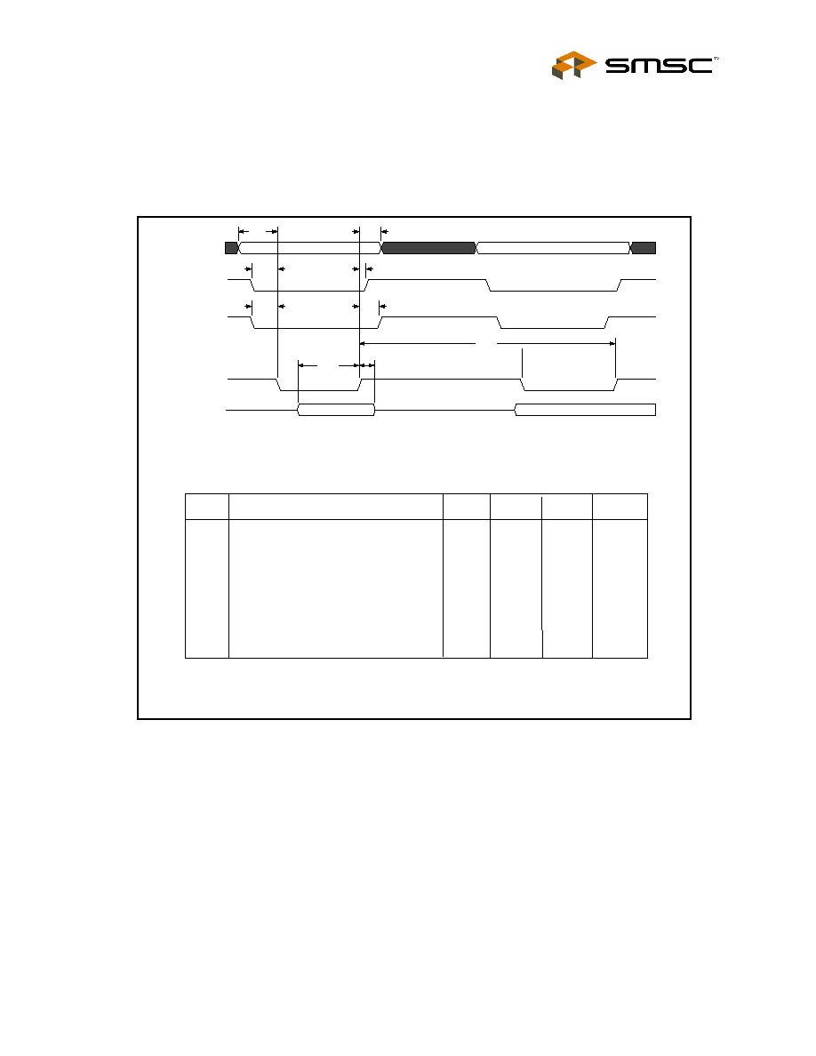
Non-PCI Single-Chip Full Duplex Ethernet Controller with Magic Packet
SMSC DS ≠ LAN91C965v&3v
Page 103
Rev. 09/10/2004
DATASHEET
Figure 12.5 - PCMCIA Consecutive Write Cycles
5
5
0
15
25
15
185
30
9
t51
t52
t47
t49
t48
t50
t20
t54
t55
valid
valid
A0-9,A15
nREG
nCE1,nCE2
nIOWR
D0-15
t47
t48
t49
t50
t51
t52
t20
t54
t55
ns
ns
ns
ns
ns
ns
ns
ns
ns
nREG Low Setup to Control Active
nCE1,nCE2 Setup to Control Active
nREG Hold after Control Inactive
nCE1,nCE2 Hold after Control Inactive
Address Setup to Control Active
Address Hold after Control Inactive
Cycle Time (No Wait States)
Write Data Setup to nIOWR Rising
Write Data Hold after nIOWR Rising
Parameter
min
typ
max
units
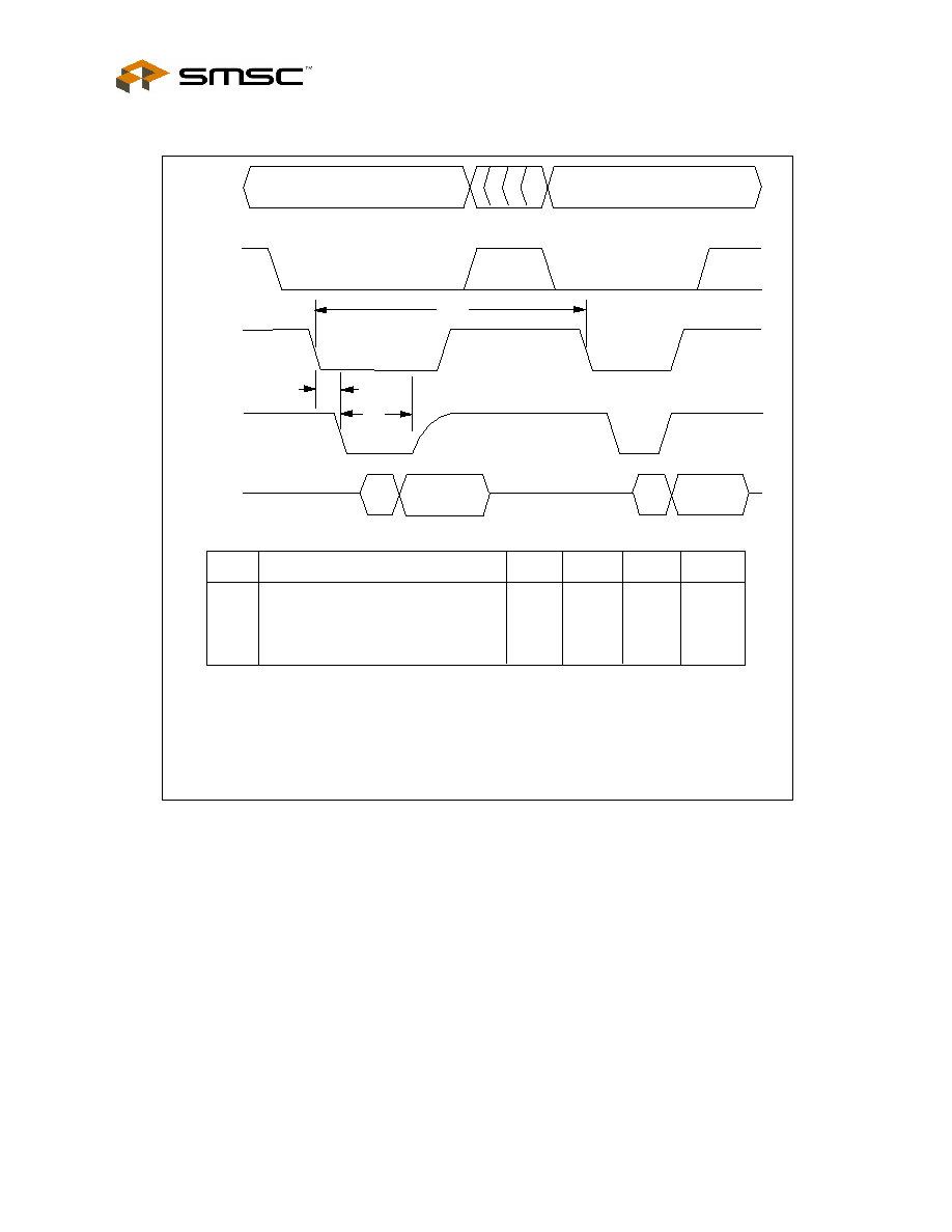
Non-PCI Single-Chip Full Duplex Ethernet Controller with Magic Packet
Rev. 09/10/2004
Page 104
SMSC LAN91C965v&3v
DATASHEET
Figure 12.6 ≠ Local Bus Consecutive Read and Write Cycles
t20
A0-15
AEN,
nSBHE
nIOCS16
nIOWR
D0-D15
VALID ADDRESS
VALID ADDRESS
nIORD
t9
t10
Z
Z
Z
VALID DATA
VALID DATA
IOCHRDY
Z
Z
Control Active to IOCHRDY Low
IOCHRDY Low Pulse Width*
Cycle time**
Parameter
min
typ
max
units
100
185
12
150
ns
ns
ns
t9
t10
t20
*Note: Assuming NO WAIT ST = 0 in configuration register and cycle time observed.
**Note: The cycle time is defined only for accesses to the Data Register as follows:
For Data Register Read - From nIORD falling to next nIORD falling
For Data Register Write - From nIOWR rising to next nIOWR rising

Non-PCI Single-Chip Full Duplex Ethernet Controller with Magic Packet
SMSC DS ≠ LAN91C965v&3v
Page 105
Rev. 09/10/2004
DATASHEET
Figure 12.7 ≠ Data Register Special Read Access
A0-15
(ISA)
AEN,
nSBHE
nIOCS16
D0-D15
nIORD
VALID DATA
VALID ADDRESS
IOCHRDY
OUT
t9
t18
t19
Z
Z
Parameter
min
typ
max
units
15
575
225
ns
ns
ns
t9
t18
t19
Control Active to IOCHRDY Low
IOCHRDY Width when Data is Unavailable at
Data Register
Valid Data to IOCHRDY Inactive
IOCHRDY is used instead of meeting t20 and t43.
"No Wait St' bit is 1 - IOCHRDY only negated if needed and only for Data Register access.
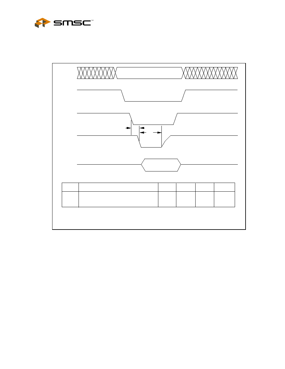
Non-PCI Single-Chip Full Duplex Ethernet Controller with Magic Packet
Rev. 09/10/2004
Page 106
SMSC LAN91C965v&3v
DATASHEET
Figure 12.8 ≠ Data Register Special Write Access
A0-15
(ISA)
AEN,
nSBHE
nIOCS16
D0-D15
nIOWR
VALID DATA IN
VALID ADDRESS
IOCHRDY
t18
Z
Z
Parameter
min
typ
max
units
15
425
t9
t18
Control Active to IOCHRDY Low
IOCHRDY Width when Data Register is Full
IOCHRDY is used instead of meeting t20 and t44.
'No Wait St' bit is 1 - IOCHRDY only negated if needed and only for Data Register access.
ns
ns
t9

Non-PCI Single-Chip Full Duplex Ethernet Controller with Magic Packet
SMSC DS ≠ LAN91C965v&3v
Page 107
Rev. 09/10/2004
DATASHEET
Figure 12.9 - 8-Bit Mode Register Cycles
A0-15
(ISA)
AEN
nIORD
D0-7
nIOWR
t3
t3
t5
Z
VALID DATA OUT
Z
VALID DATA IN
t7
t8
VALID ADDRESS
t3
t5
t7
t8
Address, nSBHE, AEN Setup to Control Active
nIORD Low to Valid Data
Data Setup to nIOWR Rising
Data Hold after nIOWR Rising
Parameter
min
typ
max
units
25
30
9
40
ns
ns
ns
ns
VALID ADDRESS
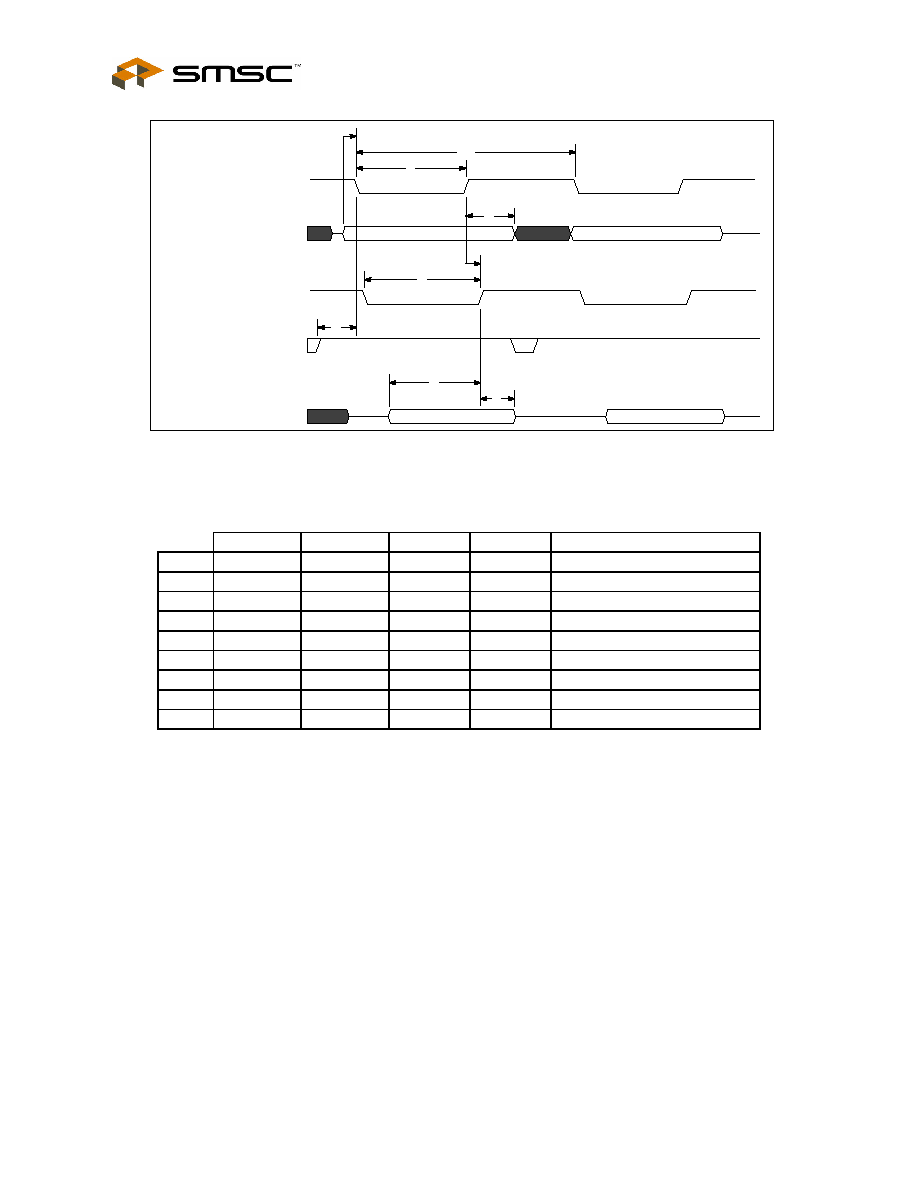
Non-PCI Single-Chip Full Duplex Ethernet Controller with Magic Packet
Rev. 09/10/2004
Page 108
SMSC LAN91C965v&3v
DATASHEET
Figure 12.10 - 68000 Read Timing
MIN TYP MAX
UNIT
COMMENTS
t1
0
nsec
R/nW asserted before nAS
t2
45
nsec
nAS assertion time
t3 15
nsec
Address
setup
time
t4
10
nsec
Address hold time
t5
0
nsec
nAS to xDS deassertion delay
t6
45
nsec
xDS assertion time
t7
10
nsec
Data setup time (Access time)
t9
0
30
nsec
Data hold time
t10
75
nsec
Consecutive reads cycle time
t10
t4
t2
t2
t3
nAS(nAEN)
ADD
t6
t6
t1
t5
xDS,LDS,UDS (nIORD)
R/nW(nIOWR)
t9
t7
DATA

Non-PCI Single-Chip Full Duplex Ethernet Controller with Magic Packet
SMSC DS ≠ LAN91C965v&3v
Page 109
Rev. 09/10/2004
DATASHEET
t10
t2
t2
t3
nAS (nAEN)
t4
t6
t7
t5
t7
ADD
xDS,LDS,UDS (nIORD)
t9
t1
t8
R/nW (nIOWR)
DATA
Figure 12.11 - 68000 Write Timing
MIN
TYP
MAX
UNIT
COMMENTS
t1
0
nsec
R/nW assertion before nAS
t2
30
nsec
nAS assertion time
t3 15 nsec
Address
setup
time
t4
10
nsec
Address hold time
t5
15
nsec
nAS to xDS
t6
0
nsec
xDS deassertion delay to nAS deassertion
t7
15
nsec
xDS assertion time
t8
10
nsec
Data setup time
t9
10
nsec
Data hold time
t10 60 nsec
Cycle
time
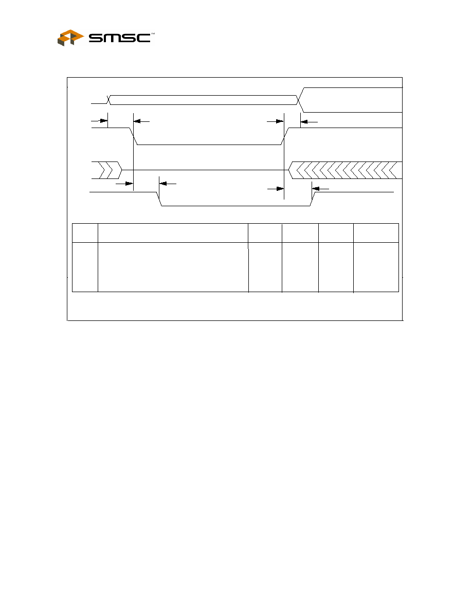
Non-PCI Single-Chip Full Duplex Ethernet Controller with Magic Packet
Rev. 09/10/2004
Page 110
SMSC LAN91C965v&3v
DATASHEET
Figure 12.12 ≠ External ROM Read Access
A0-19
nMEMRD
ADDRESS VALID
D0-15
t3
t4
Z
BALE tied high
t3
t4
t16
t17
Address Setup to Control Active
Address Hold after Control Inactive
nMEMRD Low to nROM Low(Internal)
nMEMRD High to nROM High(Internal)
Parameter
min
typ
max
units
10
20
0
0
20
35
ns
ns
ns
ns
t16
t17
nROM
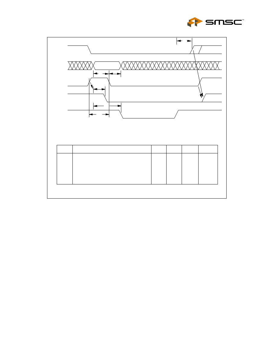
Non-PCI Single-Chip Full Duplex Ethernet Controller with Magic Packet
SMSC DS ≠ LAN91C965v&3v
Page 111
Rev. 09/10/2004
DATASHEET
Figure 12.13 ≠ Local Bus Register Access When Using Bale
AEN
nIOCS16
A0-15,
nSBHE
nIORD
BALE
nIOWR
t4
VALID
t1
t2
t15
t3
t1
t2
t3
t4
t15
Address, nSBHE Setup to BALE Falling
Address, nSBHE Hold after BALE Falling
Address, nSBHE, AEN Setup to Control Active
AEN Hold after Control Inactive
A4-A15, AEN Low, BALE High to nIOCS16 Low
Parameter
min
typ
max
units
12
ns
ns
ns
ns
ns
t4 not needed. nIOCS16 not relevant in 8-bit mode.
10
5
25
20
t5
t5
BALE Pulse Width
15
ns
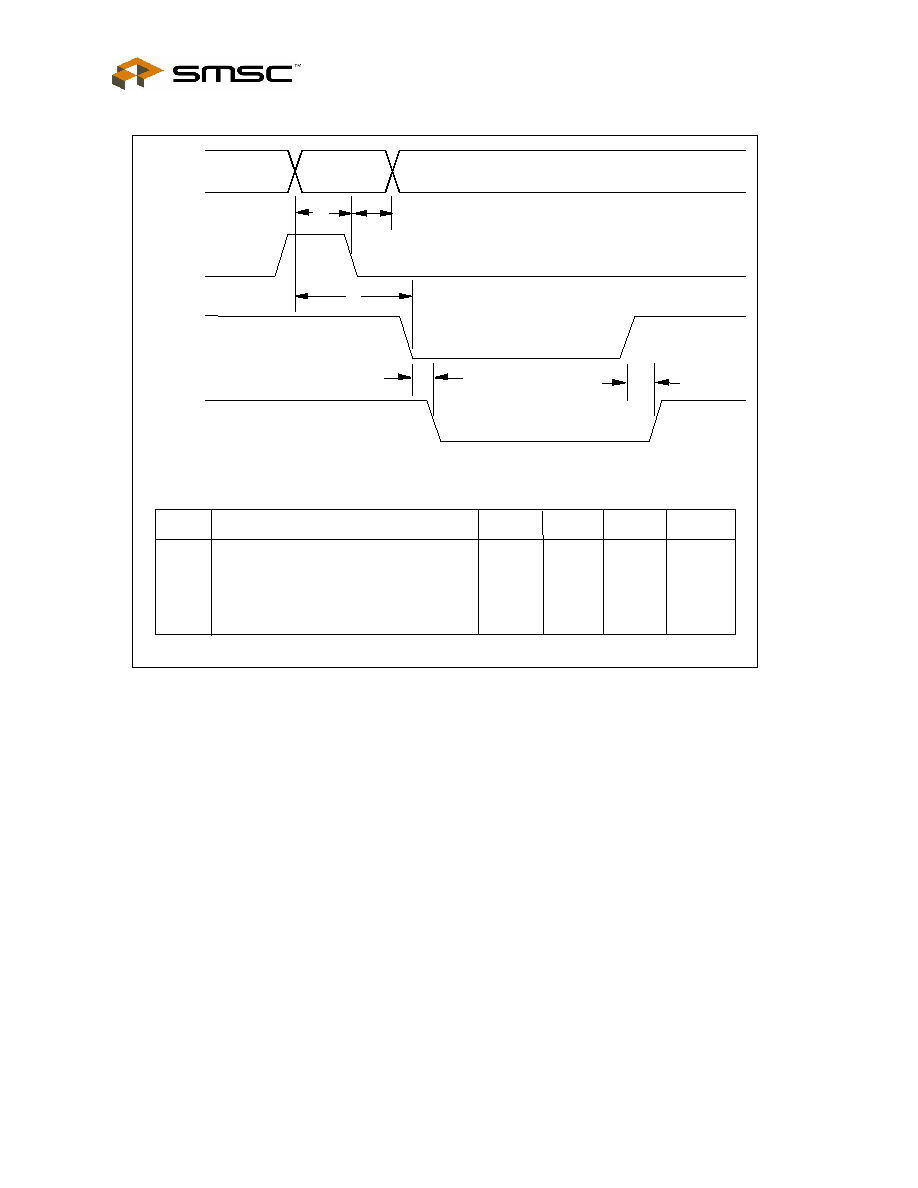
Non-PCI Single-Chip Full Duplex Ethernet Controller with Magic Packet
Rev. 09/10/2004
Page 112
SMSC LAN91C965v&3v
DATASHEET
Figure 12.14 ≠ External ROM Read Access Using Bale
Address Setup to BALE Falling
Address Hold after BALE Falling
Address Setup to Control Active
nMEMRD Low to nROM Low
nMEMRD High to nROM High
nMEMRD
A0-19
nROM
BALE
VALID
t1
t2
t3
t16
t17
t1
t2
t3
t16
t17
10
5
25
20
35
ns
ns
ns
ns
ns
Parameter
mi n
ty p
unit s
max
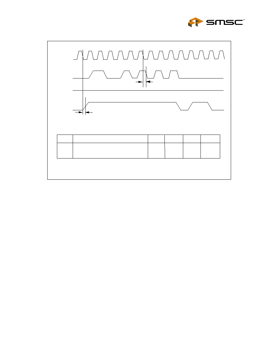
Non-PCI Single-Chip Full Duplex Ethernet Controller with Magic Packet
SMSC DS ≠ LAN91C965v&3v
Page 113
Rev. 09/10/2004
DATASHEET
Figure 12.15 - EEPROM Read
EEDI
EESK
EEDO
EECS
EESK Falling to EECS Changing
t21
Parameter
min
typ
max
units
15
ns
t21
0
9346 is typically the serial EEPROM used.
t68
t68
EESK Falling to EEDO Changing
25
ns
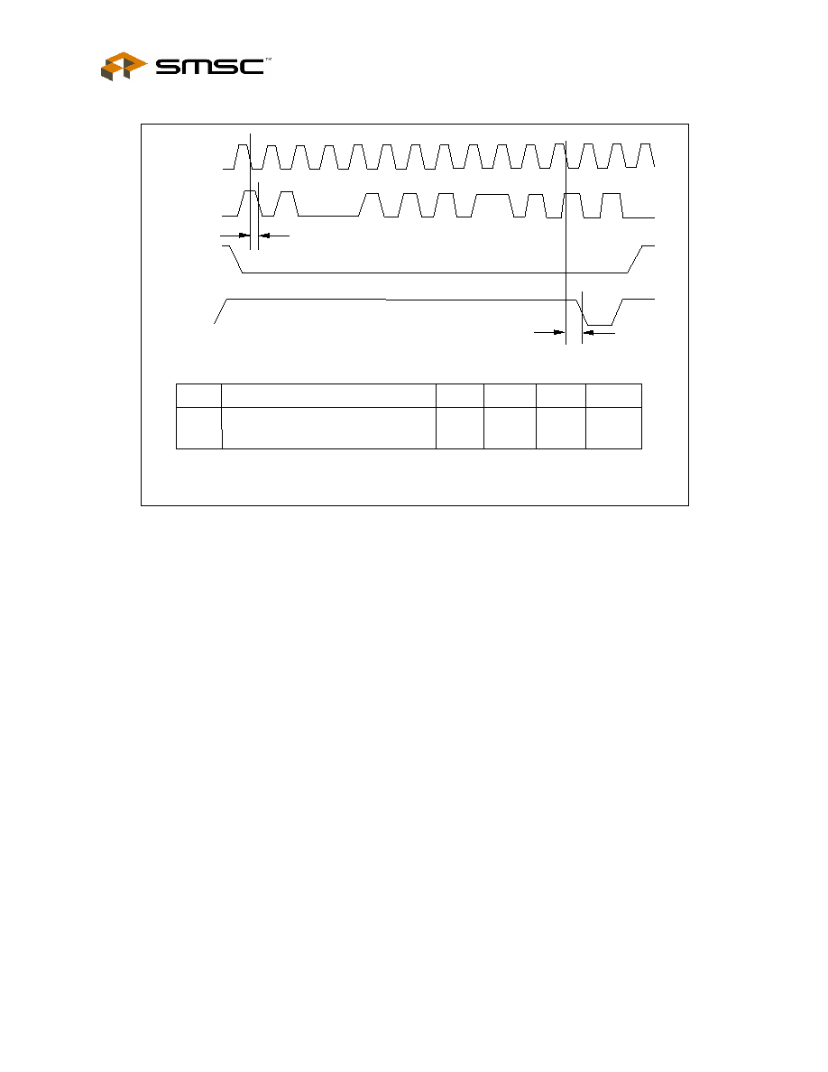
Non-PCI Single-Chip Full Duplex Ethernet Controller with Magic Packet
Rev. 09/10/2004
Page 114
SMSC LAN91C965v&3v
DATASHEET
Figure 12.16 - EEPROM Write
EESK
EEDO
EEDI
EECS
EESK Falling to EECS Changing
t69
Parameter
min
typ
max
units
5
ns
t69
9346 is typically the serial EEPROM used.
EESK Falling to EEDO Changing
t70
20
ns
t70

Non-PCI Single-Chip Full Duplex Ethernet Controller with Magic Packet
SMSC DS ≠ LAN91C965v&3v
Page 115
Rev. 09/10/2004
DATASHEET
ns
ns
20
25
nWE to nFWE Delay
Address, nREG, nCE1 Delay to nFCS
t66
t67
Parameter
min
typ
max
units
t67
t67
t67
t67
t67
t67
t67
t67
t67
t67
t67
t67
t66
t66
valid valid
A0-9,A15
nREG
nCE1
nFCS
nWE
nFWE
nOE
0
0
Figure 12.17 - PCMCIA Attribute Memory Read/Write (A15=0)
Figure 12.18 ≠ External ENDEC Interface ≠ Start of Transmit
nTXEN
TXD
TXCLK
t22
t22
t22
min
typ
max
unit
u
25
ns
0
Parameter
TXD, nTXEN Delay from TXCLK Falling
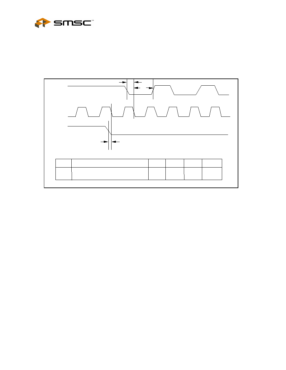
Non-PCI Single-Chip Full Duplex Ethernet Controller with Magic Packet
Rev. 09/10/2004
Page 116
SMSC LAN91C965v&3v
DATASHEET
Figure 12.19 ≠ External ENDEC Interface ≠ Receive Data
(RXD SAMPLED BY FALLING RXCLK)
RXD
RXCLK
nCRS
t23
t24
t23
nCRS, RXD Setup to RXCLK Falling
nCRS, RXD Hold after RXCLK Falling
t23
t24
Parameter
min
typ
max
units
ns
ns
10
30
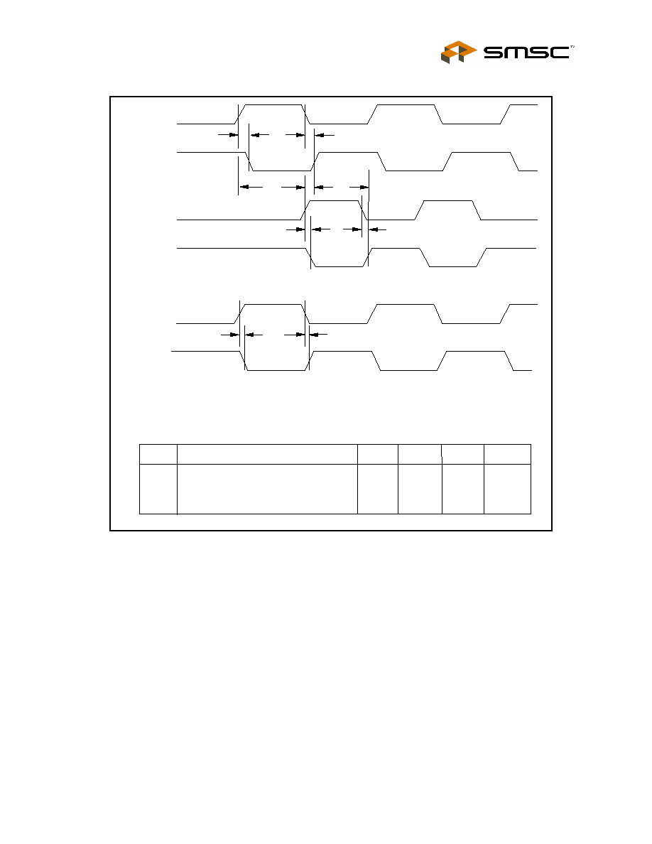
Non-PCI Single-Chip Full Duplex Ethernet Controller with Magic Packet
SMSC DS ≠ LAN91C965v&3v
Page 117
Rev. 09/10/2004
DATASHEET
Figure 12.20 ≠ Differential Output Signal Timing (10BASE-T and AUI)
TPETXP
TPETXN
TPETXDN
TPETXDP
TXP
TXN
t31
t32
t33
t34
TPETXP to TPETXN Skew
TPETXP(N) to TPETXDP(N) Delay
TPETXDN to TPETXDP Skew
TXP to TXN Skew
Parameter
min
typ
max
units
-1
47
-1
-1.5
+1
53
+1
1.5
ns
ns
ns
ns
t31
t31
t32
t32
t33
t33
t34
t34
TWISTED PAIR DRIVERS
AUI DRIVERS
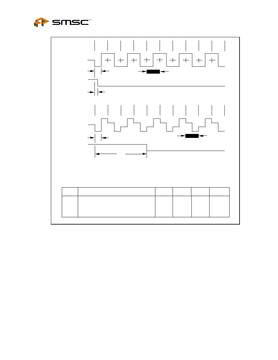
Non-PCI Single-Chip Full Duplex Ethernet Controller with Magic Packet
Rev. 09/10/2004
Page 118
SMSC LAN91C965v&3v
DATASHEET
Figure 12.21 ≠ Receive Timing ≠ Start of Frame (AUI and 10BASE-T)
1
1
0
1
1
0
1
0
1
0
0
first bit decoded
t35
t36
1
1
0
1
1
0
1
0
1
0
0
t37
first bit decoded
t38
RECP
RECN
nCRS
(internal)
TPERXP(N)
nCRS
(internal)
t35
t36
t37
t38
Noise Pulse Width Reject (AUI)
Carrier Sense Turn On Delay (AUI)
Noise Sense Pulse Width Reject (10BASE-T)
Carrier Sense Turn On Delay (10BASE-T)
Parameter
min
typ
max
units
15
50
15
450
30
100
30
550
ns
ns
ns
ns
25
70
25
500

Non-PCI Single-Chip Full Duplex Ethernet Controller with Magic Packet
SMSC DS ≠ LAN91C965v&3v
Page 119
Rev. 09/10/2004
DATASHEET
Figure 12.22 ≠ Receive Timing ≠ End of Frame (AUI and 10BASE-T)
b
a
1/0
last bit
TPERXP
TPERXN
RECP
RECN
nCRS
(internal)
t39
t39
Receiver Turn Off Delay
Parameter
min
typ
max
units
200
300
ns
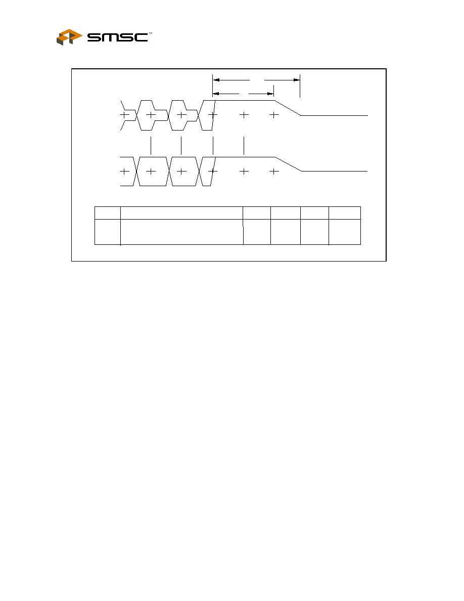
Non-PCI Single-Chip Full Duplex Ethernet Controller with Magic Packet
Rev. 09/10/2004
Page 120
SMSC LAN91C965v&3v
DATASHEET
Figure 12.23 ≠ Transmit Timing ≠ End of Frame (AUI and 10BASE-T)
b
a
1/0
last bit
TPETXP
TPETXN
TXP
TXN
t40
t41
Transmit Output High to Idle in Half-Step Mode
Transmit Output High before Idle in Half-Step
Mode
Parameter
min
typ
max
units
200
800
ns
ns
t40
t41
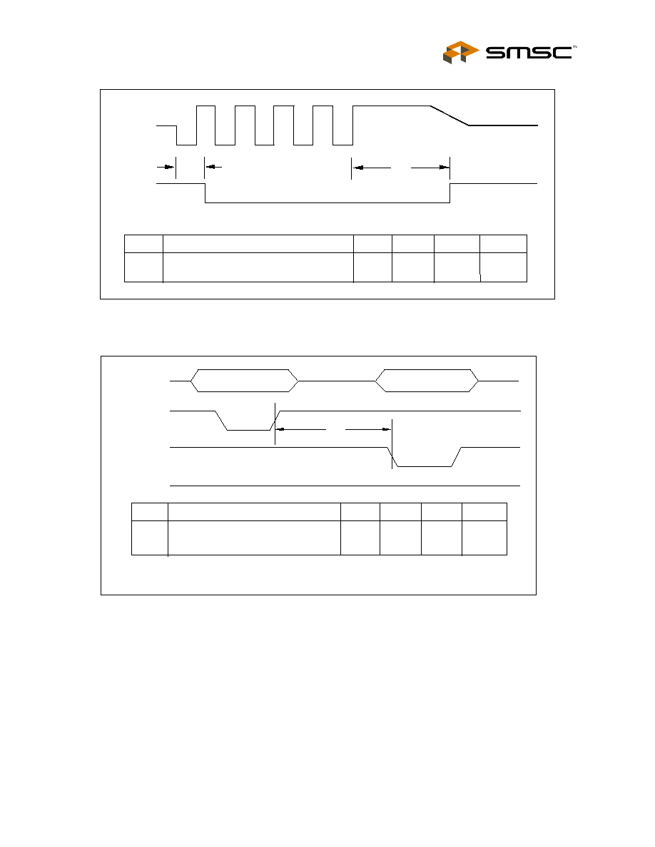
Non-PCI Single-Chip Full Duplex Ethernet Controller with Magic Packet
SMSC DS ≠ LAN91C965v&3v
Page 121
Rev. 09/10/2004
DATASHEET
COLLP
COLLN
t42
t43
COL
(internal)
t42
t43
Collision Turn On Delay
Collision Turn Off Delay
Parameter
min
typ
max
units
50
350
ns
ns
Figure 12.24 ≠ Collision Timing (AUI)
Figure 12.25 ≠ Memory Read Timing
ADDRESS
POINTER
REGISTER
DATA
REGISTER
nIOWR
nIORD
IOCHRDY/
nWAIT (Z)
t44
t44
Pointer Register Reloaded to a Word of Data
Prefetched into Data Register
Parameter
min
typ
max
units
ns
2 * t20
Note: If t44 is not met, IOCHRDY will be negated for the required time. This parameter can be ignored if
IOCHRDY is connected to the system.
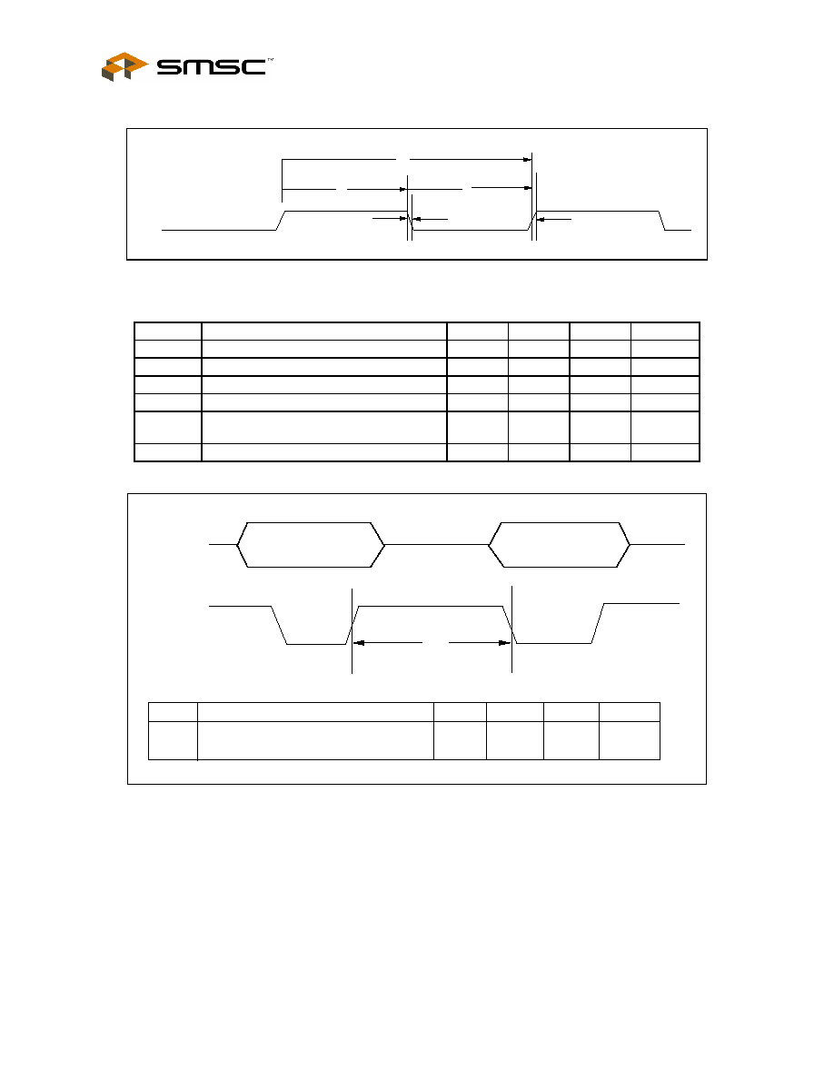
Non-PCI Single-Chip Full Duplex Ethernet Controller with Magic Packet
Rev. 09/10/2004
Page 122
SMSC LAN91C965v&3v
DATASHEET
CLOCK
t 2
t 2
t 1
t R
t F
Figure 12.26 ≠ Input Clock Timing
NAME DESCRIPTION MIN
TYP
MAX
UNITS
t1
Clock Cycle Time for 20 MHz
50
ns
t2
Clock High Time/Low Time for 20 MHz
30/20
20/30
ns
tR, tF
Clock Rise Time/Fall Time
5
ns
Xtal1 Startup time (from 1.6v of Vcc rising)
50
msec
Xtal1 Capture Range (Xtal1 frequency
variation)
19.7
20.3 MHz
Xtal Internal feedback resistor
1
3
Meg Ohm
ADDRESS
DATA
REGISTER
POINTER
REGISTER
nIOWR
t45
t45
Last Access to Data Register to Pointer
Reloaded
Parameter
min
typ
max
units
ns
2 * t20
Figure 12.27 ≠ Memory Write Timing
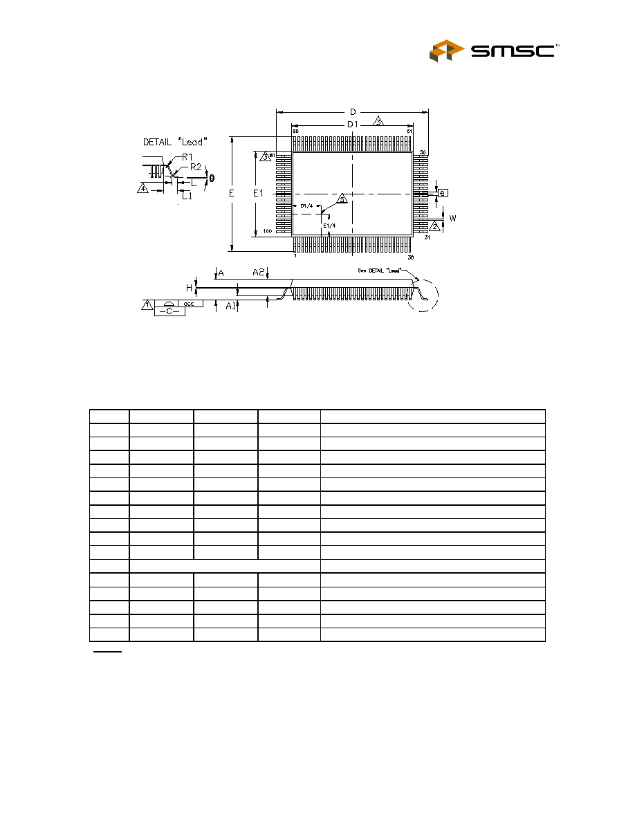
Non-PCI Single-Chip Full Duplex Ethernet Controller with Magic Packet
SMSC DS ≠ LAN91C965v&3v
Page 123
Rev. 09/10/2004
DATASHEET
Figure 12.28 - 100 PIN QFP Package
MIN
NOMINAL
MAX
REMARKS
A
~
~
3.4
Overall Package Height
A1
0.05 ~ 0.5
Standoff
A2
2.55 ~ 3.05
Body
Thickness
D
23.65 ~ 24.15
X
Span
D1
19.90
~
20.10
X body Size
E
17.65 ~ 18.15
Y
Span
E1
13.90
~
14.10
Y body Size
H
0.11
~
0.23
Lead Frame Thickness
L
0.73
0.88
1.03
Lead Foot Length
L1
~ 1.95 ~
Lead
Length
e
0.65 Basic
Lead Pitch
0
o
~ 7
o
Lead Foot Angle
W
0.20 ~ 0.40
Lead
Width
R1
0.10
~
0.25
Lead Shoulder Radius
R2
0.15
~
0.40
Lead Foot Radius
ccc
~ ~
0.10
Coplanarity
Notes:
1
Controlling Unit: millimeter.
2
Tolerance on the true position of the leads is ± 0.065 mm maximum
3
Package body dimensions D1 and E1 do not include the mold protrusion.
Maximum mold protrusion is 0.25 mm.
4
Dimension for foot length L measured at the gauge plane 0.25 mm above the seating plane.
5
Details of pin 1 identifier are optional but must be located within the zone indicated.
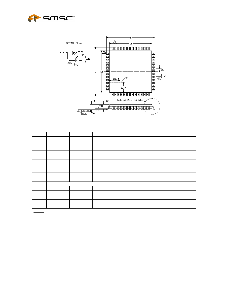
Non-PCI Single-Chip Full Duplex Ethernet Controller with Magic Packet
Rev. 09/10/2004
Page 124
SMSC LAN91C965v&3v
DATASHEET
Figure 12.29 - 100 PIN TQFP Package
MIN
NOMINAL
MAX
REMARKS
A
~
~
1.20
Overall Package Height
A1
0.05 ~ 0.15
Standoff
A2
0.95 ~ 1.05
Body
Thickness
D
15.80 ~ 16.20
X
Span
D1
13.90
~
14.10
X body Size
E
15.80 ~ 16.20
Y
Span
E1
13.90
~
14.10
Y body Size
H
0.09
~
0.20
Lead Frame Thickness
L
0.45
0.60
0.75
Lead Foot Length
L1
~ 1.00 ~
Lead
Length
e
0.50 Basic
Lead Pitch
0
o
~ 7
o
Lead Foot Angle
W
0.17 0.22 0.27
Lead
Width
R1
0.08
~
~
Lead Shoulder Radius
R2
0.08
~
0.20
Lead Foot Radius
ccc
~ ~
0.08
Coplanarity
Notes:
1
Controlling Unit: millimeter.
2
Tolerance on the true position of the leads is ± 0.04 mm maximum.
3
Package body dimensions D1 and E1 do not include the mold protrusion.
Maximum mold protrusion is 0.25 mm.
4
Dimension for foot length L measured at the gauge plane 0.25 mm above the seating plane.
5
Details of pin 1 identifier are optional but must be located within the zone indicated.

Non-PCI Single-Chip Full Duplex Ethernet Controller with Magic Packet
SMSC DS ≠ LAN91C965v&3v
Page 125
Rev. 09/10/2004
DATASHEET
Chapter 13 LAN91C96 Revisions
PAGE(S) SECTION/FIGURE/ENTRY
CORRECTION
DATE
REVISED
2
Ordering Information
Added lead-free ordering information
09/10/04
92
DC Electrical Characteristics
Modified Supply Current in power down
mode
08/11/04
65
Theory of Operation (Magic Packet
Support section)
Modified descriptions of Magic Packet
Support
08/11/04
50
I/O Space ≠ Bank1 Offset 2
Modified I/O base address 300h
decoding
09/30/02
124~125
Fig.12.28100 pin QFP Package;
Fig.12.28100 Pin TQFP Package;
Updated Pin Package diagrams
09/17/02
16
Chapter 4 Description of Pin
Functions
Add description of RBIAS pin
07/01/02
58
IO Space Bank 2 Offset 2 ≠ Interrupt
Modified the description of Interrupt
Registers
07/01/02
61
Figure 7.1 ≠ Interrupt Structure
Modified Interrupt Structure Figure
07/01/02
59
Bank 3 Offset A ≠ Revision Register
Changed the REV ID to 9
07/01/02
67
8.1, 8.2 Typical Flow of Events for
Transmit
Modified the flow chart
07/01/02
1
Title and document
Non-PCI replaces ISA/PCMCIA in title.
Local Bus replaces ISA throughout
document.
04/15/02
70
Figure 8.1 ≠ Interrupt Service Routine Figure has been updated.
04/15/02
37
Figure 6.1 ≠ Data Frame Format
Max Offset changed to 1534 from 1536
07/27/01
37
Data area in ram
Number of Bytes in Data Area changed
to 1531 from 2034
07/27/01
25
Figure 7
Update Figure 7
07/27/01
108
DC Electrical Characteristics
Update 3.3V Characteristic Numbers
replace TBD
07/27/01
80
Figure 15
Updated figure 15
03/21/01
37
Figure 6.1 ≠ Data Frame Format
Max Offset changed to 1534 from 1536
07/27/01
37
Data area in ram
Number of Bytes in Data Area changed
to 1531 from 2034
07/27/01
25
Figure 7
Update Figure 7
07/27/01
108
DC Electrical Characteristics
Update 3.3V Characteristic Numbers
replace TBD
07/27/01
80
Figure 15
Updated figure 15
03/21/01
55
I/O Space ≠ Bank 2/ Top of RX FIFO
Packet Number
MMU Commands changed from 3, 4 to
6, 8
See italicized text
07/18/00
20
Buffer Symbols
See italicized text
06/29/00
92
DC Electrical Characteristics
Updated table ≠ see italicized text
06/29/00
99
Timing Diagrams
Figures: 20-23, 25, 29, 31-33, 35-37
06/29/00