
SMSC LPC47M260
PRODUCT PREVIEW
Revision 0.2 (05-12-03)
Data Brief
Product Features
LPC47M260
LPC Super I/O with X-Bus Flash
Interface and Hardware Monitoring
Block
3.3 Volt Operation (SIO Block is 5 Volt Tolerant)
Low Pin Count (LPC) Interface
ACPI 2.0 Compliant
Programmable Wake-up Event Interface
PC99, PC2001 Compliant
X-Bus Flash Interface
-- 8-bit data transfers
-- Support for up to 1MByte (8Mbit) flash
-- Interfaces with 3V or 5V memory devices
-- Provides FWH and LPC Flash Emulation
Fan Control
-- Fan Speed Control Outputs (3)
-- Fan Tachometer Inputs (3)
Dual Game Port Interface
MPU-401 MIDI Support
General Purpose Input/Output Pins (27)
ISA Plug-and-Play Compatible Register Set
System Management Interrupt
Intruder Detection Support
Security Key Register (32 byte) for Device
Authentication
Watchdog Timer
LED Control (2)
2.88MB Super I/O Floppy Disk Controller
-- Licensed CMOS 765B Floppy Disk Controller
-- Software and Register Compatible with SMSC's
Proprietary 82077AACompatible Core
-- Supports Two Floppy Drives
-- Configurable Open Drain/Push-Pull Output Drivers
-- Supports Vertical Recording Format
-- 16-Byte Data FIFO
-- 100% IBM� Compatibility
-- Detects All Overrun and Underrun Conditions
-- Sophisticated Power Control Circuitry (PCC) Including
Multiple Powerdown Modes for Reduced Power
Consumption
-- DMA Enable Logic
-- Data Rate and Drive Control Registers
-- 480 Address, Up to Eight IRQ and Three DMA Options
Enhanced Digital Data Separator
-- 2 Mbps, 1 Mbps, 500 Kbps, 300 Kbps, 250 Kbps Data
Rates
-- Programmable Precompensation Modes
Serial Ports
-- Two Full Function Serial Ports
-- High Speed NS16C550A Compatible UARTs with
Send/Receive 16-Byte FIFOs
-- Supports 230k and 460k Baud
-- Programmable Baud Rate Generator
-- Modem Control Circuitry
-- 480 Address and 15 IRQ Options
Infrared Port
-- Multiprotocol Infrared Interface
-- IrDA 1.0 Compliant
-- SHARP ASK IR
-- 480 Addresses, Up to 15 IRQ
Multi-ModeTM Parallel Port with ChiProtectTM
-- Standard Mode IBM PC/XT
�,
PC/AT
�
, and PS/2TM
Compatible Bi-directional Parallel Port
-- Enhanced Parallel Port (EPP) Compatible
-- EPP 1.7 and EPP 1.9 (IEEE 1284 Compliant)
-- IEEE 1284 Compliant Enhanced Capabilities Port
(ECP)
-- ChiProtect Circuitry for Protection
-- 960 Address, Up to 15 IRQ and Three DMA Options
LPC Interface
-- Multiplexed Command, Address and Data Bus
-- Serial IRQ Interface Compatible with Serialized IRQ
Support for PCI Systems
-- PME Interface
Hardware Monitor
-- Low Pin Count (LPC) Interface
-- Monitor Power supplies (+5V, +12V, Vccp (processor
voltage), HVCC, VTR and VBAT)
-- Remote Thermal Sensing for Three External
Temperature Measurements
-- Internal Ambient Temperature Measurement
-- Limit Comparison of all Monitored Values
-- THERM# Pin for out-of-limit Temperature or Voltage
Indication
-- RESET# Pin for generating 20msec Low Reset Pulse
-- Configurable offset for internal or external temperature
channels.
128 Pin QFP, 3.2mm footprint Package

� STANDARD MICROSYSTEMS CORPORATION (SMSC) 2003
80 Arkay Drive
Hauppauge, NY 11788
(631) 435-6000
FAX (631) 273-3123
Standard Microsystems and SMSC are registered trademarks of Standard Microsystems Corporation. Product names and company names are the
trademarks of their respective holders. Circuit diagrams utilizing SMSC products are included as a means of illustrating typical applications; conse-
quently complete information sufficient for construction purposes is not necessarily given. Although the information has been checked and is believed
to be accurate, no responsibility is assumed for inaccuracies. SMSC reserves the right to make changes to specifications and product descriptions
at any time without notice. Contact your local SMSC sales office to obtain the latest specifications before placing your product order. The provision of
this information does not convey to the purchaser of the semiconductor devices described any licenses under the patent rights of SMSC or others.
All sales are expressly conditional on your agreement to the terms and conditions of the most recently dated version of SMSC's standard Terms of
Sale Agreement dated before the date of your order (the "Terms of Sale Agreement"). The product may contain design defects or errors known as
anomalies which may cause the product's functions to deviate from published specifications. Anomaly sheets are available upon request. SMSC
products are not designed, intended, authorized or warranted for use in any life support or other application where product failure could cause or
contribute to personal injury or severe property damage. Any and all such uses without prior written approval of an Officer of SMSC and further testing
and/or modification will be fully at the risk of the customer. Copies of this document or other SMSC literature, as well as the Terms of Sale Agreement,
may be obtained by visiting SMSC's website at http://www.smsc.com.
SMSC DISCLAIMS AND EXCLUDES ANY AND ALL WARRANTIES, INCLUDING WITHOUT LIMITATION ANY AND ALL IMPLIED WARRANTIES
OF MERCHANTABILITY, FITNESS FOR A PARTICULAR PURPOSE, TITLE, AND AGAINST INFRINGEMENT AND THE LIKE, AND ANY AND
ALL WARRANTIES ARISING FROM ANY COURSE OF DEALING OR USAGE OF TRADE.
IN NO EVENT SHALL SMSC BE LIABLE FOR ANY DIRECT, INCIDENTAL, INDIRECT, SPECIAL, PUNITIVE, OR CONSEQUENTIAL DAMAGES,
OR FOR LOST DATA, PROFITS, SAVINGS OR REVENUES OF ANY KIND; REGARDLESS OF THE FORM OF ACTION, WHETHER BASED ON
CONTRACT, TORT, NEGLIGENCE OF SMSC OR OTHERS, STRICT LIABILITY, BREACH OF WARRANTY, OR OTHERWISE; WHETHER OR NOT
ANY REMEDY IS HELD TO HAVE FAILED OF ITS ESSENTIAL PURPOSE; AND WHETHER OR NOT SMSC HAS BEEN ADVISED OF THE
POSSIBILITY OF SUCH DAMAGES.
ORDERING INFORMATION
Order Number(s):
LPC47M260-NR for 128 pin QFP package (3.2mm footprint)
Revision 0.2 (05-12-03)
2
SMSC LPC47M260
PRODUCT PREVIEW

SMSC LPC47M260
3
Revision 0.2 (05-12-03)
PRODUCT PREVIEW
General Description
The LPC47M260 is a 3.3V (Super I/O Block is 5V tolerant) PC99/PC2001 compliant Super I/O controller
with a Low Pin Count (LPC) interface. The LPC47M260 also includes Hardware Monitoring capabilities,
an X-Bus interface and enhanced Security features.
The X-Bus Flash Interface supports up to a 1MByte (8Mbit) flash device and provides both LPC and
firmware hub (FWH) emulation.
The LPC47M260's hardware monitoring capability includes voltage and temperature monitoring with the
ability to alert the system of out-of-limit conditions. There are 3 analog inputs for monitoring external
voltages of +5V, +12V and Vccp (core processor voltage), as well as internal monitoring of the devices
own HVCC, VTR and VBAT. The LPC47M260 includes support for monitoring two external temperatures
via thermisor inputs, one external temperature via a thermal diode input and an internal sensor for
measuring ambient temperature. The nTHERM pin is implemented to indicate out-of-limit temperature
and voltage conditions. The block has the ability to generate an 20ms low pulse via the nRESET pin.
The hardware monitoring block of the LPC47M260 is accessible via the LPC interface.
The LPC47M260 incorporates legacy Super I/O functionality including an IEEE 1284, EPP, and ECP
compatible parallel port, two serial ports that are 16C550A UART compatible, two IrDA 1.0 infrared ports,
and a floppy disk controller with SMSC's true CMOS 765B core and enhanced digital data separator,
The true CMOS 765B core provides 100% compatibility with IBM PC/XT and PC/AT architectures and
is software and register compatible with SMSC's proprietary 82077AA core.
The LPC47M260 provides other system related functionality that offers flexibility to the system designer,
including (27) General Purpose I/O control functions, an MPU-401 MIDI interface, control of two LED's
and a game port interface supporting two joysticks. The part also provides fan control using pulse width
modulator (PWM) outputs and fan tachometer inputs.
The LPC47M260 is ACPI 1.0/2.0 compatible and therefore supports multiple low power-down modes.
It incorporates sophisticated power control circuitry (PCC), which includes several wake-up events.
The LPC47M260 supports the ISA Plug-and-Play Standard register set (Version 1.0a). The I/O Address,
DMA Channel and hardware IRQ of each logical device in the LPC47M260 may be reprogrammed
through the internal configuration registers. There are up to 480 (960 - Parallel Port) I/O address
location options, a Serialized IRQ interface, and Three DMA channels.
Revision 0.2 (05-12-03)
4
SMSC LPC47M260
PRODUCT PREVIEW
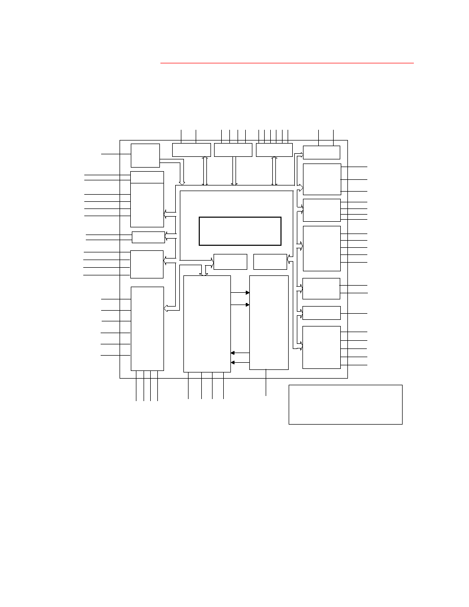
Block Diagram
Figure 1 LPC47M260 Block Diagram
FA
N
2
*
J
1
X
,
J1Y
*
IRTX2
*
IRR
X
2*
LPC47M260
(128 QFP)
DIGITAL DATA
SEPARATOR
WITH WRITE
PRECOM-
PENSATION
SMC PROPRIETARY
82077 COMPATIBLE
VERTICAL
FLOPPYDISK
CONTROLLER CORE
WDATA
WCLOCK
RCLOCK
RDATA
Game Port
Fan Control
2nd Infrared Port
F
A
N_
T
ACH
2*
F
A
N_
T
ACH
1*
FA
N
1
*
J
2
B1
, J2
B2
*
J
1
B1
, J1
B2
*
J
2
X
,
J2Y
*
LEDs
LE
D
2
*
LE
D
1
*
Internal Bus (Data, Address, and Control Lines)
Power Mgmt
nIO_PME*
nIO_SMI*
General
Purpose
I/O
GP1[0:7]*
GP2[1:2,5:7]*
GP3[2:5]*, GP40*, GP42*
GP5[0:7]*
R
DAT
A
,
WD
AT
A
DI
R,
ST
EP
,
DSK
CHG
,
DS0
,
DS1
*
M
T
R0
, M
T
R1
*
,
T
R
K
0
,
I
NDE
X,
WRT
P
RT
DR
VDEN
0
*
,
D
R
VD
EN1
*
W
G
AT
E
,
HD
S
E
L
Note 1: This diagram does not show power and ground
connections.
Note 2: Functions with "*" are located on multifunctional pins.
This diagram is designed to show the various functions
available on the chip (not pin layout).
Hardware
Monitoring
CLOCK
GEN
CLOCKI
LAD[3:0]
LFRAME#
LDRQ#
PCI_RESET#
SER_IRQ
PCI_CLK
LPC
Bus Interface
SERIAL
IRQ
RESET#/THERM#
Vccp_IN
+12V_IN
+5V_IN
HVSS
HVCC
TE
MP
_I
N
2
TE
M
P
_I
N
1
D0
+
D0
-
FA
N
3
*
F
A
N_
T
ACH
3*
WDT
Intruder
Detection
nINTRD_IN
32 Byte
Security Key
Register
Multi-Mode
Parallel Port
with
ChiProtect
TM
/
FDC MUX
PD[7,0]
BUSY, SLCT, PE,
ERROR, ACK
STROBE, INIT, SLCTIN,
ALF
High-Speed
16550A
UART
PORT 1
TXD1, RXD1
DSR1, DTR1
CTS1, RTS1
DCD1, RI1
High-Speed
16550A
UART
PORT 2
TXD2 (IRTX)*,
RXD2 (IRRX)*
DSR2*, DTR2*
DCD2*, RI2*
CTS2*, RTS2 *
MPU-401
Serial Port
X-Bus
Interface
MIDI_IN*
MIDI_OUT*
XA[19:0]
XD[7:0]
nXRD
nXWR
nXCS
SMSC LPC47M260
5
Revision 0.2 (05-12-03)
PRODUCT PREVIEW
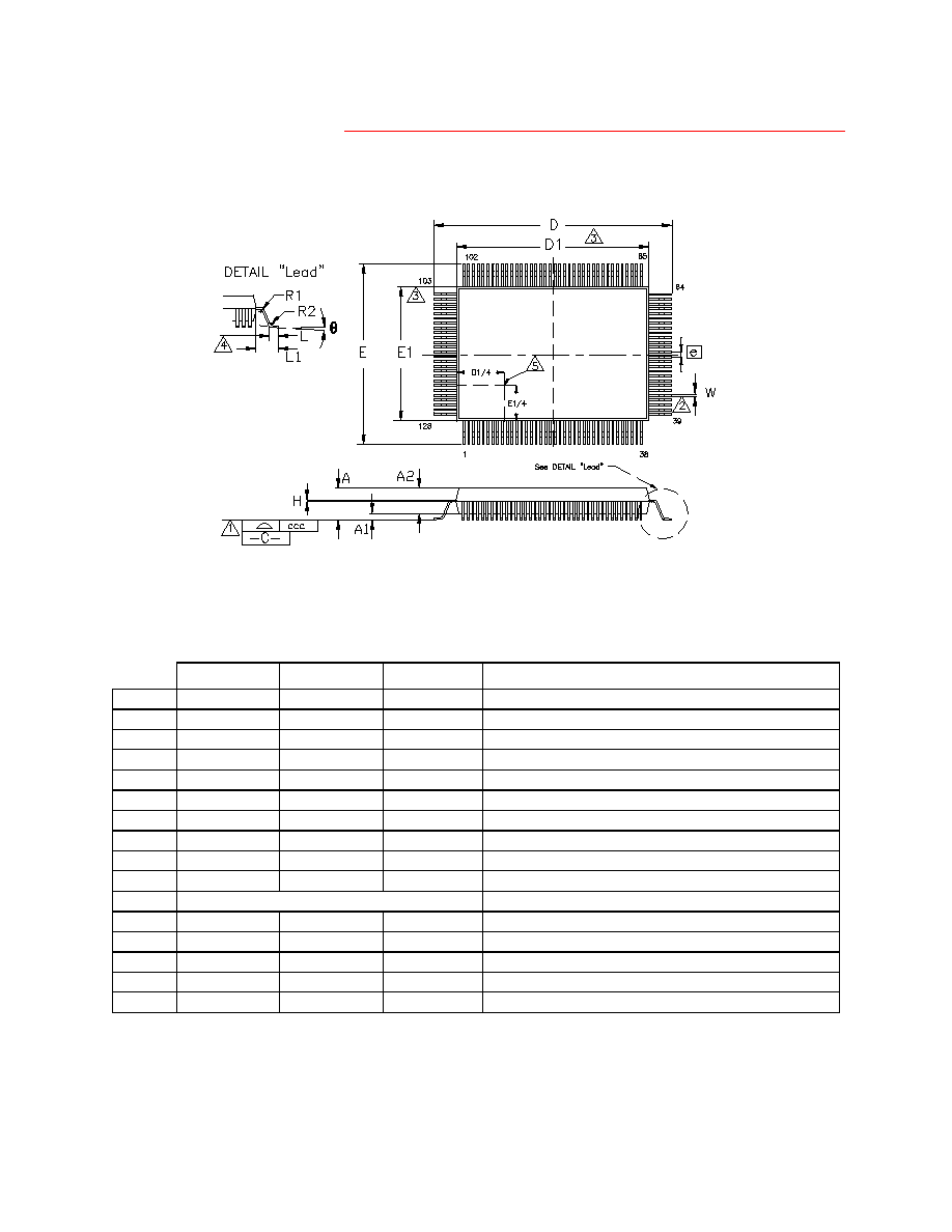
Package Outline
Figure 2 128 Pin QFP Package Outline, 14X20X2.7 Body, 3.2mm Footprint
Notes:
1. Controlling Unit: millimeter.
2. Tolerance on the position of the leads is � 0.04 mm maximum.
3. Package body dimensions D1 and E1 do not include the mold protrusion.
Maximum mold protrusion is 0.25 mm.
4. Dimension for foot length L measured at the gauge plane 0.25 mm above the seating plane.
5. Details of pin 1 identifier are optional but must be located within the zone indicated.
Table 1 128 Pin QFP Package Parameters
MIN
NOMINAL
MAX
REMARKS
A
~
~
3.4
Overall Package Height
A1
0.05
~
0.5
Standoff
A2
2.55
~
3.05
Body Thickness
D
23.00
23.20
23.40
X Span
D1
19.90
20.00
20.10
X body Size
E
17.00
17.20
17.40
Y Span
E1
13.90
14.00
14.10
Y body Size
H
0.09
~
0.20
Lead Frame Thickness
L
0.73
0.88
1.03
Lead Foot Length
L1
~
1.60
~
Lead Length
e
0.50 Basic
Lead Pitch
q
0
o
~
7
o
Lead Foot Angle
W
0.10
~
0.30
Lead Width
R1
0.13
~
~
Lead Shoulder Radius
R2
0.13
~
0.30
Lead Foot Radius
ccc
~
~
0.08
Coplanarity