 | –≠–ª–µ–∫—Ç—Ä–æ–Ω–Ω—ã–π –∫–æ–º–ø–æ–Ω–µ–Ω—Ç: LPC47N207 | –°–∫–∞—á–∞—Ç—å:  PDF PDF  ZIP ZIP |
SMSC LPC47N207-JN
Page 1
Rev. 05-07-03
PRODUCT PREVIEW
LPC47N207
LPC Super I/O IrDA Hot Docking
Chip with UART
Data Brief
Product Features
3.3 Volt Operation (5V tolerant)
Programmable Wakeup Event Interface
(IO_PME# Pin)
SMI Support (IO_SMI# Pin)
GPIOs (16)
- Programmable internal pull-up resistors
Two IRQ Input Pins
XNOR Chain
PC99a and ACPI 1.0 Compliant
64 PIN STQFP Package
Intelligent Auto Power Management
One Full Function Serial Port
- High Speed 16C550A Compatible UARTs with
Send/Receive 16-Byte FIFOs
- Supports 230k and 460k Baud
- Programmable Baud Rate Generator
- Modem Control Circuitry
Infrared Communications Controller
- IrDA v1.2 (4Mbps), HPSIR, ASKIR, Consumer IR
Support
- 2 IR Ports
- 96 Base I/O Address, 15 IRQ Options and 3 DMA
Options
LPC Bus Host Interface
- Multiplexed Command, Address and Data Bus
- 8-Bit I/O Transfers
- 8-Bit DMA Transfers
- 16-Bit Address Qualification
- Serial IRQ Interface Compatible with Serialized IRQ
Support for PCI Systems
- PCI nCLKRUN Support
- Power Management Event (IO_PME#) Interface Pin
LPC PortSwitch
Interface
- Secondary Switchable LPC Interface (3.3V only)
- Buffered 14 MHz Output
- Switched PCI Clock output
ORDERING INFORMATION
Order Number(s):
LPC47N207-JN for 64 pin STQFP package

Rev. 05-07-03
Page 2
SMSC LPC47N207-JN
PRODUCT PREVIEW
© STANDARD MICROSYSTEMS CORPORATION (SMSC) 2003
80 Arkay Drive
Hauppauge, NY 11788
(631) 435-6000
FAX (631) 273-3123
Standard Microsystems and SMSC are registered trademarks of Standard Microsystems Corporation. Product names and company names are the
trademarks of their respective holders. Circuit diagrams utilizing SMSC products are included as a means of illustrating typical applications;
consequently complete information sufficient for construction purposes is not necessarily given. Although the information has been checked and is
believed to be accurate, no responsibility is assumed for inaccuracies. SMSC reserves the right to make changes to specifications and product
descriptions at any time without notice. Contact your local SMSC sales office to obtain the latest specifications before placing your product order. The
provision of this information does not convey to the purchaser of the semiconductor devices described any licenses under the patent rights of SMSC
or others. All sales are expressly conditional on your agreement to the terms and conditions of the most recently dated version of SMSC's standard
Terms of Sale Agreement dated before the date of your order (the "Terms of Sale Agreement"). The product may contain design defects or errors
known as anomalies which may cause the product's functions to deviate from published specifications. Anomaly sheets are available upon request.
SMSC products are not designed, intended, authorized or warranted for use in any life support or other application where product failure could cause
or contribute to personal injury or severe property damage. Any and all such uses without prior written approval of an Officer of SMSC and further
testing and/or modification will be fully at the risk of the customer. Copies of this document or other SMSC literature, as well as the Terms of Sale
Agreement, may be obtained by visiting SMSC's website at http://www.smsc.com.
SMSC DISCLAIMS AND EXCLUDES ANY AND ALL WARRANTIES, INCLUDING WITHOUT LIMITATION ANY AND ALL IMPLIED WARRANTIES
OF MERCHANTABILITY, FITNESS FOR A PARTICULAR PURPOSE, TITLE, AND AGAINST INFRINGEMENT AND THE LIKE, AND ANY AND
ALL WARRANTIES ARISING FROM ANY COURSE OF DEALING OR USAGE OF TRADE.
IN NO EVENT SHALL SMSC BE LIABLE FOR ANY DIRECT, INCIDENTAL, INDIRECT, SPECIAL, PUNITIVE, OR CONSEQUENTIAL DAMAGES,
OR FOR LOST DATA, PROFITS, SAVINGS OR REVENUES OF ANY KIND; REGARDLESS OF THE FORM OF ACTION, WHETHER BASED ON
CONTRACT, TORT, NEGLIGENCE OF SMSC OR OTHERS, STRICT LIABILITY, BREACH OF WARRANTY, OR OTHERWISE; WHETHER OR
NOT ANY REMEDY IS HELD TO HAVE FAILED OF ITS ESSENTIAL PURPOSE; AND WHETHER OR NOT SMSC HAS BEEN ADVISED OF THE
POSSIBILITY OF SUCH DAMAGES.

SMSC LPC47N207-JN
Page 3
Rev. 05-07-03
PRODUCT PREVIEW
General Description
The SMSC LPC47N207-JN is a 3.3V PC 99 and ACPI 1.0 compliant Super I/O Controller. The
LPC47N207-JN implements the LPC interface with the
LPC PortSwitch
Interface. T
he
LPC
PortSwitch
Interface is a hot-switchable external Docking LPC interface.
The LPC47N207-JN
also features a full 16-bit internally decoded address bus, a Serial IRQ interface with PCI nCLKRUN
support, relocatable configuration ports and three DMA channel options. The part also includes 16 GPIO
pins.
The LPC47N207-JN incorporates an eight pin 16C550A compatible UART. In addition, the LPC47N207-
JN provides a second UART to support a Serial Infrared Interface that complies with IrDA v1.2 (Fast IR),
HPSIR, and ASKIR formats (used by Sharp and other PDAs), as well as Consumer IR.
The LPC47N207-JN incorporates sophisticated power control circuitry (PCC). The PCC supports multiple
low power down modes. The LPC47N207-JN also features Software Configurable Logic (SCL) for ease of
use. SCL allows programmable system configuration of key functions such as the UARTs.
The LPC47N207-JN supports the ISA Plug-and-Play Standard register set (Version 1.0a) and provides the
recommended functionality to support Windows `9x, 2K, ME, XP and PC99. The I/O Address, DMA
Channel and Hardware IRQ of each device in the LPC47N207-JN may be reprogrammed through the
internal configuration registers. There are 192 I/O address location options, a Serialized IRQ interface,
and three DMA channels.
Rev. 05-07-03
Page 4
SMSC LPC47N207-JN
PRODUCT PREVIEW
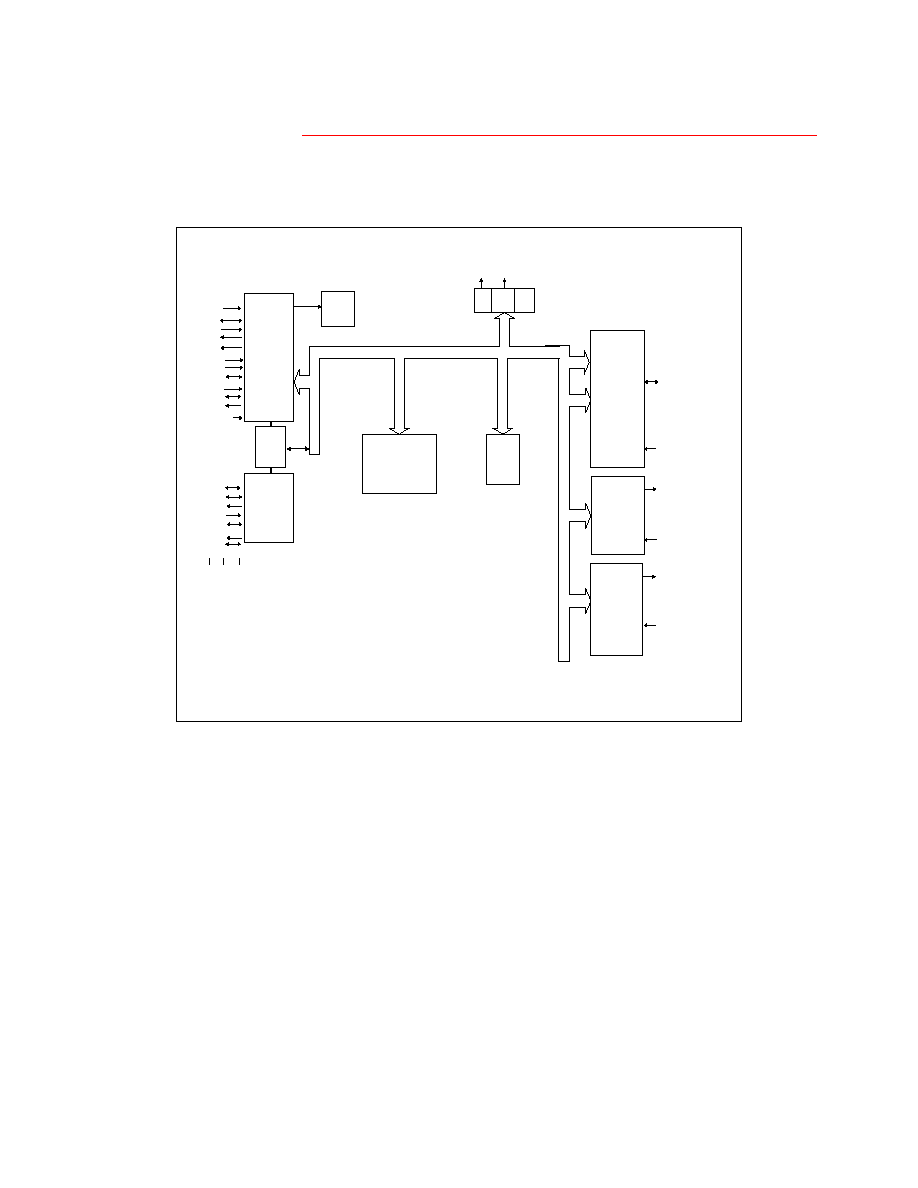
Block Diagram
TXD1, nRTS1, nDTR1
Vcc Vss
nIO_PME
IRTX2, IRMODE*
IRRX2, IRRX3*,
HOST
LPC BUS
INTERFACE
V
TR
CLOCK
GEN
SMI PME WDT
(UART1)
16C550
COMPATIBLE
SERIAL
PORT 1
nCTS1, RXD1,
nDSR1, nDCD1, nRI1
CONFIGURATION
REGISTERS
GENERAL
PURPOSE
I/O
GP30-GP37
GP10-GP11
GP15-GP17
GP12*, GP13*,
GP14*,
CONTROL, ADDRESS, DATA
ACPI
BLOCK
nIO_SMI*
16C550
COMPATIBLE
2 PIN
INFRARED
INTERFACE
SERIAL
PORT
IRQIN1*, IRQIN2*,
SIO_14M
LAD[3:0]
LFRAME#
LDRQ0#
LDRQ1#
PCI_RESET#
LPCPD#
nCLKRUN
PCI_CLK
SER_IRQ
nIO_PME
LPC_CLK_33
DSIO_14M
DLAD[3:0]
DLFRAME#
DLDRQ1#
nDCLKRUN
DLPC_CLK_33
DSER_IRQ
DOCK
LPC BUS
INTERFACE
DOCKING
LPC
SWITCHES
BUFFERS
AND
CONTROL
SIO_14M
Denotes Multifunction Pins
*
Figure 1 - LPC47N207-JN Block Diagram
SMSC LPC47N207-JN
Page 5
Rev. 05-07-03
PRODUCT PREVIEW
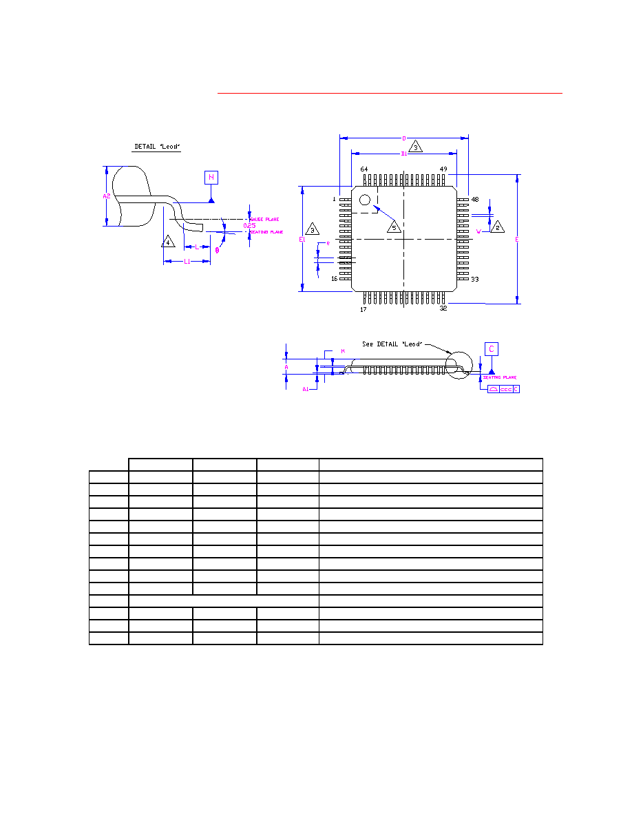
Package Outline
Figure 2 ≠ 64-Pin STQFP Package Outline
Table 1 - 64-Pin STQFP Package Parameters
MIN
NOMINAL
MAX
REMARKS
A
~ ~
1.60
Overall
Package Height
A1
0.05 ~ 0.15
Standoff
A2
1.35 1.40 1.45
Body Thickness
D
8.80 9.00 9.20
X
Span
D1
6.80 7.00 7.20
X
body Size
E
8.80 9.00 9.20
Y
Span
E1
6.80 7.00 7.20
Y
body Size
H
0.09
~
0.20
Lead Frame Thickness
L
0.45
0.60
0.75
Lead Foot Length
L1
~
1.00 REF.
~
Lead Length
e
0.40 Basic
Lead Pitch
0
o
~ 7
o
Lead Foot Angle
W
0.13 0.18 0.23
Lead
Width
ccc
~ ~
0.08
Coplanarity
Notes:
1. Controlling Unit: millimeter.
2. Tolerance on the true position of the leads is ± 0.035 mm maximum.
3. Package body dimensions D1 and E1 do not include the mold protrusion.
Maximum mold protrusion is 0.25 mm per side. D1 and E1 dimensions determined at datum plane H.
4. Dimension for foot length L measured at the gauge plane 0.25 mm above the seating plane.
5. Details of pin 1 identifier are optional but must be located within the zone indicated.