 | –≠–ª–µ–∫—Ç—Ä–æ–Ω–Ω—ã–π –∫–æ–º–ø–æ–Ω–µ–Ω—Ç: LPC47S422 | –°–∫–∞—á–∞—Ç—å:  PDF PDF  ZIP ZIP |

LPC47S42x
Enhanced Super I/O with LPC Interface for
Server Applications
FEATURES
∑
3.3 Volt Operation (5V Tolerant)
∑
Floppy Disk Controller (Supports Two FDCs)
∑
Multi-Mode Parallel Port
∑
Two UARTs
∑
8042 Keyboard Controller
∑
SMBus Controller
∑
X-Bus Interface
∑
Programmable Wakeup Event Interface
(nIO_PME Pin)
∑
SMI Support (nIO_SMI Pin)
∑
GPIOs (39)
∑
Fan Speed Control Output
∑
Fan Tachometer Input
∑
ISA IRQ to Serial IRQ Conversion
∑
XNOR Chain
∑
PC99 and ACPI 1.0 Compliant
∑
ISA Plug-and-Play Compatible Register Set
∑
Intelligent Auto Power Management
∑
2.88MB Super I/O Floppy Disk Controller
-
Licensed CMOS 765B Floppy Disk
Controller
-
Software and Register Compatible with
SMSC's Proprietary 82077AA
Compatible Core
-
Configurable Open Drain/Push-Pull
Output Drivers
-
Supports Vertical Recording Format
-
16-Byte Data FIFO
-
100% IBM
Æ
Compatibility
-
Detects All Overrun and Underrun
Conditions
-
Sophisticated Power Control Circuitry
(PCC) Including Multiple Powerdown
Modes for Reduced Power
Consumption
-
DMA Enable Logic
-
Data Rate and Drive Control Registers
-
480 Address, up to 15 IRQ and Three
DMA Options
∑
Enhanced Digital Data Separator
-
2 Mbps, 1 Mbps, 500 Kbps, 300 Kbps,
250 Kbps Data Rates
-
Programmable Precompensation
Modes
∑
Keyboard Controller
-
8042 Software Compatible
-
8-Bit Microcomputer
-
2k Bytes of Program ROM
-
256 Bytes of Data RAM
-
Four Open Drain Outputs Dedicated for
Keyboard/Mouse Interface
-
Asynchronous Access to Two Data
Registers and One Status Register
-
Supports Interrupt and Polling Access
-
8-Bit Counter Timer
-
Port 92 Support
-
Fast Gate A20 and KRESET Outputs
∑
Serial Ports
-
Two Full Function Serial Ports
-
High Speed NS16C550 Compatible
UARTs with Send/Receive 16-Byte
FIFOs
-
Supports 230k and 460k Baud
-
Programmable Baud Rate Generator
-
Modem Control Circuitry
-
480 Address and 15 IRQ Options
-
IrDA 1.0, HP-SIR, ASK IR Support

2
∑
Multi-Mode Parallel Port with ChiProtectTM
-
Standard Mode IBM PC/XT
Æ
, PC/AT
Æ
,
and PS/2TM Compatible Bidirectional
Parallel Port
-
Enhanced Parallel Port (EPP)
Compatible - EPP 1.7 and EPP 1.9
(IEEE 1284 Compliant)
-
IEEE 1284 Compliant Enhanced
Capabilities Port (ECP)
-
ChiProtect Circuitry for Protection
Against Damage Due to Printer Power-
On
-
480 Address, up to 15 IRQ and 3 DMA
Options
-
Multiplexed Command, Address and
Data Bus
-
8-Bit I/O Transfers
-
8-Bit DMA Transfers
-
16-Bit Address Qualification
-
Serial IRQ Interface Compatible with
Serialized IRQ Support for PCI Systems
-
Power Management Event (PME)
Interface Pin
∑
100 Pin QFP Package
GENERAL DESCRIPTION
The LPC47S42x* is a 3.3V PC99 compliant
Super I/O controller. The LPC47S42x
implements the LPC interface, a pin reduced ISA
interface which provides the same or better
performance as the ISA/X-bus with a substantial
savings in pins used. The part provides 39 GPIO
pins, an SMBus controller, a fan speed control
output, a fan tachometer input, four ISA IRQs
that can be routed to any of the serial IRQs, and
an X-Bus interface.
The LPC47S42x incorporates a keyboard
interface, SMSC's true CMOS 765B floppy disk
controller, advanced digital data separator, two
16C550 compatible UARTs, one Multi-Mode
parallel port which includes ChiProtect circuitry
plus EPP and ECP, and Intelligent Power
Management. The true CMOS 765B core
provides 100% compatibility with IBM PC/XT and
PC/AT architectures in addition to providing data
overflow and underflow protection. The SMSC
advanced digital data separator incorporates
SMSC's patented data separator technology,
allowing for ease of testing and use. The on-chip
UARTs are compatible with the NS16C550. The
parallel port is compatible with IBM PC/AT
architecture, as well as IEEE 1284 EPP and
ECP. The LPC47S42x incorporates
sophisticated power control circuitry (PCC). The
PCC supports multiple low power down modes.
The LPC47S42x supports the ISA Plug-and-Play
Standard (Version 1.0a) and provides the
recommended functionality to support Windows
'95/'98 and PC99. The I/O Address, DMA
Channel and Hardware IRQ of each logical
device in the LPC47S42x may be reprogrammed
through the internal configuration registers.
There are 480 I/O address location options, a
Serialized IRQ interface, and three DMA
channels.
Standard Microsystems is a registered trademark and
SMSC is a trademark of Standard Microsystems
Corporation. Other product and company names are
trademarks or registered trademarks of their respective
holders.
*The "x" in the part number is a designator that changes depending upon the particular BIOS used
inside the specific chip. "2" denotes AMI Keyboard BIOS and "7" denotes Phoenix 42i Keyboard BIOS.

3
TABLE OF CONTENTS
FEATURES ....................................................................................................................................... 1
GENERAL DESCRIPTION ................................................................................................................ 2
PIN CONFIGURATION ...................................................................................................................... 5
DESCRIPTION OF PIN FUNCTIONS ................................................................................................. 6
Buffer Type Descriptions............................................................................................................... 11
Pins That Require External Pullup Resistors.................................................................................. 12
3.3 VOLT OPERATION / 5 VOLT TOLERANCE .............................................................................. 13
POWER FUNCTIONALITY .............................................................................................................. 13
VCC Power .................................................................................................................................. 13
VTR Support ................................................................................................................................ 13
Internal PWRGOOD ..................................................................................................................... 13
32.768 kHz Trickle Clock Input...................................................................................................... 13
Indication of 32kHz Clock ............................................................................................................. 14
Trickle Power Functionality ........................................................................................................... 14
Maximum Current Values.............................................................................................................. 16
Power Management Events (PME/SCI)......................................................................................... 16
FUNCTIONAL DESCRIPTION ......................................................................................................... 17
Super I/O Registers ...................................................................................................................... 17
Host Processor Interface (LPC)..................................................................................................... 17
FLOPPY DISK CONTROLLER ........................................................................................................ 22
FDC Internal Registers ................................................................................................................. 22
Command Set/Descriptions .......................................................................................................... 40
Instruction Set .............................................................................................................................. 44
SERIAL PORT (UART).................................................................................................................... 72
INFRARED INTERFACE ................................................................................................................. 88
PARALLEL PORT........................................................................................................................... 89
POWER MANAGEMENT................................................................................................................112
SERIAL IRQ...................................................................................................................................116
Routable IRQ to Serial IRQ Conversion Capability........................................................................120
8042 KEYBOARD CONTROLLER DESCRIPTION .........................................................................121
Keyboard Interface ......................................................................................................................121
External Keyboard and Mouse Interface .......................................................................................123
Keyboard Power Management .....................................................................................................123
Interrupts.....................................................................................................................................124
Memory Configurations................................................................................................................124
Register Definitions .....................................................................................................................124
External Clock Signal...................................................................................................................125
Default Reset Conditions .............................................................................................................125
Latches On Keyboard and Mouse IRQs .......................................................................................128
Keyboard and Mouse PME Generation ........................................................................................130
GENERAL PURPOSE I/O...............................................................................................................131
GPIO Pins...................................................................................................................................131
Description..................................................................................................................................132
GPIO Control ..............................................................................................................................135
GPIO Operation ..........................................................................................................................136
GPIO PME and SMI Functionality ................................................................................................137
Either Edge Triggered Interrupts ..................................................................................................139
LED Functionality ........................................................................................................................139

4
WATCH DOG TIMER .....................................................................................................................140
SYSTEM MANAGEMENT INTERRUPT (SMI) .................................................................................140
SMI Registers..............................................................................................................................141
ACPI Support Register for SMI Generation...................................................................................142
PME Support .................................................................................................................................142
Wake On Specific Key Option ......................................................................................................143
FAN SPEED CONTROL AND MONITORING..................................................................................145
Fan Speed Control ......................................................................................................................145
Fan Tachometer Input .................................................................................................................146
SECURITY FEATURE ....................................................................................................................150
GPIO Device Disable Register Control .........................................................................................150
Device Disable Register...............................................................................................................150
SMBus CONTROLLER ..................................................................................................................150
Overview.....................................................................................................................................150
Configuration Registers ...............................................................................................................151
Runtime Registers .......................................................................................................................151
Pin Multiplexing ...........................................................................................................................158
SMBus Timeouts .........................................................................................................................158
X-BUS INTERFACE .......................................................................................................................160
X-Bus Chip Select Base I/O Address Registers ............................................................................163
X-Bus Configuration Register.......................................................................................................163
RUNTIME REGISTERS ..................................................................................................................164
Runtime Registers Block Summary ..............................................................................................164
Runtime Registers Block Description............................................................................................168
CONFIGURATION..........................................................................................................................200
OPERATIONAL DESCRIPTION .....................................................................................................229
Maximum Guaranteed Ratings.....................................................................................................229
DC Electrical Characteristics........................................................................................................229
TIMING DIAGRAMS .......................................................................................................................233
ECP Parallel Port Timing .............................................................................................................244
X-Bus Timing ..............................................................................................................................253
PACKAGE OUTLINE .....................................................................................................................261
APPENDIX - TEST MODES............................................................................................................262
Board Test Mode.........................................................................................................................262
80 Arkay Drive
Hauppauge, NY 11788
(516) 435-6000
FAX (516) 273-3123
5
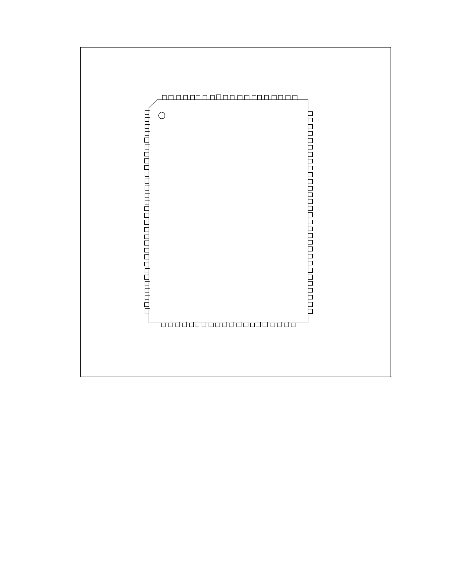
PIN CONFIGURATION
LPC47S42x
100 PIN QFP
GP40/DRVDEN0
GP41/DRVDEN1/nXCS0
nMTR0
nDSKCHG
nDS0
CLKI32
VSS
nDIR
nSTEP
nWDATA
nWGATE
nHDSEL
nINDEX
nTRK0
nWRTPRT
nRDATA
GP42/nIO_PME
VTR
CLOCKI
LAD0
LAD1
LAD2
LAD3
nLFRAME
nLDRQ
nPCI_RESET
nLPCPD
GP43/DDRC/nXCS1
PCI_CLK
SER_IRQ
1
2
3
4
5
6
7
8
9
10
11
12
13
14
15
16
17
18
19
20
21
22
23
24
25
26
27
28
29
30
nACK
BUSY
PE
SLCT
VSS
PD7
PD6
PD5
PD4
PD3
PD2
PD1
PD0
nSLCTIN
nINIT
VCC
GP37/nA20M
GP36/nKBDRST
GP35/IRQINB
GP34/IRQINA
VSS
MCLK
MDAT
KCLK
KDAT
GP33/FAN/XA1
GP32/SDAT/XA0
VCC
GP31/FAN_TACH/nXCS3/XA3
GP30/SCLK/nXCS2/XA2
80
79
78
77
76
75
74
73
72
71
70
69
68
67
66
65
64
63
62
61
60
59
58
57
56
55
54
53
52
51
V
S
S
G
P
1
0
/
X
D
0
G
P
1
1
/
X
D
1
G
P
1
2
/
X
D
2
G
P
1
3
/
X
D
3
G
P
1
4
/
X
D
4
G
P
1
5
/
X
D
5
G
P
1
6
/
X
D
6
G
P
1
7
/
X
D
7
G
P
6
2
/
P
1
7
/
I
R
Q
I
N
C
G
P
2
0
/
P
1
7
/
n
D
S
1
G
P
2
1
/
P
1
6
/
P
1
2
G
P
2
2
/
P
1
2
/
n
M
T
R
1
G
P
2
3
/
I
R
Q
I
N
D
G
P
2
4
/
S
Y
S
O
P
T
G
P
2
5
/
n
X
R
D
G
P
2
6
/
n
X
W
R
G
P
6
0
/
L
E
D
1
G
P
6
1
/
L
E
D
2
G
P
2
7
/
n
I
O
_
S
M
I
3
1
3
2
3
3
3
4
3
5
3
6
3
7
3
8
3
9
4
0
4
1
4
2
4
3
4
4
4
5
4
6
4
7
4
8
4
9
5
0
G
P
5
7
/
n
D
T
R
2
G
P
5
6
/
n
C
T
S
2
G
P
5
5
/
n
R
T
S
2
G
P
5
4
/
n
D
S
R
2
G
P
5
3
/
T
X
D
2
/
I
R
T
X
G
P
5
2
/
R
X
D
2
/
I
R
R
X
G
P
5
1
/
n
D
C
D
2
V
C
C
G
P
5
0
/
n
R
I
2
n
D
C
D
1
n
R
I
1
n
D
T
R
1
n
C
T
S
1
n
R
T
S
1
n
D
S
R
1
T
X
D
1
R
X
D
1
n
S
T
R
O
B
E
n
A
L
F
n
E
R
R
O
R
1
0
0
9
9
9
8
9
7
9
6
9
5
9
4
9
3
9
2
9
1
9
0
8
9
8
8
8
7
8
6
8
5
8
4
8
3
8
2
8
1