
SMSC USB3300
PRODUCT PREVIEW
Revision 1.02 (02-16-05)
Data Brief
PRODUCT FEATURES
USB3300
Hi-Speed USB Host or
Device PHY with ULPI
Low Pin Interface
USB-IF "Hi-Speed" certified to the Universal Serial
Bus Specification Rev 2.0
Interface compliant with the ULPI Specification
revision 1.1 in 8-bit mode.
Industry standard UTMI+ Low Pin Interface (ULPI.)
Converts 54 UTMI+ signals into a standard 12 pin
Link controller interface.
Supports FS pre-amble for FS hubs with a LS device
attached (UTMI+ Level 3)
Supports HS SOF and LS keep-alive pulse.
Includes full support for the optional On-The-Go
(OTG) protocol detailed in the On-The-Go
Supplement Revision 1.0a specification.
Supports the OTG Host Negotiation Protocol (HNP)
and Session Request Protocol (SRP.)
Allows host to turn VBUS off to conserve battery
power in OTG applications.
Supports OTG monitoring of VBUS levels with
internal comparators. Includes support for an external
VBUS or fault monitor.
Low Latency Hi-Speed Receiver (43 Hi-Speed clocks
Max) allows use of legacy UTMI Links with a ULPI
wrapper.
Integrated Pull-up resistor on STP for interface
protection allows a reliable Link/PHY start-up with
slow Links (software configured for low power.)
Internal 1.8 volt regulators allow operation from a
single 3.3 volt supply.
Internal short circuit protection of ID, DP and DM
lines to VBUS or ground.
Integrated 24MHz Crystal Oscillator supports either
crystal operation or 24MHz external clock input.
Internal PLL for 480MHz Hi-Speed USB operation.
54.7mA Unconfigured Current (typical) - ideal for bus
powered applications.
83uA suspend current (typical) - ideal for battery
powered applications.
Full Commercial operating temperature range from
0C to +70C.
32 pin QFN package; green, lead-free (5 x 5 x 0.90
mm height)
ORDER NUMBER(S): USB3300-EZK FOR 32 PIN, QFN PACKAGE (GREEN, LEAD-FREE)
80 Arkay Drive
Hauppauge, NY 11788
(631)
435-6000
FAX (631) 273-3123
Copyright � SMSC 2005. All rights reserved.
Circuit diagrams and other information relating to SMSC products are included as a means of illustrating typical applications. Consequently, complete
information sufficient for construction purposes is not necessarily given. Although the information has been checked and is believed to be accurate, no
responsibility is assumed for inaccuracies. SMSC reserves the right to make changes to specifications and product descriptions at any time without
notice. Contact your local SMSC sales office to obtain the latest specifications before placing your product order. The provision of this information does
not convey to the purchaser of the described semiconductor devices any licenses under any patent rights or other intellectual property rights of SMSC
or others. All sales are expressly conditional on your agreement to the terms and conditions of the most recently dated version of SMSC's standard
Terms of Sale Agreement dated before the date of your order (the "Terms of Sale Agreement"). The product may contain design defects or errors
known as anomalies which may cause the product's functions to deviate from published specifications. Anomaly sheets are available upon request.
SMSC products are not designed, intended, authorized or warranted for use in any life support or other application where product failure could cause
or contribute to personal injury or severe property damage. Any and all such uses without prior written approval of an Officer of SMSC and further
testing and/or modification will be fully at the risk of the customer. Copies of this document or other SMSC literature, as well as the Terms of Sale
Agreement, may be obtained by visiting SMSC's website at http://www.smsc.com. SMSC is a registered trademark of Standard Microsystems
Corporation ("SMSC"). Product names and company names are the trademarks of their respective holders.
SMSC DISCLAIMS AND EXCLUDES ANY AND ALL WARRANTIES, INCLUDING WITHOUT LIMITATION ANY AND ALL IMPLIED WARRANTIES
OF MERCHANTABILITY, FITNESS FOR A PARTICULAR PURPOSE, TITLE, AND AGAINST INFRINGEMENT AND THE LIKE, AND ANY AND
ALL WARRANTIES ARISING FROM ANY COURSE OF DEALING OR USAGE OF TRADE.
IN NO EVENT SHALL SMSC BE LIABLE FOR ANY DIRECT, INCIDENTAL, INDIRECT, SPECIAL, PUNITIVE, OR CONSEQUENTIAL DAMAGES;
OR FOR LOST DATA, PROFITS, SAVINGS OR REVENUES OF ANY KIND; REGARDLESS OF THE FORM OF ACTION, WHETHER BASED ON
CONTRACT; TORT; NEGLIGENCE OF SMSC OR OTHERS; STRICT LIABILITY; BREACH OF WARRANTY; OR OTHERWISE; WHETHER OR
NOT ANY REMEDY OF BUYER IS HELD TO HAVE FAILED OF ITS ESSENTIAL PURPOSE, AND WHETHER OR NOT SMSC HAS BEEN
ADVISED OF THE POSSIBILITY OF SUCH DAMAGES.
Hi-Speed USB Host or Device PHY with ULPI Low Pin Interface
Revision 1.02 (02-16-05)
2
SMSC USB3300
PRODUCT PREVIEW

Hi-Speed USB Host or Device PHY with ULPI Low Pin Interface
SMSC USB3300
3
Revision 1.02 (02-16-05)
PRODUCT PREVIEW
General Description
The USB3300 is a stand-alone Hi-Speed USB Physical Layer Transceiver (PHY). The USB3300 uses
a low pin count interface (ULPI) to connect to a ULPI compliant Link layer. The ULPI interface reduces
the UTMI+ interface from 54 pins to 12 pins using a method of in-band signaling and status byte
transfers between the Link and PHY.
This PHY was designed from the start with the ULPI interface. No UTMI to ULPI wrappers are used
in this design which provides a seamless ULPI to Link interface. The result is a PHY with a low latency
transmit and receive time. SMSC's low latency high speed and full speed receiver provide the option
of re-using existing UTMI Links with a simple wrapper to convert UTMI to ULPI.
The ULPI interface allows the USB3300 PHY to operate as a device, host, or an On-The-Go (OTG)
device. Designs using the USB3300 PHY as a device, can add host and OTG capability at a later date
with no additional pins.
The ULPI interface, combined with SMSC's proprietary technology, makes the USB3300 the ideal
method of adding Hi-Speed USB to new designs. The USB3300 features an industry leading small
footprint package (5mm by 5mm) with sub 1mm height. In addition the USB3300 integrates all DP and
DM termination resistances and requires a minimal number of external components.
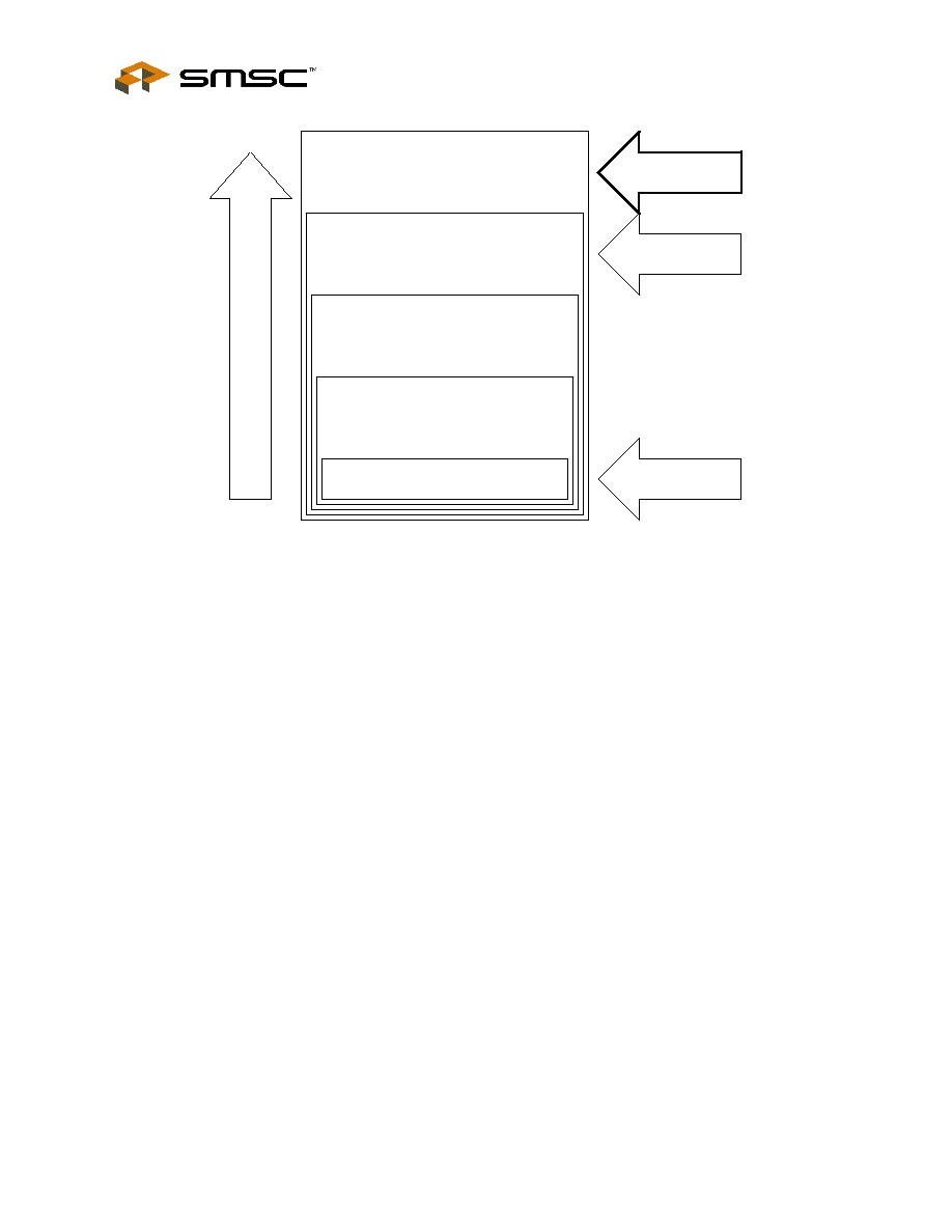
Figure 1 Basic ULPI USB Device Block Diagram
The ULPI interface consists of 12 interface pins; 8 bi-directional data pins, 3 control pins, and a 60
MHz clock. By using the 12 pin ULPI interface the USB3300 is able to provide support for the full range
of UTMI+ Level 3 through Level 0, as shown in Figure 2, "ULPI Interface Features as Related to
UTMI+". This allows USB3300 to work as a HS and FS peripheral and as a HS, FS, and LS Host.
The USB3300 can also, as an option, fully support the On-the-Go (OTG) protocol defined in the On-
The-Go Supplement to the USB 2.0 Specification. On-the-Go allows the USB3300 to function like a
host, or peripheral configured dynamically by software. For example, a cell phone may connect to a
computer as a peripheral to exchange address information or connect to a printer as a host to print
pictures. Finally the OTG enabled device can connect to another OTG enabled device to exchange
information. All this is supported using a single low profile Mini-AB USB connector.
Designs not needing OTG can ignore the OTG feature set.
In addition to the advantages of the leading edge ULPI interface, the use of SMSC's advanced analog
technology enables the USB3300 to consume a minimum amount of power which results in maximized
battery life for portable applications.
USB3300
USB 2.0
Analog
w/ OTG
ULPI
Digital
Logic
USB
Connector
(Standard
or Mini)
ULPI
LINK
DM
V
BUS
DP
ID
STP
CLK
DIR
NXT
DATA[7:0]
32 Pin QFN
Hi-Speed USB Host or Device PHY with ULPI Low Pin Interface
Revision 1.02 (02-16-05)
4
SMSC USB3300
PRODUCT PREVIEW
Figure 2 ULPI Interface Features as Related to UTMI+
Applications
The USB3300 is targeted for any application where a Hi-Speed USB connection is desired and when
board space and interface pins must be minimized.
The USB3300 is well suited for:
Cell Phones
MP3 Players
Scanners
External Hard Drives
Still and Video Cameras
Portable Media Players
Entertainment Devices
UTMI+ Level 0
USB2.0 Peripherals Only
AD
DED
FEA
T
UR
ES
USB3300
ULPI
USB2.0 Peripheral, host controllers, On-the-
Go devices with 12 pin interface
(HS, FS, LS, preamble packet)
UTMI+ Level 3
USB2.0 Peripheral, host controllers, On-the-
Go devices
(HS, FS, LS, preamble packet)
UTMI+ Level 2
USB2.0 Peripheral, host controllers, On-
the-Go devices
(HS, FS, and LS but no preamble packet)
UTMI+ Level 1
USB2.0 Peripheral, host controllers, and
On-the-Go devices
(HS and FS Only)
USB3500
USB3450
USB3280
USB3250

Hi-Speed USB Host or Device PHY with ULPI Low Pin Interface
SMSC USB3300
5
Revision 1.02 (02-16-05)
PRODUCT PREVIEW
Block Diagram
The USB3300 is a highly integrated USB PHY. It contains a complete Hi-Speed USB2.0 PHY with the
ULPI industry standard interface to support fast time to market for a USB product. The USB3300 is
composed of the functional blocks shown in Figure 3, "USB3300 Block Diagram" below.
Figure 3 USB3300 Block Diagram
ULPI Digital
OTG
Module
DATA[7:0]
24 MHz
XTAL
Internal
Regulator &
POR
5V
Power
Supply
Bias
Gen.
CLKOUT
NXT
DIR
STP
VDD3.3
XTAL &
PLL
XI
CPEN
VBUS
ID
VDD3.3
DP
DM
USB3300
VD
D
1
.
8
VDDA1
.
8
m
XO
RBIAS
EXTVBUS
FAULT
Mini-AB
USB
Connector
HS XCVR
FS/LS
XCVR
Resistors
Rpu_d
p
R
p
d
_dm
R
p
d
_dp
Rpu_d
m
EN