
iv
TABLE OF CONTENTS
1
GENERAL DESCRIPTION.................................................................................................................... 1
2
FEATURES............................................................................................................................................ 2
3
ORDERING INFORMATION ................................................................................................................. 2
4
BLOCK DIAGRAM ................................................................................................................................ 3
5
DIE PAD ARRANGEMENT................................................................................................................... 4
6
PIN DESCRIPTION ............................................................................................................................... 8
7
FUNCTIONAL BLOCK DESCRIPTIONS............................................................................................ 10
8
COMMAND TABLE............................................................................................................................. 17
9
COMMAND DESCRIPTIONS.............................................................................................................. 25
10
MAXIMUM RATINGS....................................................................................................................... 35
11
DC CHARACTERISTICS................................................................................................................. 35
12
AC CHARACTERISTICS................................................................................................................. 38
13
APPLICATION EXAMPLES ............................................................................................................ 41
14
APPENDIX ....................................................................................................................................... 42

SOLOMON SYSTECH
SEMICONDUCTOR TECHNICAL DATA
This document contains information on a new product under definition stage. Solomon Systech Limited reserves
the right to change or discontinue this product without notice.
http://www.solomon-systech.com
SSD0852
Rev 1.0
P 1/44
Feb 2003
Copyright
2003 Solomon Systech Limited
SSD0852
Advance Information
LCD Segment / Common Driver
With Controller
CMOS
1 General
Description
SSD0852 is a single-chip CMOS LCD driver with controller for liquid crystal dot-matrix graphic
display system. It consists of 257 high voltage driving output pins for driving 128 Segments, 128
Commons and an ICON line.
SSD0852 displays data directly from its internal 128x129x2 bits Graphic Display Data RAM
(GDDRAM). Data/Commands are sent through I
2
C interface.
SSD0852 embeds a DC-DC Converter, an LCD Voltage Regulator, an On-Chip Bias Divider and an
On-Chip Oscillator, which reduce the number of external components. With the special design on
minimizing power consumption and die/package layout, SSD0852 is suitable for any portable battery-
driven applications requiring a long operation period and compact size.

Solomon Systech
Feb 2003
P 2/44
Rev 1.0
SSD0852
2 FEATURES
128 x 128 Dot-matrix 4-gray levels Display Driver with an Icon Line
Single Supply Operation, 1.8 V � 3.3 V
Minimum +8.0V LCD Driving Output Voltage
Maximum +15 V LCD Driving Output Voltage
Low Current Sleep Mode
On-Chip Voltage Generator or External LCD Driving Power Supply Selectable
On-chip Oscillator with external resistor
On-chip Bias Divider
On-chip 128x129x2bits Graphic Display Data RAM
3X/4X/5X/6X DC � DC Converter
Programmable Multiplex ratio in dot-matrix display area from 16Mux ~ 129Mux
Programmable bias ratio from 1/5 ~ 1/12
I
2
C interface
Re-mapping of Row & Column Drivers
Vertical Scrolling
Display Offset Control
64 Level Internal Contrast Control
External Contrast Control
Programmable LCD Driving Voltage Temperature Coefficients from TC0 (-0.05%/
o
C) to TC7 (-
0.25%/
o
C)
Programmable COM Output Sequence
Direct Memory Access Mode
Selectable Internal/External Oscillator Resistor
Available in Gold Bump Die and TAB (Tape Automated Bonding) Package
3 ORDERING
INFORMATION
Table 1 - Ordering Information
Ordering Part
Number
Seg
Com
Default Bias
Package Form
SSD0852Z
128
128 + 1
1/12
Gold Bump Die
SSD0852TR1 128
128
1/12
TAB
SSD0852
Rev 1.0
P 3/44
Feb 2003
Solomon Systech
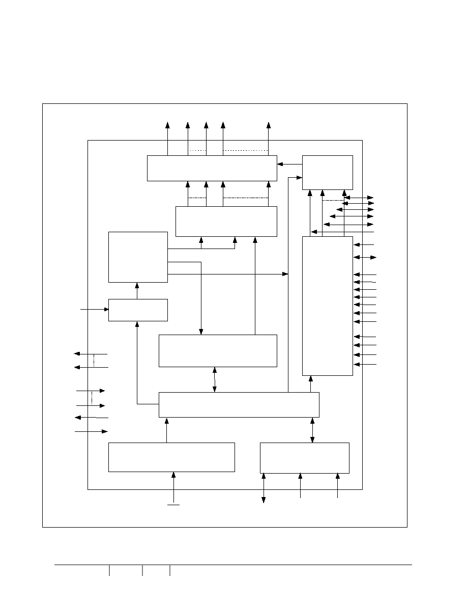
4 BLOCK
DIAGRAM
Figure 1 - Block Diagram
ROW0 ~
ROW127
ICONS
SEG0 ~ SEG 127
HV Buffer Cell Level Shifter
Level Selector
Display Data Latch
Display
Timing
Generator
Oscillator
GDDRAM
128 X 129 X 2 Bits
Command Decoder
Command Interface
I
2
C Interface
LCD Driving
Voltage
Generator
3X / 4X / 5X /
6X DC/DC
Converter,
Voltage
Regulator,
Bias Divider,
Contrast
Control,
Temperature
Compensation
V
L6
V
L5
V
L4
V
L3
V
L2
V
SS
V
R
V
CC
C
3P
C
4P
C
5P
C
2N
C
1P
C
2P
REF
INTRS
V
CI
V
EXT
SDA SCL SA0
RES
V
DD
V
SS
OSC1
C
1N
TEST0
:
TEST17
TEST_IN0
:
TEST_IN6
Solomon Systech
Feb 2003
P 4/44
Rev 1.0
SSD0852
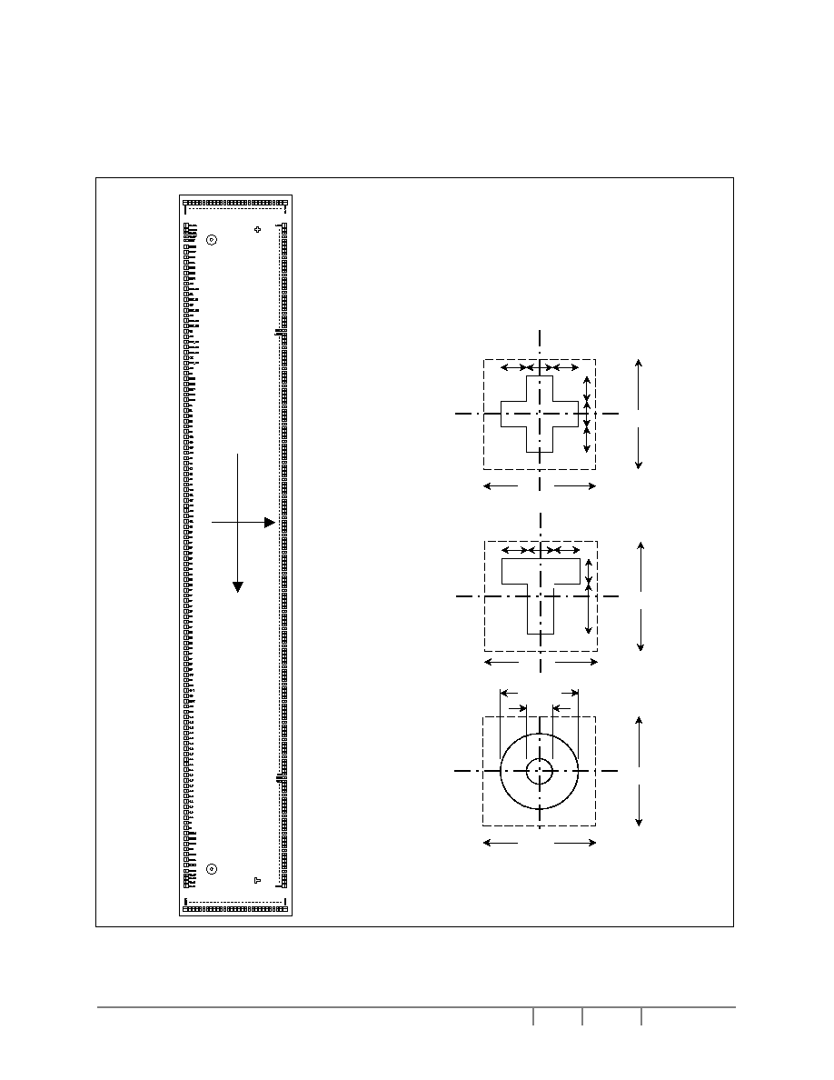
5 DIE PAD ARRANGEMENT
Figure 2 - Die Pad Assignment
Die Size: 10.49 mm x 1.72 mm
Die Thickness: 533�25�m
Bump Height: Typical 18�m
Bump co-planarity <3�m (within die)
25
25
25
25
25
25
100
100
25
25
25
25
50
100
100
18
100
75
100
Note:
1. Diagram showing the face of the
die.
2. Coordinates are reference to
center of the chip.
3. Unit of coordinates and Size of all
alignment marks are in
�m.
4. All alignment keys do not contain
gold bump.
x
y
(
0,0
)
Cent
er :
-4518,
-342
Cent
er :
-4706,
320
Cent
er :
4518,
-342
Cent
er 4683,
320
Pin 1 ->
SSD0852
Rev 1.0
P 5/44
Feb 2003
Solomon Systech
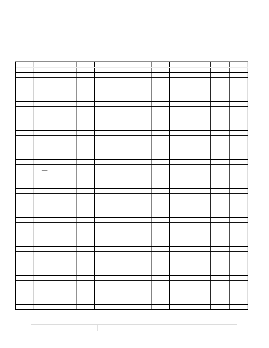
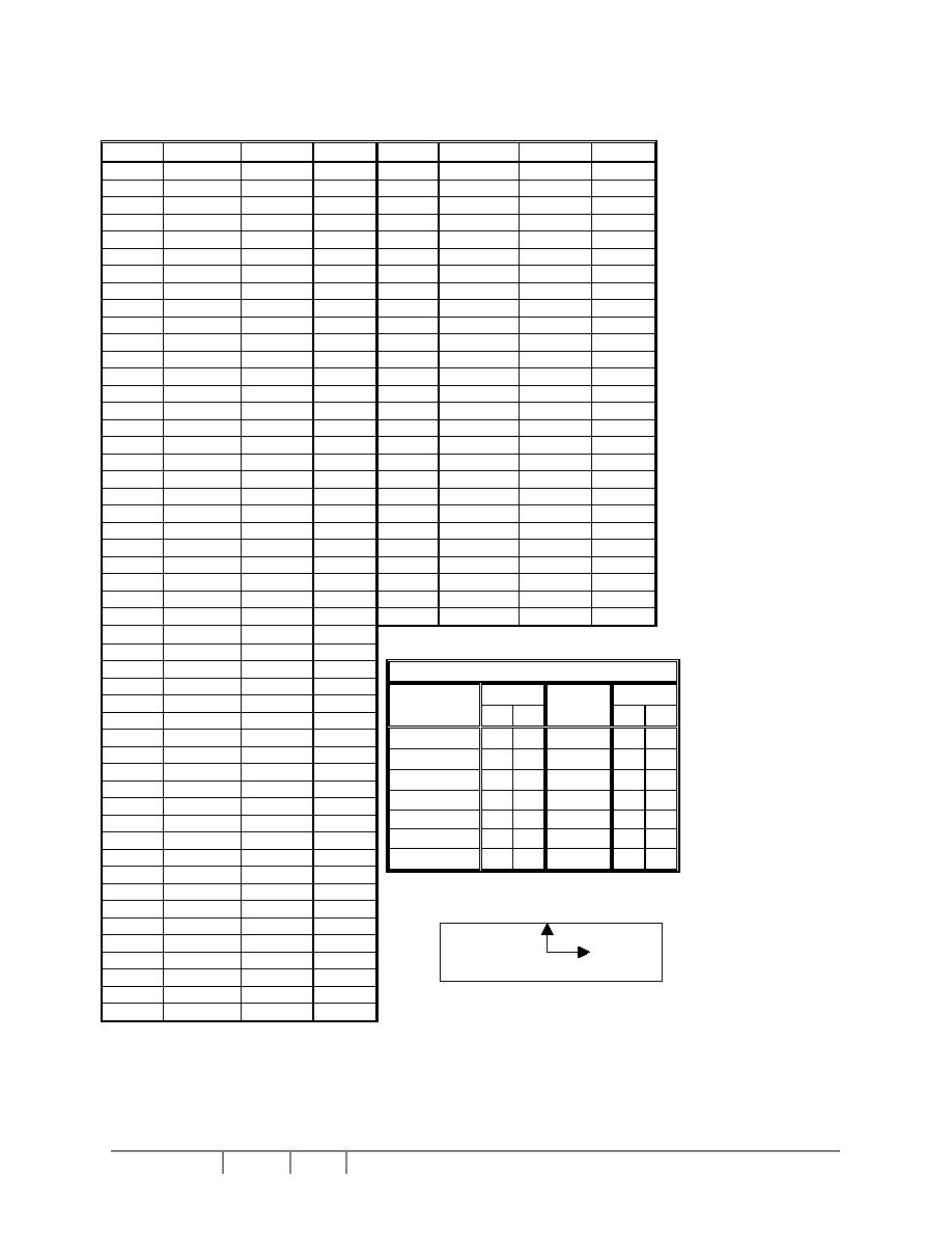
Table 2 - SSD0852 Bump Die Pad Coordinates
Pad # Signal
X-pos
Y-pos
Pad # Signal
X-pos
Y-pos
Pad # Signal
X-pos
Y-pos
1 ROW124
-4763.1
-705.0 51 V
CI
-1028.9
-702.8 101 V
L3
2781.1
-702.8
2 ROW125
-4700.1
-705.0 52 V
SS
-952.7
-702.8 102 V
L3
2857.3
-702.8
3 ROW126
-4650.1
-705.0 53 V
SS
-876.5
-702.8 103 V
L4
2933.5
-702.8
4 ROW127
-4600.1
-705.0 54 V
SS
-800.3
-702.8 104 V
L4
3009.7
-702.8
5 ICONS
-4550.1
-705.0
55 V
SS
-724.1
-702.8 105 V
L4
3085.9
-702.8
6 TEST13
-4457.9
-702.8 56 V
CC
-647.9
-702.8 106 V
L4
3162.1
-702.8
7 TEST17
-4381.7
-702.8 57 V
CC
-571.7
-702.8 107 V
L5
3238.3
-702.8
8 TEST0
-4305.5
-702.8
58 V
CC
-495.5
-702.8 108 V
L5
3314.5
-702.8
9 TEST1
-4229.3
-702.8
59 V
CC
-419.3
-702.8 109 V
L5
3390.7
-702.8
10 TEST2
-4153.1
-702.8 60 C
5P
-343.1
-702.8 110 V
L5
3466.9
-702.8
11 TEST3
-4076.9
-702.8 61 C
5P
-266.9
-702.8 111 V
L6
3543.1
-702.8
12 TEST4
-4000.7
-702.8 62 C
5P
-190.7
-702.8 112 V
L6
3619.3
-702.8
13 VDD
-3924.5
-702.8
63 C
3P
-114.5
-702.8 113 V
L6
3695.5
-702.8
14
TEST_IN0
-3848.3 -702.8 64
C
3P
-38.3
-702.8
114 V
L6
3771.7
-702.8
15 V
SS
-3772.1
-702.8 65 C
3P
37.9
-702.8
115 V
R
3847.9
-702.8
16
TEST_IN1
-3695.9 -702.8 66
C
3P
114.1
-702.8
116 V
R
3924.1
-702.8
17 V
DD
-3619.7
-702.8 67 C
1N
190.3
-702.8
117 TEST14
4000.3
-702.8
18
TEST_IN2
-3543.5 -702.8 68
C
1N
266.5
-702.8
118 TEST15
4076.5
-702.8
19 V
SS
-3467.3
-702.8 69 C
1N
342.7
-702.8
119 TEST16
4152.7
-702.8
20
TEST_IN3
-3391.1 -702.8 70
C
1N
418.9
-702.8
120 OSC1 4228.9
-702.8
21
TEST_IN3
-3314.9 -702.8 71
C
1P
495.1
-702.8
121 TEST10
4305.1
-702.8
22
RES
-3238.7 -702.8 72
C
1P
571.3
-702.8
122 TEST11
4381.3
-702.8
23 V
DD
-3162.5
-702.8 73 C
1P
647.5
-702.8
123 TEST13
4457.5
-702.8
24
TEST_IN4
-3086.3 -702.8 74
C
1P
723.7
-702.8
124 TEST12
4544.9
-705.0
25
TEST_IN4
-3010.1 -702.8 75
C
2P
799.9
-702.8
125 ROW63
4599.9
-705.0
26
TEST_IN5
-2933.9 -702.8 76
C
2P
876.1
-702.8
126 ROW62
4649.9
-705.0
27 V
SS
-2857.7
-702.8 77 C
2P
952.3
-702.8
127 ROW61
4699.9
-705.0
28
TEST_IN6
-2781.5 -702.8 78
C
2P
1028.5
-702.8 128 ROW60
4762.9
-705.0
29 V
DD
-2705.3
-702.8 79 C
2N
1104.7
-702.8 129 ROW59
5094.1
-713.0
30 SD0
-2629.1
-702.8
80 C
2N
1180.9
-702.8 130 ROW58
5094.1
-650.0
31 TEST5
-2552.9
-702.8 81 C
2N
1257.1
-702.8 131 ROW57
5094.1
-600.0
32 TEST6
-2476.7
-702.8 82 C
2N
1333.3
-702.8 132 ROW56
5094.1
-550.0
33 TEST7
-2400.5
-702.8 83 C
4P
1409.5
-702.8 133 ROW55
5094.1
-500.0
34 TEST8
-2324.3
-702.8 84 C
4P
1485.7
-702.8 134 ROW54
5094.1
-450.0
35 TEST9
-2248.1
-702.8 85 C
4P
1561.9
-702.8 135 ROW53
5094.1
-400.0
36 SCL
-2171.9
-702.8
86 C
4P
1638.1
-702.8 136 ROW52
5094.1
-350.0
37 SCL
-2095.7
-702.8
87 V
DD
1714.3
-702.8 137 ROW51 5094.1
-300.0
38
SDA -2019.5 -702.8 88
REF 1790.5 -702.8 138 ROW50 5094.1 -250.0
39 SDA
-1943.3
-702.8
89 V
SS
1866.7
-702.8 139 ROW49
5094.1
-200.0
40 SDA
-1867.1
-702.8
90 V
EXT
1942.9 -702.8 140 ROW48 5094.1
-150.0
41 SDA
-1790.9
-702.8
91 V
DD
2019.1
-702.8 141 ROW47 5094.1
-100.0
42 V
DD
-1714.7
-702.8 92 INTRS
2095.3
-702.8 142 ROW46 5094.1 -50.0
43 V
DD
-1638.5
-702.8 93 V
SS
2171.5
-702.8 143 ROW45
5094.1 0.0
44 V
DD
-1562.3
-702.8 94 V
SS
2247.7
-702.8 144 ROW44
5094.1 50.0
45 V
DD
-1486.1
-702.8 95 V
L2
2323.9 -702.8 145 ROW43 5094.1 100.0
46 V
CI
-1409.9
-702.8 96 V
L2
2400.1 -702.8 146 ROW42 5094.1 150.0
47 V
CI
-1333.7
-702.8 97 V
L2
2476.3 -702.8 147 ROW41 5094.1 200.0
48 V
CI
-1257.5
-702.8 98 V
L2
2552.5 -702.8 148 ROW40 5094.1 250.0
49 V
CI
-1181.3
-702.8 99 V
L3
2628.7 -702.8 149 ROW39 5094.1 300.0
50 V
CI
-1105.1
-702.8
100 V
L3
2704.9 -702.8 150 ROW38 5094.1 350.0

Solomon Systech
Feb 2003
P 6/44
Rev 1.0
SSD0852
Pad # Signal
X-pos
Y-pos
Pad # Signal
X-pos
Y-pos
Pad # Signal
X-pos
Y-pos
151 ROW37
5094.1
400.0 201 SEG11 2599.9 705.0 251 SEG61 99.9 705.0
152 ROW36
5094.1
450.0 202 SEG12 2549.9 705.0 252 SEG62 49.9 705.0
153 ROW35
5094.1
500.0 203 SEG13 2499.9 705.0 253 SEG63 -0.1 705.0
154 ROW34
5094.1
550.0 204 SEG14 2449.9 705.0 254 SEG64 -50.1 705.0
155 ROW33
5094.1
600.0 205 SEG15 2399.9 705.0 255 SEG65 -100.1 705.0
156 ROW32
5094.1
650.0 206 SEG16 2349.9 705.0 256 SEG66 -150.1 705.0
157 ROW31
5094.1
713.0 207 SEG17 2299.9 705.0 257 SEG67 -200.1 705.0
158 ROW30
4762.9
705.0 208 SEG18 2249.9 705.0 258 SEG68 -250.1 705.0
159 ROW29
4699.9
705.0 209 SEG19 2199.9 705.0 259 SEG69 -300.1 705.0
160 ROW28
4649.9
705.0 210 SEG20 2149.9 705.0 260 SEG70 -350.1 705.0
161 ROW27
4599.9
705.0 211 SEG21 2099.9 705.0 261 SEG71 -400.1 705.0
162 ROW26
4549.9
705.0 212 SEG22 2049.9 705.0 262 SEG72 -450.1 705.0
163 ROW25
4499.9
705.0 213 SEG23 1999.9 705.0 263 SEG73 -500.1 705.0
164 ROW24
4449.9
705.0 214 SEG24 1949.9 705.0 264 SEG74 -550.1 705.0
165 ROW23
4399.9
705.0 215 SEG25 1899.9 705.0 265 SEG75 -600.1 705.0
166 ROW22
4349.9
705.0 216 SEG26 1849.9 705.0 266 SEG76 -650.1 705.0
167 ROW21
4299.9
705.0 217 SEG27 1799.9 705.0 267 SEG77 -700.1 705.0
168 ROW20
4249.9
705.0 218 SEG28 1749.9 705.0 268 SEG78 -750.1 705.0
169 ROW19
4199.9
705.0 219 SEG29 1699.9 705.0 269 SEG79 -800.1 705.0
170 ROW18
4149.9
705.0 220 SEG30 1649.9 705.0 270 SEG80 -850.1 705.0
171 ROW17
4099.9
705.0 221 SEG31 1599.9 705.0 271 SEG81 -900.1 705.0
172 ROW16
4049.9
705.0 222 SEG32 1549.9 705.0 272 SEG82 -950.1 705.0
173 ROW15
3999.9
705.0 223 SEG33 1499.9 705.0 273 SEG83 -1000.1 705.0
174 ROW14
3949.9
705.0 224 SEG34 1449.9 705.0 274 SEG84 -1050.1 705.0
175 ROW13
3899.9
705.0 225 SEG35 1399.9 705.0 275 SEG85 -1100.1 705.0
176 ROW12
3849.9
705.0 226 SEG36 1349.9 705.0 276 SEG86 -1150.1 705.0
177 ROW11
3799.9
705.0 227 SEG37 1299.9 705.0 277 SEG87 -1200.1 705.0
178 ROW10
3749.9
705.0 228 SEG38 1249.9 705.0 278 SEG88 -1250.1 705.0
179 ROW9 3699.9
705.0 229 SEG39 1199.9 705.0 279 SEG89 -1300.1 705.0
180 ROW8 3649.9
705.0 230 SEG40 1149.9 705.0 280 SEG90 -1350.1 705.0
181 ROW7 3599.9
705.0 231 SEG41 1099.9 705.0 281 SEG91 -1400.1 705.0
182 ROW6 3549.9
705.0 232 SEG42 1049.9 705.0 282 SEG92 -1450.1 705.0
183 ROW5 3499.9
705.0 233 SEG43 999.9 705.0 283 SEG93 -1500.1 705.0
184 ROW4 3449.9
705.0 234 SEG44 949.9 705.0 284 SEG94 -1550.1 705.0
185 ROW3 3399.9
705.0 235 SEG45 899.9 705.0 285 SEG95 -1600.1 705.0
186 ROW2 3349.9
705.0 236 SEG46 849.9 705.0 286 SEG96 -1650.1 705.0
187 ROW1 3299.9
705.0 237 SEG47 799.9 705.0 287 SEG97 -1700.1 705.0
188 ROW0 3249.9
705.0 238 SEG48 749.9 705.0 288 SEG98 -1750.1 705.0
189 ICONS 3199.9
705.0 239 SEG49 699.9 705.0 289 SEG99 -1800.1 705.0
190 SEG0 3149.9 705.0 240 SEG50 649.9 705.0 290 SEG100
-1850.1 705.0
191 SEG1 3099.9 705.0 241 SEG51 599.9 705.0 291 SEG101
-1900.1 705.0
192 SEG2 3049.9 705.0 242 SEG52 549.9 705.0 292 SEG102
-1950.1 705.0
193 SEG3 2999.9 705.0 243 SEG53 499.9 705.0 293 SEG103
-2000.1 705.0
194 SEG4 2949.9 705.0 244 SEG54 449.9 705.0 294 SEG104
-2050.1 705.0
195 SEG5 2899.9 705.0 245 SEG55 399.9 705.0 295 SEG105
-2100.1 705.0
196 SEG6 2849.9 705.0 246 SEG56 349.9 705.0 296 SEG106
-2150.1 705.0
197 SEG7 2799.9 705.0 247 SEG57 299.9 705.0 297 SEG107
-2200.1 705.0
198 SEG8 2749.9 705.0 248 SEG58 249.9 705.0 298 SEG108
-2250.1 705.0
199 SEG9 2699.9 705.0 249 SEG59 199.9 705.0 299 SEG109
-2300.1 705.0
200 SEG10 2649.9
705.0 250 SEG60 149.9 705.0 300 SEG110
-2350.1
705.0
SSD0852
Rev 1.0
P 7/44
Feb 2003
Solomon Systech
Pad # Signal
X-pos
Y-pos
Pad # Signal
X-pos
Y-pos
301 SEG111 -2400.1 705.0 351 ROW97 -5094.3 600.0
302 SEG112 -2450.1 705.0 352 ROW98 -5094.3 550.0
303 SEG113 -2500.1 705.0 353 ROW99 -5094.3 500.0
304 SEG114 -2550.1 705.0 354 ROW100
-5094.3 450.0
305 SEG115 -2600.1 705.0 355 ROW101
-5094.3 400.0
306 SEG116 -2650.1 705.0 356 ROW102
-5094.3 350.0
307 SEG117 -2700.1 705.0 357 ROW103
-5094.3 300.0
308 SEG118 -2750.1 705.0 358 ROW104
-5094.3 250.0
309 SEG119 -2800.1 705.0 359 ROW105
-5094.3 200.0
310 SEG120 -2850.1 705.0 360 ROW106
-5094.3 150.0
311 SEG121 -2900.1 705.0 361 ROW107
-5094.3 100.0
312 SEG122 -2950.1 705.0 362 ROW108
-5094.3 50.0
313 SEG123 -3000.1 705.0 363 ROW109
-5094.3 0.0
314 SEG124 -3050.1 705.0 364 ROW110
-5094.3 -50.0
315 SEG125 -3100.1 705.0 365 ROW111
-5094.3 -100.0
316 SEG126 -3150.1 705.0 366 ROW112
-5094.3 -150.0
317 SEG127 -3200.1 705.0 367 ROW113
-5094.3 -200.0
318 ROW64 -3250.1 705.0 368 ROW114
-5094.3
-250.0
319 ROW65 -3300.1 705.0 369 ROW115
-5094.3
-300.0
320 ROW66 -3350.1 705.0 370 ROW116
-5094.3
-350.0
321 ROW67 -3400.1 705.0 371 ROW117
-5094.3
-400.0
322 ROW68 -3450.1 705.0 372 ROW118
-5094.3
-450.0
323 ROW69 -3500.1 705.0 373 ROW119
-5094.3
-500.0
324 ROW70 -3550.1 705.0 374 ROW120
-5094.3
-550.0
325 ROW71 -3600.1 705.0 375 ROW121
-5094.3
-600.0
326 ROW72 -3650.1 705.0 376 ROW122
-5094.3
-650.0
327 ROW73 -3700.1 705.0 377 ROW123
-5094.3
-713.0
328 ROW74 -3750.1 705.0
329 ROW75 -3800.1 705.0
330 ROW76 -3850.1 705.0
331 ROW77 -3900.1 705.0
332 ROW78 -3950.1 705.0
333 ROW79 -4000.1 705.0
334 ROW80 -4050.1 705.0
335 ROW81 -4100.1 705.0
336 ROW82 -4150.1 705.0
337 ROW83 -4200.1 705.0
338 ROW84 -4250.1 705.0
339 ROW85 -4300.1 705.0
340 ROW86 -4350.1 705.0
341 ROW87 -4400.1 705.0
342 ROW88 -4450.1 705.0
343 ROW89 -4500.1 705.0
344 ROW90 -4550.1 705.0
345 ROW91 -4600.1 705.0
346 ROW92 -4650.1 705.0
347 ROW93 -4700.1 705.0
348 ROW94 -4763.1 705.0
349 ROW95 -5094.3 713.0
350 ROW96 -5094.3 650.0
Bump size :
Size Size
Pad
X Y
Pad
X Y
1 59 65
157
65
59
2~5 33 65
158
59
65
6~123 50 60 159~347 33
65
124~127 33 65
348 59
65
128 59 65
349
65
59
129 65 59 350~376 65
33
130~156 65 33
377 65
59
Remarks: TEST0~17 and TEST_IN0~6 are used for internal test. TEST0~17 should be left open.
TEST_IN0 should be connected to V
DD
and TEST_IN1~6 should be connected to V
SS
.
1
x
die
face
128
129
348
377
349
157
158
y

Solomon Systech
Feb 2003
P 8/44
Rev 1.0
SSD0852
6 PIN
DESCRIPTION
6.1 RES
This pin is reset signal input. When the pin is low, initialization of the chip is executed.
6.2 SDA, SCL & SA0
These pins are bi-directional data bus to be connected to the MCU in I
2
C-bus interface. Please
refer to the section: IIC Communication interface on page 10 for detail pin descriptions.
6.3 INTRS
This pin is an input pin to enable the internal resistors network for the voltage regulator when
INTRS is high. When external regulator is used, this pin must be connected to V
SS
, and external
resistors R
2
/R
1
should be connected to V
L6
, V
R
and V
SS
.
6.4 REF
This pin is an input pin to enable the internal reference voltage used for the internal regulator.
When it is high, an internal reference voltage source will be used. When it is low, an external
reference voltage source must be provided in V
EXT
pin if internal regulator is used.
6.5 V
DD
Power supply pin.
6.6 V
SS
Ground.
6.7 V
CI
Reference voltage input for internal DC-DC converter. The voltage of generated V
CC
equals to the
multiple factor (3X, 4X, 5X or 6X) times V
CI
with respect to V
SS
.
Note: voltage at this input pin must be larger than or equal to V
DD.
6.8 V
CC
This is the most positive voltage supply pin of the chip. It can be supplied externally or generated
by the internal DC-DC converter.
When using internal DC-DC converter as generator, voltage at this pin is for internal reference
only. It CANNOT be used for driving external circuitry.
6.9 C
1P
,C
2P
,C
3P
,C
4P
,C
5P
,C
1N
and C
2N
When internal DC-DC voltage converter is used, external capacitor(s) is/are connected among
these pins.
6.10 V
L6
This pin is the most positive LCD driving voltage. It can be supplied externally or generated by the
internal regulator.
6.11 V
R
This pin is an input of the internal voltage regulator. When the internal resistors network for the
voltage regulator is disabled (INTRS is pulled low), external resistors should be connected between
V
SS
and V
R
, and V
R
and V
L6
, respectively.
SSD0852
Rev 1.0
P 9/44
Feb 2003
Solomon Systech
6.12 V
EXT
This pin is an input to provide an external voltage reference for the internal voltage regulator when
REF pin is pulled L.
6.13 V
L5
, V
L4
, V
L3
, and V
L2
LCD driving voltages. They can be supplied externally or generated by the internal bias divider.
They have the following relationship:
V
L6
> V
L5
> V
L4
> V
L3
> V
L2
> V
SS
1:a
bias
V
L5
(a-1)/a*V
L6
V
L4
(a-2)/a*V
L6
V
L3
2/a*V
L6
V
L2
1/a*V
L6
6.14 ROW0~ROW127
These pins provide the row driving signals COM0 � COM127 to the LCD panel.
6.15 ICONS
This pin is the special icons line ROW signal output.
6.16 SEG0~SEG127
These pins provide the LCD column driving signals. Their voltage level is V
SS
during sleep mode
and standby mode.
6.17 OSC1
This pin connect to on-chip oscillator when external resistor connected between OSC1 and V
DD
and send a start oscillator ON command, the on-chip oscillator will operation and its frequency is
controlled by external resistor.
6.18 TEST0~TEST17
These pins are used for internal test and should NOT be connected to any signal pins nor shorted
together. They should be left open.
6.19 TEST_IN0~TEST_IN6
These pins are used for internal test. TEST_IN0 should be connected to V
DD
and TEST_IN1~6
should be connected to V
SS
.
6.20 NC
The No Connection pin should NOT be connected to any signal pins nor shorted to other NC pins
in application. It should be left open.

Solomon Systech
Feb 2003
P 10/44 Rev 1.0
SSD0852
7 FUNCTIONAL BLOCK DESCRIPTIONS
7.1 I
2
C communication Interface
The IIC communication interface consists of slave address bit (SA0), I
2
C-bus data signal (SDA)
and I
2
C-bus clock signal (SCL). Both the SDA and the SCL must be connected to pull-up resistors.
There are also an input signal
RES
which is used for the initialization of device.
a) Slave address bit (SA0)
SSD0852 has to recognize the slave address before transmitting or receiving any information by
the I
2
C-bus. The device will responds to the slave address following by the slave address bit
("SA0" bit) and the read/write select bit ("R/W" bit) with the following byte format,
b
7
b
6
b
5
b
4
b
3
b
2
b
1
b
0
0 1 1 1 1 0 SA0 R/W
"SA0" bit provides an extension bit for the slave address. Either "0111100" or "0111101" can be
selected as the slave address of SSD0852.
"R/W" bit determines the I
2
C-bus interface is operating at either write mode or read status mode.
b) I
2
C-bus data signal (SDA)
SDA acts as a communication channel between the transmitter and the receiver. The data and
the acknowledgement are sent through the SDA.
It should be noticed that the ITO track resistance and the pulled-up resistance at "SDA" pin
becomes a voltage potential divider. As a result, the acknowledgement would not be possible to
attain a valid logic 0 level in "SDA".
c) I
2
C-bus clock signal (SCL)
The transmission of information in the I
2
C-bus is following a clock signal, SCL. Each transmission
of data bit is taken place during a single clock period of SCL.
7.2 Command
Decoder
Input is directed to the command decoder based on the input of control byte which consists of a
D/C bit and a R/W bit. For further information about the control byte, please refer to the section
"I
2
C-bus Write data and read register status" on page 22. If both the D/C bit and the R/W bit are
low, the input signal is interpreted as a Command. It will be decoded and written to the
corresponding command register. If the D/C bit is high and the R/W bit is low, input signal is written
to Graphic Display Data RAM (GDDRAM).
7.3 Oscillator
Circuit
This module is an On-Chip low power oscillator circuitry with external resistor. The oscillator
generates the clock for the DC-DC voltage converter. This clock is also used in the Display Timing
Generator block
Figure 3 - Oscillator Circuit
Oscillator
Circuit
OSC
V
DD
OSC1

SSD0852
Rev 1.0
P 11/44 Feb 2003
Solomon Systech
7.4 LCD Driving voltage Generator and Regulator
This module generates the LCD voltage needed for display output. It takes a single supply input
and generates necessary bias voltages. It consists of:
1. 3X, 4X, 5X and 6X DC-DC voltage converter
Please refer to Figure 4.
Figure 4 - DC-DC Converter Configurations
2. Voltage Regulator
The feedback gain control for LCD driving contrast curves can be selected by INTRS pin to either
internal (INTRS pin = H) or external (INTRS pin = L). If internal resistor network is enabled, eight
settings can be selected through software command. If external control is selected, external
resistors are required to be connected between V
SS
and V
R
(R
1
), and between V
R
and V
L6
(R
2
).
See application circuit diagrams for detail connections.
3. Contrast Control (Voltages referenced to V
SS
)
Software control of the 64-contrast voltage levels at each voltage regulator feedback gain. The
equation of calculating the LCD driving voltage is given as:
V
SS
V
CC
C
5P
C
3P
C
1N
C
1P
C
2P
C
2N
C
4P
+
-
-
+
-
+
3X Boost
V
SS
V
CC
C
5P
C
3P
C
1N
C
1P
C
2P
C
2N
C
4P
+
-
-
+
-
+
+
4X Boost
V
SS
V
CC
C
5P
C
3P
C
1N
C
1P
C
2P
C
2N
C
4P
+
-
-
+
-
+
+
+
5X Boost
+
-
V
SS
V
CC
C
5P
C
3P
C
1N
C
1P
C
2P
C
2N
C
4P
+
-
-
+
-
+
+
+
6X Boost
Remarks: capacitor = 1.0 ~ 4.7uF
out
L
V
R
R
V
*
1
1
2
6
+
=
ref
out
V
V
*
210
63
1
-
-
=
where
,
V
V
ref
4
.
1
=

Solomon Systech
Feb 2003
P 12/44 Rev 1.0
SSD0852
Figure 5 - Voltage Regulator Output for Different Gain/Contrast Settings (V
DD
= 2.775V; V
CI
= 3V;
DC-DC level = 6X; TC2 = -0.125%/
o
C)
4. Bias Divider
If the output op-amp buffer option in Set Power Control Register command is enabled, this circuit
block will divide the regulator output (V
L6
) to give the LCD driving levels (V
L2
- V
L5
).
A low power consumption circuit design in this bias divider saves most of the display current
comparing to traditional design.
5. Bias Ratio Selection circuitry
Software control of 1/5 to 1/12 bias ratio is used to match the characteristic of LCD panel.
6. Self adjust temperature compensation circuitry
Provide 8 different compensation grade selections to satisfy the various liquid crystal
temperature grades. The grading can be selected by software control. Default temperature
coefficient (TC) value is -0.125%/
o
C.
VL6 Vs Contrast
0
2
4
6
8
10
12
14
16
0
10
20
30
40
50
60
70
Contrast[0~63]
VL6[V]
IR0
IR1
IR2
IR3
IR4
IR5
IR6
IR7

SSD0852
Rev 1.0
P 13/44 Feb 2003
Solomon Systech
7.5 Graphic Display Data RAM (GDDRAM)
The GDDRAM is a bit mapped static RAM holding the bit pattern to be displayed. The size of the
RAM is 128 x 129 x 2 = 33024bits. Figure 6 is a description of the GDDRAM address map.
For mechanical flexibility, re-mapping on both Segment and Common outputs are provided.
For vertical scrolling of display, an internal register storing the display start line can be set to control
the portion of the RAM data mapped to the display. Figure 6 shows the case in which the display
start line register is set at 70H.
For those GDDRAM out of the display common range, they could still be accessed, for either
preparation of vertical scrolling data or even for the system usage.
7.6 Reset
Circuit
This block includes Power On Reset circuitry and the hardware reset pin,
RES
. Both of these have
the same reset function. Once
RES
receives a negative reset pulse, all internal circuitry will start to
initialize. Minimum pulse width for completing the reset sequence is 10us. Status of the chip after
reset is given by:
Register Default
Value
Descriptions
Page address
0
Column address
0
Display ON/OFF
0
Display OFF
Display Start Line
0
GDDRAM page 0,D0
Display Offset
0
COM0 is mapped to ROW0
Mux Ratio
80H
128 Mux
Normal/Reverse Display
0
Normal Display
N-line Inversion
0
No N-line Inversion
Entire Display
0
Entire Display is OFF
DC-DC booster
0
3X booster is selected
Internal Resistor Ratio
0
Gain = 3.45 (IR0)
Contrast 20H
LCD Bias Ratio
7
1/12 Bias Ratio
Scan direction of COM
0
Normal Scan direction
Segment Re-map
0
Segment re-map is disabled
Internal oscillator
0
Internal oscillator is OFF
Power save mode
0
Power save mode is OFF
Data display length
0
FRC, PWM Mode
0
4FRC, 9PWM
White Palette
(0, 0, 0, 0)
Light Gray Palette
(0, 0, 0, 0)
Dark Gray Palette
(9, 9, 9, 9)
Black Palette
(9, 9, 9, 9)
Temperature coefficient
2
PTC2 (-0.125%/
o
C)
Icon display
0
Icon display line is OFF
Power control
0,0,0
Booster, regulator & divider are both disabled
Scan sequence of COM
0
Normal Scan sequence
DMA mode
0
Disable DMA mode

Solomon Systech
Feb 2003
P 14/44 Rev 1.0
SSD0852
7.7 Display Data Latch
This block is a series of latches carrying the display signal information. These latches hold the
data, which will be fed to HV Buffer Cell and Level Selector to output the required voltage level.
The number of latches is 128+129= 257
7.8 HV Buffer Cell (Level Shifter)
HV Buffer Cell works as a level shifter which translates the low voltage output signal to the required
driving voltage. The output is shifted out with an internal FRM clock which comes from the Display
Timing Generator. The voltage levels are given by the level selector which is synchronized with the
internal M signal.
7.9 Level
Selector
Level Selector is a control of the display synchronization. Display voltage can be separated into
two sets and used with different cycles. Synchronization is important since it selects the required
LCD voltage level to the HV Buffer Cell, which in turn outputs the COM or SEG LCD waveform.
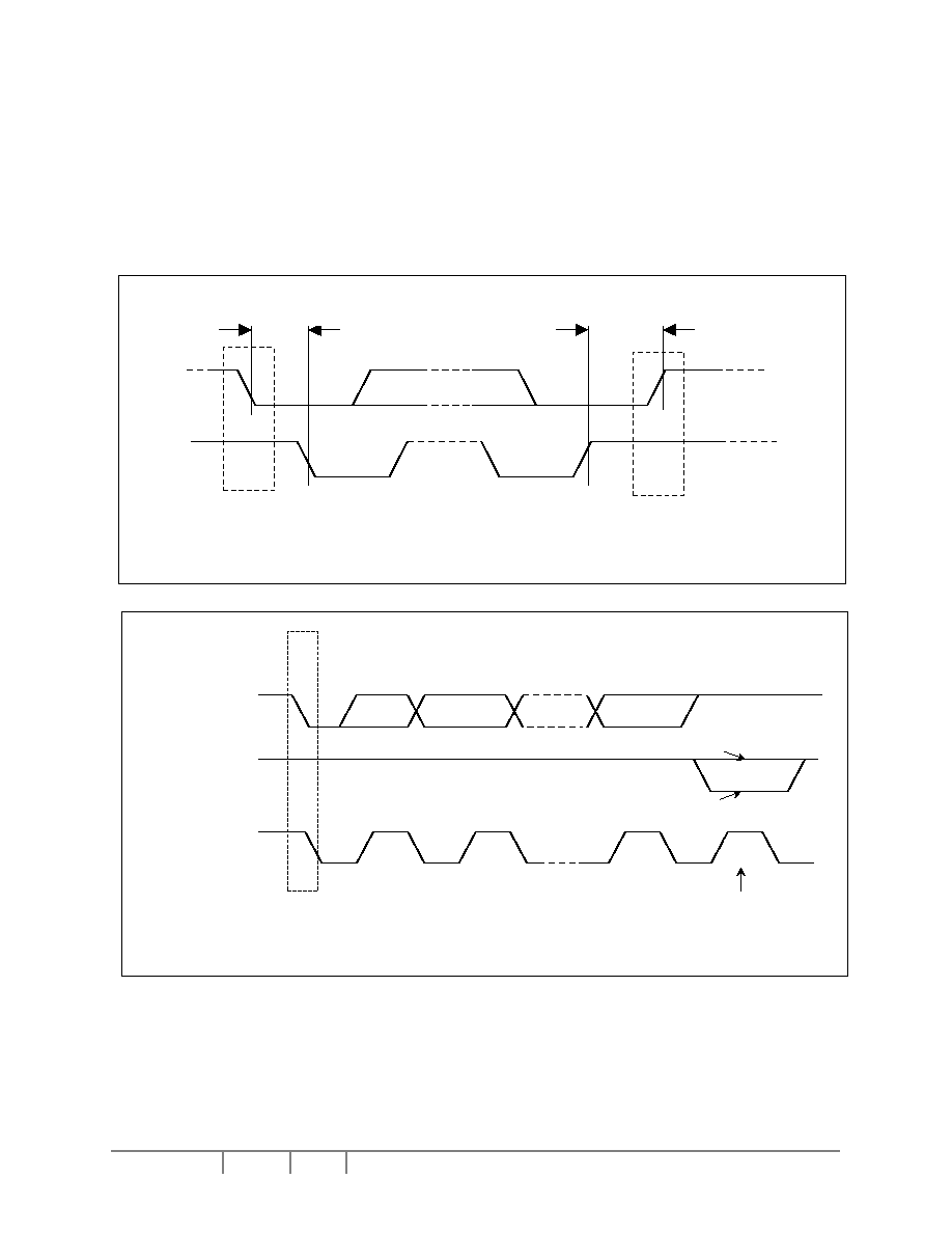
7.10 LCD Panel Driving Waveform
The following is an example of how the Common and Segment drivers may be connected to a LCD
panel. The waveforms are shown in Figure 7 illustrating the desired multiplex scheme with N-line
Inversion feature is disabled (default).
SSD0852
Rev 1.0
P 15/44 Feb 2003
Solomon Systech
Figure 6 - Graphic Display Data RAM (GDDRAM) Address Map with Display Start Line set to 70H
(MSB)
First Byte
(LSB)
Second Byte
Normal
Re-mapped
D3 D2 D2 D0
D 0
...........
0 0
COM16
COM111
D 1
...........
0 1
COM17
COM110
D 2
...........
0 2
COM18
COM109
D 3
...........
0 3
COM19
COM108
D 4
...........
0 4
COM20
COM107
D 5
...........
0 5
COM21
COM106
D 6
...........
0 6
COM22
COM105
D 7
...........
0 7
COM23
COM104
D 0
...........
0 8
COM24
COM103
D 1
...........
0 9
COM25
COM102
D 2
...........
0 A
COM26
COM101
D 3
...........
0 B
COM27
COM100
D 4
...........
0 C
COM28
COM99
D 5
...........
0 D
COM29
COM98
D 6
...........
0 E
COM30
COM97
D 7
...........
0 F
COM31
COM96
D 0
...........
3 0
COM0
COM127
D 1
...........
3 1
COM1
COM126
D 2
...........
3 2
COM2
COM125
D 3
...........
3 3
COM3
COM124
D 4
...........
3 4
COM4
COM123
D 5
...........
3 5
COM5
COM122
D 6
...........
3 6
COM6
COM121
D 7
...........
3 7
COM7
COM120
D 0
...........
3 8
COM8
COM119
D 1
...........
3 9
COM9
COM118
D 2
...........
3 A
COM10
COM117
D 3
...........
3 B
COM11
COM116
D 4
...........
3 C
COM12
COM115
D 5
...........
3 D
COM13
COM114
D 6
...........
3 E
COM14
COM113
D 7
...........
3 F
COM15
COM112
Page 16 * -
-
-
-
D 0
...........
4 0
ICONS
ICONS
(*) Page address is set to 16, if only ICON control register is set to '1' (A3Hex)
Internal Column Address
00
01
02
03
04
05
06
07 ...........
F8
F9
FA
FB
FC
FD
FE
FF
SEG Re-map = 0
...........
SEG Re-map = 1
...........
SEG Outputs
...........
...............
...............
...............
SEG
124
03
SEG
125
SEG
126
SEG
127
SEG
0
SEG
1
SEG
2
SEG
3
02
01
00
7F
7E
7D
7C
Page Address
Line
Address
00
01
02
03
7C
7D
7E
7F
Page 1
...............
Page 14
Page 15
1
1
1
1
1
1
1
0
...............
...............
...............
...............
Page 0
0
0
0
0
0
0
0
1
Remarks: Column address will be incremented automatically after writing MSB and LSB.
Solomon Systech
Feb 2003
P 16/44 Rev 1.0
SSD0852
1
2
3
4
5 6 7 8 9
. . .
N
*
TIME SLOT
COM0
COM1
V
L6
V
L
5
V
L
4
V
L
3
V
L
2
V
SS
1
2
3
4
5
6
7
8
9
. . .
N
*
SEG0
SEG1
V
L6
V
L
5
V
L
4
V
L
3
V
L
2
V
SS
V
L6
V
L
5
V
L
4
V
L
3
V
L
2
V
SS
V
L6
V
L
5
V
L
4
V
L
3
V
L
2
V
SS
1 2 3 4 5 6 7 8 9
. . .
N
* 1 2 3 4 5 6 7 8
9
. . .
N
*
COM1
COM2
COM3
COM4
COM5
COM6
COM7
S
E
G
1
S
E
G
2
S
E
G
3
S
E
G
4
COM0
S
E
G
0
Figure 7 - LCD Driving Waveform for Displaying "0" (0 line inversion)
* Note : N is the number of multiplex ratio including Icon line if it is enabled, N is equal to 128 on POR.
SSD0852
Rev 1.0
P 17/44 Feb 2003
Solomon Systech
8 COMMAND
TABLE
Table 3 - Command Table
Bit Pattern
Command
Description
0000 C
3
C
2
C
1
C
0
Set Lower Column
Address
Set the lower nibble of the column address pointer for
RAM access. The pointer is reset to 0 after reset.
0001 0C
6
C
5
C
4
Set Upper Column
Address
Set the upper nibble of the column address pointer for
RAM access. The pointer is reset to 0 after reset.
0010 0R
2
R
1
R
0
Set Internal Regulator
Resistor Ratio
The internal regulator gain (1+R
2
/R
1
) Vout increases as
R
2
R
1
R
0
is increased from 000b to 111b. The factor,
1+R
2
/R
1
, is given by:
R
2
R
1
R
0
= 000: 3.45 (POR)
R
2
R
1
R
0
= 001: 4.50
R
2
R
1
R
0
= 010: 5.55
R
2
R
1
R
0
= 011: 6.60
R
2
R
1
R
0
= 100: 7.65
R
2
R
1
R
0
= 101: 8.70
R
2
R
1
R
0
= 110: 9.75
R
2
R
1
R
0
= 111: 10.8
0010 1VC VR VF
Set Power Control
Register
VC=0: turn OFF the internal voltage booster (POR)
VC=1: turn ON the internal voltage booster
VR=0: turn OFF the internal regulator (POR)
VR=1: turn ON the internal regulator
VF=0: turn OFF the output op-amp buffer (POR)
VF=1: turn ON the output op-amp buffer
0100 00XX
XL
6
L
5
L
4
L
3
L
2
L
1
L
0
Set Display Start Line
The second command specifies the row address
pointer (0-127) of the RAM data to be displayed in
COM0. This command has no effect on ICONS. The
pointer is set to 0 after reset.
0100 01XX
XC
6
C
5
C
4
C
3
C
2
C
1
C
0
Set Display Offset
The second command specifies the mapping of first
display line (COM0) to one of ROW0~127. This
command has no effect on ICONS. COM0 is mapped to
ROW0 after reset.
0100 10XX
D
7
D
6
D
5
D
4
D
3
D
2
D
1
D
0
Set Multiplex Ratio
(Duty Ratio)
The second command specifies the number of lines,
excluding ICONS, to be displayed. With Icon is disabled
(POR), duties 1/16~1/128 could be selected. With Icon
enabled, the available duty ratios are 1/ 17~ 1/129.
D
7
� D
0
Mux(icon disable) Mux(icon enable)
0000000 invalid invalid
...
00001111 invalid invalid
00010000 16 17
00010001 17 18
...
10000000 128 129
10000001 invalid invalid
10000010 invalid invalid
...
11111111 invalid invalid

Solomon Systech
Feb 2003
P 18/44 Rev 1.0
SSD0852
Bit Pattern
Command
Description
0100 11XX
XXXN
4
N
3
N
2
N
1
N
0
Set N-line Inversion
The second command sets the n-line inversion register
from 3 to 33 lines to reduce display crosstalk. Register
values from 00001b to 11111b are mapped to 3 lines to
33 lines respectively. Value 00000b disables the N-line
inversion, which is the POR value.
To avoid a fix polarity at some lines, it should be noted
that the total number of mux (including the icon line)
should NOT be a multiple of the lines of inversion (n).
N
4
� N
0
n-line inversion
00000 Exit n-line inversion
00001 3 lines
00010 4 lines
...
11101 31 lines
11110 32 lines
11111 33 lines
0101 0B
2
B
1
B
0
Set LCD Bias
Sets the LCD bias from 1/5 ~ 1/12 according to B
2
B
1
B
0
:
000: 1/5 bias
001: 1/6 bias
010: 1/7 bias
011: 1/8 bias
100: 1/9 bias
101: 1/10 bias
110: 1/11 bias
111: 1/12 bias (POR)
0110 01B
1
B
0
Set DC-DC Control
Register
Set the DC-DC multiplying factor from 3X to 6X
B
1
B
0
:
00: 3X (POR)
01: 4X
10: 5X
11: 6X
1000 0001
XXC
5
C
4
C
3
C
2
C
1
C
0
Set Contrast Control
Register
The second command sets one of the 64 contrast
levels. The darkness increase as the contrast level
increase.
1000 1000
WB
3
WB
2
WB
1
WB
0
WA
3
WA
2
WA
1
WA
0
Set White Mode, Frame
2
nd
& Frame 1
st
1000 1001
WD
3
WD
2
WD
1
WD
0
WC
3
WC
2
WC
1
WC
0
Set White Mode, Frame
4
th
, Frame 3
rd
1000 1010
LB
3
LB
2
LB
1
LB
0
LA
3
LA
2
LA
1
LA
0
Set Light Gray Mode,
Frame 2
nd
& Frame 1
st
1000 1011
LD
3
LD
2
LD
1
LD
0
LC
3
LC
2
LC
1
LC
0
Set Light Gray Mode,
Frame 4
th
, Frame 3
rd
1000 1100
DB
3
DB
2
DB
1
DB
0
DA
3
DA
2
DA
1
DA
0
Set Dark Gray Mode,
Frame 2
nd
& Frame 1
st
1000 1101
DD
3
DD
2
DD
1
DD
0
DC
3
DC
2
DC
1
DC
0
Set Dark Gray Mode,
Frame 4
th
, Frame 3
rd
1000 1110
BB
3
BB
2
BB
1
BB
0
BA
3
BA
2
BA
1
BA
0
Set Black Mode, Frame
2
nd
& Frame 1
st
1000 1111
BD
3
BD
2
BD
1
BD
0
BC
3
BC
2
BC
1
BC
0
Set Black Mode, Frame
4
th
, Frame 3
rd
Set gray scale mode and register. These are two-byte
commands used to specify the contrast levels for the
gray scale, 4 levels available.
After power on reset :
WA0~3 = WB0~3 = WC0~3 = WD0~3 = 0000
LA0~3 = LB0~3 = LC0~3 = LD0~3 = 0000
DA0~3 = DB0~3 = DC0~3 = DD0~3 = 1111
BA0~3 = BB0~3 = BC0~3 = BD0~3 = 1111
1001 0 FRC PWM1 PWM0
Set PWM and FRC
Set PWM and FRC for gray-scale operation.
FRC = 0 : 4-frame (POR)
FRC = 1 : 3-frame
PWM = 00 & 01 : 9-levels (POR)
PWM = 10 : 12-levels
PWM = 11 : 15-levels
1010 000S
0
Set Segment Re-map
S
0
=0: column address 00H is mapped to SEG0 (POR)
S
0
=1: column address 7FH is mapped to SEG0
Memory Content
1
st
Byte
2
nd
Byte
Gray Scale Mode
0
0 White
0
1
Light Gray
1
0
Dark Gray
1
1 Black
SSD0852
Rev 1.0
P 19/44 Feb 2003
Solomon Systech
Bit Pattern
Command
Description
1010 001C
0
Set Icon Enable
C
0
=0: Disable icon row (Mux = 16 to 128, POR)
C
0
=1: Enable icon row (Mux = 17 to 129) & set the page
address to 16.
1010 010E
0
Set Entire Display On/Off E
0
=0: Normal display (display according to RAM
contents, POR)
E
0
=1: All pixels are ON regardless of the RAM contents
*Note: This command will override the effect of "Set
Normal/Invert Display"
1010 011R
0
Set
Normal/Inverse
Display
R
0
=0: Normal display (display according to RAM
contents, POR)
R
0
=1: Invert display (ON and OFF pixels are inverted)
*Note: This command will not affect the display of the
icon lines
1010 100P
Set Power Save Mode
Enter sleep mode when P = 1. Normal mode when P=0.
Sleep Mode:
Oscillator: OFF
LCD Power Supply: OFF
COM/SEG Outputs: V
SS
1010 1011
Start Internal Oscillator
This command starts the internal oscillator. Note that
the oscillator is OFF after reset, so this instruction must
be executed for initialization
1010 111D
0
Set Display On/Off
Turn the display on and off without modifying the
content of the RAM. (0: off, 1: on)
This command has priority over Entire Display On/Off
and Invert Display On/Off. Commands are accepted
while the display is off, but the visual state of the
display does not change.
1011 P
3
P
2
P
1
P
0
Set Page Address
Select the page of display RAM to be addressed.
Pages 0-15 are valid.
1100 S
0
XXX
Set COM Output Scan
Direction
Set the COM (row) scanning direction.
(0: COM0 COM127, 1: COM127 COM0)
1110 0000
Set Modify-read
Set modify-read mode
1110 0001
Exit Power-save Mode
Return the driver/controller from the sleep mode.
1110 0010
Software Reset
Reset some functions of the driver/controller. See
Reset Section below for more details.
1110 0100
Exit N-line Inversion
Release the driver/controller from N-line inversion
mode.
1110 1110
Exit Modify-read
Release modify-read mode
Solomon Systech
Feb 2003
P 20/44 Rev 1.0
SSD0852
Table 4 � Extended Command Table
Bit Pattern
Command
Description
1111 0001
0000 1T
2
T
1
T
0
Set TC value
This command set the Temperature Coefficient
T
2
T
1
T
0
:
000: -0.05%
001: -0.085%
010: -0.125% (POR)
011: -0.16%
100: -0.18%
101: -0.21%
110: -0.23%
111: -0.25%
1111 1000
X
0
111 0000
Enable internal oscillator
resistor
This command enable/disable internal oscillator.
X
0
= 0 : use external oscillator resistor (POR)
X
0
= 1 : use internal oscillator resistor (520k
)
1111 1011
0000 X
0
000
Enable Frame Frequency
setting
This command is used to enable the frame frequency
setting.
X
0
= 0 : Disable Frame frequency Setting (POR)
X
0
= 1 : Enable Frame Frequency Setting
1111 1100
C
1
C
0
00 0000
Set the COM Scan
Sequence
This command is used to select the COM Scan
Sequence and Direction.
C
1
C
0
ROW : 0 1.....15 16...62 63 64 65..111 112..126 127
0 0
COM : 0 1.....15 16...62 63 64 65..111 112..126 127
(POR)
0 1
COM : 127 126..112 63..17 16 111 110..64 15...1 0
1 0
COM : 127 125..97 95.. 3 1 126 124..32 30...2 0
1 1
COM : 126 124..96 94..2 0 127 125..33 31...3 1
1000 0010
0 F
2
F
1
F
0
X
3
X
2
X
1
X
0
OTP setting and set
frame frequency
This command set the offset value of contrast and
frame frequency
X
3
X
2
X
1
X
0
0000 : original contrast
0001 : original contrast + 1 step
0010 : original contrast + 2 steps
0011 : original contrast + 3 steps
0100 : original contrast + 4 steps
0101 : original contrast + 5 steps
0110 : original contrast + 6 steps
0111 : original contrast + 7 steps
1000 : original contrast - 8 steps
1001 : original contrast - 7 steps
1010 : original contrast - 6 steps
1011 : original contrast - 5 steps
1100 : original contrast - 4 steps
1101 : original contrast - 3 steps
1110 : original contrast - 2 steps
1111 : original contrast - 1 step
F
2
F
1
F
0
Frame Frequency
000 90 (POR)
001 95
010 100
011 106
100 76
101 80
110 83
111 87
Remarks: Set frame frequency command is available
when enable the internal oscillator resistor and frame
frequency setting
SSD0852
Rev 1.0
P 21/44 Feb 2003
Solomon Systech
Bit Pattern
Command
Description
1000 0011
OTP programming
This command start program LCD driver with OTP offset
value. This command only execute once. No effect on the
second run. Detail of OTP programming procedure on
page 30.
1111 0100
0000 0X
0
10
Enable DMA mode
This command enable /disable the Direct Memory Access
Mode.
1000 0100
0A
6
A
5
A
4
A
3
A
2
A
1
A
0
0000 B
3
B
2
B
1
B
0
0C
6
C
5
C
4
C
3
C
2
C
1
C
0
0000 D
3
D
2
D
1
D
0
Set Start/End Column
and Page address in
DMA mode
This command sets the start column address (A
6
~A
0
), end
column address (C
6
~C
0
), start page address (B
3
~B
0
) and
end page address (D
3
~D
0
) in DMA mode. The page and
column address should be follow the below rule.
Min. value Max value
A
6
~A
0
0000000 C
6
~C
0
B
3
~B
0
0000 D
3
~D
0
C
6
~C
0
A
6
~A
0
1111111
D
3
~D
0
B
3
~B
0
1111
Remarks: this command is available only when DMA mode
is enabled.
Solomon Systech
Feb 2003
P 22/44 Rev 1.0
SSD0852
8.1 I
2
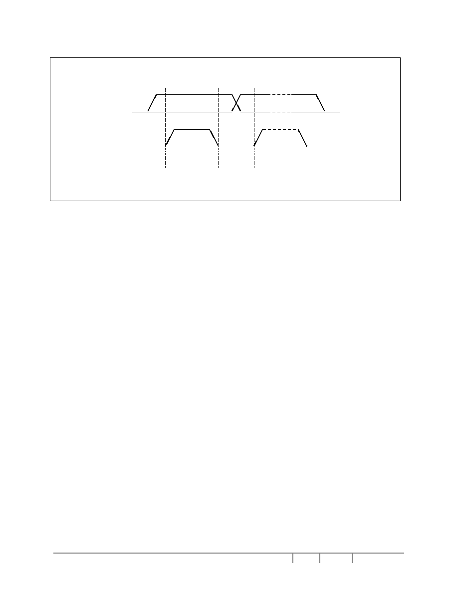
C-bus Write data and read register status
The I
2
C-bus interface gives access to write data and command into the device. Please refer to Figure 8
for the write mode of I
2
C-bus in chronological order.
Figure 8 - I
2
C-bus data format
Write mode
1) The master device initiates the data communication by a start condition. The definition of the start
condition is shown in Figure 9. The start condition is established by pulling the SDA from high to
low while the SCL stays high.
2) The slave address is following the start condition for recognition use. For the SSD0852, the slave
address is either "b0111100" or "b0111101" by changing the SA0 to high or low.
3) The write mode is established by setting the R/W bit to logic "0".
4) An acknowledgement signal will be generated after receiving one byte of data, including the slave
address and the R/W bit. Please refer to the Figure 10 for the graphical representation of the
acknowledge signal. The acknowledge bit is defined as that the SDA line is pulled down during
the high period of the acknowledgement related clock pulse.
5) After the transmission of the slave address, either the control byte or the data byte may be sent
across the SDA. A control byte mainly consists of Co and D/C bits following by six "0" `s.
a. If the Co bit is set as logic "0", the transmission of the following information will contain
data bytes only.
0 1 1 1 1 0
SA0
P
Slave Address
m 0 words
n 0 bytes
MSB ...................LSB
1 byte
Write mode
Slave Address
SSD0852
Slave Address
Read mode
R/
W
D/
C
Co
A
CK
A
CK
Control byte
Data byte
A
CK
Co
D/
C
Control byte
A
CK
Data byte
A
CK
S
0 1 1 1 1 0
0 1 1 1 1 0
S
SA0
A
CK
Status bytes
A
CK
P
SA0
R/
W
Co
D/
C
A
CK
Control byte
Note:
Co � Continuation bit
D/C � Data / Command Selection bit
ACK � Acknowledgement
SA0 � Slave address bit
R/W � Read / Write Selection bit
S � Start Condition / P � Stop Condition
0 0 0 0 0 0
0 1 1 1 1 0
R/
W
SSD0852
Rev 1.0
P 23/44 Feb 2003
Solomon Systech
DATA OUTPUT
BY RECEIVER
DATA OUTPUT
BY TRANSMITTER
SCL FROM
MASTER
S
START
Condition
Clock pulse for
acknowledgement
1
8
9
Non-acknowledge
2
Acknowledge
S
START condition
SDA
SCL
P
STOP condition
SDA
SCL
T
DH
,
START
T
DS
,
STOP
b. The D/C bit determines the next data byte is acted as a command or a data. If the D/C bit
is set to logic "0", it defines the following data byte as a command. If the D/C bit is set to
logic "1", it defines the following data byte as a data which will be stored at the GDDRAM.
The GDDRAM column address pointer will be increased by one automatically after each
data write.
6) Acknowledge bit will be generated after receiving each control byte or data byte.
7) The write mode will be finished when a stop condition is applied. The stop condition is also
defined in Figure 9. The stop condition is established by pulling the "SDA in" from low to high
while the "SCL" stays high.
Figure 9 - Definition of the start and stop condition
Figure 10 - Definition of the acknowledgement condition
Please be noted that the transmission of the data bit has some limitations.
1. The data bit, which is transmitted during each SCL pulse, must be kept at a stable state within
the "high" period of the clock pulse. Please refer to the Figure 11 for graphical representations.
Except in start or stop conditions, the data line can be switched only when the SCL is low.
2. Both the data line (SDA) and the clock line (SCL) should be pulled up by external resistors.
Solomon Systech
Feb 2003
P 24/44 Rev 1.0
SSD0852
Figure 11 - Definition of the data transfer condition
Read mode (Read status register)
1) No Read mode in SSD0852 device
Change
of data is
allowed
data line is
stable; data is
valid
SDA
SCL

SSD0852
Rev 1.0
P 25/44 Feb 2003
Solomon Systech
9 COMMAND
DESCRIPTIONS
9.1 Set Lower Column Address
This command specifies the lower nibble of the 7-bit column address of the display data RAM. The
column address will be incremented by each data access after it is pre-set by the MCU and
returning to 0 once overflow (>127).
9.2 Set Upper Column Address
This command specifies the higher nibble of the 7-bit column address of the display data RAM.
The column address will be incremented by each set of data (LSB & MSB) access after it is pre-set
by the MCU and returning to 0 once overflow (>127).
9.3 Set Internal Regulator Resistor Ratio
This command is to enable any one of the eight internal resistor (IRS) settings for different
regulator gains when using internal regulator resistor network (INTRS pin pulled high). The
Contrast Control Voltage Range curves are given in the Figure 5.
9.4 Set Power Control Register
This command turns on/off the various power circuits associated with the chip.
9.5 Set Display Start Line
This command is to set Display Start Line register and to determine starting address of display
RAM. When starting address equals to 0, D
0
of Page 0 is mapped to COM0. When it equals to 1,
D
1
of Page0 is mapped to COM0. The display start line values of 0 to 127 are assigned to Page 0
to 15.
9.6 Set Display Offset
The second command specifies the mapping of display start line (COM0 if display start line register
equals to 0) to one of ROW0-127. This command has no effect on ICONS. COM0 is mapped to
ROW0 after reset.
9.7 Set Multiplex Ratio
This command switches default 128 multiplex mode to any multiplex from 16 to 128, if Icon is
disabled (POR). When Icon is set enable, the corresponding multiplex ratio setting will be mapped
to 17 to 129. The chip pads ROW0-ROW127 will be switched to corresponding COM signal output.
9.8 Set N-line Inversion
Number of line inversion is set by this command for reducing cross-talk noise. 3 to 33-line inversion
operations could be selected. At POR, this operation is disabled. It should be noted that the total
number of mux (including the icon line) should NOT be a multiple of the inversion number (N). Or
else, some lines will not change their polarity during frame change.
9.9 Set LCD Bias
This command is used to select a suitable bias ratio (1/5 to 1/12) required for driving the particular
LCD panel in use. The POR default 1/12 bias.
9.10
Set DC-DC Converter Factor
Internal DC-DC converter factor is set by this command. 3X to 6X multiplying factors could be
selected.

Solomon Systech
Feb 2003
P 26/44 Rev 1.0
SSD0852
9.11 Set Contrast Control Register
This command adjusts the contrast of the LCD panel by changing V
L6
of the LCD drive voltage
provided by the On-Chip power circuits. V
L6
is set with 64 steps (6-bit) contrast control register. It is
a compound commands.
9.12 Set Gray Scale Mode (White/Light Gray/Dark Gray/Black)
Command 88(hex) to 8F(hex) are used to specify the four gray levels' pulse width at the four
possible frames. The four gray levels are called white, light gray, dark gray and black. Each level is
defined by 4 registers for 4 consecutive frames. For example, WA is a 4-bit register to define the
pulse width of the 1
st
frame in White mode. WB is a register for 2
nd
frame in White mode etc. Each
command specifies two registers.
For 4 FRC,
Memory Content
FRAME
1
st
Byte
2
nd
Byte
Gray Mode
1
st
2
nd
3
rd
4
th
0 0
White
WA
WB
WC
WD
0 1
Light
Gray
LA
LB
LC
LD
1 0
Dark
Gray
DA
DB
DC
DD
1 1
Black
BA
BB
BC
BD
For 3 FRC,
Memory Content
FRAME
1
st
Byte
2
nd
Byte
Gray Mode
1
st
2
nd
3
rd
4
th
(No use)
0 0
White
WA
WB
WC
WD
(XX)
0
1
Light Gray
LA
LB
LC
LD (XX)
1
0
Dark Gray
DA
DB
DC
DC (XX)
1 1
Black
BA
BB
BC
BC
(XX)
Example for pure PWM mode:
No. of level
RAM Content
Gray Scale mode and Register (3/4 FRC)
MSB LSB MSB LSB MSB LSB MSB LSB Dark
Mode
Dark
Gray
Mode
Light Gray
Mode
White Mode
15-levels 1 1 1 0 0 1 0 0 F,F,F,F
A,A,A,A 5,5,5,5
0,0,0,0
12-levels 1 1 1 0 0 1 0 0 C,C,C,C 8,8,8,8
4,4,4,4
0,0,0,0
9-levels 1 1 1 0 0 1 0 0 9,9,9,9
6,6,6,6
3,3,3,3
0,0,0,0
LCD panel
display
Example for pure FRC mode:
No. of Frame
RAM Content
Gray Scale mode and Register (15PWM)
MSB LSB MSB LSB MSB LSB MSB LSB Dark
Mode
Dark
Gray
Mode
Light Gray
Mode
White Mode
3-FRC
1 1 1 0 0 1 0 0 F,F,F,F
F,F,0,0 F,0,0,0 0,0,0,0
4-FRC
1 1 1 0 0 1 0 0 F,F,F,F
F,F,F,0 F,0,0,0 0,0,0,0
LCD panel
display

SSD0852
Rev 1.0
P 27/44 Feb 2003
Solomon Systech
9.13 Set PWM and FRC
This command is used to select the number of frames used in frame rate control, and the number
of levels in the pulse width modulation.
9.14 Set Segment Re-map
This command changes the mapping between the display data column address and segment
driver. It allows flexibility in layout during LCD module assembly. Please refer to Figure 6.
9.15 Set Icon Enable
This command enable/disable the Icon display. When Icon display is enabled and page address is
set to Page 16. This is only one way to set the page address to 16. Therefore, when writing data
for icons, ICON control register ON instruction would be used to set the page address to 16.
9.16 Set Entire Display On/Off
This command forces the entire display, including the icon row, to be "ON" regardless of the
contents of the display data RAM. This command has priority over normal/invert display. To
execute this command, Set Display On command must be sent in advance.
9.17 Set Normal/Inverse Display
This command sets the display to be either normal/invert. In normal display, a RAM data of 1
indicates an "ON" pixel. While in invert display, a RAM data of 0 indicates an "ON" pixel. The icon
line is not affected by this command.
9.18 Set Power Save Mode
To force the chip to enter Sleep Mode.
9.19 Start Internal Oscillator
After POR, the internal oscillator is OFF. It should be turned ON by sending this command to the
chip.
9.20 Set Display On/Off
This command turns the display on/off, by the value of the LSB.
9.21 Set Page Address
This command positions the page address to 0 to 15 possible positions in GDDRAM. Please refer
to Figure 6. The Page Address will be incremented automatically after writing the LSB of column
127 and returning to 0 once overflow (page address > 15).
Set Page Address command cannot be used to set the page address to "16". Use ICON control
register ON/OFF command to set the page address to "16".
9.22 Set COM Output Scan Direction
This command sets the scan direction of the COM output allowing layout flexibility in LCD module
assembly.
9.23 Set Modify-Read
This command stops the automatic increment of the column address after read display data. The
column address is still automatic increment due to write display data.
9.24 Exit Power-save Mode
This command releases the chip from either Standby or Sleep Mode and return to normal
operation.
Solomon Systech
Feb 2003
P 28/44 Rev 1.0
SSD0852
9.25 Software Reset
When the RESET instruction is issued, the following parameters are initialized:
Register Default
Value
Descriptions
Page address
0
Column address
0
Display Start Line
0
GDDRAM page 0,D0
Internal Resistor Ratio
0
Gain = 3.45(IR0)
Contrast 20H
FRC, PWM Mode
0
4FRC, 9PWM
White Palette
(0, 0, 0, 0)
Light Gray Palette
(0, 0, 0, 0)
Dark Gray Palette
(9, 9, 9, 9)
Black Palette
(9, 9, 9, 9)
9.26 Exit N-line Inversion
This command releases the chip from N-line inversion mode. The driving waveform will be inverted
once per frame after issuing this command.
9.27 Exit Modify-read
This command releases the modify-read mode and the column address return to its initial value
(before the set modify-read mode is set).
SSD0852
Rev 1.0
P 29/44 Feb 2003
Solomon Systech
EXTENDED COMMANDS
These commands are used, in addition to basic commands, to trigger the enhanced features, on top of
general ones, designed for the chip.
9.28 Set TC value
This command is to set 1 out of 8 different temperature coefficients in order to match various
liquid crystal temperature grades.
9.29 Enable internal oscillator resistor
This command is used to enable/disable the internal oscillator. The value of the internal
oscillator resistor is 520k
.
9.30 Enable Frame Frequency setting
This command is used to enable/disable the set frame frequency. The frame frequency can be
adjusted when enable internal oscillator resistor and frame frequency setting.
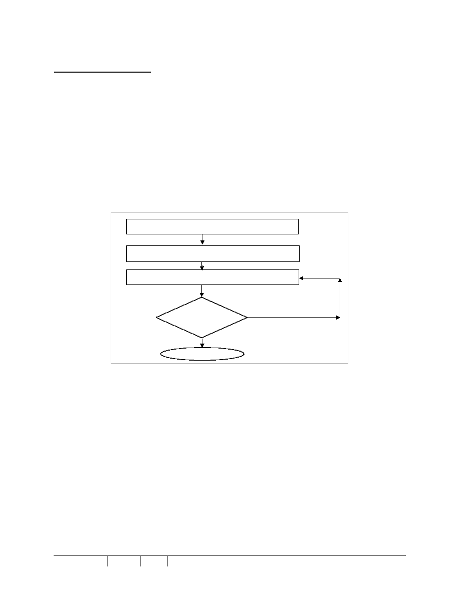
Figure 12 - Sequence for setting frame frequency
Yes
Enable internal oscillator resistor (0xF8; 0XF0)
Enable Frame Frequency setting (0xFB; 0X08)
Set the Frame Frequency (0x82; 0x00~0x70)
END
Accept the
frame
frequency?
NO

Solomon Systech
Feb 2003
P 30/44 Rev 1.0
SSD0852
9.31 Set COM Scan Sequence
This command is used to select one of four sets of COM Scan sequence.
9.32 Set frame frequency
This command specifies the frame frequency so as to minimize the flickering due to the ac main
frequency. The frequency is set to 90Hz(typical) at 128 mux after enabled internal oscillator
resistor.
9.33 OTP setting and programming
OTP (One Time Programming) is a method to adjust V
L6
. In order to eliminate the variations of
LCD module in term of contrast level, OTP can be used to achieve the best contrast of every
LCD modules.
OTP setting and programming should include two major steps of (1) Find the OTP offset and
(2) OTP programming as following,
Step 1. Find OTP offset
(1) Hardware Reset (sending an active low reset pulse to
RES
pin)
(2) Send original initialization routines
(3) Set and display any test patterns
(4) Adjust the contrast value (0x81, 0x00~0x3F) until there is the best visual contrast
(5) OTP setting steps = Contrast value of the best visual contrast - Contrast value of original
initialization
Example 1:
Contrast value of original initialization = 0x20
Contrast value of the best original initialization = 0x24
OTP offset value = 0x24 - 0x20 = +4
OTP setting command should be (0x82, 0x04)
Example 2:
Contrast value of original initialization = 0x20
Contrast value of the best original initialization = 0x1B
OTP setting = 0x1B - 0x20 = -5
OTP setting command should be (0x82, 0x0B)
Step 2. OTP programming
(6) Hardware Reset (sending an active low reset pulse to
RES
pin)
(7) Enable Oscillator (0xAB)
(8) Connect an external V
L6
(see diagram below)
(9) Send OTP setting commands that we find in step 1 (0x82, 0x10~0x1F)
(10) Send OTP programming command (0x83)
(11) Wait at least 2 seconds
(12) Hardware Reset
Verify the result by repeating step 1. (2) � (3)

SSD0852
Rev 1.0
P 31/44 Feb 2003
Solomon Systech
Figure 13 - OTP programming circuitry
R
+
-
SSD0852
V
L6
RES
13.5-14.5V
Note: R = 1K ~ 10k ohm
C = 1u ~ 4.7u F
C
(8)
(1) & (6) & (12)
GND
GND
Solomon Systech
Feb 2003
P 32/44 Rev 1.0
SSD0852
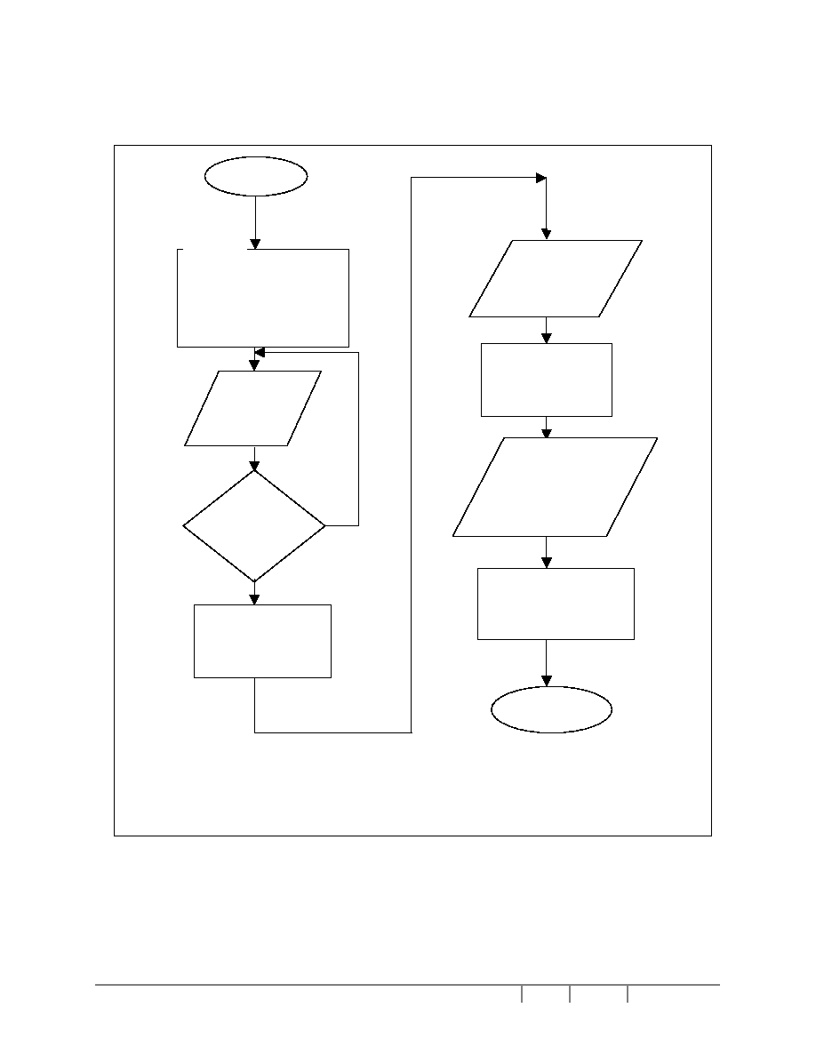
Figure 14 - Flow chart of OTP programming Procedure
Start
OTP setting steps =
Adjusted contrast value
� Original contrast value
Connect an external
voltage (13.5~14.5V)
on V
L6
pins
i) Send original initialization
routines
ii) Set and display any test
patterns
iii) Inspect the contrast
i) Hardware reset
ii) Enable oscillator
END
Yes
No
Adjust the
contrast level
to the best
visual level
Accept the
contrast level
on panel?
i) Send OTP setting
commands
ii) Send OTP programming
command
iii) Wait > 2 sec
iv) Hardware reset
i) Hardware reset
ii) Send original initialization
routines
iii) Set and display any test
patterns
Step 1
Step 2

SSD0852
Rev 1.0
P 33/44 Feb 2003
Solomon Systech
OTP Example program
Find the OTP offset:
1.
Hardware reset by sending an active low reset pulse to
RES
pin
2. COMMAND(0XAB); \\Enable
oscillator;
COMMAND(0X2F);
\\ turn on the internal voltage booster, internal regulator and output op-amp buffer; Select booster
level.
3.
COMMAND(0X48)
\\ Set Duty ratio
COMMAND(0X80) \\
128Mux
COMMAND(0X93)
\\ Set 15 PWM & 4FRC
COMMAND(0X88); COMMAND(0X00) \\ Set white mode
COMMAND(0X89); COMMAND(0X00)
COMMAND(0X8A); COMMAND(0X55) \\ Set light gray mode
COMMAND(0X8B); COMMAND(0X55)
COMMAND(0X8C); COMMAND(0XAA) \\ Set dark gray mode
COMMAND(0X8D); COMMAND(0XAA)
COMMAND(0X8E); COMMAND(0XFF) \\ Set dark mode
COMMAND(0X8F); COMMAND(0XFF)
COMMAND(0X57)
\\ Set Biasing ratio (1/12 BIAS)
4.
COMMAND(0X81)
\\Set target gain and contrast.
COMMAND(0X30)
\\ contrast = 48
COMMAND(0X27)
\\ IR7 => gain = 10.8
5.
\\ Set target display contents
COMMAND(0XB0)
\\ set page address
COMMAND(0x00)
\\ set lower nibble column address
COMMAND(0X10)
\\ set higher nibble column address
DATA(...)
\\ write test pattern to GDDRAM
COMMAND(0XAF)
\\ Set Display ON
6.
OTP offset calculation... target OTP offset value is +3
OTP programming:
7.
Hardware reset by sending an active low reset pulse to
RES
pin
8. COMMAND(0XAB) \\
Enable
Oscillator
9.
Connect a external V
L6
(13.5V~14.5V)
10. COMMAND(0X82)
\\ Set OTP offset value to +3 (0011)
COMMAND(0X03) \\ 0000 X
3
X
2
X
1
X
0
, where X
3
X
2
X
1
X
0
is the OTP offset value
11. COMMAND(0X83)
\\ Send the OTP programming command.
12. Wait at least 2 seconds for programming wait time.
Verify the result:
13. After OTP programming, procedure 2 to 5 are repeated for inspection of the contrast on the panel.

Solomon Systech
Feb 2003
P 34/44 Rev 1.0
SSD0852
9.34 Enable DMA mode
This command enables the DMA mode. The column address will be incremented by each data
access returning to pre-set start column address once overflow (> end column address). The
page address will be incremented by column address overflow. The start column address, end
column address, start page address and end page address should set to 0,127,0,15
respectively before disable DMA mode.
9.35 Set Start/End Column and Page address in DMA mode
This command set the column and page address parameter in DMA mode. The page address
and column address should set to start page address and start column address after set
start/end column and page address.
Figure 15 - Sequence for setting the DMA mode
Figure16 - Sequence for disable the DMA mode
Enable DMA mode (F4H, 05H)
Set Start/End Column and Page address
e.g. 84H, 10H, 01H, 60H, 0CH
(start column address = 16, start page address = 1,
end column address = 96, end page address = 12)
Set page and column address
e.g. B1H, 11H, 00H
(page address = 1, column address = 16)
Available write the data to GDDRAM
Disable DMA mode (F4H, 01H)
Reset Start/End Column and Page address
e.g. 84H, 00H, 00H, 7FH, 0FH
(start column address = 0, start page address = 0,
end column address = 127, end page address = 15)
SSD0852
Rev 1.0
P 35/44 Feb 2003
Solomon Systech
10 MAXIMUM RATINGS
Table 5 - Maximum Ratings (Voltage Reference to V
SS
)
Symbol
Parameter
Value
Unit
V
DD
-0.3 to 4.0
V
V
CC
Supply voltage
-0.3 to 15
V
V
CI
Booster Supply Voltage
-0.3 to 4.0
V
V
in
Input Voltage
-0.3 to V
DD
+ 0.3
V
I
Current Drain Per Pin Excluding V
DD
and V
SS
25 mA
T
A
Operating Temperature
-30 to +85
o
C
T
stg
Storage Temperature Range
-40 to +85
o
C
11 DC CHARACTERISTICS
Table 6 - DC Characteristics
(Unless otherwise specified, Voltage Referenced to V
SS
, V
DD
= 1.8 to 3.3V,
T
A
= -30 to +85
�C)
Symbol
Parameter
Test Condition
Min
Typ
Max
Unit
V
DD
Logic Circuit Supply Voltage
Range
Voltage Generator Circuit Supply
Voltage Range
(Absolute value referenced to V
SS
)
1.8
V
DD
2.7
2.7
3.3
3.3
V
V
I
AC
I
DP1
I
DP2
I
SB
I
SLEEP
Access Mode Supply Current
Drain (V
DD
& V
CI
Pins)
Display Mode Supply Current
Drain (V
DD
& V
CI
Pins)
Display Mode Supply Current
Drain (V
DD
Pins)
Standby Mode Supply Current
Drain (V
DD
Pins)
Sleep Mode Supply Current Drain
(V
DD
Pins)
V
DD
= 2.7V, Voltage Generator On,
6X Converter Endabled,
Write accessing, Tcyc = 3.3MHz,
Osc. Freq.=200kHz, Display On.
V
DD
= 2.7V, V
CC
= 16.2V,
Voltage Generator On,
6X Converter Endabled, Divider
Enabled, Read/Write Halt,
Osc. Freq.=155kHz, Display On,
V
L6
=13V (w/o panel loading)
V
DD
= 2.7V, External VL6 = 13V,
Voltage Generator Off, Divider
Enabled, Read/Write Halt,
Osc. Freq.=155kHz, Display On, V
L6
= 13V.
V
DD
= 2.7V, LCD Driving Waveform
Off, Osc. Freq. 155KHz, Read/Write
halt.
V
DD
= 2.7V, LCD Driving Waveform
Off, Oscillator Off, Read/Write halt.
1
150
10
5
0
1.2
250
15
15
0.1
2
350
30
40
1
mA
�A
�A
�A
�A
V
CC
V
LCD
LCD Driving Voltage Generator
Output (V
CC
Pin)
DC-DC Converter Efficiency
LCD Driving Voltage Input (V
CC
Pin)
Display On, Voltage Generator
Enabled, DC/DC Converter Enabled,
Osc. Freq. = 300kHz, Regulator
Enabled, Divider Enabled.
I
CC
< 80uA
Voltage Generator Disabled.
5.4
95
16.2
98
-
18
100
15
V
%
V
This device contains circuitry to protect the
inputs against damage due to high static
voltages or electric fields; however, it is
advised that normal precautions to be taken
to avoid application of any voltage higher
than maximum rated voltages to this high
impedance circuit. For proper operation it is
recommended that Vin and Vout be
constrained to the range V
SS
< or = (Vin or
V
OUT
) < or = V
DD
. Reliability of operation is
enhanced if unused input are connected to
an appropriate logic voltage level (e.g., either
V
SS
or V
DD
). Unused outputs must be left
open. This device may be light sensitive.
Caution should be taken to avoid exposure of
this device to any light source during normal
operation. This device is not radiation
protected.
* Maximum Ratings are those values beyond which damage to the
device may occur. Functional operation should be restricted to the limits
in the Electrical Characteristics tables or Pin Description section.

Solomon Systech
Feb 2003
P 36/44 Rev 1.0
SSD0852
Symbol
Parameter
Test Condition
Min
Typ
Max
Unit
V
REF
External Reference Voltage Input
Internal Reference Voltage
Internal Reference Voltage Source
Disable (REF pin pulled Low),
External Reference voltage input to
V
EXT
pin [V
REF
= V
EXT
*(1.4/2.1)].
Internal Reference Voltage Source
Enabled (REF pin pulled High), V
EXT
pin NC; (T
A
=25
o
C)
TC0 = -0.05%/
o
C
TC1 = -0.085%/
o
C
TC2 = -0.125%/
o
C (POR)
TC3 = -0.16%/
o
C
TC4 = -0.18%/
o
C
TC5 = -0.21%/
o
C
TC6 = -0.23%/
o
C
TC7 = -0.25%/
o
C
2.06
1.32
1.33
1.37
1.35
1.34
1.36
1.36
1.38
2.1
1.35
1.36
1.40
1.38
1.37
1.39
1.39
1.41
2.14
1.38
1.39
1.43
1.41
1.40
1.42
1.42
1.44
V
V
V
V
V
V
V
V
V
OH1
V
OL1
V
L6
V
L6
Output High voltage (SCL)
Output Low Voltage (SCL)
LCD Driving Voltage Source (V
L6
Pin)
LCD Driving Voltage Source (V
L6
Pin)
Iout = +500
�A
Iout = -500
�A
Regulator Enabled (VL6 voltage
depends on Int/Ext Contrast Control)
Regulator Disable
0.8*V
DD
0.0
V
DD
-
-
-
-
Floating
V
DD
0.2*V
DD
V
CC
-0.5
-
V
V
V
V
V
IH1
V
IL1
Input high voltage
(
RES
, TEST_IN0~TEST_IN6, SCL,
SDA, REF, INTRS)
Input Low voltage
(
RES
, TEST_IN0~TEST_IN6, SCL,
SDA, REF, INTRS)
0.8*V
DD
0.0
-
-
V
DD
0.2*V
DD
V
V
V
L6
V
L5
V
L4
V
L3
V
L2
V
L6
V
L5
V
L4
V
L3
V
L2
LCD Display Voltage Output
(V
L6
, V
L5
, V
L4
, V
L3
, V
L2
Pins)
LCD Display Voltage Input
(V
L6
, V
L5
, V
L4
, V
L3
, V
L2
Pins)
Bias Divider Enabled, 1:a bias ratio,
a=5~12 .
Voltage reference to V
SS
, External
Voltage Generator, Type A and Type
B Bias Divider Disabled
-
-
-
-
-
V
L5
V
L4
V
L3
V
L2
V
SS
V
L6
(a-1)/a*V
L6
(a-2)/a*V
L6
2/a*V
L6
1/a*V
L6
-
-
-
-
-
-
-
-
-
-
V
CC
V
L6
V
L5
V
L4
V
L3
V
V
V
V
V
V
V
V
V
V
I
OH
I
OL
I
OZ
Output High Current Source(D
0
-D
7
)
Output Low Current Drain (D
0
-D
7
)
Output Tri-state Current Drain
Source (D
0
-D
7
)
Vout=V
DD
-0.4V
Vout=0.4V
50
-
-1
-
-
-
-
-50
1
�A
�A
�A
I
IL
/I
IH
Input Current
(
RES
, TEST_IN0~TEST_IN6, SCL,
SDA, REF, INTRS)
-1
1
�A
C
IN
Input Capacitance
(all logic pins)
5
7.5
pF
V
L6
Variation of VL6 Output (1.8V <
V
DD
< 3.3V)
Regulator Enabled, Internal Contrast
Control Enabled, Set Contrast
Control Register = 0
-2% - +2%
%
SSD0852
Rev 1.0
P 37/44 Feb 2003
Solomon Systech
Symbol
Parameter
Test Condition
Min
Typ
Max
Unit
PTC0
PTC1
PTC2
PTC3
PTC4
PTC5
PTC6
PTC7
Temperature Coefficient
Compensation
Flat Temperature Coefficient
Temperature Coefficient 1*
Temperature Coefficient 2* [POR]
Temperature Coefficient 3*
Temperature Coefficient 4*
Temperature Coefficient 5*
Temperature Coefficient 6*
Temperature Coefficient 7*
Voltage Regulator Enabled
Voltage Regulator Enabled
Voltage Regulator Enabled
Voltage Regulator Enabled
Voltage Regulator Enabled
Voltage Regulator Enabled
Voltage Regulator Enabled
Voltage Regulator Enabled
0
-0.075
-0.115
-0.15
-0.175
-0.20
-0.22
-0.24
-0.05
-0.085
-0.125
-0.16
-0.18
-0.21
-0.23
-0.25
-0.06
-0.095
-0.135
-0.175
-0.19
-0.22
-0.24
-0.26
%/
o
C
%/
o
C
%/
o
C
%/
o
C
%/
o
C
%/
o
C
%/
o
C
%/
o
C
*The formula for the temperature coefficient is:
%
100
*
25
1
*
0
50
0
50
)
/
(%
0
0
0
0
0
0
C
at
V
C
C
C
at
V
C
at
V
C
TC
ref
ref
ref
-
-
=
Solomon Systech
Feb 2003
P 38/44 Rev 1.0
SSD0852
12 AC CHARACTERISTICS
Table 7 - AC Characteristics
(Unless otherwise specified, Voltage Referenced to V
SS
, V
DD
= 1.8 to 3.3V,
T
A
= -30 to +85
�C)
Symbol
Parameter Test
Condition
Min
Typ
Max
Unit
F
OSC
Oscillation Frequency of Display
Timing Generator
Internal Oscillator Enabled
Set 128 x 128, Icon Line
Disabled, 15 PWM, oscillator
resistor = 680k
,
V
DD
=2.775V
Internal Oscillator resistor
Enabled, set 128 x 128, Icon
Line Disabled, 15 PWM,
V
DD
=2.775V, Frame frequency
setting (F
2
F
1
F
0
=000)
129.6
147
144
175.5
158.4
199
KHz
KHz
F
FRM
Frame Frequency
Display ON, Set 128 x 128
Graphic Display Mode, Icon
Line Disabled, 9/12/15 PWM,
oscillator resistor = 680k
,
V
DD
=2.775V
Display ON, Set 128 x 128
Graphic Display Mode, Icon
Line Disabled, 15 PWM,
Internal oscillator resistor
enabled,
V
DD
=2.775V, Frame
frequency setting
(F
2
F
1
F
0
=000)
67.5
76.5
75
90
82.5
103.5
Hz
Hz
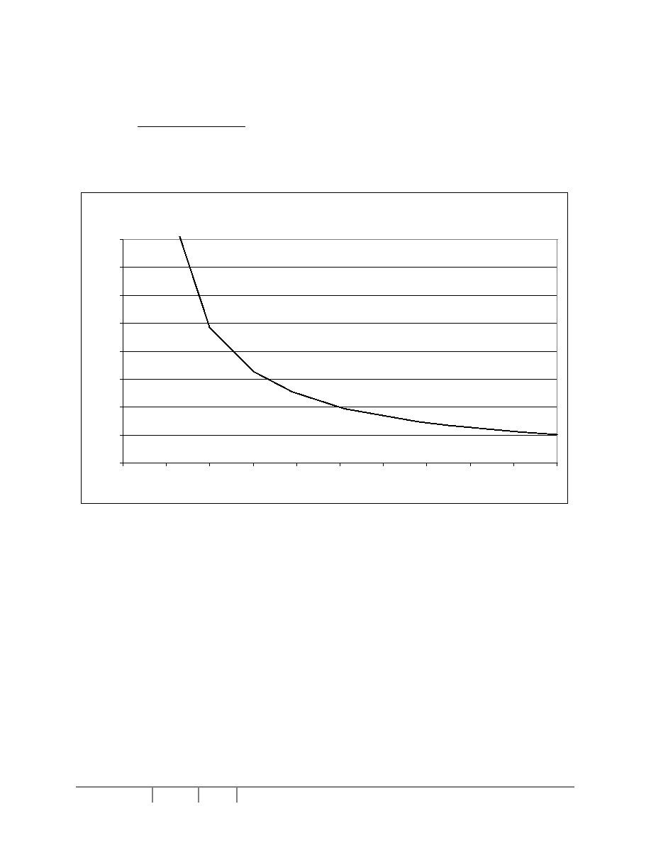
SSD0852
Rev 1.0
P 39/44 Feb 2003
Solomon Systech
The formula for the Frame Frequency is:
*
* PWM
Mux
F
F
OSC
FRM
=
* PWM is the number of level of pulse width modification.
Remarks: F
OSC
will be fine tuned automatically, while change Mux. Therefore, the frame frequency always
within +/- 10Hz of the target frame frequency.
Figure 17 - Relationship between Frame Frequency and Oscillator resistor (TA=25
o
C, V
DD
=2.775V)
Frame Frequency Vs Oscillator Resistor
0
50
100
150
200
250
300
350
400
0
100
200
300
400
500
600
700
800
900
1000
Resistor [k ohm]
Freq [H
z
]
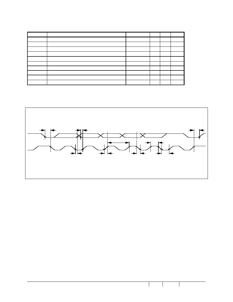
Solomon Systech
Feb 2003
P 40/44 Rev 1.0
SSD0852
Symbol Parameter
Min Typ
Max
Unit
F
SCL
I
2
C-bus Clock frequency, SCL
0
-
400 kHz
T
CLKL
I
2
C-bus Clock Low period, SCL
1.3
-
-
�s
T
CLKH
I
2
C-bus Clock high period, SCL
0.6
-
-
�s
T
DSW
I
2
C-bus Data Setup time, SDA
100
-
-
�s
T
DHW
I
2
C-bus Data Hold time, SDA
0.3
-
0.9
�s
T
R
Rise time between SDA & SCL
20+0.1C
BUS
-
300 ns
T
F
Fall time between SDA & SCL
20+0.1C
BUS
-
300 ns
C
BUS
Capacitive loadings at each I
2
C-bus channel -
-
400 pF
T
DH, START
I
2
C-bus Hold time, START condition
0.6
-
-
�s
T
DS, STOP
I
2
C-bus Setup time, STOP condition
0.6
-
-
�s
Table 8 - I
2
C-bus timing Characteristics
(Unless otherwise specified, Voltage Referenced to V
SS
, V
DD
=
1.8 to 3.3V, T
A
=-30 to +85
�C)
Figure 18 - I
2
C data bus Interface driving waveform
T
DH, START
T
DS, STOP
T
DSW
T
DHW
T
R
T
F
T
CLKH
T
CLKL
T
Cycle
SDA
SCL
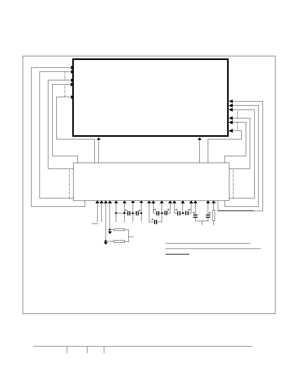
SSD0852
Rev 1.0
P 41/44 Feb 2003
Solomon Systech
13 APPLICATION EXAMPLES
Figure 19 - Typical Application
Logic pin connections not specified above:
Pins connected to V
DD
: TEST_IN_0;REF; INTRS
Pins connected to V
SS
: TEST_IN1~TEST_IN6
SEG127.................................................................................SEG0
DISPLAY PANEL SIZE
128 X 128 + 1 ICON LINE
COM0
:
:
:
:
COM62
COM63
COM64
COM65
:
:
:
COM127
ICONS
SEG0
..............................................................
SEG127
Remapped COM
SCAN Direction
[Command: C8
R
e
mapped C
O
M
S
C
A
N
D
i
r
ecti
on
[C
ommand: C
8
Remapped COM
SCAN Direction
[Command: C8]
:
:
:
:
:
:
:
:
:
:
ROW0
ICONS
SDA
C1....C5
V
SS
SCL
V
CI
V
DD
Segment Remapped
[Command: A1)
SSD0852 IC
128 MUX
(DIE FACE IP)
where V
DD
&V
CI
=2.775V,
Slave address = 0111100,
C1~C5 = 0.47uF~2.0uF,
C6~C12 = 1uF~4.7uF,
R3~R4 = 1K
~5k,
R
OSC
= 680k
V
SS
R
e
mapped C
O
M
S
C
A
N
D
i
r
ecti
on
[C
ommand: C
8
:
:
:
:
:
:
: : : :
ROW6
5
ROW6
4
V
OU
T
:
ROW6
0
ROW6
3
: :
R
O
W
127
ICONS
......
V
L6
:
:
V
L2
C
4P
C
2N
C
2P
C
1P
C
1N
C
3P
C
5P
V
OU
T
V
SS
V
CI
V
DD
SD
A
SC
L
SD
0
/R
ES
V
SS
C6
C7
C8
C9 C10
C12 C11
V
DD
R4
R3
V
DD
R
OSC
Remarks: For noise protection, the wiring
length form OSC1 to Rosc should be minimize
& shielding.
RES

Solomon Systech
Feb 2003
P 42/44 Rev 1.0
SSD0852
14 APPENDIX
14.1 TAB Drawing
Figure 20 - TAB Drawing 1
SS
D0
85
2T
SO
LO
M
ON
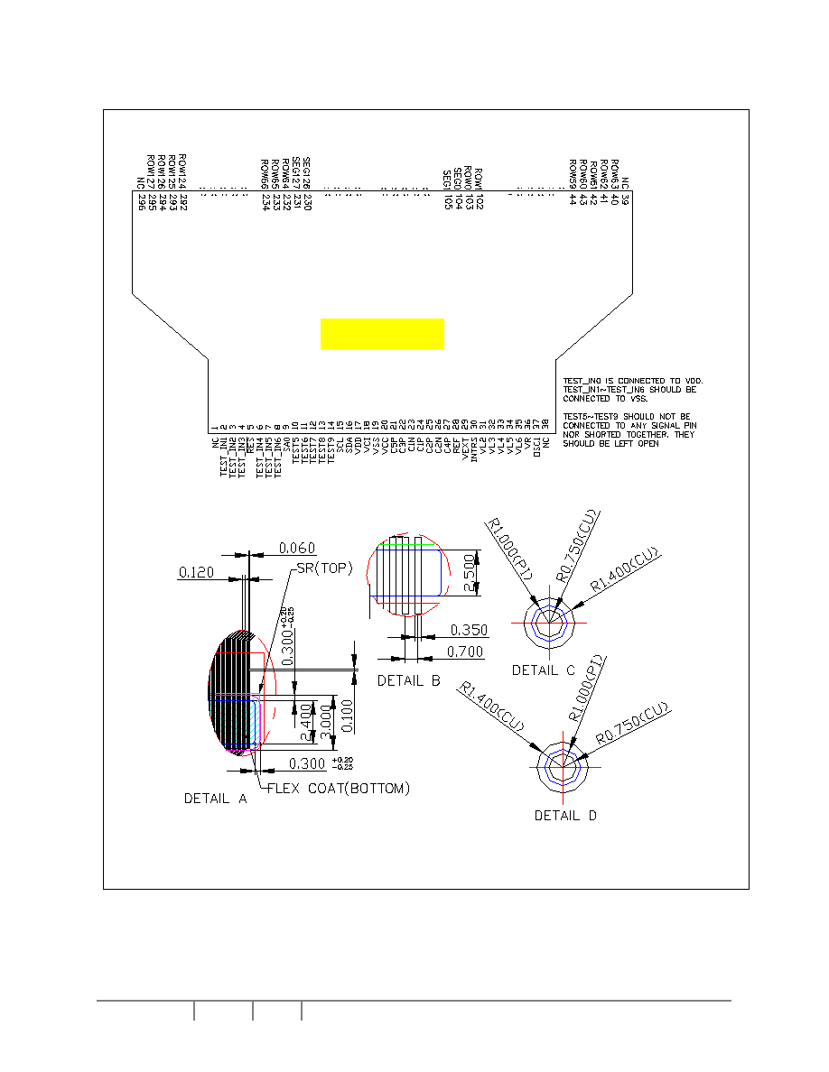
SSD0852
Rev 1.0
P 43/44 Feb 2003
Solomon Systech
Figure 21 - TAB Drawing 2

Solomon Systech
Feb 2003
P 44/44 Rev 1.0
SSD0852
Solomon Systech reserves the right to make changes without further notice to any products herein. Solomon Systech makes no warranty,
representation or guarantee regarding the suitability of its products for any particular purpose, nor does Solomon Systech assume any liability arising
out of the application or use of any product or circuit, and specifically disclaims any and all liability, including without limitation consequential or
incidental damages. "Typical" parameters can and do vary in different applications. All operating parameters, including "Typicals" must be validated for
each customer application by customer's technical experts. Solomon Systech does not convey any license under its patent rights nor the rights of
others. Solomon Systech products are not designed, intended, or authorized for use as components in systems intended for surgical implant into the
body, or other applications intended to support or sustain life, or for any other application in which the failure of the Solomon Systech product could
create a situation where personal injury or death may occur. Should Buyer purchase or use Solomon Systech products for any such unintended or
unauthorized application, Buyer shall indemnify and hold Solomon Systech and its offices, employees, subsidiaries, affiliates, and distributors harmless
against all claims, costs, damages, and expenses, and reasonable attorney fees arising out of, directly or indirectly, any claim of personal injury or
death associated with such unintended or unauthorized use, even if such claim alleges that Solomon Systech was negligent regarding the design or
manufacture of the part.
http://www.solomon-systech.com