
SOLOMON SYSTECH
SEMICONDUCTOR TECHNICAL DATA
This document contains information on a new product. Specifications and information herein are subject to change
without notice.
http://www.solomon-systech.com
SSD1805 Series
Rev 1.1
P 1/52
Jun 2004
Copyright
2004 Solomon Systech Limited
Advance Information
132 x 68 STN
LCD Segment / Common Monochrome Driver with Controller
SSD1805

Solomon Systech
Jun 2004
P 2/52
Rev 1.1
SSD1805 Series
TABLE OF CONTENTS
1
GENERAL DESCRIPTION....................................................................................................................... 5
2
FEATURES............................................................................................................................................... 5
3
ORDERING INFORMATION .................................................................................................................... 5
4
BLOCK DIAGRAM ................................................................................................................................... 6
5
DIE PAD FLOOR PLAN........................................................................................................................... 7
6
PIN DESCRIPTION ................................................................................................................................ 11
7
FUNCTIONAL BLOCK DESCRIPTIONS .............................................................................................. 16
8
COMMAND TABLE................................................................................................................................ 24
9
COMMAND DESCRIPTIONS................................................................................................................. 28
10
MAXIMUM RATINGS ............................................................................................................................. 36
11
DC CHARACTERISTICS ....................................................................................................................... 37
12
AC CHARACTERISTICS ....................................................................................................................... 39
13
APPLICATION EXAMPLES................................................................................................................... 46
14
PACKAGE INFORMATION ................................................................................................................... 49

SSD1805 Series
Rev 1.1
P 3/52
Jun 2004
Solomon Systech
TABLE OF TABLES
Table 1 - Ordering Information ............................................................................................................................ 5
Table 2 - SSD1805 Series Bump Die Pad Coordinates (Bump center) .............................................................. 8
Table 3 - Arrangement of common at different multiplex modes ...................................................................... 15
Table 4 - Data Bus selection Modes.................................................................................................................. 17
Table 5 - Graphic Display Data RAM (GDDRAM) Address Map with Display Start Line set to 18h................. 18
Table 6 - Gain Setting........................................................................................................................................ 20
Table 7 - Temperature compensation coefficient .............................................................................................. 20
Table 8 - Command Table................................................................................................................................. 24
Table 9 - Extended Command Table................................................................................................................. 26
Table 10 - Read Command Table ..................................................................................................................... 27
Table 11 - Automatic Address Increment .......................................................................................................... 28
Table 12 - ROW pin assignment for COM signals for SSD1805 in an 68 MUX display ................................... 35
Table 13 - Maximum Ratings............................................................................................................................. 36
Table 14 - DC Characteristics ........................................................................................................................... 37
Table 15 - AC Characteristics............................................................................................................................ 39
Table 16 - Parallel 6800-series Interface Timing Characteristics...................................................................... 40
Table 17 - Parallel 6800-series Interface Timing Characteristics...................................................................... 41
Table 18 - Parallel 8080-series Interface Timing Characteristics...................................................................... 42
Table 19 - Parallel 8080-series Interface Timing Characteristics...................................................................... 43
Table 20 - 4-wires Serial Interface Timing Characteristics................................................................................ 44
Table 21 - 4-wires Serial Interface Timing Characteristics................................................................................ 45

Solomon Systech
Jun 2004
P 4/52
Rev 1.1
SSD1805 Series
TABLE OF FIGURES
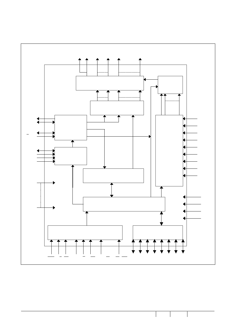
Figure 1 - SSD1805 Block Diagram.....................................................................................................................................6
Figure 2 - SSD1805 Die Pad Floor Plan...............................................................................................................................7
Figure 3 - Display Data Read with the insertion of dummy read .......................................................................................16
Figure 4 - SSD1805 Hardware configuration .....................................................................................................................19
Figure 5 - Contrast curve ....................................................................................................................................................21
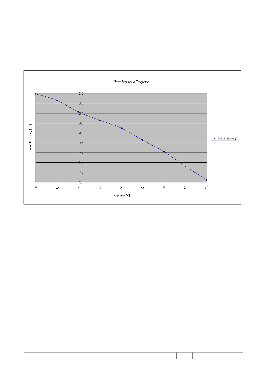
Figure 6 - TC 0 oscillator typical frame frequency with variation in temperature..............................................................22
Figure 7 - LCD Driving Waveform ....................................................................................................................................23
Figure 8 - Contrast Control Flow........................................................................................................................................29
Figure 9 - OTP programming circuitry...............................................................................................................................31
Figure 10 - Flow chart of OTP programming Procedure....................................................................................................32
Figure 11 - Parallel 6800-series Interface Timing Characteristics (P/S = H, C68/80 = H).................................................40
Figure 12 - Parallel 6800-series Interface Timing Characteristics (P/S = H, C68/80 = H).................................................41
Figure 13 - Parallel 8080-series Interface Timing Characteristics (P/S = H, C68/80 = L) .................................................42
Figure 14 - Parallel 8080-series Interface Timing Characteristics (P/S = H, C68/80 = L) .................................................43
Figure 15 - 4-wires Serial Interface Timing Characteristics (P/S = L, C68/80 = L)...........................................................44
Figure 16 - 4-wires Serial Interface Timing Characteristics (P/S = L, C68/80 = L)...........................................................45
Figure 17 - Application Example I (4-wires SPI mode) .....................................................................................................46
Figure 18 - Application Example II (6800 PPI mode)........................................................................................................47
Figure 19 - Applications notes for V
DD
/V
DDIO
connection..................................................................................................48
Figure 20 - SSD1805TR1 TAB Drawing (Copper view) ...................................................................................................50
Figure 21 - SSD1805TR1 TAB Drawing (Detail view & pin assignment) ........................................................................51

SSD1805 Series
Rev 1.1
P 5/52
Jun 2004
Solomon Systech
1 General
Description
SSD1805 is a single-chip CMOS LCD driver with controller for dot-matrix graphic liquid crystal display system.
SSD1805 consists of 200 high-voltage driving output pins for driving maximum 132 Segments, 68 Commons /
132 Segments, 64 Commons and 1 icon-driving Common / 132 Segments, 54 Commons and 1 icon-driving
Common / 132 Segments, 32 Commons and 1 icon-driving Common. SSD1805 can also be switched among
32, 54, 64 or 68 display multiplex ratios by hardware pin selection.
SSD1805 consists of 132 x 68 bits Graphic Display Data RAM (GDDRAM). Data/Commands are sent from
common MCU through 8-bit 6800-series / 8080-series compatible Parallel Interface or 4-wires Serial
Peripheral Interface by software program selections.
SSD1805 embeds DC-DC Converter, On-Chip Oscillator and Bias Divider to reduce the number of external
components. With the advance design, low power consumption, stable LCD operating voltage and flexible die
package layout, SSD1805 is suitable for any portable battery-driven applications requiring long operation
period with compact size.
2 FEATURES
� Power Supply: V
DD
= 1.8V � 3.6V
V
DDIO
= 1.8V � 3.6V
V
CI
= 1.8V � 3.6V
� LCD Driving Output Voltage: V
LCD
= +12.5V
� Low Current Sleep Mode
� Pin selectable 68/64/54/32 multiplex ratio configuration. Maximum display size:
o
132 columns by 68 rows
o
132 columns by 64 rows with one icon line
o
132 columns by 54 rows with one icon line
o
132 columns by 32 rows with one icon line
� 8-bit 6800-series / 8080-series Parallel Interface, 4-wires Serial Peripheral Interface
� On-Chip 132 X 68 = 8976 bits Graphic Display Data RAM
� Column Re-mapping and RAM Page scan direction control
� Vertical Scrolling by Common
� On-Chip Voltage Generator or External LCD Driving Power Supply Selectable
� Pin selectable 2X/3X/4X/5X On-Chip DC-DC Converter with internal flying capacitors.
� 64 Levels Internal Contrast Control
� Programmable LCD Driving Voltage Temperature Compensation Coefficients
� On-Chip Bias Divider with internal compensation capacitors (except V
OUT
)
� Programmable multiplex ratio: 1/9 to 1/68
� Programmable bias ratio: 1/4, 1/5, 1/6, 1/7, 1/8, 1/9
� Display Offset Control
� Non-Volatile Memory (OTP) for calibration
3 ORDERING INFORMATION
Ordering Part Number
SEG COM
Package Form
Reference
Remark
SSD1805Z 132
64/54/32 +
1 icon or
68
Gold Bump Die
Figure 2 on
Page 7
-
SSD1805TR1
132
64 + 1 icon
TAB
Figure 20 on
page 50
-
Table 1 - Ordering Information
Solomon Systech
Jun 2004
P 6/52
Rev 1.1
SSD1805 Series
4 BLOCK
DIAGRAM
Figure 1 - SSD1805 Block Diagram
MSTAT
M/
S
CL
HV Buffer Cell Level Shifter
Display Data Latch
ICONS ROW0 SEG0 ~ SEG131
~ ROW67
Level
Selector
Display
Timing
Generator
Oscillator
GDDRAM
132 x 68 bits
Command Decoder
Command Interface
Parallel/Serial Interface
RES P/ S CS 1 CS2 D
/
C E
(
RD
)
C68/( 80 ) R/
W ( WR )
D7
D6 D5 D4 D3 D2 D1
D0
(SDA) (SCK)
M
/DOF
CLS
C0
C1
V
SS
V
DD
IRS
V
OUT
LCD Driving
Voltage
Generator
2X/3X/4X/5X
Regulated
DC/DC
Converter,
Contrast
Control, Bias
Divider,
Temperature
Compensation
TEST0
B0
B1
V
CI
V
LREF
V
HREF
V
F
V
DDIO
V
SS1
TEST22
V
FS
SSD1805 Series
Rev 1.1
P 7/52
Jun 2004
Solomon Systech
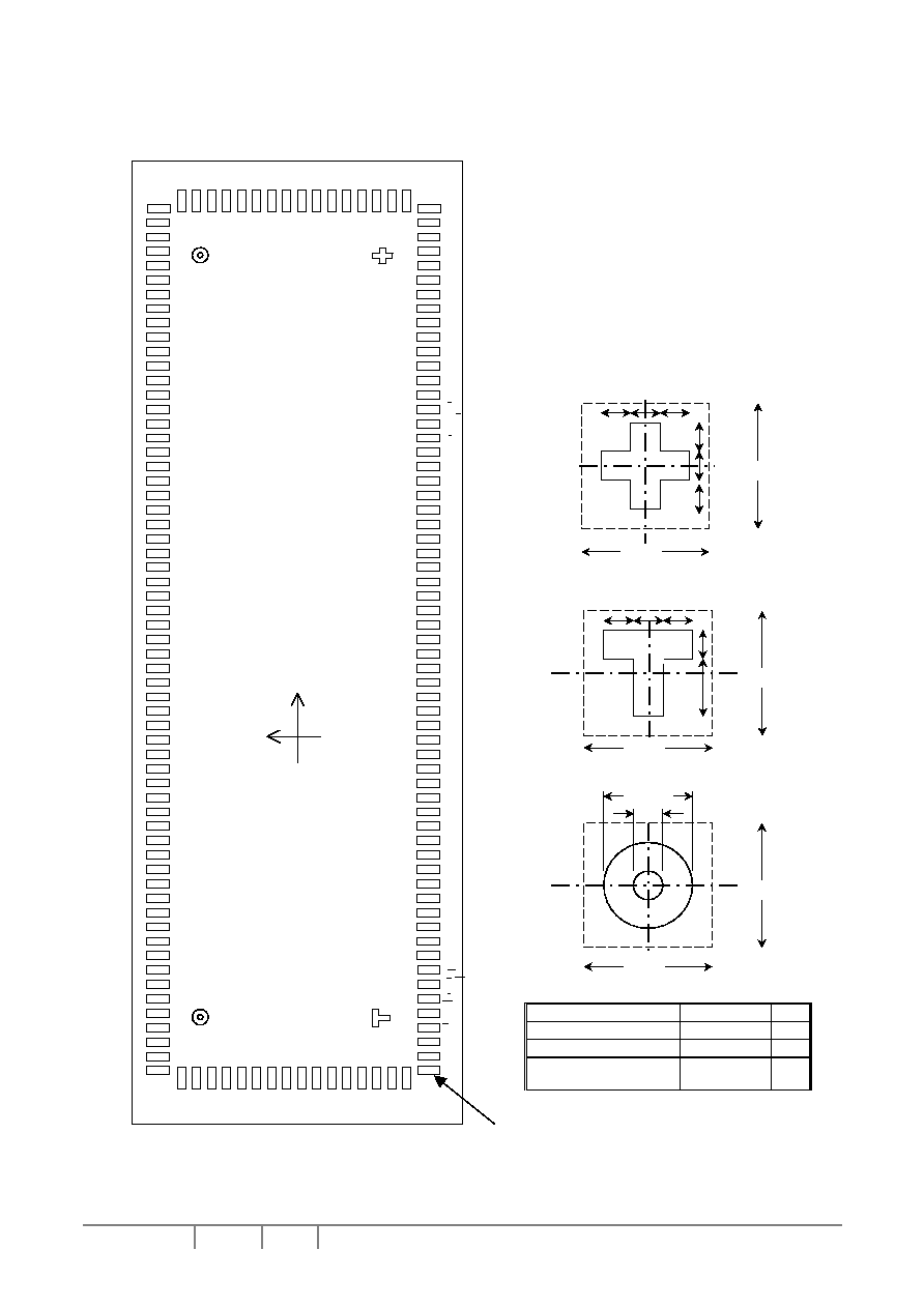
5 DIE PAD FLOOR PLAN
Figure 2 - SSD1805 Die Pad Floor Plan
18
100
75
100
25
25
25
25
25
25
100
100
25
25
25
25
50
100
100
Die Size
11.06 X 1.21 mm
2
Die Thickness
533�25
�m
Typical Bump Height
18
�m
Bump Co-planarity
(within die)
< 3
�m
Note:
1. Diagram showing the die face up.
2. Coordinates are reference to center of the chip.
3. Unit of coordinates and Size of all alignment
marks are in um.
4. All alignment keys do not contain gold bump.
PIN1
NC
TEST22
TEST21
TEST20
TEST19
TEST18
TEST17
TEST16
TEST15
TEST14
TEST13
TEST12
TEST11
TEST10
TEST9
TEST8
TEST7
TEST6
V
DD
B0
V
SS
B1
V
DD
C0
V
SS
C1
V
DD
IRS
V
SS
/HPM
V
DD
P/ S
C68/(
80
)
V
SS
CLS
M/
S
V
DD
V
F
V
OUT
TEST5
TEST4
TEST3
TEST2
TEST1
V
DD
V
FS
V
FS
V
SS
V
OUT
V
OUT
V
OUT
V
OUT
V
OUT
V
OUT
V
OUT
V
OUT
V
OUT
V
OUT
V
OUT
V
OUT
V
OUT
V
HREF
V
HREF
V
CI
V
CI
V
SS1
V
SS1
V
SS1
V
SS1
V
SS1
V
SS1
V
SS1
V
SS1
V
SS1
V
SS1
V
SS1
V
SS1
V
SS1
V
SS
V
SS
V
SS
V
SS
V
SS
V
SS
V
SS
V
SS
V
SS
V
SS
V
LREF
V
LREF
V
CI
V
CI
V
CI
V
CI
V
CI
V
CI
V
CI
V
CI
V
CI
V
CI
V
CI
V
CI
V
CI
V
DD
V
DD
V
DD
V
DD
V
DD
V
DD
V
DDIO
V
DDIO
D7 (SDA)
D6 (SCK)
D5
D4
D3
D2
D1
D0
V
DD
E(
RD
)
R/
W
(
WR
)
V
SS
D/
C
RES
V
DD
CS2
CS
1
V
SS
/DOF
CL
M
MSTAT
TEST0
NC
0,0
Y
X
Cent
r
e
:
5103,
-
236
Cent
r
e
:
-
5103,
195
Cent
r
e
:
5103,
195
Cent
r
e
:
-
5103,
-
236
NC
R
O
W
67
R
O
W
66
R
O
W
65
:
:
:
:
:
:
:
:
:
:
:
:
:
:
:
:
:
:
:
:
:
:
:
:
:
:
:
R
O
W
58
R
O
W
57
R
O
W
56
NC
NC
R
O
W
22
R
O
W
23
R
O
W
24
:
:
:
:
:
:
:
:
:
:
:
:
:
:
:
:
:
:
:
:
:
:
:
:
:
:
R
O
W
31
R
O
W
32
R
O
W
33
NC
NC
ROW21
ROW20
ROW19
:
:
:
:
:
:
:
:
:
:
:
:
:
:
:
:
:
:
:
:
:
:
:
:
:
:
ROW2
ROW1
ROW0
SEG0
SEG1
SEG2
:
:
:
:
:
:
:
:
;
;
;
;
;
;
;
;
;
:
:
:
:
:
:
:
:
:
:
:
:
:
:
:
;
;
:
;
;
:
:
:
;
;
;
;
;
;
;
;
;
;
;
;
;
:
:
:
;
;
;
;
;
;
:
:
:
:
SEG129
SEG130
SEG131
ROW34
ROW35
ROW36
:
:
:
:
:
:
:
:
:
:
:
:
:
:
:
:
:
:
:
:
:
:
:
:
:
:
:
ROW53
ROW54
ROW55
NC

Solomon Systech
Jun 2004
P 8/52
Rev 1.1
SSD1805 Series
Table 2 - SSD1805 Series Bump Die Pad Coordinates (Bump center)
Pad #
Signal
X-pos
Y-pos
Pad #
Signal
X-pos
Y-pos
Pad #
Signal
X-pos
Y-pos
1
NC -5167.10 -448.50 51
V
SS
-1297.10 -448.50
101 CLS 2517.90
-448.50
2 TEST0
-5035.80 -448.50
52 V
SS
-1220.80 -448.50
102 V
SS
2594.20
-448.50
3 MSTAT
-4959.50 -448.50
53 V
SS
-1144.50 -448.50
103 C68/(
80
) 2670.50 -448.50
4 M
-4883.20 -448.50
54
V
SS
-1068.20 -448.50
104 P/
S
2746.80 -448.50
5 CL
-4806.90 -448.50
55
V
SS
-991.90 -448.50
105 V
DD
2823.10
-448.50
6 /DOF
-4730.60 -448.50
56 V
SS
-915.60 -448.50
106 /HPM
2899.40
-448.50
7 V
SS
-4654.30 -448.50 57
V
SS
-839.30 -448.50
107 V
SS
2975.70
-448.50
8
CS
1
-4578.00 -448.50 58 V
SS1
-763.00 -448.50
108 IRS 3052.00
-448.50
9 CS2
-4501.70 -448.50
59 V
SS1
-686.70 -448.50
109 V
DD
3128.30
-448.50
10 V
DD
-4425.40 -448.50 60 V
SS1
-610.40 -448.50
110 C1 3204.60
-448.50
11
RES
-4349.10 -448.50 61 V
SS1
-534.10 -448.50
111 V
SS
3280.90
-448.50
12
C
/
D
-4272.80 -448.50 62 V
SS1
-457.80 -448.50
112 C0 3357.20
-448.50
13 V
SS
-4196.50 -448.50 63 V
SS1
-381.50 -448.50
113 V
DD
3433.50
-448.50
14
W
/
R
(
WR
) -4120.20 -448.50 64 V
SS1
-305.20 -448.50
114 B1 3509.80
-448.50
15
E(
RD
) -4043.90 -448.50 65 V
SS1
-228.90 -448.50
115 V
SS
3586.10
-448.50
16 V
DD
-3967.60 -448.50 66 V
SS1
-152.60 -448.50
116 B0 3662.40
-448.50
17 D0
-3891.30 -448.50
67 V
SS1
-76.30
-448.50
117 V
DD
3738.70
-448.50
18 D1
-3815.00 -448.50
68 V
SS1
0.00
-448.50
118
TEST6
3815.00
-448.50
19 D2
-3738.70 -448.50
69 V
SS1
76.30
-448.50
119 TEST7
3891.30
-448.50
20 D3
-3662.40 -448.50
70 V
SS1
152.60
-448.50
120 TEST8
3967.60
-448.50
21 D4
-3586.10 -448.50
71 V
CI
228.90
-448.50
121 TEST9
4043.90
-448.50
22 D5
-3509.80 -448.50
72 V
CI
305.20
-448.50
122
TEST10
4120.20
-448.50
23 D6
(SCK)
-3433.50 -448.50 73 V
HREF
381.50
-448.50
123 TEST11
4196.50
-448.50
24 D7
(SDA)
-3357.20 -448.50 74 V
HREF
457.80
-448.50
124 TEST12
4272.80
-448.50
25 V
DDIO
-3280.90 -448.50 75
V
OUT
534.10
-448.50
125 TEST13
4349.10
-448.50
26 V
DDIO
-3204.60 -448.50 76
V
OUT
610.40
-448.50
126 TEST14
4425.40
-448.50
27 V
DD
-3128.30 -448.50 77 V
OUT
686.70
-448.50
127 TEST15
4501.70
-448.50
28 V
DD
-3052.00 -448.50 78 V
OUT
763.00
-448.50
128 TEST16
4578.00
-448.50
29 V
DD
-2975.70 -448.50 79 V
OUT
839.30
-448.50
129 TEST17
4654.30
-448.50
30 V
DD
-2899.40 -448.50 80 V
OUT
915.60
-448.50
130 TEST18
4730.60
-448.50
31 V
DD
-2823.10 -448.50 81 V
OUT
991.90
-448.50
131 TEST19
4806.90
-448.50
32 V
DD
-2746.80 -448.50 82 V
OUT
1068.20 -448.50
132 TEST20
4883.20
-448.50
33 V
CI
-2670.50 -448.50 83 V
OUT
1144.50 -448.50
133 TEST21
4959.50
-448.50
34 V
CI
-2594.20 -448.50 84 V
OUT
1220.80 -448.50
134 TEST22
5035.80
-448.50
35 V
CI
-2517.90 -448.50 85 V
OUT
1297.10 -448.50
135 NC 5167.10
-448.50
36 V
CI
-2441.60 -448.50 86 V
OUT
1373.40 -448.50
136 NC 5372.00
-376.00
37 V
CI
-2365.30 -448.50 87 V
OUT
1449.70 -448.50
137 ROW33
5372.00
-318.00
38 V
CI
-2289.00 -448.50 88 V
SS
1526.00 -448.50
138 ROW32
5372.00
-260.00
39 V
CI
-2212.70 -448.50 89 V
FS
1602.30 -448.50
139 ROW31
5372.00
-202.00
40 V
CI
-2136.40 -448.50 90 V
FS
1678.60 -448.50
140 ROW30
5372.00
-144.00
41 V
CI
-2060.10 -448.50 91 V
DD
1754.90 -448.50
141 ROW29
5372.00
-86.00
42 V
CI
-1983.80 -448.50 92 TEST1
1831.20 -448.50
142 ROW28
5372.00
-28.00
43 V
CI
-1907.50 -448.50 93 TEST2
1907.50 -448.50
143 ROW27
5372.00
30.00
44 V
CI
-1831.20 -448.50 94 TEST3
1983.80 -448.50
144 ROW26
5372.00
88.00
45 V
CI
-1754.90 -448.50 95 TEST4
2060.10 -448.50
145 ROW25
5372.00
146.00
46 V
LREF
-1678.60 -448.50 96 TEST5 2136.40 -448.50
146 ROW24
5372.00
204.00
47 V
LREF
-1602.30 -448.50 97
V
OUT
2212.70 -448.50
147 ROW23
5372.00
262.00
48 V
SS
-1526.00 -448.50 98
V
F
2289.00 -448.50
148 ROW22
5372.00
320.00
49 V
SS
-1449.70 -448.50 99
V
DD
2365.30 -448.50
149 NC 5372.00
378.00
50 V
SS
-1373.40 -448.50 100 M/
S
2441.60 -448.50
150 NC
5141.25
448.50
SSD1805 Series
Rev 1.1
P 9/52
Jun 2004
Solomon Systech
Pad #
Signal X-pos
Y-pos
Pad #
Signal
X-pos
Y-pos
Pad #
Signal X-pos
Y-pos
151 ROW21
5083.25 448.50 201 SEG28
2175.00 448.50
251 SEG78
-725.00
448.50
152 ROW20
5025.25 448.50 202 SEG29
2117.00 448.50
252 SEG79
-783.00
448.50
153 ROW19
4967.25 448.50 203 SEG30
2059.00 448.50
253 SEG80
-841.00
448.50
154 ROW18
4909.25 448.50 204 SEG31
2001.00 448.50
254 SEG81
-899.00
448.50
155 ROW17
4851.25 448.50 205 SEG32
1943.00 448.50
255 SEG82
-957.00
448.50
156 ROW16
4793.25 448.50 206 SEG33
1885.00 448.50
256 SEG83
-1015.00 448.50
157 ROW15
4735.25 448.50 207 SEG34
1827.00 448.50
257 SEG84
-1073.00 448.50
158 ROW14
4677.25 448.50 208 SEG35
1769.00 448.50
258 SEG85
-1131.00 448.50
159 ROW13
4619.25 448.50 209 SEG36
1711.00 448.50
259 SEG86
-1189.00 448.50
160 ROW12
4561.25 448.50 210 SEG37
1653.00 448.50
260 SEG87
-1247.00 448.50
161 ROW11
4503.25 448.50 211 SEG38
1595.00 448.50
261 SEG88
-1305.00 448.50
162 ROW10
4445.25 448.50 212 SEG39
1537.00 448.50
262 SEG89
-1363.00 448.50
163 ROW9
4387.25 448.50 213 SEG40
1479.00 448.50
263 SEG90
-1421.00 448.50
164 ROW8
4329.25 448.50 214 SEG41
1421.00 448.50
264 SEG91
-1479.00 448.50
165 ROW7
4271.25 448.50 215 SEG42
1363.00 448.50
265 SEG92
-1537.00 448.50
166 ROW6
4213.25 448.50 216 SEG43
1305.00 448.50
266 SEG93
-1595.00 448.50
167 ROW5
4155.25 448.50 217 SEG44
1247.00 448.50
267 SEG94
-1653.00 448.50
168 ROW4
4097.25 448.50 218 SEG45
1189.00 448.50
268 SEG95
-1711.00 448.50
169 ROW3
4039.25 448.50 219 SEG46
1131.00 448.50
269 SEG96
-1769.00 448.50
170 ROW2
3981.25 448.50 220 SEG47
1073.00 448.50
270 SEG97
-1827.00 448.50
171 ROW1
3923.25 448.50 221 SEG48
1015.00 448.50
271 SEG98
-1885.00 448.50
172 ROW0
3865.25 448.50 222 SEG49
957.00
448.50
272 SEG99
-1943.00 448.50
173 SEG0
3799.00 448.50
223 SEG50
899.00
448.50
273
SEG100
-2001.00 448.50
174 SEG1
3741.00 448.50
224 SEG51
841.00
448.50
274
SEG101
-2059.00 448.50
175 SEG2
3683.00 448.50
225 SEG52
783.00
448.50
275
SEG102
-2117.00 448.50
176 SEG3
3625.00 448.50
226 SEG53
725.00
448.50
276
SEG103
-2175.00 448.50
177 SEG4
3567.00 448.50
227 SEG54
667.00
448.50
277
SEG104
-2233.00 448.50
178 SEG5
3509.00 448.50
228 SEG55
609.00
448.50
278
SEG105
-2291.00 448.50
179 SEG6
3451.00 448.50
229 SEG56
551.00
448.50
279
SEG106
-2349.00 448.50
180 SEG7
3393.00 448.50
230 SEG57
493.00
448.50
280
SEG107
-2407.00 448.50
181 SEG8
3335.00 448.50
231 SEG58
435.00
448.50
281
SEG108
-2465.00 448.50
182 SEG9
3277.00 448.50
232 SEG59
377.00
448.50
282
SEG109
-2523.00 448.50
183 SEG10
3219.00 448.50 233 SEG60
319.00
448.50
283
SEG110
-2581.00 448.50
184 SEG11
3161.00 448.50 234 SEG61
261.00
448.50
284
SEG111
-2639.00 448.50
185 SEG12
3103.00 448.50 235 SEG62
203.00
448.50
285
SEG112
-2697.00 448.50
186 SEG13
3045.00 448.50 236 SEG63
145.00
448.50
286
SEG113
-2755.00 448.50
187 SEG14
2987.00 448.50 237 SEG64
87.00
448.50
287
SEG114
-2813.00 448.50
188 SEG15
2929.00 448.50 238 SEG65
29.00
448.50
288
SEG115
-2871.00 448.50
189 SEG16
2871.00 448.50 239 SEG66
-29.00
448.50
289
SEG116
-2929.00 448.50
190 SEG17
2813.00 448.50 240 SEG67
-87.00
448.50
290
SEG117
-2987.00 448.50
191 SEG18
2755.00 448.50 241 SEG68
-145.00 448.50
291
SEG118
-3045.00 448.50
192 SEG19
2697.00 448.50 242 SEG69
-203.00 448.50
292
SEG119
-3103.00 448.50
193 SEG20
2639.00 448.50 243 SEG70
-261.00 448.50
293
SEG120
-3161.00 448.50
194 SEG21
2581.00 448.50 244 SEG71
-319.00 448.50
294
SEG121
-3219.00 448.50
195 SEG22
2523.00 448.50 245 SEG72
-377.00 448.50
295
SEG122
-3277.00 448.50
196 SEG23
2465.00 448.50 246 SEG73
-435.00 448.50
296
SEG123
-3335.00 448.50
197 SEG24
2407.00 448.50 247 SEG74
-493.00 448.50
297
SEG124
-3393.00 448.50
198 SEG25
2349.00 448.50 248 SEG75
-551.00 448.50
298
SEG125
-3451.00 448.50
199 SEG26
2291.00 448.50 249 SEG76
-609.00 448.50
299
SEG126
-3509.00 448.50
200 SEG27
2233.00 448.50 250 SEG77
-667.00 448.50
300
SEG127
-3567.00 448.50

Solomon Systech
Jun 2004 P 10/52
Rev 1.1
SSD1805 Series
Pad #
Signal
X-pos
Y-pos
301 SEG128 -3625.00 448.50
302 SEG129 -3683.00 448.50
303 SEG130 -3741.00 448.50
304 SEG131 -3799.00 448.50
305 ROW34 -3865.25 448.50
306 ROW35 -3923.25 448.50
307 ROW36 -3981.25 448.50
308 ROW37 -4039.25 448.50
309 ROW38 -4097.25 448.50
310 ROW39 -4155.25 448.50
311 ROW40 -4213.25 448.50
312 ROW41 -4271.25 448.50
313 ROW42 -4329.25 448.50
314 ROW43 -4387.25 448.50
315 ROW44 -4445.25 448.50
316 ROW45 -4503.25 448.50
317 ROW46 -4561.25 448.50
318 ROW47 -4619.25 448.50
319 ROW48 -4677.25 448.50
320 ROW49 -4735.25 448.50
321 ROW50 -4793.25 448.50
322 ROW51 -4851.25 448.50
323 ROW52 -4909.25 448.50
324 ROW53 -4967.25 448.50
325 ROW54 -5025.25 448.50
326 ROW55 -5083.25 448.50
327 NC -5141.25
448.50
328 NC -5372.00
378.00
329 ROW56 -5372.00 320.00
330 ROW57 -5372.00 262.00
331 ROW58 -5372.00 204.00
332 ROW59 -5372.00 146.00
333 ROW60 -5372.00 88.00
334 ROW61 -5372.00 30.00
335 ROW62 -5372.00 -28.00
336 ROW63 -5372.00 -86.00
337 ROW64 -5372.00 -144.00
338 ROW65 -5372.00 -202.00
339 ROW66 -5372.00 -260.00
340 ROW67 -5372.00 -318.00
341 NC -5372.00
-376.00
Bump Size
PAD#
X [um] Y [um] Pad pitch [um] (Min)
Pad 1
56
92
131.3
Pad 2 - 134
56
92
76.3
Pad 135
56
92
131.3
Pad 136 - 149 89
36
58
Pad 150 - 327 36
89
58
Pad 328 - 341 89
36
58
X
Y
Pad pitch

SSD1805 Series
Rev 1.1
P 11/52
Jun 2004
Solomon Systech
6 PIN
DESCRIPTION
6.1 MSTAT
This pin is the static indicator driving output. The frame signal output pin, M, should be used as the back
plane signal for the static indicator. The duration of overlapping could be programmable. See Extended
Command Table for details.
6.2 M
This pin is the frame signal input/output. In master mode, the pin supplies frame signal to slave devices while
in slave mode, the pin receives frame signal from the master device.
6.3 CL
This pin is the display clock input/output. In master mode with internal oscillator enabled (CLS pin pulled
high), this pin supplies display clock signal to slave devices. In slave mode or when internal oscillator is
disabled, the pin receives display clock signal from the master device or external clock source.
6.4 /DOF
This pin is display blanking control between master and slave devices. In master mode, this pin supplies
on/off signal to slave devices. In slave mode, this pin receives on/off signal from the master device.
6.5
CS
1, CS2
These pins are the chip select inputs. The chip is enabled for MCU communication only when both
CS
1 is
pulled low and CS2 is pulled high.
6.6
RES
This pin is the reset signal input. Initialization of the chip is started once this pin is pulled low. Minimum pulse
width for reset sequence is 20us.
6.7 D/
C
This pin is Data/Command control pin. When the pin is pulled high, the data at D7 - D0 is treated as display
data. When the pin is pulled low, the data at D7 - D0 will be transferred to the command register.
6.8 R/
W
(
WR
)
This pin is MCU interface input. When 6800 interface mode is selected, this pin will be used as Read/Write
(
R/W
) selection input. Read mode will be carried out when this pin is pulled high and write mode when low.
When 8080 interface mode is selected, this pin is the Write (
WR
) control signal input. Data write operation is
initiated when this pin is pulled low and the chip is selected. When serial interface mode is selected, this pin
must be pulled low.
6.9 E(
RD
)
This pin is MCU interface input. When 6800 interface mode is selected, this pin will be used as the Enable (E)
signal. Read/write operation is initiated when this pin is pulled high and the chip is selected. When 8080
interface mode is selected, this pin is the Read (
RD
) control signal input. Data read operation is initiated
when this pin is pulled low and the chip is selected. When serial interface mode is selected, this pin must be
pulled high.
6.10 D7 - D0
These pins are the 8-bit bi-directional data bus in parallel interface mode. D7 is the MSB while D0 is the LSB.
When serial mode is selected, D7 is the serial data input (SDA) and D6 is the serial clock input (SCK).

Solomon Systech
Jun 2004 P 12/52
Rev 1.1
SSD1805 Series
6.11 V
DDIO
This pin is the system power supply pin of bus IO buffer. Please refer to figure 19 on page 48 for connection
example.
6.12 V
DD
This pin is the system power supply pin of the logic block.
6.13 V
CI
Reference voltage input for internal DC-DC converter. The voltage of generated V
OUT
equals to the multiple
factor (2X, 3X, 4X or 5X) times V
CI
with respect to V
SS1
.
Note: Voltage at this input pin must be larger than or equal to V
DD
.
6.14 V
SS
The V
SS
is the ground reference of the system.
6.15 V
SS1
Reference voltage input for internal DC-DC converter. The voltage of generated V
OUT
equals to the multiple
factor (2X, 3X, 4X or 5X) times V
CI
with respect to V
SS1
.
Note: Voltage at this input pin must be equal to V
SS
.
6.16 V
LREF
This pin is the ground of internal operation amplifier. In normal power mode, it must connect to V
SS
. In low
power mode, it must connect to V
CI
. Please refer to figure 19 on page 48 for the detail.
6.17 V
HREF
This pin is the power supply pin of the internal operation amplifier. It must connect to V
OUT
.
6.18 V
OUT
This is the most positive voltage supply pin of the chip. It can be supplied externally or generated by the
internal DC-DC converter. If the internal DC-DC converter generates the voltage level at V
OUT
, the voltage
level is used for internal referencing only. The voltage level at V
OUT
pin is not used for driving external
circuitry.
6.19 V
FS
This is an input pin to provide an external voltage reference for the internal voltage regulator. The function of
this pin is only enabled for the External Input chip models which are required special ordering. For normal
chip model, please leave this pin NC (No connection).
6.20 V
F
This pin is the input of the built-in voltage regulator for generating V
OUT
.
When external resistor network is
selected (IRS pulled low) to generate the LCD driving level, V
OUT
, two external resistors, R
1
and R
2
, should be
connected between V
SS
and V
F
, and V
F
and V
OUT
, respectively (see application circuit diagrams).
6.21 M/
S
This pin is the master/slave mode selection input. When this pin is pulled high, master mode is selected,
which CL, M, MSTAT and /DOF signals will be output for slave devices. When this pin is pulled low, slave
mode is selected, which CL, M, /DOF are required to be input from master device. MSTAT will still be an
output signal in slave mode.
6.22 CLS
This pin is the internal clock enable pin. When this pin is pulled high, internal clock is enabled.
The internal
clock will be disabled when it is pulled low, an external clock source must be input to CL pin for normal opera-
tion.

SSD1805 Series
Rev 1.1
P 13/52
Jun 2004
Solomon Systech
6.23 C68/
80
This pin is MCU parallel interface selection input. When the pin is pulled high, 6800 series interface is
selected and when the pin is pulled low, 8080 series interface is selected.
If Serial Interface is selected (
P/ S
pulled low), the setting of this pin is ignored, but it must be connected to a known logic (either high or low).
6.24 P/
S
This pin is serial/parallel interface selection input. When this pin is pulled high, parallel interface mode is
selected. When it is pulled low, serial interface will be selected.
Note1: For serial mode,
R/W ( WR )
must be connected to Vss. E/(
RD
) must be connected to V
DD
. D0 to D5
and C68/80 can be connected to either V
DD
or V
SS
.
Note2: Read Back operation is only available in parallel mode.
6.25 /HPM
This pin is the control input of High Power Current Mode. The function of this pin is only enabled for High
Power model, which required special ordering. For normal models, High Power Mode is disabled.
Note: This pin must be pulled to high. Leaving this pin floating is prohibited.
6.26 IRS
This is the input pin to enable the internal resistors network for the voltage regulator. When this pin is pulled
high, the internal feedback resistors of the internal regulator for generating V
OUT
will be enabled. When it is
pulled low, external resistors, R
1
and R
2
, should be connected to V
SS
and V
F
, and V
F
and V
OUT
, respectively
(see application circuit diagrams).
6.27 C1, C0
These pins are the Chip Mode Selection input. The chip mode is determined by multiplex ratio. Altogether
there are four chip modes. Please see the following list for reference.
C1 C0 Chip
Mode
0
0
32 MUX Mode
0
1
54 MUX Mode
1
0
64 MUX Mode
1
1
68 MUX Mode
Please refer to Table 3 on page 15 for detail description of common pins at different multiplex mode.
6.28 B1, B0
These pins are the Chip Mode Selection input. The chip mode is determined by default boosting level.
Altogether there are four chip modes. Please see the following list for reference.
B1 B0 Chip
Mode
0
0
3X as POR default
0
1
4X as POR default
1
0
5X as POR default
1
1
2X as POR default
5X, 4X, 3X or 2X booster level can be selected as POR default value of the device.
6.29 ROW0 to ROW67
These pins provide the Common driving signals to the LCD panel. See Table 3 on page 15 for the COM
signal mapping in different multiplex mode of SSD1805. There are ICON pins on the chip when either 64 or
54 or 32 Mux mode is selected. The ICON pins are located at the COM 0 pin and COM 67 pin.
6.30 SEG0 to SEG131
These pins provide the LCD segment driving signals. The output voltage level of these pins is V
SS
during
sleep mode and standby mode.
6.31 TEST0
This pin is a test pin. It is recommended to connect to VSS in normal operation.

Solomon Systech
Jun 2004 P 14/52
Rev 1.1
SSD1805 Series
6.32 TEST1 ~ TEST22
These pins are test pins. Nothing should be connected to these pins, nor they are connected together.
6.33 NC
These pins are NC/no connection pins. Nothing should be connected to these pins, nor they are connected
together.
SSD1805 Series
Rev 1.1
P 15/52
Jun 2004
Solomon Systech
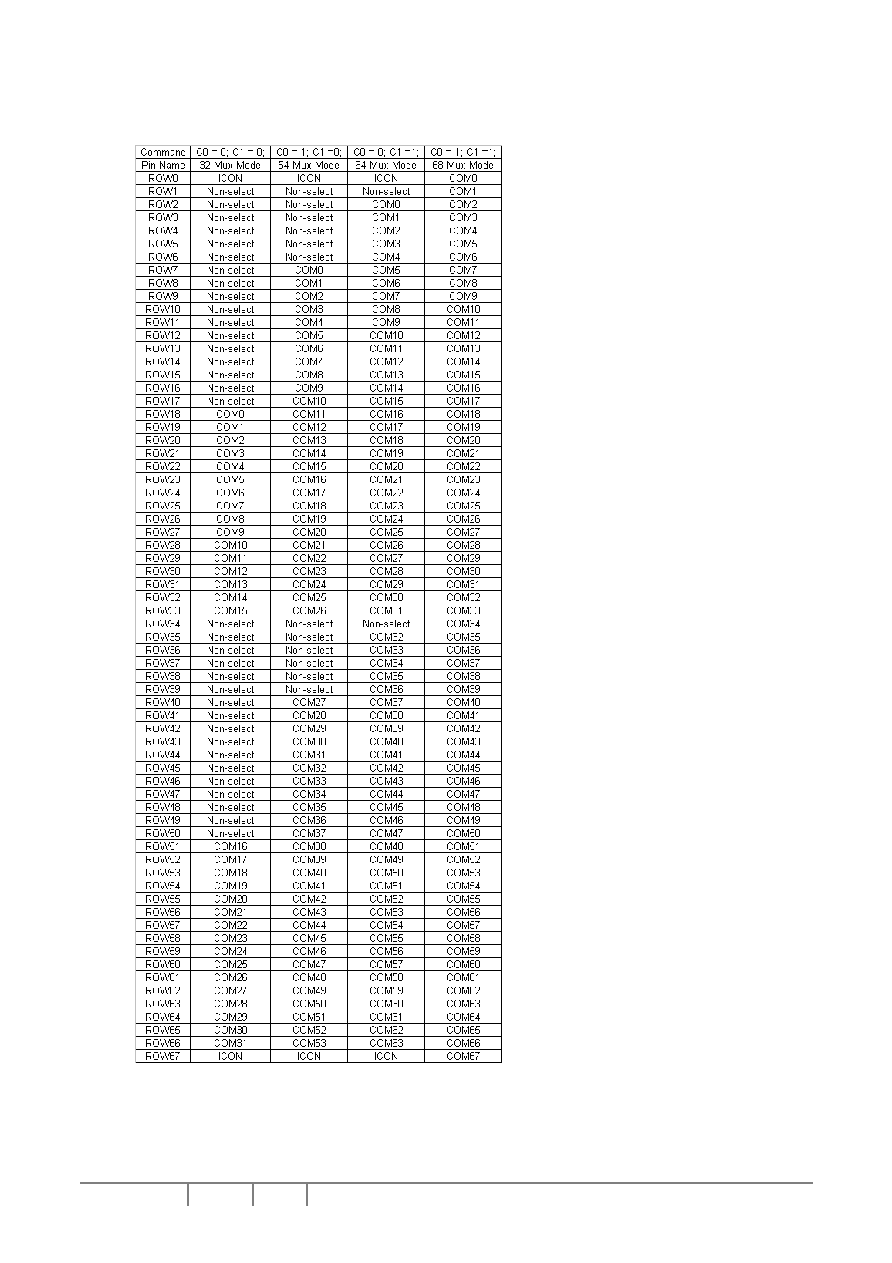
Table 3 - Arrangement of common at different multiplex modes
Remarks: "Non-select" means no common signal will be selected to support those output ROW pins.

Solomon Systech
Jun 2004 P 16/52
Rev 1.1
SSD1805 Series
7 FUNCTIONAL BLOCK DESCRIPTIONS
7.1 Microprocessor Interface Logic
The Microprocessor Interface unit consists of three functional blocks for driving the 6800-series parallel
interface, 8080-series parallel interface and 4-wires serial peripheral interface. The selection of different
interfaces is done by P/
S pin and C68/ 80 pin. Please refer to the pin descriptions on page 8.
a) MPU 6800-series Parallel Interface
The parallel interface consists of 8 bi-directional data pins (D7-D0), R/
W
(
WR
), D/
C
, E(
RD
),
CS
1 and CS2. R/
W
(
WR
) input high indicates a read operation from the Graphic Display Data
RAM (GDDRAM) or the status register. R/
W
(
WR
) input Low indicates a write operation to
Display Data RAM or Internal Command Registers depending on the status of D/
C
input. The
E(
RD
) input serves as data latch signal (clock) when high provided that
CS
1 and CS2 are low
and high respectively. Please refer to Figure 11 & 12 on page 40 & 41 for Parallel Interface
Timing Diagram of 6800-series microprocessors. In order to match the operating frequency of the
GDDRAM with that of the MCU, some pipeline processing is internally performed which requires
the insertion of a dummy read before the first actual display data read. This is shown in Figure 3.
Figure 3 - Display Data Read with the insertion of dummy read
b) MPU 8080-series Parallel Interface
The parallel interface consists of 8 bi-directional data pins (D7-D0), E(
RD
), R/
W
(
WR
), D/
C
,
CS
1 and CS2. E(
RD
) input serves as data read latch signal (clock) when low provided that
CS
1
and CS2 are low and high respectively. Whether reading the display data from GDDRAM or
reading the status from status register is controlled by D/
C
. R/
W
(
WR
) input serves as data write
latch signal (clock) when low provided that
CS
1 and CS2 are low and high respectively. Whether
writing the display data to the GDDRAM or writing the command to the command register is
controlled by D/
C
. A dummy read is also required before the first actual display data read for
8080-series interface. Please refer to figure 13 & 14 on page 42 & 43 for Parallel Interface Timing
Diagram of 8080-series microprocessors.
c) MPU 4-wires Serial Interface
The 4-wires serial interface consists of serial clock SCK (D6), serial data SDA (D7), D/
C
,
CS
1
and CS2. SDA is shifted into a 8-bit shift register on every rising edge of SCK in the order of data
bit 7, data bit 6, ..., data bit 0. D/
C
is sampled on every eighth clock to determine whether the
data byte in the shift register is written to the Display Data RAM or command register at the same
clock. Please refer to figure 15 & 16 on page 43 & 44 for serial interface timing.
Remarks: For SPI mode, it is necessary to add one time of software reset command (code: E2) in
the first line of the initialization code.
R/W(WR)
E (RD)
N
n
n+1
n+2
data bus
write column address
dummy read
data read1
data read 2
data read 3

SSD1805 Series
Rev 1.1
P 17/52
Jun 2004
Solomon Systech
Table 4 - Data Bus selection Modes
7.2 Reset
Circuit
This block is integrated into the Microprocessor Interface Logic that includes Power On Reset circuitry and the
hardware reset pin,
RES
. Both of these having the same reset function. Once
RES
receives a negative reset
pulse, all internal circuitry will start to initialize. Minimum pulse width for completing the reset sequence is
20us. Status of the chip after reset is given by:
When
RES
input is low, the chip is initialized to the following:
1) Display ON/OFF:
Display is turned OFF
2)
Normal/Inverse
Display:
Normal
Display
3) Com Scan Direction:
COM0 -> COM67
4)
Internal
Oscillator:
Enable
5) Internal DC-DC Converter:
Disable
6)
Bias
Divider: Disable
7) Booster level:
Determine by pins [B0, B1]
8) Bias ratio:
1/8 for 32 & 54 Mux mode
1/9 for 64 & 68 Mux mode
9) Multiplex ratio:
Determine by pins [C0, C1]
10) Electronic volume control:
20 hex
11) Built-in resistance ratio:
24 hex
12) Average temperature gradient:
-0.05%/
o
C
13) Display data column address mapping:
Normal
14) Display start line:
GDDRAM row 0
15) Column address counter:
00 hex
16)
Page
address:
00
hex
17)
Static
indicator:
Disable
18)
Read-modify-write
mode:
Disable
19)
Test
mode:
Disable
20) Shift register data in serial interface:
Clear
Note: Please find more explanation in the Applications Note attached at the back of the specification.
7.3 Command Decoder and Command Interface
This module determines whether the input data is interpreted as data or command. Data is directed to this
module based upon the input of the D/
C
pin. If D/
C
pin is high, data is written to Graphic Display Data RAM
(GDDRAM). If D/
C
pin is low, the input at D0 � D7 is interpreted as a Command and it will be decoded. The
decoded command will be written to the corresponding command register.
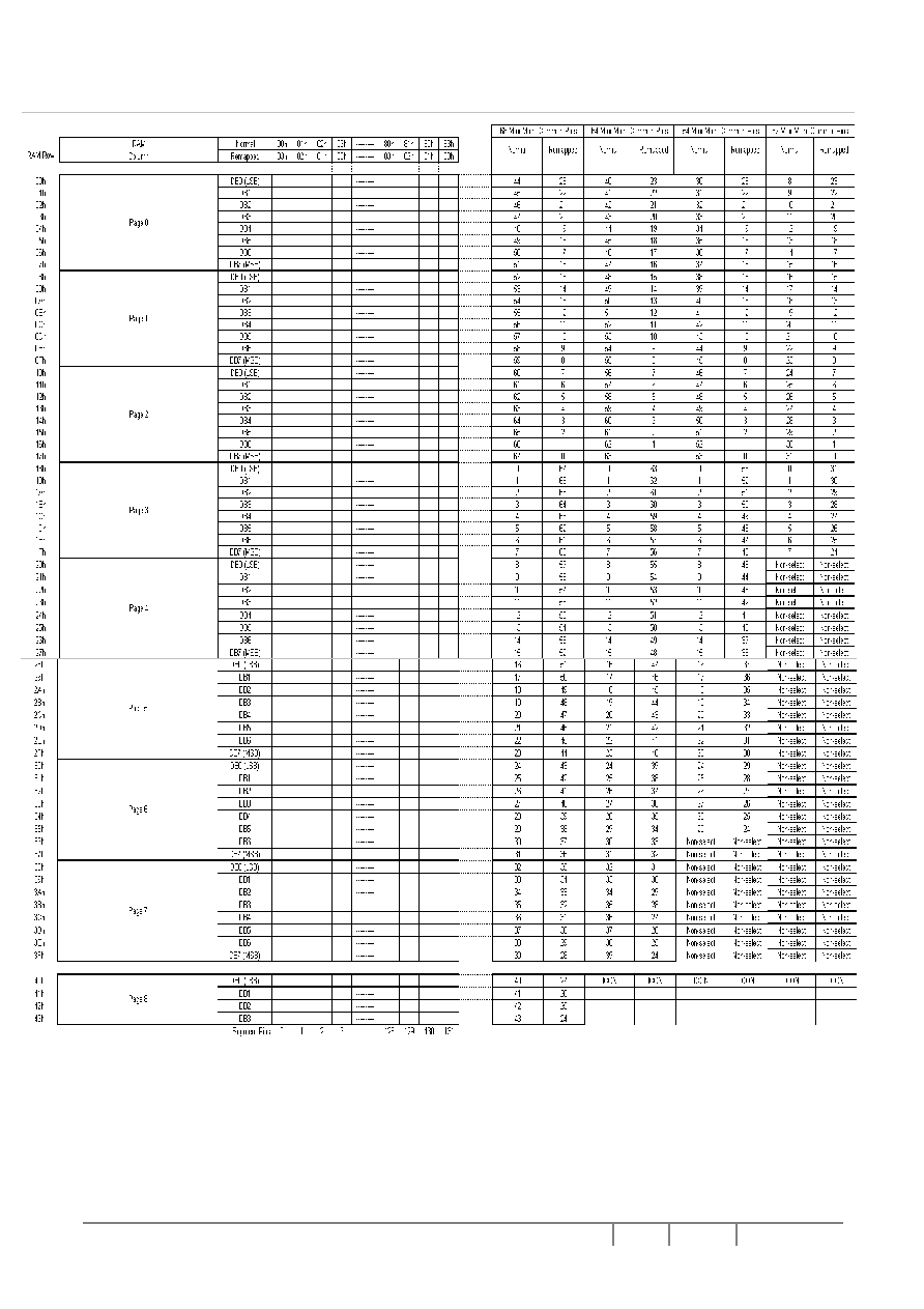
7.4 Graphic Display Data RAM (GDDRAM)
The GDDRAM is a bit mapped static RAM holding the bit pattern to be displayed. The size of the RAM is 132
x 68 = 8,976bits. Table 5 on page 18 is a description of the GDDRAM address map in which the display start
line register is set at 18H. For mechanical flexibility, re-mapping on both Segment and Common outputs are
provided. For vertical scrolling of display, an internal register storing the display start line can be set to control
the portion of the RAM data mapped to the display. For those GDDRAM out of the display common range,
they could still be accessed, for either preparation of vertical scrolling data or even for the system usage.
Please be noticed that the display offset cannot be greater than the default mux mode for any circumstance.
6800-series Parallel Interface 8080-series Parallel Interface 4-wires Serial Peripheral Interface
Data
Read
8-bits 8-bits No
Data
Write
8-bits 8-bits 8-bits
Command Read Status only
Status only
No
Command
Write
Yes Yes Yes
Solomon Systech
Jun 2004 P 18/52
Rev 1.1
SSD1805 Series
Remarks:
DB0 � DB7 represent the data bit of the GDDRAM.
"Non-select" means no common signal will be selected to support those output ROW pins.
Table 5 - Graphic Display Data RAM (GDDRAM) Address Map with Display Start Line set to 18h
SSD1805 Series
Rev 1.1
P 19/52
Jun 2004
Solomon Systech
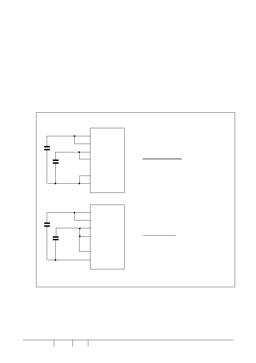
7.5 LCD Driving Voltage Generator and Regulator
This module generates the LCD voltage required for display driving output. It takes a single supply input and
generates necessary bias voltage. It consists of:
1) 2X, 3X, 4X and 5X regulated DC-DC voltage converter
The built-in DC-DC regulated voltage converter is used to generate the large positive voltage supply.
SSD1805 can produce 2X, 3X, 4X or 5X boosting from the potential different between V
SS1
- V
CI
. No
external boosting capacitors are required for configuration. Please refer to the command table for detail
description. The feedback gain control for LCD driving contrast curves can be selected by IRS pin to
either internal (IRS pin = H) or external (IRS pin = L). If internal resistor network is enabled, eight settings
can be selected through software command. If external control is selected, external resistors are required
to connect between V
ss
and V
F
(R1), and between V
F
and V
OUT
(R2). See application circuit diagrams for
detail connections.
Figure 4 - SSD1805 Hardware configuration
2) Bias
Divider
If the output op-amp buffer option in Set Power Control Register command is enabled, this circuit block
will divide the regulator output (V
OUT
) to give the LCD driving levels. The divider does not require external
capacitors to reduce the external hardware and pin counts.
3) Bias Ratio Selection circuitry
The software control circuit of 1/4 to 1/9 bias ratio in order to match the characteristic of LCD panel.
V
OUT
V
HREF
V
DD
V
CI
V
LREF
V
SS
+
+
SSD1805
Normal Power Mode
Recommended capacitance value:
C
1
: 1uF ~ 2.2uF
C
2
: 2.2uF ~ 4.7uF
C
1
C
2
V
OUT
V
HREF
V
DD
V
CI
V
LREF
V
SS
+
+
SSD1805
Low Power Mode
In Low Power Mode, TEST4 must > 4V
Recommended capacitance value:
C
1
: 1uF ~ 2.2uF
C
2
: 2.2uF ~ 4.7uF
C
1
C
2
Solomon Systech
Jun 2004 P 20/52
Rev 1.1
SSD1805 Series
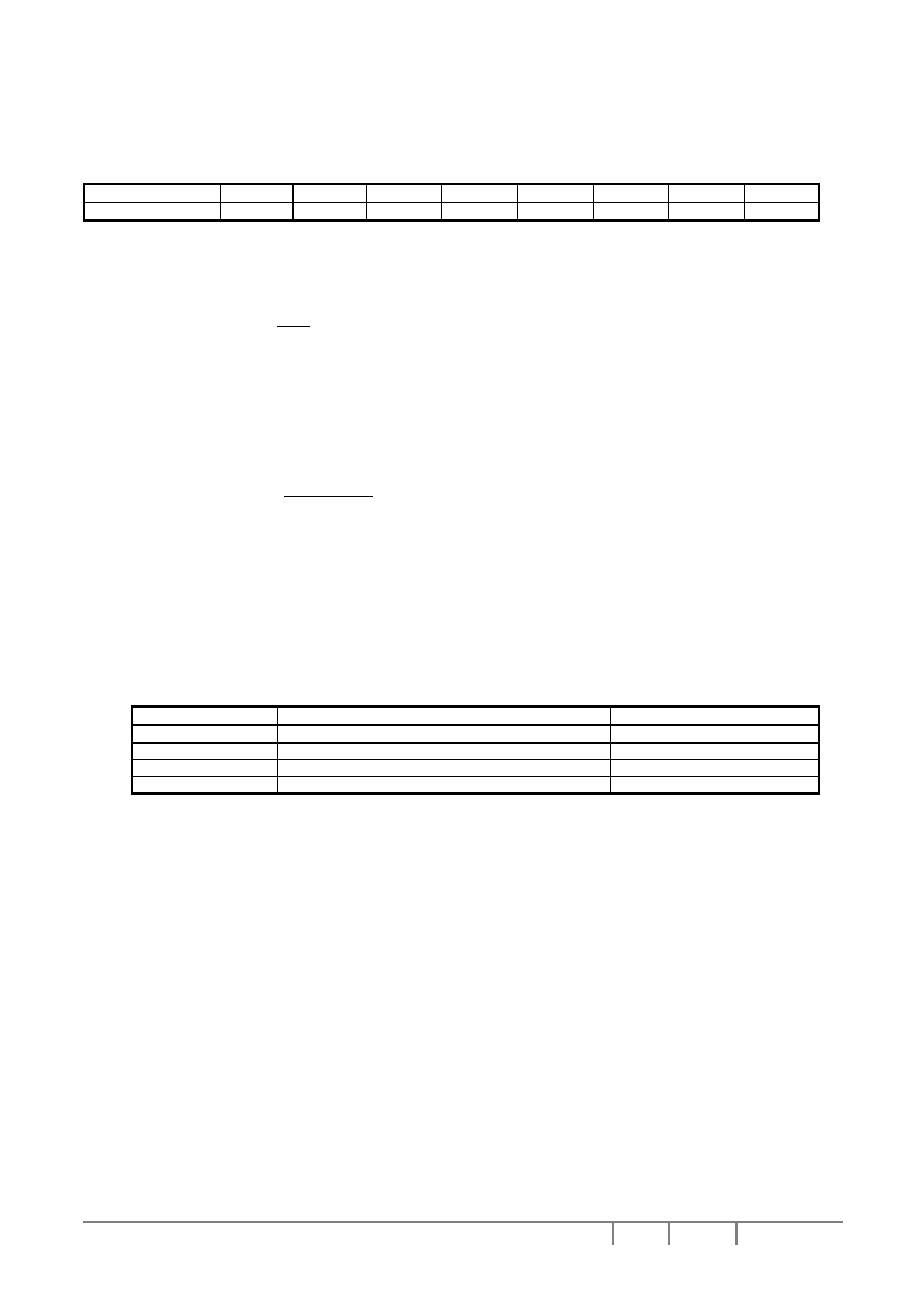
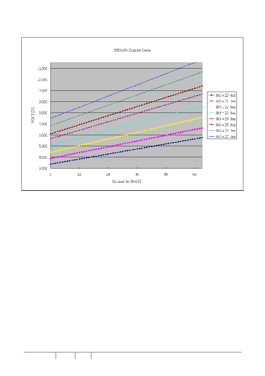
4) Contrast Control (Voltages referenced to V
SS
)
Software control of the 64 contrast voltage levels at each voltage regulator feedback gain. The equation
of calculating the LCD driving voltage is given as:
Command
Set
000 001 010 011 100 101 110 111
Gain = 1+R
2
/R
1
4.96 5.70 6.54 7.41 8.33 8.95 10.05 11.01
Table 6 - Gain Setting
where V
ref
=
1.6 and
= contrast setting
Please refer to figure 5 on page 21 for the contrast curve with 8 sets of internal resistor network gain.
5) Self adjust temperature compensation circuitry
Provide 4 different compensation grade selections to satisfy the various liquid crystal temperature grades.
The grading can be selected by software control. Defaulted temperature coefficient (TC) value is �0.05%/�C.
TC Settings
Temperature compensation coefficient [%/
o
C]
Vref typical value [V]
TC0 -0.05
1.60
TC2 -0.15
1.70
TC4 -0.20
1.75
TC7 -0.25
1.85
Table 7 - Temperature compensation coefficient
con
out
V
R
R
V
*
1
1
2
+
=
ref
con
V
V
*
210
121
1
-
-
=
SSD1805 Series
Rev 1.1
P 21/52
Jun 2004
Solomon Systech
Figure 5 - Contrast curve
Solomon Systech
Jun 2004 P 22/52
Rev 1.1
SSD1805 Series
7.6 Oscillator
Circuit
This module is an On-Chip low power temperature compensation oscillator circuitry. The oscillator generates
the clock for the DC-DC voltage converter. This clock is also used in the Display Timing Generator. Please
refer to the figure 6 for the typical frame frequency at different temperature.
Figure 6 - Oscillator typical frame frequency with variation in temperature
7.7 Display Data Latch
This block is a series of latches carrying the display signal information. These latches hold the data, which will
be fed to the HV Buffer Cell and Level Selector to output the required voltage level.
The numbers of latches of
different members are given by:
32 Mux mode: 132 + 33 = 165
54 Mux mode: 132 + 55 = 187
64 Mux mode: 132 + 65 = 197
68 Mux mode: 132 + 68 = 200
7.8 HV Buffer Cell (Level Shifter)
This block is embedded in the Segment/Common Driver Circuits. HV Buffer Cell works as a level shifter,
which translates the low voltage output signal to the required driving voltage. The output is shifted out with an
internal FRM clock, which comes from the Display Timing Generator. The voltage levels are given by the level
selector that is synchronized with the internal M signal.
7.9 Level
Selector
This block is embedded in the Segment/Common Driver Circuits. Level Selector is a control of the display
synchronization. Display voltage levels can be separated into two sets and used with different cycles.
Synchronization is important since it selects the required LCD voltage level to the HV Buffer Cell, which in
turn outputs the COM or SEG LCD waveform.
SSD1805 Series
Rev 1.1
P 23/52
Jun 2004
Solomon Systech
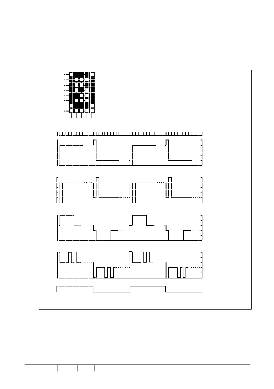
7.10 LCD Panel Driving Waveform
Figure 7 is an example of how the Common and Segment drivers may be connected to a LCD panel. The
waveforms provided illustrate the desired multiplex scheme.
Figure 7 - LCD Driving Waveform
TIME SLOT
COM0
COM1
SEG0
SEG1
M
* Note : N is the number of multiplex ratio including Icon line if it is enabled, N is equal to 64 on POR .
V
o ut
V
L5
V
L4
V
L3
V
L2
V
S S
V
o ut
V
L5
V
L4
V
L3
V
L2
V
S S
V
o ut
V
L5
V
L4
V
L3
V
L2
V
S S
V
o ut
V
L5
V
L4
V
L3
V
L2
V
S S
1 2 3 4 5 6 7 8 9
. . .
N
*
1 2 3 4 5 6 7 8 9
. . .
N
*
1 2 3 4 5 6 7 8 9
. . .
N
*
1 2 3 4 5 6 7 8 9
. . .
N
*
COM1
COM2
COM3
COM4
COM5
COM6
COM7
SEG
1
SEG
2
SEG
3
SEG
4
COM0
SEG
0
*Note: N is the number of multiplex ratio including Icon line if it is enabled; N is equal to 68 on POR.
Solomon Systech
Jun 2004 P 24/52
Rev 1.1
SSD1805 Series
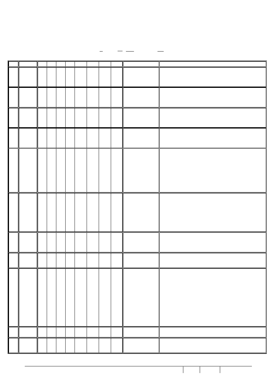
8 COMMAND TABLE
Table 8 - Command Table (D/ C = 0, R/
W
( WR ) = 0, E=1( RD = 1) unless specific setting is stated)
D/C Hex D7 D6 D5 D4 D3 D2 D1 D0
Command
Description
0
0 0 0 0 X
3
X
2
X
1
X
0
00 � 0F
Set Lower
Column Address
Set the lower nibble of the column address register
using X
3
X
2
X
1
X
0
as data bits. The lower nibble of column
address is reset to 0000b after POR.
0
0 0 0 1 X
3
X
2
X
1
X
0
10 � 1F
Set Higher
Column Address
Set the higher nibble of the column address register
using X
3
X
2
X
1
X
0
as data bits. The higher nibble of
column address is reset to 0000b after POR.
0
20 � 27
0 0 1 0 0 X
2
X
1
X
0
Set Internal Gain
Resistor Ratio
Feedback gain of the internal regulated DC-DC
converter for generating VOUT increases as X
2
X
1
X
0
increased from 000b to 111b. After POR, X
2
X
1
X
0
=
100b.
0
28 � 2F
0
0
1
0
1
X
2
1 X
0
Set
Power
Control Register
X
0
=0: turns off the output op-amp buffer (POR)
X
0
=1: turns on the output op-amp buffer
X
2
=0: turns off the internal voltage booster (POR)
X
2
=1: turns on the internal voltage booster
0 1 X
5
X
4
X
3
X
2
X
1
X
0
* Y
6
Y
5
Y
4
Y
3
Y
2
Y
1
Y
0
0
0
40 � 7F
Set Display Start
Line
For 68 MUX mode, set X
5
X
4
X
3
X
2
X
1
X
0
= 111111 and set
the GDDRAM display start line register from 0-67 using
Y
6
Y
5
Y
4
Y
3
Y
2
Y
1
Y
0
For 64/54/32 MUX modes, set GDDRAM display start
line register from 0-63 using X
5
X
4
X
3
X
2
X
1
X
0.
There is no need to send the Y
6
Y
5
Y
4
Y
3
Y
2
Y
1
Y
0
parameters.
Display start line register is reset to 000000 after POR
for all MUX modes.
0
84 � 87
1
0
0
0
0
1
X
1
X
0
Set Boost Level
Set the DC-DC multiplying factor from 2X to 5X.
X
1
X
0
:
00: 3X
01: 4X
10: 5X
11: 2X
Remarks: The POR default boosting level is determined
by hardware selection pin, B0 & B1.
1 0 0 0 0 0 0 1
0 0 X
5
X
4
X
3
X
2
X
1
X
0
0
0
81
Set Contrast
Control Register
Select contrast level from 64 contrast steps. Contrast
increases (VOUT decreases) as X
5
X
4
X
3
X
2
X
1
X
0
is
increased from 000000b to 111111b. X
5
X
4
X
3
X
2
X
1
X
0
=
100000b after POR
0
A0 � A1 1
0
1
0
0
0
0
X
0
Set Segment Re-
map
X
0
=0: column address 00h is mapped to SEG0 (POR)
X
0
=1: column address 83h is mapped to SEG0
Refer to Table 5 on page 16 for example.
0
A2 � A3 1
0
1
0
0
0
1
X
0
Set LCD Bias
X
0
=0: POR default bias:
32 MUX mode = 1/8
54 MUX mode = 1/8
64 MUX mode = 1/9
68 MUX mode = 1/9
X
0
=1: alternate bias:
32 MUX mode = 1/6
54 MUX mode = 1/6
64 MUX mode = 1/7
68 MUX mode = 1/7
For other bias ratio settings, see "Set 1/4 Bias Ratio"
and "Set Bias Ratio" in Extended Command Set.
0
A4 � A5 1
0
1
0
0
1
0
X
0
Set
Entire
Display On/Off
X
0
=0: normal display (POR)
X
0
=1: entire display on
0
A6 � A7 1
0
1
0
0
1
1
X
0
Set
Normal/Reverse
Display
X
0
=0: normal display (POR)
X
0
=1: reverse display
SSD1805 Series
Rev 1.1
P 25/52
Jun 2004
Solomon Systech
D/C Hex D7
D6
D5
D4 D3 D2 D1 D0 Command
Description
0 AE � AF 1
0
1
0
1
1
1
X
0
Set
Display
On/Off
X
0
=0: turns off LCD panel (POR)
X
0
=1: turns on LCD panel
0
B0 � B8 1
0
1
1
X
3
X
2
X
1
X
0
Set
Page
Address
Set GDDRAM Page Address (0-8) for read/write using
X
3
X
2
X
1
X
0
0 C0 � C8 1
1
0
0
X
3
*
*
*
Set COM Output
Scan Direction
X
3
=0: normal mode (POR)
X
3
=1: remapped mode,
COM0 to COM [N-1] becomes COM [N-1] to COM0
when Multiplex ratio is equal to N.
See Table 5 on page 16 for detail mapping.
0 E0 1 1 1 0 0 0 0 0 Set
Read-Modify-
Write Mode
Read-Modify-Write mode will be entered in which the
column address will not be increased during display
data read. After POR, Read-modify-write mode is
turned OFF.
0
E2
1
1
1
0
0
0
1
0
Software Reset
Initialize internal status registers.
0 EE 1 1 1 0 1 1 1 0 Set
End
of
Read-
Modify-Write
Mode
Exit Read-Modify-Write mode. RAM Column address
before entering the mode will be restored. After POR,
Read-modify-write mode is OFF.
1 0 1 0 1 1 0 X
0
* * * * * * Y
1
Y
0
0
0
AC � AD
Indicator Display
Mode
X
0
= 0: indicator off (POR, second command byte is not
required)
X
0
= 1: indicator on (second command byte required)
Y
1
Y
0
= 00: indicator off
Y
1
Y
0
= 01: indicator on and blinking at ~1 second
interval
Y
1
Y
0
= 10: indicator on and blinking at ~1/2 second
interval
Y
1
Y
0
= 11: indicator on constantly
This second byte command is required ONLY when
"Set Indicator On" command is sent.
0
E3
1
1
1
0
0
0
1
1
NOP
Command result in No Operation.
0
F0 � FF 1
1
1
1
*
*
*
*
Set Test Mode
Reserved for IC testing. Do NOT use.
AE 1
0
1
0 1 1 1 0
A5 1
0
1
0 0 1 0 1
1 0 1 0 1 1 0 X
0
0
0
0
0
* * * * * * X
1
X
0
Set Power Save
Mode
Either standby or sleep mode will be entered using
compound commands.
Issue compound commands "Set Display Off" followed
by "Set Entire Display On". Standby mode will be
entered when the static indicator is on constantly. Sleep
mode will be entered when static indicator is off.
Solomon Systech
Jun 2004 P 26/52
Rev 1.1
SSD1805 Series
EXTENDED COMMAND TABLE
Table 9 - Extended Command Table(D/ C = 0,R/
W
( WR ) = 0,E=1( RD = 1) unless specific setting is stated)
D/C Hex D7
D6
D5
D4 D3 D2 D1 D0 Command
Description
0 1
0
0
0
0
0
1
0
0 *
0
0
0
X
3
X
2
X
1
X
0
82
OTP Setting
X
3
X
2
X
1
X
0
: OTP fuse value
0000 : original contrast
0001 : original contrast + 1 steps
0010 : original contrast + 2 steps
0011 : original contrast + 3 steps
0100 : original contrast + 4 steps
0101 : original contrast + 5 steps
0110 : original contrast + 6 steps
0111 : original contrast + 7 steps
1000 : original contrast - 8 steps
1001 : original contrast - 7 steps
1010 : original contrast - 6 steps
1011 : original contrast - 5 steps
1100 : original contrast - 4 steps
1101 : original contrast - 3 steps
1110 : original contrast - 2 steps
1111 : original contrast - 1 steps
0 83 1 0 0 0 0 0 1 1 OTP
Programming
This command starts to program LCD driver with OTP
offset value. Each bit can be programmed to 1 once.
Detail of OTP programming procedure on page 31
1 0 1 0 1 0 0 0
0 X
6
X
5
X
4
X
3
X
2
X
1
X
0
0
0
A8
Set Multiplex
Ratio
To select multiplex ratio N from 2 to the maximum
multiplex ratio (POR value) for each member (including
icon line for 65 MUX mode).
Max. MUX ratio:
68 MUX: 68
N = X
6
X
5
X
4
X
3
X
2
X
1
X
0
+ 1 + ICON*, (*ICON exist for
64/54/32 MUX mode)
e.g. N = 001111b + 2 = 17
1 0 1 0 1 0 0 1
X
7
X
6
X
5
X
4
X
3
X
2
X
1
X
0
0
0
A9
Set Bias Ratio
Set TC Value
Modify Osc.
Freq.
MUX X
1
X
0
= 00 01 10 11
32 : 1/8 or 1/6(POR) 1/6 or 1/5 1/9 or 1/7 P
54 : 1/8 or 1/6(POR) 1/6 or 1/5 1/9 or 1/7 P
64 : 1/8 or 1/6 1/6 or 1/5 1/9 or 1/7(POR) P
68 : 1/8 or 1/6 1/6 or 1/5 1/9 or 1/7(POR) P
P stands for prohibited settings
X
4
X
3
X
2
= 000: (TC0) Typ. �0.05 (POR)
X
4
X
3
X
2
= 010: (TC2) Typ. �0.15
X
4
X
3
X
2
= 100: (TC4) Typ. �0.20
X
4
X
3
X
2
= 111: (TC7) Typ. �0.25
Increase the value of X
7
X
6
X
5
will increase the oscillator
frequency and vice versa.
Default Mode:
X
7
X
6
X
5
Osc Frequency (Hz)
000 61
001 64
010 68
011 72 (POR)
100 75
101 80
110 90
111 98
Remarks: By software program the multiplex ratio, the
typical oscillator frequency is listed above.
0 AA � AB 1
0
1
0
1
0
1
X
0
Set � Bias Ratio
X
0
= 0: use normal setting (POR)
X
0
= 1: fixed at 1/4 bias regardless of other bias setting
commands

SSD1805 Series
Rev 1.1
P 27/52
Jun 2004
Solomon Systech
D/C Hex D7
D6
D5
D4 D3 D2 D1 D0 Command
Description
0 D0 � D1 1
1
0
1
0
0
0
X
0
Set icon enabled X
0
= 0: icon is off.
X
0
= 1: icon is on. (POR)
1 1 0 1 0 0 1 1
0
0
D3
0 X
6
X
5
X
4
X
3
X
2
X
1
X
0
Set Display
Offset
Set Total Frame
Phases
After POR, X
6
X
5
X
4
X
3
X
2
X
1
X
0
= 0
After setting MUX ratio less than default value, data will
be displayed at the beginning/towards the end of
display matrix.
To move display towards Row 0 by L, X
6
X
5
X
4
X
3
X
2
X
1
X
0
= L
To move display away from Row 0 by L,
X
6
X
5
X
4
X
3
X
2
X
1
X
0
= Y-L
Note: max. value of L = POR default MUX ratio �
display MUX
Note: Y represents POR default MUX ratio
The On/Off of the Static Icon is given by 3 phases / 1
phase overlapping of the M and MSTAT signals. This
command set total phases of the M/MSTAT signals for
each frame.
The more the total phases, the less the overlapping
time and thus the lower the effective driving voltage.
X
5
X
4
= 00: 5 phases
X
5
X
4
= 01: 7 phases
X
5
X
4
= 10: 9 phases (POR)
X
5
X
4
= 11: 16 phases
1 1 0 1 0 1 0 0
0
0
D4
0 0 X
5
X
4
0 0 0 0
Set Display
Offset
After POR, X
6
X
5
X
4
X
3
X
2
X
1
X
0
= 0
After setting MUX ratio less than default value, data will
be displayed at the beginning/towards the end of
display matrix.
To move display towards Row 0 by L, X
6
X
5
X
4
X
3
X
2
X
1
X
0
= L
To move display away from Row 0 by L,
X
6
X
5
X
4
X
3
X
2
X
1
X
0
= Y-L
Note: max. value of L = POR default MUX ratio �
display MUX
Note: Y represents POR default MUX ratio
READ COMMAND TABLE
Table 10 - Read Command Table (D/ C = 1, R/
W
( WR ) = 1, E=1( RD = 0) unless specific setting is stated)
D/C Hex D7
D6
D5
D4 D3 D2 D1 D0 Command
Description
1
00 - FF X
7
X
6
X
5
0 X
3
X
2
X
1
X
0
Status
Register
Read
X
7
=0: indicates the driver is ready for command.
X
7
=1: indicates the driver is Busy.
X
6
=0: indicates normal segment mapping with
column address.
X
6
=1: indicates reverse segment mapping with
column address.
X
5
=0: indicates the display is ON.
X
5
=1: indicates the display is OFF.
X
3
X
2
X
1
X
0
= 0010, the 4-bit is fixed to 0010 which could
be used to identify as Solomon Systech Device.
Note: Command patterns other than that given in Command Table and Extended Command Table are
prohibited. Otherwise, unexpected result will occur.
Solomon Systech
Jun 2004 P 28/52
Rev 1.1
SSD1805 Series
9 COMMAND DESCRIPTIONS
9.1 Data Read / Write
To read data from the GDDRAM, input High to
R/W ( WR )
pin and
D/ C
pin for 6800-series parallel mode,
input Low to
E( RD )
pin and High to
D/ C
pin for 8080-series parallel mode. No data read is provided in serial
interface mode. In normal data read mode, GDDRAM column address pointer will be increased by one
automatically after each data read. However, no automatic increase will be performed in read-modify-write
mode. Also, a dummy read is required before first valid data is read. See Figure 3 on page 15 in Functional
Block Descriptions section for detail waveform diagram. To write data to the GDDRAM, input Low to
R/W ( WR )
pin and High to
D/ C
pin for both 6800-series and 8080-series parallel mode. For serial interface
mode, it is always in write mode. GDDRAM column address pointer will be increased by one automatically
after each data write. It should be noted that, after the automatic column address increment, the pointer will
NOT wrap round to 0. The pointer will exit the memory address space after accessing the last column.
Therefore, the pointer should be re-initialized when progress to another page address.
D/ C
R/W ( WR )
Action
Auto Address Increment
0 0
Write
Command
No
0 1
Read
Status
No
1 0
Write
Data
Yes
1 1
Read
Data
Yes
Table 11 - Automatic Address Increment
9.2 Set Lower Column Address
This command specifies the lower nibble of the 8-bit column address of the display data RAM. The column
address will be increased by each data access after it is pre-set by the MCU.
9.3 Set Higher Column Address
This command specifies the higher nibble of the 8-bit column address of the display data RAM. The column
address will be increased by each data access after it is pre-set by the MCU.
9.4 Set Internal Gain Resistors Ratio
This command is to enable any one of the eight internal resistor sets for different gains when using internal
resistor network (IRS pin pulled high). In other words, this command is used to select which contrast curve
from the eight possible selections. Please refer to Functional Block Descriptions section for detail calculation
of the LCD driving voltage.
9.5 Set Power Control Register
This command turns on/off the various power circuits associated with the chip. There are two related power
sub-circuits could be turned on/off by this command. Internal voltage booster is used to generate the positive
voltage supply (V
OUT
) from the voltage input (V
CI
- V
SS1
). An external positive power supply is required if this
option is turned off. Output op-amp buffer is the internal divider for dividing the different voltage levels from
the internal voltage booster, V
OUT
. External voltage sources should be fed into this driver if this circuit is turned
off.
9.6 Set Display Start Line
This command is to set Display Start Line register to determine starting address of display RAM to be
displayed by selecting a value from 0 to 67. With value equals to 0, D0 of Page 0 is mapped to COM0. With
value equals to 1, D1 of Page0 is mapped to COM0 and so on. Display start line values of 0 to 67 are
assigned to Page 0 to 8. Please refer to Table 5 on Page 17 as an example for display start line set to 24
(18h).
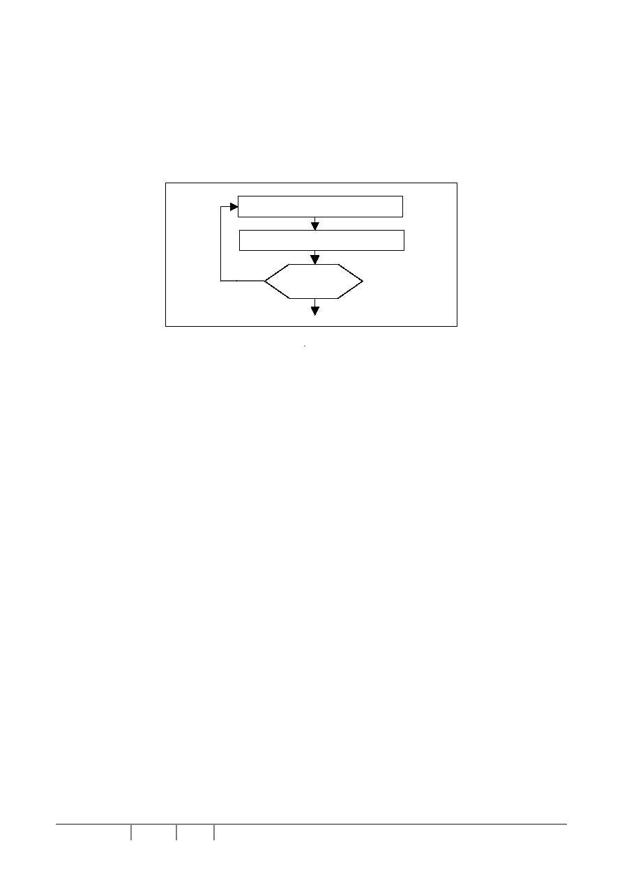
SSD1805 Series
Rev 1.1
P 29/52
Jun 2004
Solomon Systech
9.7 Set Boost level
The internal DC-DC converter factor is set by this command. For SSD1805, 2X to 5X multiplying factors could
be selected. The default POR internal DC-DC converter setting can be selected by hardware pin, B0 & B1.
9.8 Set Contrast Control Register
This command adjusts the contrast of the LCD panel by changing the LCD driving voltage, V
OUT
, provided by
the On-Chip power circuits. V
OUT
is set with 64 steps (6-bit) in the contrast control register by a set of
compound commands. See Figure 8 for the contrast control flow.
Figure 8 - Contrast Control Flow
9.9 Set Segment Re-map
This command changes the mapping between the display data column addresses and segment drivers. It
allows flexibility in mechanical layout of LCD glass design. Please refer to Table 5 on Page 15 for example.
9.10 Set LCD Bias
This command is used to select a suitable bias ratio required for driving the particular LCD panel in use. The
selectable values of this command for 68/64 MUX are 1/9 or 1/7, 54/32 MUX are 1/8 or 1/6. For other bias
ratio settings, extended commands should be used.
9.11 Set Entire Display On/Off
This command forces the entire display, including the icon row, to be illuminated regardless of the contents of
the GDDRAM. In addition, this command has higher priority than the normal/reverse display. This command
is used together with "Set Display ON/OFF" command to form a compound command for entering power save
mode. See "Set Power Save Mode" later in this section.
9.12 Set Normal/Reverse Display
This command turns the display to be either normal or reverse. In normal display, a RAM data of 1 indicates
an illumination on the corresponding pixel. While in reverse display, a RAM data of 0 will turn on the pixel.
It
should be noted that the icon line will not affect, that is not reverse by this command.
9.13 Set Display On/Off
This command is used to turn the display on or off. When display off is issued with entire display is on, power
save mode will be entered. See "Set Power Save Mode" later in this section for details.
9.14 Set Page Address
This command enters the page address from 0 to 8 to the RAM page register for read/write operations.
Please refer to Table 5 on Page 17 for detail mapping.
9.15 Set COM Output Scan Direction
This command sets the scan direction of the COM output allowing layout flexibility in LCD module assembly.
See Table 5 on Page 17 for the relationship between turning on or off of this feature. In addition, the display
will have immediate effect once this command is issued. That is, if this command is sent during normal
display, the graphic display will have vertical flipping effect.
No
Yes
Changes
Complete?
Set Contrast Control Register
Contrast Level Data

Solomon Systech
Jun 2004 P 30/52
Rev 1.1
SSD1805 Series
9.16 Set Read-Modify-Write Mode
This command puts the chip in read-modify-write mode in which:
1. Column address is saved before entering the mode
2. Column address is increased only after display data write but not after display data read.
This Read-Modify-Write mode is used to save the MCU's loading when a very portion of display area is being
updated frequently. As reading the data will not change the column address, it could be get back from the
chip and do some operation in the MCU. Then the updated data could be written back to the GDDRAM with
automatic address increment. After updating the area, "Set End of Read-Modify-Write Mode" is sent to restore
the column address and ready for next update sequence.
9.17 Software Reset
Issuing this command causes some of the chip's internal status registers to be initialized:
Read-Modify-Write mode is off
Static indicator is turned OFF
Display start line register is cleared to 0
Column address counter is cleared to 0
Page address is cleared to 0
Normal scan direction of the COM outputs
Internal gain resistors Ratio is set to 4
Contrast control register is set to 20h
9.18 Set End of Read-Modify-Write Mode
This command relieves the chip from read-modify-write mode. The column address before entering read-
modify-write mode will be restored no matter how much modification during the read-modify-write mode.
9.19 Set Indicator On/Off
This command turns on or off the static indicator driven by the M and MSTAT pins.
When the "Set Indicator On" command is sent, the second command byte "Indicator Display Mode" must be
followed. However, the "Set Indicator Off" command is a single byte command and no second byte command
is required.
The status of static indicator also controls whether standby mode or sleep mode will be entered, after issuing
the power save compound command. See "Set Power Save Mode" later in this section.
9.20 NOP
A command causing the chip takes No Operation.
9.21 Set Test Mode
This command forces the driver chip into its test mode for internal testing of the chip. Under normal operation,
users should NOT use this command.
9.22 Set Power Save Mode
Entering Standby or Sleep Mode should be done by using a compound command composed of "Set Display
ON/OFF" and "Set Entire Display ON/OFF" commands. When "Set Entire Display ON" is issued when display
is OFF, either Standby Mode or Sleep Mode will be entered. The status of the Static Indicator will determine
which power save mode is entered. If static indicator is off, the Sleep Mode will be entered:
Internal oscillator and LCD power supply circuits are stopped
Segment and Common drivers output V
SS
level
The display data and operation mode before sleep are held
Internal display RAM can still be accessed
If the static indicator is on, the chip enters Standby Mode that is similar to sleep mode except addition with:
Internal oscillator is on
Static drive system is on
Please also be noted that during Standby Mode, if the software reset command is issued, Sleep Mode will be
entered. Both power save modes can be exited by the issue of a new software command or by pulling Low at
hardware pin
RES
.

SSD1805 Series
Rev 1.1
P 31/52
Jun 2004
Solomon Systech
EXTENDED COMMANDS
These commands are used, in addition to basic commands, to trigger the enhanced features designed for the
chip.
9.23 OTP setting and programming
OTP (One Time Programming) is a method to adjust V
OUT
. In order to eliminate the variations of LCD module
in term of contrast level, OTP can be used to achieve the best contrast of every LCD modules. OTP setting
and programming should include two major steps. Find the OTP offset and OTP programming as following,
Step 1. Find OTP offset
Hardware Reset (sending an active low reset pulse to
RES pin)
Send original initialization routines
Set and display any test patterns
Adjust the contrast value 0x81, 0x00~0x3Funtil there is the best visual contrast
OTP setting steps = Contrast value of the best visual contrast - Contrast value of original initialization
Example 1
Contrast value of original initialization = 0x20
Contrast value of the best original initialization = 0x24
OTP offset value = 0x24 - 0x20 = +4
OTP setting command should be (0x82, 0x04)
Example 2:
Contrast value of original initialization = 0x20
Contrast value of the best original initialization = 0x1B
OTP setting = 0x1B - 0x20 = -6
OTP setting command should be (0x82, 0x0A)
Step 2. OTP programming
Hardware Reset (sending an active low reset pulse to
RES pin)
Connect an external V
OUT
(see diagram below)
Send OTP setting commands that we find in step 1 (0x82, 0x00~0X0F)
Send OTP programming command (0x83)
Wait at least 2 seconds
Hardware Reset
Verify the result by repeating step 1. (2) � (3)
Figure 9 - OTP programming circuitry
R
+
-
SSD1805
V
OUT
RES
14.5-15.5V
Note: R = 1K ~ 10k ohm
C = 1u ~ 4.7u F
C
(8)
(1) & (6) &
GND
GND
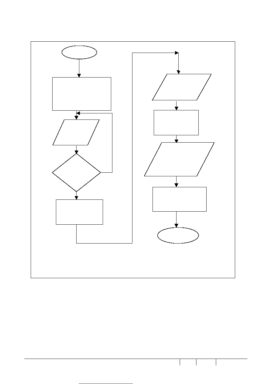
Solomon Systech
Jun 2004 P 32/52
Rev 1.1
SSD1805 Series
Figure 10 - Flow chart of OTP programming Procedure
Start
OTP setting steps =
Adjusted contrast value
� Original contrast value
Connect an external
voltage (14.5~15.5V)
on V
OUT
pins
i) Send original initialization
routines
ii) Set and display any test
patterns
iii) Inspect the contrast
i) Hardware reset
ii) Enable oscillator
END
Yes
No
Adjust the
contrast level
to the best
visual level
Accept the
contrast level
on panel?
i) Send OTP setting
commands
ii) Send OTP programming
command
iii) Wait > 2 sec
iv) Hardware reset
i) Hardware reset
ii) Send original initialization
routines
iii) Set and display any test
patterns
Step 1
Step 2

SSD1805 Series
Rev 1.1
P 33/52
Jun 2004
Solomon Systech
OTP Example program
Find the OTP offset:
Hardware reset by sending an active low reset pulse to
RES
pin
0X2F \\ turn on the internal voltage booster & output op-amp buffer.
0XA2 \\ Set Biasing ratio
0XA9 \\ 1/9 for 68/64 MUX mode
0X62
0X81 \\Set target gain and contrast.
0X20 \\ contrast = 20 Hex.
0X24 \\ IR4 =>
\\ Set target display contents
0x00
\\ set start column address at 0000 binary for lower nibble
0X10 \\ set start column address at 0000 binary for upper nibble
0XB0 \\ set page address at page 0
0xAF \\ display on
OTP offset calculation... target OTP offset value is +6
OTP programming:
Hardware reset by sending an active low reset pulse to
RES
pin
Connect a external V
OUT
(14.5V~15.5V)
0X82 \\ Set OTP offset value to +6 (0110)
0X06 \\ 0000 X
3
X
2
X
1
X
0
, where X
3
X
2
X
1
X
0
is the OTP offset value
0X83 \\ Send the OTP programming command.
Wait at least 2 seconds for programming wait time.
Verify the result:
After OTP programming, procedure 2 to 5 are repeated for inspection of the contrast on the panel.
9.24 Set Multiplex Ratio
This command switches default multiplex ratio to any multiplex mode from 2 to the maximum multiplex ratio
(POR value), including the icon line.
Max. MUX ratio: 68 for 68 MUX mode
65 for 64 MUX mode including icon line
55 for 54 MUX mode including icon line
33 for 32 MUX mode including icon line
The chip pins ROW0 - ROW67 will be switched to corresponding COM signal output, see Table 12 on Page
35 for examples with and without 8 lines display offset for different MUX. It should be noted that after
changing the display multiplex ratio, the bias ratio need to be adjusted to make display contrast consistent.
9.25 Set Bias Ratio
Except the 1/4 bias, all other available bias ratios could be selected using this command plus the "Set LCD
Bias" command. For detail setting values and POR default, please refer to the extended command table,
Table 9 on Page 26.
9.26 Set Temperature Coefficient (TC) Value
One out of 4 different temperature coefficient settings is selected by this command in order to match various
liquid crystal temperature grades. Please refer to the extended command table, Table 9 on Page 26, for
detailed TC values.
9.27 Modify Oscillator Frequency
The oscillator frequency can be fine tuned by applying this command. Since the oscillator frequency will be
affected by some other factors, this command is not recommended for general usage. Please contact
Solomon Systech application engineers for more detail explanation on this command.

Solomon Systech
Jun 2004 P 34/52
Rev 1.1
SSD1805 Series
9.28 Set 1/4 Bias Ratio
This command sets the bias ratio directly to 1/4. This bias ratio is especially designed for use in under 12
MUX display. In order to restore to other bias ratio, this command must be executed, with LSB=0, before the
"Set Multiplex ratio" or "Set LCD Bias" command is sent.
9.29 Set Icon Enabled
This command enables or disables the icon. It should be noticed that the default setting (POR) will enable the
icon.
9.30 Set Display Offset
This command should be sent ONLY when the multiplex ratio is set less than the default value.
When a lesser multiplex ratio is set, the display will be mapped in the top (y-direction) of the LCD, see the no
offset columns on Table 3 on Page 15. Use this command could move the display vertically within the 67
commons. To make the Reduced-MUX Com 0 (Com 0 after reducing the multiplex ratio) towards the Row 0
direction for L lines, the 7-bit data in second command should be given by L. An example for 8 line moving
towards to Com 0 direction is given on Table 12 on Page 35. To move in the other direction by L lines, the 8-
bit data should be given by 67-L. Please note that the display is confined within the default multiplex value.
9.31 Set Total Frame Phases
The total number of phases for one display frame is set by this command. The Static Icon is generated by the
overlapping of M and MSTAT signals. These two pins output either V
SS
or V
DD
at same frequency but with
phase different. To turn on the Static Icon, 3 phases overlapping is applied to these signals, while 1 phase
overlapping is given to the off status. The more the total number of phases in one frame, the less the
overlapping time. Thus the lower the effective driving voltage at the Static Icon on the LCD panel.
9.32 Status register Read
This command is issued by pulling
D/ C
Low during a data read (refer to Figure 11 on Page 40 and Figure 13
on Page 42 for parallel interface waveforms). It allows the MCU to monitor the internal status of the chip. No
status read is provided for serial mode.
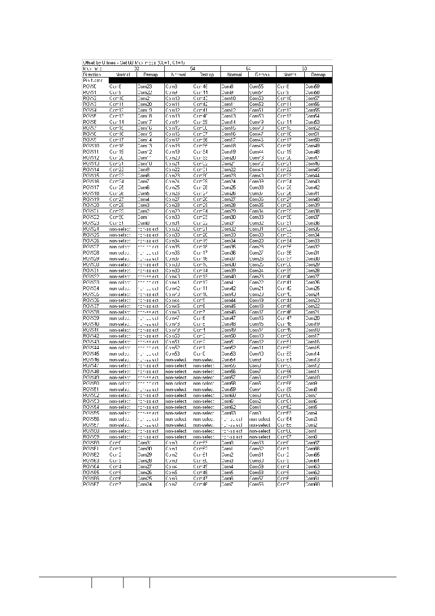
SSD1805 Series
Rev 1.1
P 35/52
Jun 2004
Solomon Systech
Table 12 - ROW pin assignment for COM signals for SSD1805 in a 68 MUX display
(including icon line without/with 8 lines display offset towards ROW0)
Remarks: "Non-select" means no common signal will be selected to support those output ROW pins.
Solomon Systech
Jun 2004 P 36/52
Rev 1.1
SSD1805 Series
10 MAXIMUM RATINGS
Table 13 - Maximum Ratings (Voltage Referenced to V
SS
)
Symbol Parameter
Value
Unit
V
DD
-0.3 to +4.0
V
V
DDIO
-0.3 to + 4.0
V
V
OUT
Supply Voltage
0 to +15.0
V
V
CI
Input Voltage
VSS-0.3 to 4.0
V
I
Current Drain Per Pin Excluding V
DD
and
V
SS
25 mA
T
A
Operating Temperature
-30 to +85
o
C
T
stg
Storage Temperature
-65 to +150
o
C
Ron Input
Resistance
1000
ohm
Maximum ratings are those values beyond which damages to the device may occur. Functional operation should be restricted to the limits in the Electrical
Characteristics tables or Pin Description section.
This device contains circuitry to protect the inputs against damage due to high static voltages or electric fields; however, it is advised that normal
precautions to be taken to avoid application of any voltage higher than maximum rated voltages to this high impedance circuit. For proper operation it is
recommended that V
CI
and V
OUT
be constrained to the range V
SS
< or = (V
CI
or V
OUT
) < or = V
DD
. Reliability of operation is enhanced if unused input is
connected to an appropriate logic voltage level (e.g., either V
SS
or V
DD
). Unused outputs must be left open. This device may be light sensitive. Caution
should be taken to avoid exposure of this device to any light source during normal operation. This device is not radiation protected.
SSD1805 Series
Rev 1.1
P 37/52
Jun 2004
Solomon Systech
11 DC CHARACTERISTICS
Table 14 - DC Characteristics
Symbol Parameter
Test
Condition
Min
Typ
Max
Unit
V
DD
System power supply pins of
the logic block Range
Recommend Operating Voltage
Possible Operating Voltage
1.8 2.7
3.6 V
V
DDIO
System power supply pins of
the logic block Range
Recommend Operating Voltage
Possible Operating Voltage
1.2 -
V
DD
V
V
CI
Booster Reference Supply
Voltage Range
Recommend Operating Voltage
Possible Operating Voltage
V
DD
-
3.6 V
I
AC
Access Mode Supply Current
Drain (V
DD
Pins)
V
DD
= 2.7V, Voltage Generator On,
4X DC-DC Converter Enabled,
Write accessing, Tcyc =3.3MHz,
Typ. Osc. Freq., Display On, no
panel attached.
- 450
750
�A
I
DP1
Display Mode Supply Current
Drain (V
DD
Pins)
V
DD
= 2.7V, V
OUT
= 9V, regulated
DC-DC Converter Disabled,
R/W ( WR ) Halt, Typ. Osc. Freq.,
Display On, no panel attached.
- 70
150
�A
I
DP2
Display Mode Supply Current
Drain (V
DD
Pins)
V
DD
= 2.7V, V
OUT
= 9V, Voltage
Generator On, 4X DC-DC
Converter Enabled, R/W ( WR )
Halt, Typ. Osc. Freq., Display On,
no panel attached.
- 400
700
�A
Standby Mode Supply Current
Drain (V
DD
Pins)
V
DD
= 2.7V, LCD Driving Waveform
Off, Typ. Osc. Freq., R/W ( WR )
halt.
- 45
70
�A
I
SB
I
SLEEP
Sleep Mode Supply Current
Drain (V
DD
Pins)
V
DD
= 2.7V, LCD Driving Waveform
Off, Oscillator Off, R/W ( WR ) halt.
- 5
10
�A
V
OUT
LCD Driving Voltage Generator
Output (V
OUT
Pin)
V
OUT
Converter Efficiency
Display On, Voltage Generator
Enabled, DC-DC Converter
Enabled, Typ. Osc. Freq.,
Regulator Enabled, Divider
Enabled.
5X boosting, no panel loading
1.8
93
-
99
12.5
-
V
%
V
LCD
LCD Driving Voltage Input
(VOUT Pin)
Voltage Generator Disabled.
1.8
-
12.0
V
V
OH1
Logic High Output Voltage
I
VOUT
= -100uA
0.9* V
DDIO
- V
DDIO
V
V
OL1
Logic Low Output Voltage
I
VOUT
= 100uA
0
-
0.1* V
DDIO
V
V
IH1
Logic High Input voltage
0.8* V
DDIO
- V
DDIO
V
V
IL1
Logic Low Input voltage
0
-
0.2* V
DDIO
V
I
OH
Logic High Output Current
Source
50 -
- �A
I
OL
Logic Low Output Current Drain
V
OUT
= V
DD
-0.4V
V
OUT
= 0.4V
- -
-50
�A
I
OZ
Logic Output Tri-state Current
Drain Source
-1
-
1
�A
I
IL
/I
IH
Logic Input Current
-1
-
1
�A
C
IN
Logic Pins Input Capacitance
-
5
7.5
pF
V
OUT
Variation of V
OUT
Output (V
DD
is
fixed)
Regulated DC-DC Converter
Enabled, Internal Contrast Control
Enabled, Set Contrast Control
Register = 0
-2 0
2 %
Solomon Systech
Jun 2004 P 38/52
Rev 1.1
SSD1805 Series
Symbol Parameter
Test
Condition
Min
Typ
Max
Unit
TC0
Temperature Coefficient
Compensation
Flat Temperature Coefficient
(POR)
0 -0.05
-0.10
%/
o
C
TC2
Temperature Coefficient 2*
-0.11
-0.15 -0.17
%/
o
C
TC4
Temperature Coefficient 4*
-0.18
-0.20 -0.22
%/
o
C
TC7
Temperature Coefficient 7*
Regulated DC-DC Converter
Enabled
-0.23 -0.25
-0.27 %/
o
C
The formula for the temperature coefficient is:
%
100
x
C
25
at
V
1
x
C
0
C
50
C
0
at
V
C
50
at
V
(%)
TC
o
ref
o
o
o
ref
o
ref
-
-
=

SSD1805 Series
Rev 1.1
P 39/52
Jun 2004
Solomon Systech
12 AC CHARACTERISTICS
Table 15 - AC Characteristics (Unless otherwise specified, Voltage Referenced to V
SS
, V
DD
=2.7V, T
A
= -30
to 85
�C)
Symbol Parameter
Test
Condition
Min Typ Max Unit
Fosc
Oscillation Frequency of Display
Timing Generator
Internal Oscillator Enabled (default),
VDD = 2.7V
Remark:
Oscillation Frequency vs.
Temperature change (-20�C to
70�C): -0.05%/�C *
4.4
4.9
5.4
kHz
F
FRM
Frame Frequency
132 x 68 Graphic Display Mode,
Display ON, Internal Oscillator
Enabled
132 x 68 Graphic Display Mode,
Display ON, Internal Oscillator
Disabled, External clock with freq.,
Fext, feeding to CL pin.
72
653k
Hz
Hz
Remarks:
Fext stands for the frequency value of external clock feeding to the CL pin.
Fosc stands for the frequency value of internal oscillator.
Frequency limits are based on the software command set: set multiplex ratio to 68 MUX
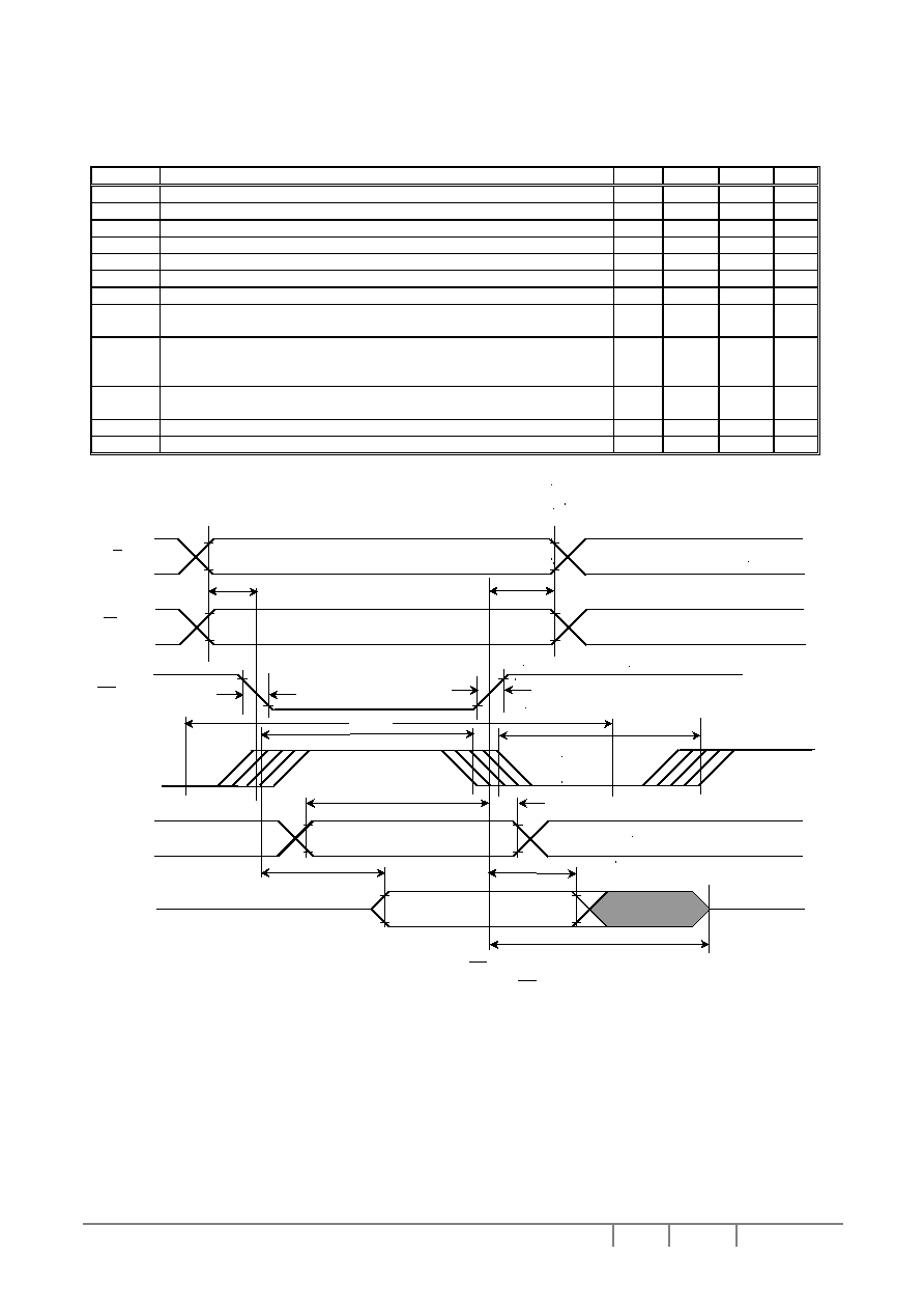
Solomon Systech
Jun 2004 P 40/52
Rev 1.1
SSD1805 Series
Table 16 - Parallel 6800-series Interface Timing Characteristics
(T
A
= -35 to 85
�C, V
DD
= V
CI
= 1.8V to 3.6V, V
DDIO
= 1.2V to V
DD
)
Symbol Parameter
Min Typ Max Unit
t
cycle
Clock Cycle Time
200
1000
-
ns
t
AS
Address Setup Time
0
-
25
ns
t
AH
Address Hold Time
0
-
-
ns
t
DSW
Write Data Setup Time
40
-
-
ns
t
DHW
Write Data Hold Time
10
-
-
ns
t
DHR
Read Data Hold Time
10
-
50
ns
t
OH
Output Disable Time
-
-
40
ns
t
ACC
Access Time (RAM)
Access Time (Command)
15
15
-
-
-
-
ns
ns
PW
CSL
Chip Select Low Pulse Width (read RAM)
Chip Select Low Pulse Width (read Command)
Chip Select Low Pulse Width (write)
500
500
100
-
-
-
-
-
-
ns
ns
ns
PW
CSH
Chip Select High Pulse Width (read)
Chip Select High Pulse Width (write)
200
100
-
-
-
-
ns
ns
t
R
Rise
Time
-
- 10
ns
t
F
Fall
Time
-
-
10
ns
The PW
CSH
timing reference is 50% of the rising / falling edge of E or CS pin.
The t
DSW
and t
DHW
timing is reference to the 50% of rising / falling edge of E or CS pin.
Figure 11 - Parallel 6800-series Interface Timing Characteristics (P/S = H, C68/80 = H)
t
cycle
D0~D7(Write)
D0~D7(Read)
CS
E
PW
CSH
t
R
t
F
t
DHW
t
OH
t
ACC
t
DHR
Valid Data
t
DSW
Valid Data
PW
CSL
W
/
R
t
AH
t
AS
C
/
D

SSD1805 Series
Rev 1.1
P 41/52
Jun 2004
Solomon Systech
Table 17 - Parallel 6800-series Interface Timing Characteristics
(T
A
= -35 to 85
�C, V
DD
= V
CI
= V
DDIO
= 1.8V to 3.6V)
Symbol Parameter
Min Typ Max Unit
t
cycle
Clock Cycle Time
100
500
-
ns
t
AS
Address Setup Time
0
-
25
ns
t
AH
Address Hold Time
0
-
-
ns
t
DSW
Write Data Setup Time
30
-
-
ns
t
DHW
Write Data Hold Time
5
-
-
ns
t
DHR
Read Data Hold Time
10
-
50
ns
t
OH
Output Disable Time
-
-
40
ns
t
ACC
Access Time (RAM)
Access Time (Command)
15
15
-
-
-
-
ns
ns
PW
CSL
Chip Select Low Pulse Width (read RAM)
Chip Select Low Pulse Width (read Command)
Chip Select Low Pulse Width (write)
250
250
50
-
-
-
-
-
-
ns
ns
ns
PW
CSH
Chip Select High Pulse Width (read)
Chip Select High Pulse Width (write)
100
50
-
-
-
-
ns
ns
t
R
Rise
Time
-
- 10
ns
t
F
Fall
Time
-
-
10
ns
The PW
CSH
timing reference is 50% of the rising / falling edge of E or CS pin.
The t
DSW
and t
DHW
timing is reference to the 50% of rising / falling edge of E or CS pin.
Figure 12 - Parallel 6800-series Interface Timing Characteristics (P/S = H, C68/80 = H)
t
cycle
D0~D7(Write)
D0~D7(Read)
CS
E
PW
CSH
t
R
t
F
t
DHW
t
OH
t
ACC
t
DHR
Valid Data
t
DSW
Valid Data
PW
CSL
W
/
R
t
AH
t
AS
C
/
D
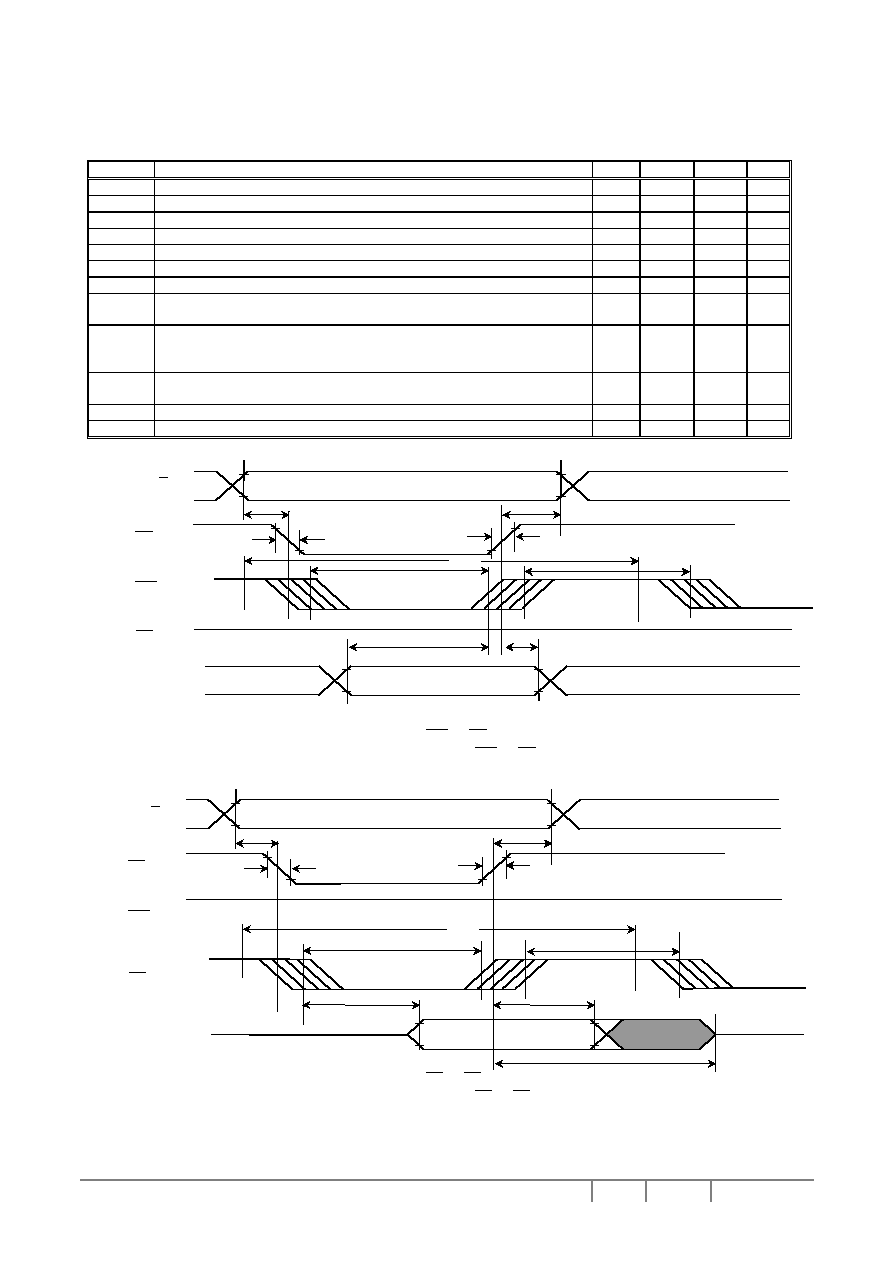
Solomon Systech
Jun 2004 P 42/52
Rev 1.1
SSD1805 Series
Table 18 - Parallel 8080-series Interface Timing Characteristics
(T
A
= -35 to 85
�C, V
DD
= V
CI
= 1.8V to 3.6V, V
DDIO
= 1.2V to V
DD
)
Symbol Parameter
Min Typ Max Unit
t
cycle
Clock Cycle Time
200
1000
-
ns
t
AS
Address Setup Time
0
-
25
ns
t
AH
Address Hold Time
0
-
-
ns
t
DSW
Write Data Setup Time
40
-
-
ns
t
DHW
Write Data Hold Time
10
-
-
ns
t
DHR
Read Data Hold Time
10
-
50
ns
t
OH
Output Disable Time
-
-
40
ns
t
ACC
Access Time (RAM)
Access Time (Command)
15
15
-
-
-
-
ns
ns
PW
CSL
Chip Select Low Pulse Width (read RAM)
Chip Select Low Pulse Width (read Command)
Chip Select Low Pulse Width (write)
500
500
100
-
-
-
-
-
-
ns
ns
ns
PW
CSH
Chip Select High Pulse Width (read)
Chip Select High Pulse Width (write)
200
100
-
-
-
-
ns
ns
t
R
Rise
Time
-
- 10
ns
t
F
Fall
Time
-
-
10
ns
The PW
CSL
timing reference is 50% of the rising / falling edge of WR or CS pin.
The t
DSW
and t
DHW
timing is reference to the 50% of rising / falling edge of WR or CS pin.
The PW
CSL
timing reference is 50% of the rising / falling edge of RD or CS pin.
The t
DSW
and t
DHW
timing is reference to the 50% of rising / falling edge of RD or CS pin.
Figure 13 - Parallel 8080-series Interface Timing Characteristics (P/S = H, C68/80 = L)
PW
CSH
PW
CSL
t
DSW
t
DHW
t
cycle
t
AH
t
AS
C
/
D
RD
CS
Valid Data
D0-D7(WRITE)
WR
t
R
t
F
Write Cycle
t
OH
t
ACC
Valid Data
t
DHR
D0-D7(READ)
PW
CSH
PW
CSL
t
AH
t
AS
C
/
D
CS
WR
t
R
t
F
RD
Read Cycle
t
cycle
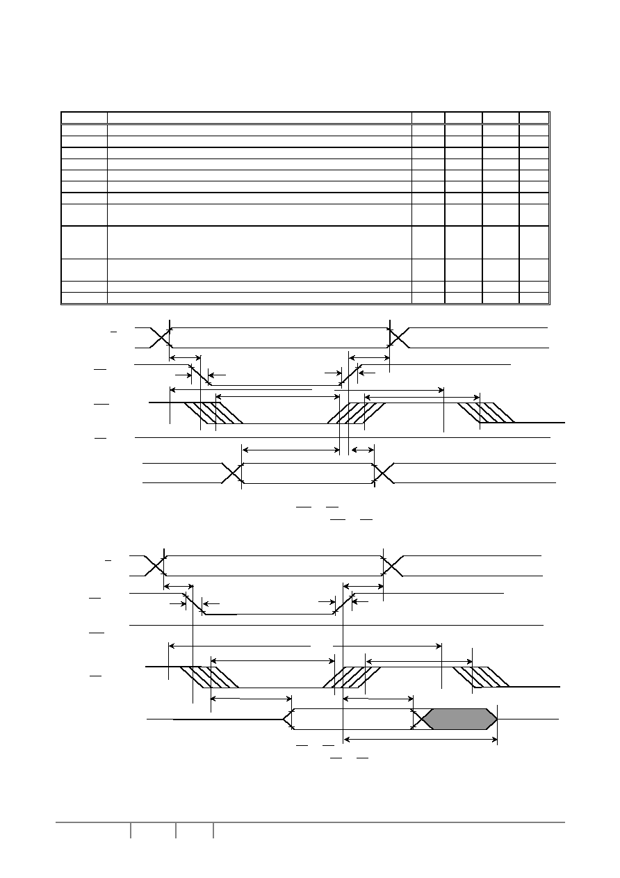
SSD1805 Series
Rev 1.1
P 43/52
Jun 2004
Solomon Systech
Table 19 - Parallel 8080-series Interface Timing Characteristics
(T
A
= -35 to 85
�C, V
DD
= V
CI
= V
DDIO
= 1.8V to 3.6V)
Symbol Parameter
Min Typ Max Unit
t
cycle
Clock Cycle Time
100
500
-
ns
t
AS
Address Setup Time
0
-
25
ns
t
AH
Address Hold Time
0
-
-
ns
t
DSW
Write Data Setup Time
30
-
-
ns
t
DHW
Write Data Hold Time
5
-
-
ns
t
DHR
Read Data Hold Time
10
-
50
ns
t
OH
Output Disable Time
-
-
40
ns
t
ACC
Access Time (RAM)
Access Time (Command)
15
15
-
-
-
-
ns
ns
PW
CSL
Chip Select Low Pulse Width (read RAM)
Chip Select Low Pulse Width (read Command)
Chip Select Low Pulse Width (write)
250
250
50
-
-
-
-
-
-
ns
ns
ns
PW
CSH
Chip Select High Pulse Width (read)
Chip Select High Pulse Width (write)
100
50
-
-
-
-
ns
ns
t
R
Rise
Time
-
- 10
ns
t
F
Fall
Time
-
-
10
ns
The PW
CSL
timing reference is 50% of the rising / falling edge of WR or CS pin.
The t
DSW
and t
DHW
timing is reference to the 50% of rising / falling edge of WR or CS pin.
The PW
CSL
timing reference is 50% of the rising / falling edge of RD or CS pin.
The t
DSW
and t
DHW
timing is reference to the 50% of rising / falling edge of RD or CS pin.
Figure 14 - Parallel 8080-series Interface Timing Characteristics (P/S = H, C68/80 = L)
PW
CSH
PW
CSL
t
DSW
t
DHW
t
cycle
t
AH
t
AS
C
/
D
RD
CS
Valid Data
D0-D7(WRITE)
WR
t
R
t
F
Write Cycle
t
OH
t
ACC
Valid Data
t
DHR
D0-D7(READ)
PW
CSH
PW
CSL
t
AH
t
AS
C
/
D
CS
WR
t
R
t
F
RD
Read Cycle
t
cycle
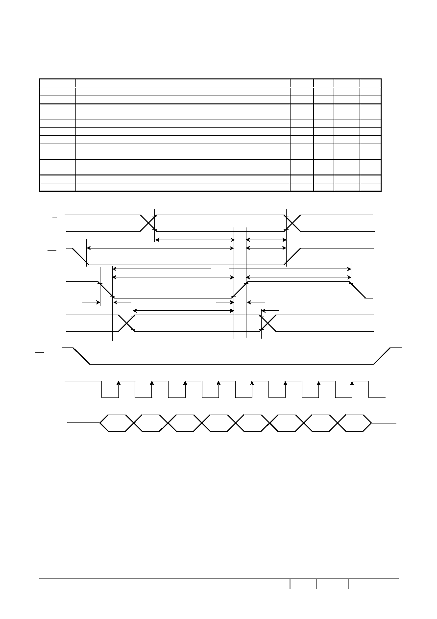
Solomon Systech
Jun 2004 P 44/52
Rev 1.1
SSD1805 Series
Table 20 - 4-wires Serial Interface Timing Characteristics
(T
A
= -35 to 85
�C, V
DD
= V
CI
= 1.8V to 3.6V, V
DDIO
= 1.2V to V
DD
)
Symbol Parameter
Min Typ Max Unit
t
cycle
Clock Cycle Time
111
-
-
ns
t
AS
Address Setup Time
15
-
-
ns
t
AH
Address Hold Time
10
-
-
ns
t
DSW
Write Data Setup Time
60
-
-
ns
t
DHW
Write Data Hold Time
60
-
-
ns
T
CLKL
Clock Low Time
55.5
-
-
ns
T
CLKH
Clock High Time
55.5
-
-
ns
t
CSS
Chip Select Setup Time (for D7 input)
60
-
-
-
-
ns
t
CSH
Chip Select Hold Time (for D0 input)
55.5
-
-
-
-
ns
t
R
Rise
Time
-
-
10
ns
t
F
Fall
Time
-
-
10
ns
Figure 15 - 4-wires Serial Interface Timing Characteristics (P/S = L, C68/80 = L)
t
AH
t
AS
C
/
D
Valid Data
t
DHW
t
CLKL
t
DSW
t
CLKH
t
cycle
t
CSS
t
CSH
t
F
t
R
SDA(D7)
CS
SCK(D6)
D7
SDA(D7)
CS
SCK(D6)
D6
D5
D4
D3
D2
D1
D0
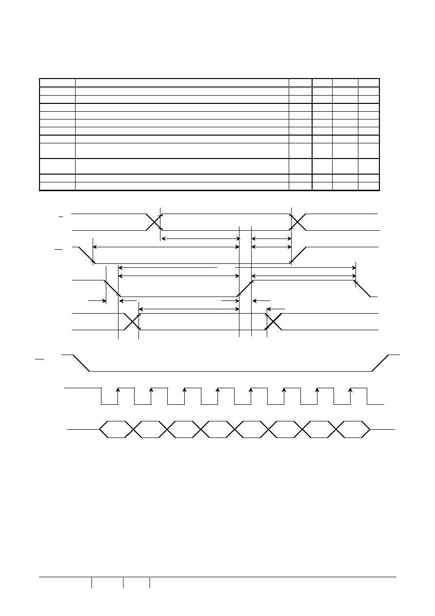
SSD1805 Series
Rev 1.1
P 45/52
Jun 2004
Solomon Systech
Table 21 - 4-wires Serial Interface Timing Characteristics
(T
A
= -35 to 85
�C, V
DD
= V
CI
= V
DDIO
= 1.8V to 3.6V)
Symbol
Parameter
Min Typ Max Unit
t
cycle
Clock Cycle Time
58.8
-
-
ns
t
AS
Address Setup Time
10
-
-
ns
t
AH
Address Hold Time
5
-
-
ns
t
DSW
Write Data Setup Time
30
-
-
ns
t
DHW
Write Data Hold Time
30
-
-
ns
T
CLKL
Clock Low Time
29.4
-
-
ns
T
CLKH
Clock High Time
29.4
-
-
ns
t
CSS
Chip Select Setup Time (for D7 input)
30
-
-
-
-
ns
t
CSH
Chip Select Hold Time (for D0 input)
29.4
-
-
-
-
ns
t
R
Rise
Time
-
-
10
ns
t
F
Fall
Time
-
-
10
ns
Figure 16 - 4-wires Serial Interface Timing Characteristics (P/S = L, C68/80 = L)
t
AH
t
AS
C
/
D
Valid Data
t
DHW
t
CLKL
t
DSW
t
CLKH
t
cycle
t
CSS
t
CSH
t
F
t
R
SDA(D7)
CS
SCK(D6)
D7
SDA(D7)
CS
SCK(D6)
D6
D5
D4
D3
D2
D1
D0
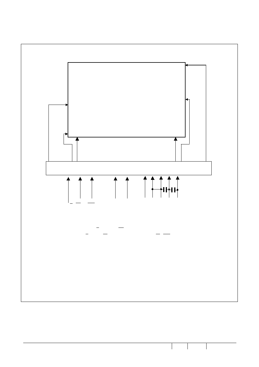
Solomon Systech
Jun 2004 P 46/52
Rev 1.1
SSD1805 Series
13 APPLICATION EXAMPLES
Figure 17 - Application Example I (4-wires SPI mode)
,where
V
DD
& V
CI
= 2.775V; V
DDIO
= 2.775V;
C
1
= 1uF ~2uF; C
2
= 2.2uF ~ 4.7uF.
Logic pin connections not specified above:
Pins connected to V
DD
: IRS; M/
S
; CLS; E(
RD
); CS2; /HPM;
Pins connected to V
SS
: P/
S
; C68/(
80
); V
SS1
; V
LREF
; D0~D5; R/
W
(
WR
); TEST0;
Pin connected to V
OUT
: V
HREF
;
Pins connected to Either V
DD
or V
SS
depending on configuration: C0; C1; B0; B1;
CS
RES
C
/
D
COL0 ................................................................................................. COL131
ROW67 .......ROW34
ROW33 ................ROW0
S
E
G
131
S
E
G
130
S
E
G
129
S
E
G
128
S
E
G
127
S
E
G
126
:
:
:
:
:
:
:
:
:
:
:
:
:
:
:
:
:
:
:
SEG
5
SEG
4
SEG
3
SEG
2
SEG
1
SEG
0
COM34
COM35
:
:
:
:
:
:
:
COM66
COM67
COM0
COM1
:
:
:
:
:
:
:
COM32
COM33
Row remapped
command
[command: C0H]
DISPLAY PANEL SIZE
132 X 68
SSD1805 IC (DIE FACE UP)
SCK SDA
C
1
C
2
V
DD
V
CI
V
SS
V
OUT
V
DDIO
Software initialization (For 68 MUX application)
E2 //Software reset
2F //Turn on regulated charge-pump and divider
86 //Set 5X booster configuration
24 //Set internal resistor gain to 24Hex
81 //Set contrast level to 20Hex
20 //
A2 //Set normal bias ratio as 1/9 bias
AF //Set Display On
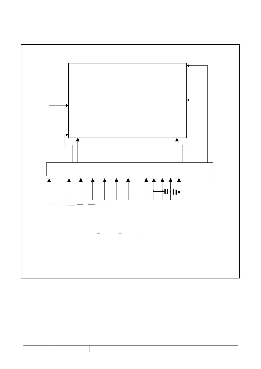
SSD1805 Series
Rev 1.1
P 47/52
Jun 2004
Solomon Systech
Figure 18 - Application Example II (6800 PPI mode)
,where
V
DD
& V
CI
= 2.775V; V
DDIO
= 2.775V;
C
1
= 1uF ~2uF; C
2
= 2.2uF ~ 4.7uF.
Logic pin connections not specified above:
Pins connected to V
DD
: IRS; M/
S
; CLS; P/
S
; C68/(
80
); CS2; /HPM;
Pins connected to V
SS
: V
SS1
; V
LREF
; TEST0;
Pin connected to V
OUT
: V
HREF
;
Pins connected to Either V
DD
or V
SS
depending on configuration: C0; C1; B0;
B1;
CS
RES
C
/
D
COL0 ................................................................................................. COL131
ROW67 .......ROW34
ROW33 ................ROW0
SEG
1
3
1
SEG
1
3
0
SEG
1
2
9
SEG
1
2
8
SEG
1
2
7
SEG
1
2
6
:
:
:
:
:
:
:
:
:
:
:
:
:
:
:
:
:
:
:
SEG
5
SEG
4
SEG
3
SEG
2
SEG
1
SEG
0
COM34
COM35
:
:
:
:
:
:
:
COM66
COM67
COM0
COM1
:
:
:
:
:
:
:
COM32
COM33
Row remapped
command
[command: C0H]
DISPLAY PANEL SIZE
132 X 68
SSD1805 IC (DIE FACE UP)
D0 ... D7
C
1
C
2
V
DD
V
CI
V
SS
V
OUT
V
DDIO
E( RD )
R/W ( WR )
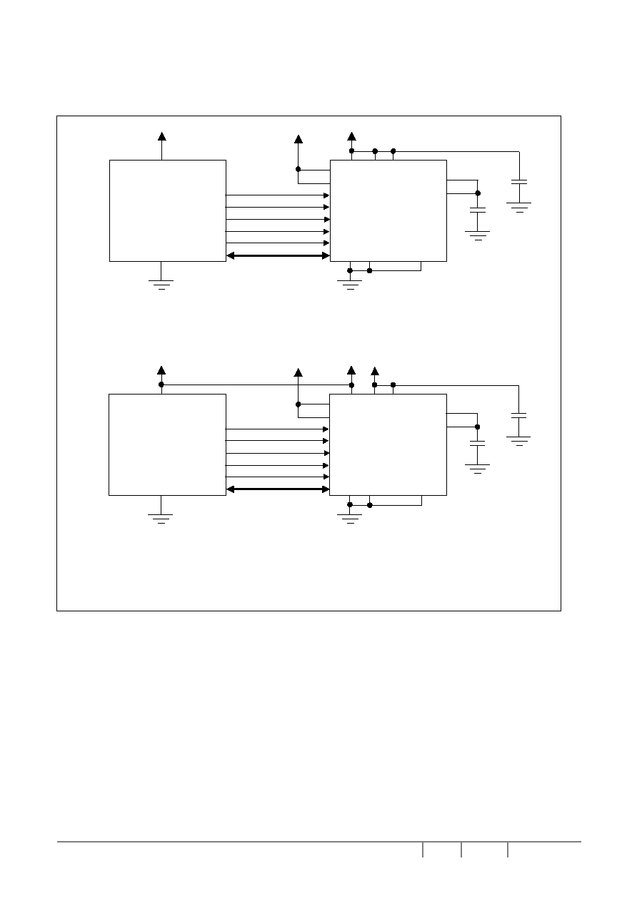
Solomon Systech
Jun 2004 P 48/52
Rev 1.1
SSD1805 Series
Figure 19 - Applications notes for V
DD
/V
DDIO
connection
MCU
SSD1805
/CS1
/RES
D/C
R/W
E
D0~D7
V
OUT
V
HREF
2.775V
2.775V
2.775V
V
DDIO
V
DD
V
CI
CLS
M/S
MCU
SSD1805
/CS1
/RES
D/C
R/W
E
D0~D7
V
OUT
V
HREF
1.8V
2.775V
or 1.8V
1.8V
V
DDIO
V
DD
V
CI
CLS
M/S
2.775V
Normal Application
Low Voltage MCU
V
SS
V
SS1
V
LREF
V
SS
V
SS1
V
LREF
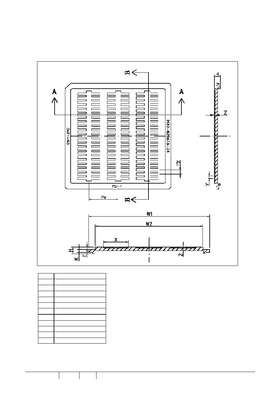
SSD1805 Series
Rev 1.1
P 49/52
Jun 2004
Solomon Systech
14 PACKAGE INFORMATION
14.1 DIE TRAY DIMENSIONS
Spec mm
(mil)
W1
50.70
� 0.2
(1996)
W2
45.50
� 0.2
(1791)
H
4.05
� 0.2
(160)
K N/A
E N/A
Px
14.19
� 0.1
(559)
Py
2.48
� 0.1
(98)
X
11.26 + 0.1
(443)
Y
1.41 + 0.1
(58)
Z
0.68
� 0.05
(27)
N 51
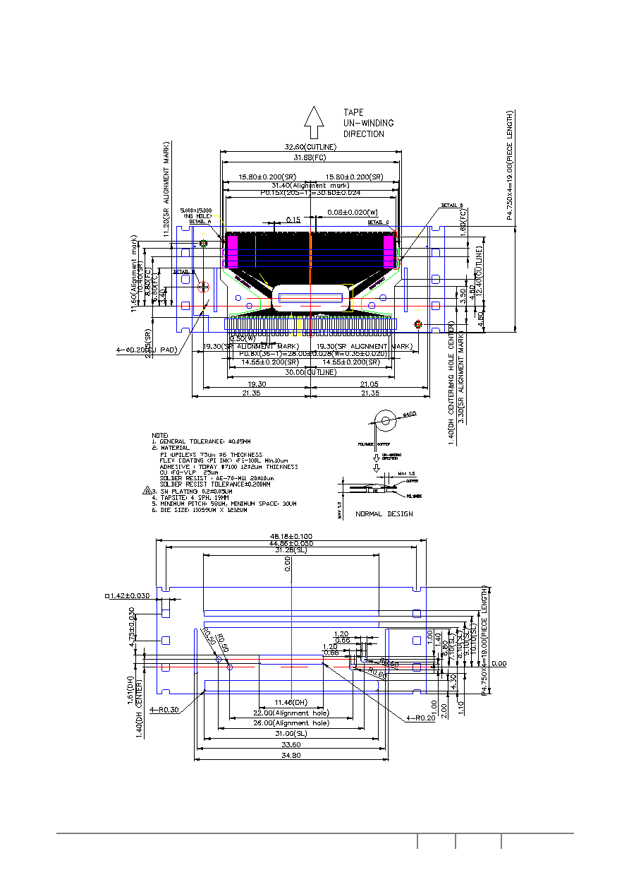
Solomon Systech
Jun 2004 P 50/52
Rev 1.1
SSD1805 Series
14.2 TAB DRAWING
Figure 20 - SSD1805TR1 TAB Drawing (Copper view)

SSD1805 Series
Rev 1.1
P 51/52
Jun 2004
Solomon Systech
Figure 21 - SSD1805TR1 TAB Drawing (Detail view & pin assignment)
34 33 32 31 30 29 28 27 26 25 24 23 22 21 20 19 18 17 16 15 14 13 12 11 10 9 8 7 6 5 4 3 2 1

Solomon Systech
Jun 2004 P 52/52
Rev 1.1
SSD1805 Series
Solomon Systech reserves the right to make changes without further notice to any products herein. Solomon Systech makes no warranty,
representation or guarantee regarding the suitability of its products for any particular purpose, nor does Solomon Systech assume any liability arising
out of the application or use of any product or circuit, and specifically disclaims any and all liability, including without limitation consequential or
incidental damages. "Typical" parameters can and do vary in different applications. All operating parameters, including "Typicals" must be validated for
each customer application by customer's technical experts. Solomon Systech does not convey any license under its patent rights nor the rights of
others. Solomon Systech products are not designed, intended, or authorized for use as components in systems intended for surgical implant into the
body, or other applications intended to support or sustain life, or for any other application in which the failure of the Solomon Systech product could
create a situation where personal injury or death may occur. Should Buyer purchase or use Solomon Systech products for any such unintended or
unauthorized application, Buyer shall indemnify and hold Solomon Systech and its offices, employees, subsidiaries, affiliates, and distributors harmless
against all claims, costs, damages, and expenses, and reasonable attorney fees arising out of, directly or indirectly, any claim of personal injury or
death associated with such unintended or unauthorized use, even if such claim alleges that Solomon Systech was negligent regarding the design or
manufacture of the part
http://www.solomon-systech.com