 | –≠–ª–µ–∫—Ç—Ä–æ–Ω–Ω—ã–π –∫–æ–º–ø–æ–Ω–µ–Ω—Ç: SSD1809 | –°–∫–∞—á–∞—Ç—å:  PDF PDF  ZIP ZIP |

This document contains information on a new product under definition stage. Solomon Systech Ltd. reserves the
right to change or discontinue this product without notice.
http://www.solomon-systech.com
SSD1809
Rev 1.3
Mar 2002
Copyright
©
2003
Solomon Systech Limited
SOLOMON SYSTECH
SEMICONDUCTOR TECHNICAL DATA
P 1/27
LCD Segment / Common Driver
With Controller
CMOS
SSD1809 is a single-chip CMOS LCD driver with controller for liquid
crystal dot-matrix graphic display system. It consists of 225 high voltage
driving output pins for driving 160 Segments, 64 Commons and 1icon driv-
ing-Common.
SSD1809 displays data directly from its internal Graphic RAM
(160x65). Data/Commands are sent from general MCU through a software
selectable 6800-/8080-series compatible Parallel Interface or Serial Periph-
eral Interface.
SSD1809 embeds a DC-DC Converter, an On-chip Bias Divider and an
On-Chip Oscillator which reduce the number of external components. With
the special design on minimizing power consumption and package layout,
SSD1809 is suitable for any portable battery-driven application requiring a
long operation period and a compact size.
∑
160x64 Graphic Display with a Icon Line
∑
Programmable Multiplex Ratio (1 Mux - 65 Mux) [Partial Display]
∑
Graphic Display Mode Operation / Chinese Character Display Mode Operation
∑
Supply Operation, 2.2 V - 3.5 V
∑
Enhanced Low Power Icon Mode (160 icons, <19uA)
∑
On-Chip Internal DC-DC Converter / External Power Supply
∑
2X / 3X / 4X / 5X DC-DC Converter
∑
On-Chip Oscillator
∑
On-Chip Bias Voltage Generator
∑
1:5 / 1:7 / 1:8 / 1:9 Bias Ratio
∑
Maximum 16.5V LCD Driving Output Voltage
∑
8-bit 6800-Series Parallel Interface, 8-bit 80-Series Parallel Interface and Serial
Peripheral Interface (SPI)
∑
On-Chip 160 x 65 Display Data RAM
∑
Re-mapping of Row and Column Drivers
∑
Vertical Scrolling
∑
Display Masks for implementation of blinking effect
∑
Programmable Frame Frequency
∑
Master Clear RAM
∑
External Contrast Control
∑
16 Level Internal Contrast Control
∑
Selectable LCD Driving Voltage Temperature Coefficients
∑
Available in TAB (Tape Automated Bonding)
SSD1809
ORDERING INFORMATION
SSD1809TR
TAB
SSD1809TR
TAB

SSD1809
Rev 1.3
Mar 2002
Solomon Systech
P 2/27
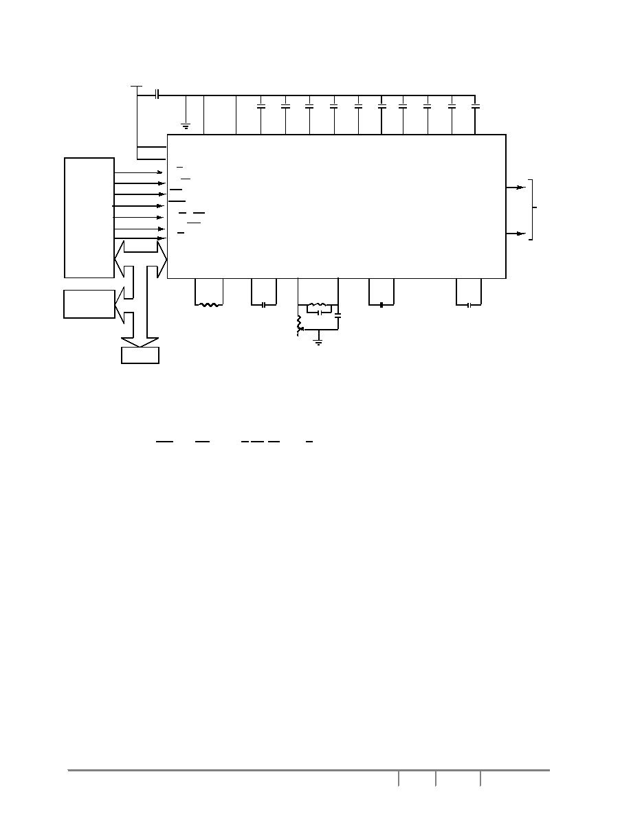
Block Diagram
Voltage
Divider
SEG0 ~ SEG159
OSC1
OSC2
RES
R/W / RD
SDA/D0,D1~D7
V
LL2
~ V
LL6
V
CC
V
R
V
F
C
1P
~ C
3P
C
1N
~ C
3N
DUM1 ~ DUM4
C+
C-
AV
DD
AV
SS
GDDRAM
65x 160 Bits
Command
Decoder
Display
Timing
Generator
160 Bit Latch
65 Bit
Latch
HV Buffer Cell Level Shifter
Level
Selector
CLK / W R / S C K
D/C
Command/Data Interface
Control Logic
DV
DD
DV
SS
Temperature
Compensation
Contrast
Control
Voltage
Regulator
2X/3X/4X/5X
DC-DC
Converter
P/S
68/80
CE
COM0 ~ COM64
V
DC
Solomon Systech
Mar 2002
Rev 1.3
SSD1809
P 3/27
P 3/27
P 3/27
P 3/27
P 3/27
P 3/27
P 3/27
P 3/27
P 3/27
P 3/27
P 3/27
P 3/27
1 2
3
4 5
6
7 8
9
1
0 11 12 13 14 15 16 17 18 19 20 21 22 23 24 25 26 27 28 29 30 31 32 33 34 35 36 37 38 39 40 41 42 43 44 45 46 47 48
V
D
C
D
V
D
D
R
E
S
D
/
C
R
/
W
/
R
D
C
L
K
/
/
W
R
/
S
C
K
D
V
S
S
S
D
A
/
D
0
D
1
D
2
D
3
D
4
D
5
D
6
D
7
C
E
C
1
P
C
1
N
C
2
P
C
2
N
C
3
P
C
3
N
N
C
N
C
D
V
S
S
V
L
L
2
V
L
L
3
D
U
M
4
D
U
M
3
D
U
M
2
D
V
S
S
D
U
M
1
D
V
S
S
V
L
L
4
V
L
L
5
V
L
L
6
O
S
C
1
D
V
S
S
C
+
C
-
V
C
C
V
F
V
R
A
V
S
S
O
S
C
2
A
V
D
D
P
/
S
6
8
/
8
0
C
O
M
3
1
C
O
M
3
0
C
O
M
2
9
C
O
M
2
C
O
M
1
C
O
M
0
C
O
M
6
4
S
E
G
1
5
9
S
E
G
1
5
8
S
E
G
1
5
7
S
E
G
8
2
S
E
G
8
1
S
E
G
8
0
2
7
4
2
7
3
2
7
2
2
4
5
2
4
4
2
4
3
2
4
2
2
4
1
2
4
0
2
3
9
1
6
4
1
6
3
1
6
2
S
E
G
7
9
S
E
G
7
8
S
E
G
7
7
S
E
G
2
S
E
G
1
S
E
G
0
C
O
M
3
2
C
O
M
3
3
C
O
M
3
4
C
O
M
3
5
C
O
M
6
2
C
O
M
6
3
C
O
M
6
4
1
6
1
1
6
0
1
5
9
8
4 83 82 81 80 79 78
5
1
5
0
4
9
D
U
M
M
Y
D
U
M
M
Y
D
U
M
M
Y
D
U
M
M
Y
D
U
M
M
Y
D
U
M
M
Y
D
U
M
M
Y
D
U
M
M
Y
*
*
D
U
M
M
Y
Normal Design TAB
DIE
ENCAPSULANT
COPPER
POLYIMIDE
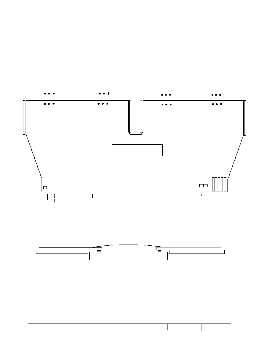
SSD1809T PIN ASSIGNMENT
(COPPER VIEW)
*Remarks: In the TAB package, pin1(VDC) & pin2(DVDD) are connected to DVDD. Pin46(AVDD), pin47(P/S) & pin48(68/80) are connected to AVDD.

SSD1809
Rev 1.3
Mar 2002
Solomon Systech
P 4/27
SSD1809T Pin Assignment Table
TAB
Pin #
Signal Name
TAB
Pin #
Signal Name
TAB
Pin #
Signal Name
TAB
Pin #
Signal Name
TAB
Pin #
Signal Name
1
2
3
4
5
6
7
8
9
10
11
12
13
14
15
16
17
18
19
20
21
22
23
24
25
26
27
28
29
30
31
32
33
34
35
36
37
38
39
40
41
42
43
44
45
46
47
48
49
50
51
52
53
54
55
56
57
58
59
60
V
DC
DV
DD
RES
D/C
R/W / RD
CLK/WR/SCK
DV
SS
SDA/D
0
D
1
D
2
D
3
D
4
D
5
D
6
D
7
CE
C
1 P
C
1 N
C
2 P
C
2 N
C
3 P
C
3 N
NC
NC
DV
SS
V
LL2
V
LL3
DUM4
DUM3
DUM2
DV
SS
DUM1
DV
SS
V
LL4
V
LL5
V
LL6
OSC1
DV
SS
C+
C-
V
CC
V
F
V
R
AV
SS
OSC2
AV
D D
P/S
68/80
COM64
COM63
COM62
COM61
COM60
COM59
COM58
COM57
COM56
COM55
COM54
COM53
61
62
63
64
65
66
67
68
69
70
71
72
73
74
75
76
77
78
79
80
81
82
83
84
85
86
87
88
89
90
91
92
93
94
95
96
97
98
99
100
101
102
103
104
105
106
107
108
109
110
111
112
113
114
115
116
117
118
119
120
COM52
COM51
COM50
COM49
COM48
COM47
COM46
COM45
COM44
COM43
COM42
COM41
COM40
COM39
COM38
COM37
COM36
COM35
COM34
COM33
COM32
SEG0
SEG1
SEG2
SEG3
SEG4
SEG5
SEG6
SEG7
SEG8
SEG9
SEG10
SEG11
SEG12
SEG13
SEG14
SEG15
SEG16
SEG17
SEG18
SEG19
SEG20
SEG21
SEG22
SEG23
SEG24
SEG25
SEG26
SEG27
SEG28
SEG29
SEG30
SEG31
SEG32
SEG33
SEG34
SEG35
SEG36
SEG37
SEG38
121
122
123
124
125
126
127
128
129
130
131
132
133
134
135
136
137
138
139
140
141
142
143
144
145
146
147
148
149
150
151
152
153
154
155
156
157
158
159
160
161
162
163
164
165
166
167
168
169
170
171
172
173
174
175
176
177
178
179
180
SEG39
SEG40
SEG41
SEG42
SEG43
SEG44
SEG45
SEG46
SEG47
SEG48
SEG49
SEG50
SEG51
SEG52
SEG53
SEG54
SEG55
SEG56
SEG57
SEG58
SEG59
SEG60
SEG61
SEG62
SEG63
SEG64
SEG65
SEG66
SEG67
SEG68
SEG69
SEG70
SEG71
SEG72
SEG73
SEG74
SEG75
SEG76
SEG77
SEG78
SEG79
SEG80
SEG81
SEG82
SEG83
SEG84
SEG85
SEG86
SEG87
SEG88
SEG89
SEG90
SEG91
SEG92
SEG93
SEG94
SEG95
SEG96
SEG97
SEG98
181
182
183
184
185
186
187
188
189
190
191
192
193
194
195
196
197
198
199
200
201
202
203
204
205
206
207
208
209
210
211
212
213
214
215
216
217
218
219
220
221
222
223
224
225
226
227
228
229
230
231
232
233
234
235
236
237
238
239
240
SEG99
SEG100
SEG101
SEG102
SEG103
SEG104
SEG105
SEG106
SEG107
SEG108
SEG109
SEG110
SEG111
SEG112
SEG113
SEG114
SEG115
SEG116
SEG117
SEG118
SEG119
SEG120
SEG121
SEG122
SEG123
SEG124
SEG125
SEG126
SEG127
SEG128
SEG129
SEG130
SEG131
SEG132
SEG133
SEG134
SEG135
SEG136
SEG137
SEG138
SEG139
SEG140
SEG141
SEG142
SEG143
SEG144
SEG145
SEG146
SEG147
SEG148
SEG149
SEG150
SEG151
SEG152
SEG153
SEG154
SEG155
SEG156
SEG157
SEG158
241
242
243
244
245
246
247
248
249
250
251
252
253
254
255
256
257
258
259
260
261
262
263
264
265
266
267
268
269
270
271
272
273
274
SEG159
COM64
COM0
COM1
COM2
COM3
COM4
COM5
COM6
COM7
COM8
COM9
COM10
COM11
COM12
COM13
COM14
COM15
COM16
COM17
COM18
COM19
COM20
COM21
COM22
COM23
COM24
COM25
COM26
COM27
COM28
COM29
COM30
COM31
Solomon Systech
Mar 2002
Rev 1.3
SSD1809
P 5/27
P 5/27
P 5/27
P 5/27
P 5/27
P 5/27
P 5/27
P 5/27
P 5/27
P 5/27
P 5/27
P 5/27
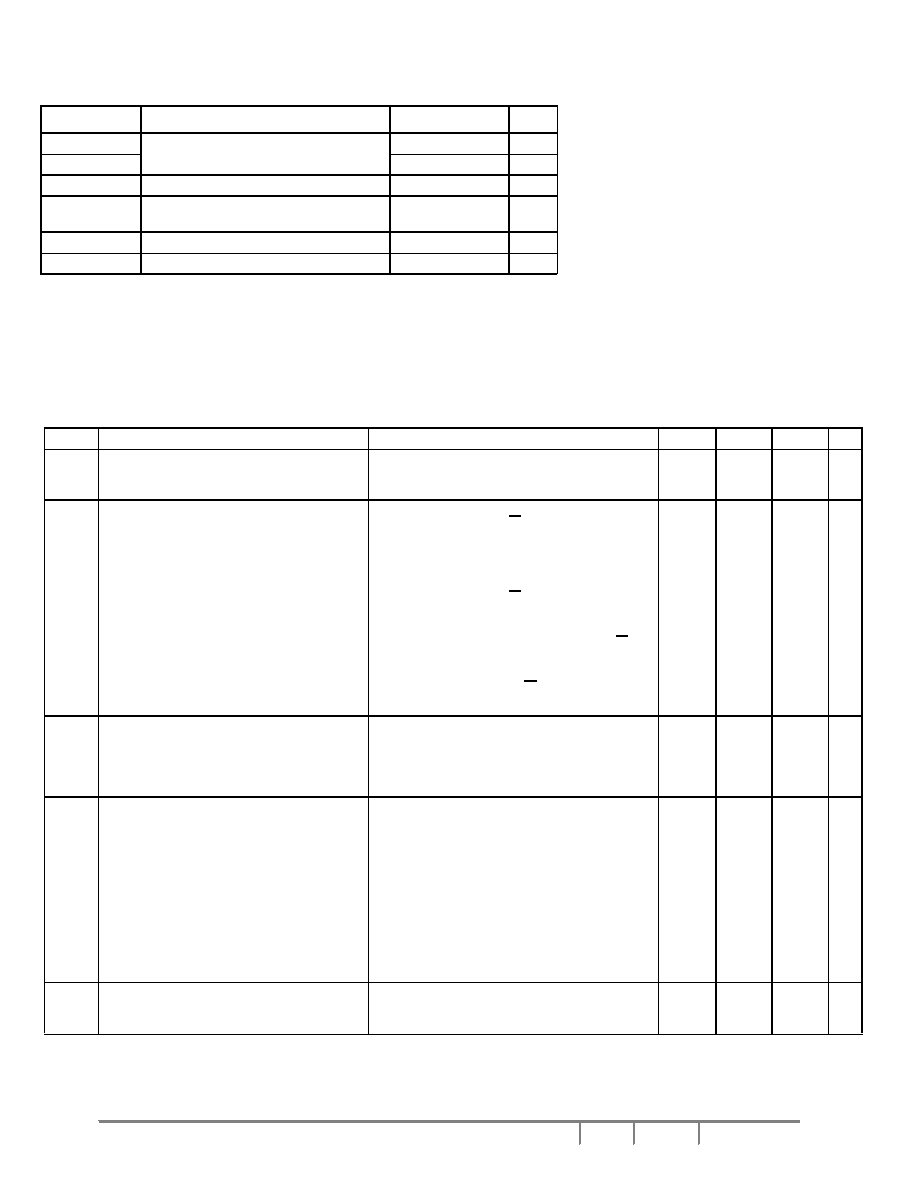
MAXIMUM RATINGS*
(Voltages Referenced to V
SS
, T
A
=25∞C)
Symbol
Parameter
Value
Unit
AV
DD
,DV
DD
,V
DC
Supply Voltage
-0.3 to +4.0
V
V
CC
V
SS
-0.3 to V
SS
+18
V
V
in
Input Voltage
V
SS
-0.3 to V
DD
+0.3
V
I
Current Drain Per Pin Excluding V
DD
and
V
SS
25
mA
T
A
Operating Temperature
-30 to +85
∞C
T
stg
Storage Temperature Range
-65 to +150
∞C
* Maximum Ratings are those values beyond which damage to the device may occur. Functional
operation should be restricted to the limits in the Electrical Characteristics tables or Pin Descrip-
tion section.
V
SS
= AV
SS
= DV
SS
(DV
SS
= V
SS
of Digital circuit, AV
SS
= V
SS
of Analogue Circuit)
V
DD
= AV
DD
= DV
DD
(DV
DD
= V
D D
of Digital circuit, AV
DD
= V
DD
of Analogue Circuit)
This device contains circuitry to protect the inputs
against damage due to high static voltages or elec-
tric fields; however, it is advised that normal precau-
tions to be taken to avoid application of any voltage
higher than maximum rated voltages to this high
impedance circuit. For proper operation it is recom-
mended that V
in
and V
out
be constrained to the
range V
SS
< or = (V
in
or V
out
) < or = V
D D
. Reliability
of operation is enhanced if unused input are con-
nected to an appropriate logic voltage level (e.g.,
either V
SS
o r V
DD
). Unused outputs must be left
open. This device may be light sensitive. Caution
should be taken to avoid exposure of this device to
any light source during normal operation. This
device is not radiation protected.
ELECTRICAL CHARACTERISTICS
(Voltage Referenced to V
SS
, V
DD
=2.2 to 3.5V, T
A
=25∞C; unless otherwise specified.)
Symbol
Parameter
Test Condition
Min
Typ
Max
Unit
DV
DD
A V
DD
V
DC
Logic Circuit Supply Voltage Range
Voltage Generator Circuit Supply Voltage Range
DC/DC Converter Circuit Supply Voltage Range
(Absolute value referenced to V
SS
)
2.2
2.2
2.2
3.0
-
-
3.5
3.5
3.5
V
V
V
I
AC
I
DP
I
SB
I
ICON
Access Mode Supply Current Drain
(AV
DD
+ DV
DD
+ V
DC
Pins)
Display Mode Supply Current Drain
(AV
DD
+ DV
DD
Pins)
Standby Mode Supply Current Drain
(AV
DD
+ DV
DD
Pins)
Icon Mode Supply Current Drain
(AV
DD
+ DV
DD
Pins)
V
DD
=3.0V, Voltage Generator On, 5X Converter
Enabled, 65Mux Ratio, R/W accessing,
T
cyc
=200kHz, Internal Oscillator Enabled, Frame
Freq.=60Hz, Display On.
V
DD
=3.0V, Voltage Generator On, 5X Converter
Enabled, 65Mux Ratio, R/W Halt, Internal Oscillator
Enabled, Frame Freq.=60Hz, Display On.
V
DD
=3.0V, Display Off, Oscillator Disabled, R/W halt.
V
DD
=3.0V, Internal Oscillator Enabled, 65Mux Ratio,
Display On, Icon Mode C, R/W halt, Frame Freq.=
81.25Hz
-
-
-
-
-
170
-
11
450
270
1
19
µ
A
µ
A
µ
A
µ
A
V
CC
V
LCD
LCD Driving Voltage Generator Output
(V
CC
Pin)
LCD Driving Voltage Input (V
CC
Pin)
Display On, Voltage Generator Enabled,
DC/DC Converter Enabled, Frame Freq.=60Hz,
Voltage Regulator Enabled, Voltage Divider Enabled.
Voltage Generator Disabled, 1:5 Bias.
5
5
-
-
16.5
16.5
V
V
V
OH1
V
OL1
V
R1
V
R3
V
R2
Output High Voltage
(SDA/D
0
-D
7
, OSC2)
Output Low Voltage
(SDA/D
0
-D
7
, OSC2)
LCD Driving Voltage Source (V
R
Pin)
LCD Driving Voltage Source (V
R
Pin)
LCD Driving Voltage Source (V
R
Pin)
I
out
=100mA
I
out
=100mA
Voltage Regulator Enabled (V
R
voltage depends on
TC and Int/Ext Contrast Control )
Regulated DC/DC Converter Mode
Voltage Regulator & Regulated DC/DC Disabled.
0.9*V
DD
0
0
-
-
-
-
-
V
CC
Floating
V
DD
0.1*V
D D
V
CC
-0.5
-
-
V
V
V
V
V
V
CN
Internal Contrast Control
(V
R
Output Voltage)
Voltage Regulator Enabled, Internal Contrast control
Enabled. (16 Voltage Levels Controlled by Software.
)
-5
-
5
%

SSD1809
Rev 1.3
Mar 2002
Solomon Systech
P 6/27
ELECTRICAL CHARACTERISTICS
(Voltage Referenced to V
SS
, V
DD
=2.2 to 3.5V, T
A
=25∞C; unless otherwise specified.)
*The formula for the temperature coefficient (TC) is:
Symbol
Parameter
Test Condition
Min
Typ
Max
Unit
V
IH1
V
IL1
Input high voltage
(RES, OSC2, CLK/WR/SCK,SDA/D
0
-D
7
, CE ,
R/W/RD, D/C, P/S, 68/80, OSC1)
Input Low voltage
(RES, OSC2, CLK/WR/SCK,SDA/D
0
-D
7
, CE ,
R/W/RD, D/C, P/S, 68/80, OSC1)
0.8*V
DD
0
-
-
V
DD
0.2*V
DD
V
V
V
LL6
V
LL5
V
LL4
V
LL3
V
LL2
V
LL6
V
LL5
V
LL4
V
LL3
V
LL2
V
LL6
V
LL5
V
LL4
V
LL3
V
LL2
V
LL6
V
LL5
V
LL4
V
LL3
V
LL2
V
LL6
V
LL5
V
LL4
V
LL3
V
LL2
LCD Display Voltage Output
(V
LL6
, V
LL5
, V
LL4
, V
LL3
, V
LL2
Pins)
LCD Display Voltage Output
(V
LL6
, V
LL5
, V
LL4
, V
LL3
, V
LL2
Pins)
LCD Display Voltage Input
(V
LL6
, V
LL5
, V
LL4
, V
LL3
, V
LL2
Pins)
LCD Display Voltage Input
(V
LL6
, V
LL5
, V
LL4
, V
LL3
, V
LL2
Pins)
LCD Display Voltage Input
(V
LL6
, V
LL5
, V
LL4
, V
LL3
, V
LL2
Pins)
Voltage Divider Enabled, 1:5 bias ratio
Voltage Divider Enabled, 1:7 bias ratio
Voltage Divider Enabled, 1:8 bias ratio
Voltage Divider Enabled, 1:9 bias ratio
External Voltage Generator, Voltage Divider Disable
-
-
-
-
-
-
-
-
-
-
-
-
-
-
-
-
-
-
-
-
7
0
0
0
0
V
R
4/5*V
R
3/5*V
R
2/5*V
R
1/5*V
R
V
R
6/7*V
R
5/7*V
R
2/7*V
R
1/7*V
R
V
R
7/8*V
R
6/8*V
R
2/8*V
R
1/8*V
R
V
R
8/9*V
R
7/9*V
R
2/9*V
R
1/9*V
R
-
-
-
-
-
-
-
-
-
-
-
-
-
-
-
-
-
-
-
-
-
-
-
-
-
V
CC
V
LL6
V
LL5
V
LL4
V
LL3
V
V
V
V
V
V
V
V
V
V
V
V
V
V
V
V
V
V
V
V
V
V
V
V
V
I
O H
I
OL
I
O Z
Output High Current Source
(SDA/D
0
-D
7
, OSC2)
Output Low Current Drain
(SDA/D
0
-D
7
, OSC2)
Output Tri-state Current Drain Source
(SDA/D
0
-D
7
, OSC2)
V
out
=V
DD
-0.4V
V
out
=0.4V
50
-
-1
-
-
-
-
-50
1
µ
A
µ
A
µ
A
I
IL
/I
IH
Input Current
(RES, OSC2, CLK/WR/SCK,SDA/D
0
-D
7
, CE ,
R/W/RD, D/C, P/S, 68/80, OSC1)
-1
-
1
µ
A
R
on
Channel resistance between LCD driving signal
pins (SEG and COM) and driving voltage input
pins (V
LL2
to V
LL6
)
During Display on, 0.1V apply between two termi-
nals, V
CC
within operating voltage range
-
-
10
k
V
SB
Memory Retention Voltage (DV
DD
)
Standby mode, retain all internal configuration and
RAM data
2
-
-
V
C
IN
Input Capacitance
(OSC1, OSC2, all logic pins)
-
5
7.5
pF
PTC0
PTC3
Temperature Coefficient Compensation*
Flat Temperature Coefficient
Temperature Coefficient 3*
TC1=0, TC2=0, Voltage Regulator Disabled
TC1=1, TC2=1, Voltage Regulator Enabled
-
-
0.0
-0.35
-
-
%
%
TC(%)=
V
R
at 50∞C - V
R
at 0∞C
50∞C - 0∞C
X
1
V
R
at 25∞C
X 100%

Solomon Systech
Mar 2002
Rev 1.3
SSD1809
P 7/27
P 7/27
P 7/27
P 7/27
P 7/27
P 7/27
P 7/27
P 7/27
P 7/27
P 7/27
P 7/27
P 7/27
Figure 1 : Internal Oscillator Frequency Relationship with External Resistor Value at V
DD
= 3V
AC ELECTRICAL CHARACTERISTICS (Voltage Referenced to V
SS
, V
DD
=2.2 to 3.5V, T
A
=25∞C; unless otherwise specified.)
Symbol
Parameter
Test Condition
Min
Typ
Max
Unit
F
OSC
Oscillation Frequency of Display timing
generator
Resistor between OSC1 andOSC2 is 900k W
Internal Oscillator Enabled
-
50
-
kHz
F
FRM
Frame Frequency in Graphic / Charac-
ter Display Mode
Frame Frequency in Low Power Icon
Mode
Normal Display Frequency
Half Display Frequency
Icon Mode A and Normal Display Frequency
Icon Mode B and Normal Display Frequency
Icon Mode C and Normal Display Frequency
Icon Mode D and Normal Display Frequency
Icon Mode A and Half Display Frequency
Icon Mode B and Half Display Frequency
Icon Mode C and Half Display Frequency
Icon Mode D and Half Display Frequency
Fosc / [2 x Mux Ratio x (Frame Freq Register + 1)]
Fosc / [4 x Mux Ratio x (Frame Freq Register + 1)]
Fosc / [48 x (Frame Freq Register + 1)]
Fosc / [64 x (Frame Freq Register + 1)]
Fosc / [96 x (Frame Freq Register + 1)]
Fosc / [144 x (Frame Freq Register + 1)]
Fosc / [96 x (Frame Freq Register +1)]
Fosc / [128 x (Frame Freq Register + 1)]
Fosc / [192 x (Frame Freq Register + 1)]
Fosc / [288 x (Frame Freq Register + 1)]
OSC
Internal Oscillation Frequency with dif-
ferent value of feedback resistor
Internal Oscillator Enabled, V
DD
within oper-
ation range
See Figure 1 for the relationship
500k
1.0M
1.5M
2.0M
Resistor Value between OSC1 and OSC2 (
)
Oscillation
Frequency
(Hz)
260k
80k
60k
40k
20k
280k
0
SSD1809
Rev 1.3
Mar 2002
Solomon Systech
P 8/27
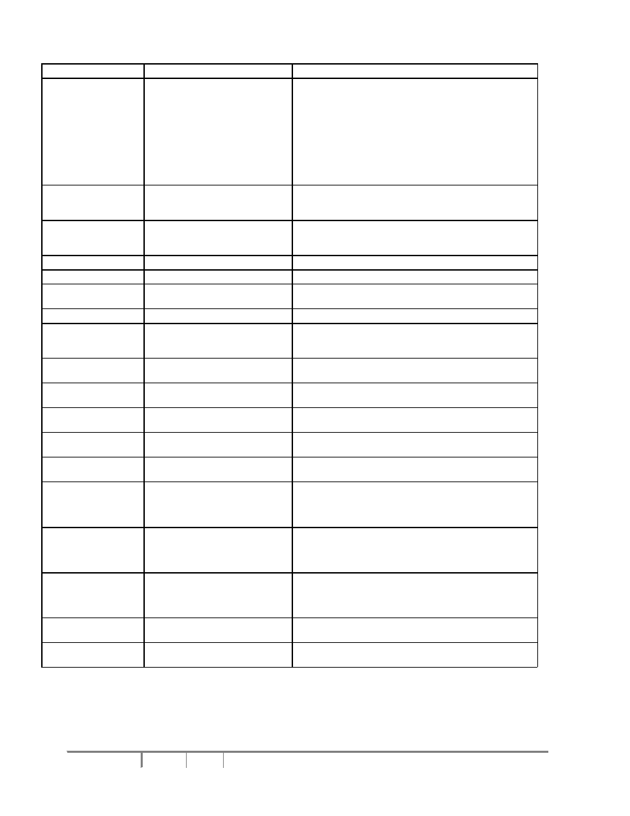
Figure 2 : Timing Characteristics for 6800-Series Parallel Interface
Symbol
Parameter
Min
Typ
Max
Unit
t
cycle
Enable Cycle Time
1000
-
-
ns
t
EH
Enable Pulse Width
-
500
-
ns
t
AS
Address Setup Time
-
200
-
ns
t
AH
Address Hold Time
-
250
-
ns
t
DS
Data Setup Time for Write Cycle
-
350
-
ns
t
DHW
Data Hold Time for Write Cycle
-
250
-
ns
t
DD
Data Delay Time for Read Cycle
-
350
-
ns
t
DHR
Data Hold Time for Read Cycle
-
100
-
ns
CLK
R/W
D/C
D
0
-D
7
(Write Cycle)
D
0
-D
7
(Read Cycle)
CE
t
AS
t
cycle
t
EH
t
DS
t
DD
t
DHW
t
DHR
t
AH
Table 1 : Timing Characteristics for 6800-Series Parallel Interface (T
A
=-30 to 85
o
C, DV
DD
=2.2 to 3.5V, V
SS
=0V)

Solomon Systech
Mar 2002
Rev 1.3
SSD1809
P 9/27
P 9/27
P 9/27
P 9/27
P 9/27
P 9/27
P 9/27
P 9/27
P 9/27
P 9/27
P 9/27
P 9/27
RD (Read Cycle)
D/C
D
0
-D
7
(Write Cycle)
D
0
-D
7
(Read Cycle)
CE
t
AS
t
cycle
t
EH
t
DS
t
D D
t
DHW
t
DHR
t
AH
WR (Write Cycle)
Symbol
Parameter
Min
Typ
Max
Unit
t
cycle
Enable Cycle Time
1000
-
-
ns
t
EH
Enable Pulse Width
-
500
-
ns
t
AS
Address Setup Time
-
200
-
ns
t
AH
Address Hold Time
-
250
-
ns
t
DS
Data Setup Time for Write Cycle
-
350
-
ns
t
DHW
Data Hold Time for Write Cycle
-
250
-
ns
t
DD
Data Delay Time for Read Cycle
-
350
-
ns
t
DHR
Data Hold Time for Read Cycle
-
100
-
ns
Table 2 : Timing Characteristics for 80-Series Parallel Interface (T
A
=-30 to 85
o
C, DV
DD
=2.2 to 3.5V, V
SS
=0V)
Figure 3 : Timing Characteristics for 80-Series Parallel Interface
Note: In Read Cycle, the WR pin should be High. In Write Cycle, the RD pin should be High.

SSD1809
Rev 1.3
Mar 2002
Solomon Systech
P 10/27
MSB IN
BIT 6..1
LSB IN
SCK
D/C
SDA
CE
t
cycle
t
D S
t
D H
t
AS
t
AH
t
EH
t
LEAD
t
LAG
Symbol
Parameter
Min
Typ
Max
Unit
t
cycle
Enable Cycle Time
1000
-
-
ns
t
EH
Enable Pulse Width
-
500
-
ns
t
AS
Address Setup Time
-
200
-
ns
t
AH
Address Hold Time
-
250
-
ns
t
DS
Data Setup Time
-
350
-
ns
t
DH
Data Hold Time
-
250
-
ns
t
LEAD
Enable Lead Time
-
350
-
ns
t
LAG
Enable Lag Time
-
100
-
ns
Table 3 : Timing Characteristics for Serial Peripheral Interface (SPI) (T
A
=-30 to 85
o
C, DV
DD
=2.2 to 3.5V, V
SS
=0V)
Figure 4 : Timing Characteristics for Serial Peripheral Interface (SPI)

Solomon Systech
Mar 2002
Rev 1.3
SSD1809
P 11/27
P 11/27
P 11/27
P 11/27
P 11/27
P 11/27
P 11/27
P 11/27
P 11/27
P 11/27
P 11/27
P 11/27
P/S (Parallel / Serial Interface)
This pin is an input pin which is used to select parallel interface or
serial interface. Input High for parallel interface (6800 or 80) while input
Low for serial interface (SPI).
68/80
This pin is an input pin which is used to select 6800 interface or 80
interface. Input High for 6800 interface while input Low for 80 interface.
D/C (Data / Command)
This input pin acknowledges the LCD driver that the input at SDA/D
0
-
D
7
is data or command. Input High for data while input Low for com-
mand.
CE (Chip Enable)
This pin is an input pin. The chip is enabled when this pin is Low.
CLK/ WR / SCK
When 6800-series parallel interface is selected, this input pin is
named as CLK which is a clock. Data on SDA/D
0
-D
7
are latched at the
falling edge of CLK.
When 80-series parallel interface is selected, this input pin is named
as WR which is a clock in write cycle. It is low enable for write data/
command and data on SDA/D
0
-D
7
are latched at the rising edge of WR.
In read cycle, this pin should be High.
When SPI is selected, this input pin is named as SCK which is a
serial clock. Data on SDA /D
0
is latched at the falling edge of SCK.
RES (Reset)
An active Low pulse to this pin reset the internal status of the driver
(same as power on reset). The minimum pulse width is 1
µ
s to initiate
the reset process.
SDA / D
0
-D
7
(Data)
SDA/D
o
-D
7
is a bi-directional bus and is used for data/command
transfer. If 6800-series or 80-series parallel interface is selected, D
0
-D
7
are connected directly to MCU for data transfer.
When SPI is selected, D
0
is named as SDA which is a serial input of
the driver. It receives data/command from MCU to driver and transfers
serially. Meanwhile, D
1
-D
7
pins can be High or Low.
R/W / RD
When 6800-series parallel interface is selected, this input pin is
named as R/W, Input High will read the display data RAM or the internal
status (Busy/Idle) while input Low will write the display data RAM or the
internal setup registers.
When 80-series parallel interface is selected, this input pin is named
as RD and is a clock in read cycle. It is low enable for read data/com-
mand and data SDA/D
0
-D
7
are latched at the rising edge of RD. In write
cycle, this pin should be High.
When SPI is selected, this input pin can be High or Low.
OSC1 (Oscillator Input)
For internal oscillator mode, this is an input pin for the internal low
power RC oscillator circuit. In this mode, an external resistor of certain
value should be connected between the OSC1 and OSC2 pins for a
range of internal operating frequencies (refer to Figure 1). For external
oscillator mode, OSC1 should be left open.
OSC2 (Oscillator Output / External Oscillator Input)
For internal oscillator mode, this is an output for the internal low
power RC oscillator circuit. For external oscillator mode, OSC2 will be
an input pin for external clock and no external resistor is needed.
V
L L 6
- V
LL2
Group of voltage level pins for driving the LCD panel. They can either
be connected to external driving circuit for external bias supply or con-
nected internally to built-in divider circuit if internal divider is enable. For
internal Voltage Generator enabled, a 1.0
µ
F capacitor to AV
SS
is
required on each pin.
DUM1 - DUM4
If the internal bias voltage levels generator is enabled, a 1
µ
F
capacitor to AV
SS
is required on each pin.
C
1N
and C
1P
, C
2N
and C
2P
, C
3N
and C
3P
If internal Voltage Generator is enabled with 2X DC-DC converter, a
0.1
µ
F capacitor is required to connect between C
1N
& C
1P
.
If internal Voltage Generator is enabled with 3X/4X DC-DC con-
verter, a 0.1
µ
F capacitor is required to connect between C
1N
& C
1P
and
C
3N
& C
3P
.
If internal Voltage Generator is enabled with 5X DC-DC converter, a
0.1
µ
F capacitor is required to connect these three pair of pins.
C+ and C-
If internal divider circuit is enabled, a 1
µ
F capacitor is required to
connect between these two pins.
V
R
and V
F
This is a feedback path for the gain control (external contrast control)
of V
LL2
to V
LL6
. For adjusting the LCD driving voltage, it requires a feed-
back resistor placed between V
R
and V
F
, a gain control resistor placed
between V
F
and AV
SS
, a 4.7
µ
F capacitor placed between V
R
and
AV
SS
. (Refer to the Application Circuit)
COM0-COM64 (Row Drivers)
These lines provide the LCD row driving signals to the LCD panel.
COM64 also serves as the common driving signal in the icon mode.
Output is 0V during display off.
SEG0-SEG159 (Column Drivers)
These 160 pins provide LCD column driving signal to LCD panel.
Output is 0V during display off.
AV
DD
and AV
SS
AV
DD
and AV
SS
are the positive supply and ground to all of the ana-
log circuit respectively.
V
CC
For using the internal Voltage Generator, a 0.1
µ
F capacitor from this
pin to AV
SS
is required. It can also be an external bias input pin if inter-
nal Voltage Generator is not used. Power is supplied to the LCD Driving
Level Selector and HV Buffer Cell with this pin. Normally, this pin is not
intended to be a power supply to other components.
DV
DD
and DV
SS
Power is supplied to the digital control circuit and DC/DC converter of
the driver using these two pins. DV
DD
is power and DV
SS
is ground.
V
DC
V
DC
is the power supply to the DC/DC converter of the driver.
Remark: In SSD1809T TAB package, V
DC
pin is connected to DV
DD
and P/S pin & 68/80 pin are connected to AV
DD
. Only 6800-parallel
interface can be used and DV
DD
will be the supply of the DC/DC con-
verter in this package.
PIN DESCRIPTIONS

SSD1809
Rev 1.3
Mar 2002
Solomon Systech
P 12/27
OPERATION OF LIQUID CRYSTAL DISPLAY DRIVER
Description of Block Diagram Module
Command Decoder and Command Interface
This module determines whether the input data is interpreted as
data or command. Data is directed to this module based upon the
input of the D/ C pin. If D/C is high, data is written to Graphic Display
Data RAM (GDDRAM). If D/C is low, the input at SDA/D
0
-D
7
is inter-
preted as a Command and it will be decoded and written to the corre-
sponding command register.
Reset is of the same function as Power ON Reset (POR). Once
RES receives a negative reset pulse of minimium 1
µ
s, all internal cir-
cuit will be back to its initial status.
MPU 6800-series Parallel Interface
The parallel interface consists of 8 bi-directional data pins (D
0
-D
7
),
R/W, D/C, CE, and CLK. R/W input High indicates a read operation
from the Graphic Display Data RAM (GDDRAM) or the status regis-
ter.R/W input Low indicates a write operation to Display Data RAM or
Internal Command Registers depending on the status of D/C input.
The chip is enabled when the CE is low and the CLK input serves as
data latch signal (clock). Refer to Figure 2 showing timing character-
istics for 6800-series parallel interface.
MPU 80-Series Parallel Interface
The parallel interface consists of 8 bi-directional data pins (D
0
-D
7
),
RD, WR, D/C, and CE . RD input serves as data read latch signal
(clock) provided that CE is low. WR input serves as data write latch
signal(clock) provided that CE is low. Whether it is display data or
command register write is controlled by D/C. Refer to Figure 3 show-
ing timing characteristics for 80-series parallel interface.
LSB
MSB
Column address 00H
(or column address 9FH)
Column address 9FH
(or column address 00H)
Page 1
COM0
(COM63)
COM63
(COM0)
S
E
G
0
S
E
G
1
5
9
Row 0
Note : The configuration in parentheses represent the remapping of Rows and Columns
LSB
Row 64 Page 9
COM64
Row 63
Figure 5 : Graphic Display Data RAM (GDDRAM) Address Map
LSB
MSB
LSB
MSB
Page 2
Page 8
MPU Serial Peripheral Interface
The serial interface consists of serial clock SCK, serial data SDA,
D/C, and CE. The chip is enabled when CE is low and SDA is shifted
into a 8-bit shift register on every falling edge of SCK and data are
transferred serially with MSB first and LSB last. D/C is sampled on
every first clock of each byte cycle and the information is interpreted
as Display Data or Command accordingly.
The eight bits information from SDA pin are stored in a buffer shift
register. After the next byte information from SDA pin is written into
the buffer, the original contents in the buffer will be sent to Display
Data RAM or Command Register. A No-Operation (01101000 ) com-
mand could be written to push the last information in the buffer into
Display RAM or Command Register.
The first bit after the CE pin falling edge or the RES pin rising edge
is always interpreted as MSB.
Refer to Figure 4 showing timing characteristics for Serial Periph-
eral Interface.
Selection of Interface
Selection of the desired interface is done by putting P/S and 68/80
either high or low as shown in the following table:-
PIN
6800-Series
80-Series
SPI
P/S
High
High
Low
68/80
High
Low
High/Low

Solomon Systech
Mar 2002
Rev 1.3
SSD1809
P 13/27
P 13/27
P 13/27
P 13/27
P 13/27
P 13/27
P 13/27
P 13/27
P 13/27
P 13/27
P 13/27
P 13/27
Graphic Display Data RAM (GDDRAM)
The GDDRAM is a bit mapped static RAM holding the bit pattern
to be displayed. The size of the RAM is determined by number of
row times the number of column (160x65 = 10400 bits). Figure 5 is a
description of the GDDRAM address map. For mechanical flexibility,
re-mapping on both Segment and Common outputs are provided.
Figure 6 : Oscillator Circuitry
Oscillation Circuit
enable2
OSC1
OSC2
Feedback for internal oscillator
For external CLK input
Oscillator enable
SSD1809
External component
Buffer
enable1
enable
Internal Oscillator selected
LCD Driving Voltage Generator and Regulator
This module generates the LCD voltage needed for display output.
It takes a single supply input and generate necessary bias voltages.
It consists of :
1. 2X, 3X, 4X and 5X DC-DC Converter
To generate the V
CC
voltage. 2X, 3X and 4X DC-DC converter are
used for LCD panel which needs lower driving voltage for less
power consumption. 5X DC-DC converter is used for LCD panel
which needs higher driving voltage.
2. Voltage Regulator
Feedback gain control for initial LCD voltage. it can also be used
with external contrast control.
3. Voltage Divider
Divide the LCD display voltage (V
LL2
-V
LL6
) from the regulator out-
put. This is a low power consumption circuit which can save the
most display current compare with traditional resistor ladder
method.
4. Self adjust temperature compensation circuitry
Provide 2 different compensation grade selections to satisfy the
various liquid crystal temperature grades. The grading can be
selected by software control.
5. Contrast Control Block
Software control of 16 voltage levels of LCD voltage.
All blocks can be individually turned off if external voltage genera-
tor is employed.
Figure 7a : LCD Display Example "0"
COM1
COM2
COM3
COM4
COM5
COM6
COM7
S
E
G
1
S
E
G
2
S
E
G
3
S
E
G
4
COM0
S
E
G
0
65 Bit Latch / 160 Bit Latch
A 225 bit long register which carries the display signal information.
First 65 bits are Common driving signals and other 160 bits are Seg-
ment driving signals. Data will be input to the HV-buffer Cell for
bumping up to the required level.
Level Selector
Level Selector is a control of the display synchronization. Display
voltage can be separated into two sets and used with different
cycles. Synchronization is important since it selects the required LCD
voltage level to the HV Buffer Cell for output signal voltage pump.
HV Buffer Cell (Level Shifter)
HV Buffer Cell works as a level shifter which translates the low
voltage output signal to the required driving voltage. The output is
shifted out with an internal FRM clock which comes from the Display
Timing Generator. The voltage levels are given by the level selector
which is synchronized with the internal M signal.
Display Timing Generator
This module is an on chip low power RC oscillator circuitry (Fig-
ure 6). The oscillator frequency can be selected in the range of
25kHz to 200kHz by external resistor. One can enable the circuitry
by software command. For external clock provided, feed the clock to
OSC2 and leave OSC1 open.

SSD1809
Rev 1.3
Mar 2002
Solomon Systech
P 14/27
V
LL6
V
LL5
V
LL4
V
LL3
V
LL2
V
SS
-V
LL2
-V
LL3
-V
LL4
-V
LL5
-V
LL6
SEG0-COM0
Non-selected
Pixel
SEG0-COM1
Selected
Pixel
1 2 3 4
1 2 3 4
TIME SLOT
V
LL6
V
LL5
V
LL4
V
LL3
V
LL2
V
SS
-V
LL2
-V
LL3
-V
LL4
-V
LL5
-V
LL6
1 2 3 4
1 2 3 4
V
LL6
V
LL5
V
LL4
V
LL3
V
LL2
V
SS
COM0
COM1
SEG0
SEG1
TIME SLOT
V
LL6
V
LL5
V
LL4
V
LL3
V
LL2
V
SS
V
LL6
V
LL5
V
LL4
V
LL3
V
LL2
V
SS
V
LL6
V
LL5
V
LL4
V
LL3
V
LL2
V
SS
Figure 7b : LCD Driving Signal from SSD1809
Figure 7c : Effective LCD waveform on LCD pixel
M

Solomon Systech
Mar 2002
Rev 1.3
SSD1809
P 15/27
P 15/27
P 15/27
P 15/27
P 15/27
P 15/27
P 15/27
P 15/27
P 15/27
P 15/27
P 15/27
P 15/27
Command Description
Display On (Display Mode)
This command turns the LCD Common and Segment outputs on.
This command starts the conversion of data in GDDRAM to necessary
waveforms on the Common and Segment driving outputs. The on-chip
bias generator is also turned on by this command. (Note : "Oscillator
On" command should be sent before "Display On" is selected)
Display Off (Stand-by Mode)
This command turns the display off and the states of the LCD driver
are as follow during display off :
1. The Common and Segment outputs are fixed at V
SS
.
2. The Bias Voltage Generator is turned off.
3. The RAM and content of all registers are retained.
4. IC will accept new commands and data.
The Oscillator is not affected by this command.
Set GDDRAM Column Address
This command positions the address pointer on a column location.
The address can be set to location 00H-9FH (160 columns) and the
MSB is software set by "set MSB of GDDRAM Column Address" . The
column address will be increased automatically after a read or write
operation. Refer to "Address Increment Table" and command "Set
GDDRAM Page Address" for further information.
Set GDDRAM Page Address
This command positions the row address to 1 of 9 possible positions
in GDDRAM. Refer to figure 5.
Save / Restore Column Address
Save Column Address command saves a copy of the Column
Address of GDDRAM. Restore Column Address command restores the
copy obtained from the previous execution of saving column address.
This instruction is very useful for writing full graphics characters that are
larger than 8 pixels vertically.
Master Clear GDDRAM
This command is to clear the content of the Display Data RAM to
zero. Issue this command followed by a dummy write data.
Master Clear Icon RAM
This command is used to clear the content of the Icon Data RAM to
zero. Set the page pointer to icon page (page 9) and then issue this
command followed by a dummy write data.
Set Page Mask
This command is used to define the page which will be masked.
Once the command "Set Page Mask" is issued, the next command will
be written to the Page Mask Register which is an 8-bit register. Each bit
represents one of the 8 pages: page mask bit 0 represents Page 1,
page mask bit 1 represents Page 2, ... etc.
Enable Page Mask
When the Page Mask is enabled, the display of those pages, with
page mask bit set, will be cleared. Meanwhile, the data in the display
RAM is retained.
Enable Icon Mask
When the Icon Mask is enabled, the display of the icons will be
cleared. Meanwhile, the data in the icon display RAM is retained.
Set Logical Page Mask
This command is used to select the page mask type. There are two
page mask types 1) Physical page mask and 2)Logical page mask.
Physical mask refers to a physical location of the panel which cannot be
moved by scrolling, row remap or panel offset. Logical page mask
refers to the location of GDDRAM. Therefore a logical mask will keep
masking a definite area of GDDRAM content when the contain is
moved along the panel by scrolling, row remap or panel offset.
Set Display Mode
This command switches the driver to full display mode or icon display
mode. In low power icon mode, only icons (driven by COM64) are dis-
played. The DC-DC converter, the voltage generator and the regulator
are disabled. All V
CC
, V
LL
s pins cannot have external bias voltage sup-
ply in the low power icon mode. Refer "Set Icon Mode" for further infor-
mation.
Set Icon Mode
This command is used to select one of 4 smart icon modes.
In smart icon mode A, on-pixels are stressed by a voltage with root-
mean-square value of 1xV
DD
whereas off-pixels by 0.58xV
DD
.
In smart icon mode B, on-pixels are stressed by a voltage with root-
mean-square value of 0.87xV
DD
whereas off-pixels by 0.5xV
DD
.
In smart icon mode C, on-pixels are stressed by a voltage with root-
mean-square value of 0.71xV
DD
whereas off-pixels by 0.41xV
DD
.
In smart icon mode D, on-pixels are stressed by a voltage with root-
mean-square value of 0.58xV
DD
whereas off-pixels by 0.33xV
DD
.
Remark: Icon Mode cannot be used if external divider is used.
Set Display Frequency
In half display frequency mode, the display frame frequency will be
halved. Also, the operation frequency of analog circuitries will be halved
as well.
Set Frame Frequency
This command is used to select one of 16 frame frequencies from
Fosc/(2 x Mux Ratio) to Fosc/(32 x Mux Ratio). When the "Frame Fre-
quency " command is issued, the following command will be written to
the "Frame Frequency Register" which is used to define the desired
frame frequencies.
Set Bias Ratio
This command sets the bias of 1:5, 1:7, 1:8 or 1:9 bias for the divider
output. The selection should match the characteristic of LCD Panel.
Oscillator Enable
This command is used to either turn on / off Oscillator. For using
internal or external oscillator, this command should be executed. The
setting for this command is not affected by command "Set Display On/
Off". See command "Ext/Int Oscillator" for more information
Ext / Int Oscillator
This command is used to select either internal or external oscillator.
When internal oscillator is selected, feedback resistor between OSC1
and OSC2 is needed. For external oscillation circuit, feed clock input
signal to OSC2 and leave OSC1 open.
Voltage Generator Enable
This command is used to enable the internal Voltage Generator to
generate the V
CC
from AV
DD
. Disable the voltage generator if external

SSD1809
Rev 1.3
Mar 2002
Solomon Systech
P 16/27
Vcc is provided.
Set 2X / 3X / 4X / 5X Converter
This command selects the usage of 2X / 3X / 4X / 5X Converter
when the internal voltage Generator is enabled.
Set DC/DC Converter Mode
This command sets the DC/DC converter to regulated mode. In regu-
lated mode, V
CC
voltage equals to V
R
voltage.
Voltage Regulator Enable
This command enables regulator which consists of the internal con-
trast control and temperature compensation circuits.
Internal Voltage Divider Enable
If the internal divider is disabled, external bias can be used for V
LL6
to V
LL2.
If the internal divider is enabled, the internal circuit will gener-
ated the 1:5 / 1:7 / 1:8 / 1:9 bias driving voltage.
Internal Contrast Control Enable
This command is used to adjust the delta voltage of the bias volt-
ages. With bit option = 1, the software selection for delta bias voltage
control is enabled. With bit option = 0, internal contrast control is dis-
abled.
Increase / Decrease Contrast Level
If the internal contrast control is enabled, this command is used to
increase or decrease the contrast level within the 16 contrast levels.
Set Contrast Level
This command is used to select one of the 16 contrast levels from
10h to 1Fh when internal contrast control circuitry is in use.
Set Temperature Coefficient
This command can select 2 different LCD driving voltage tempera-
ture coefficients to match various liquid crystal temperature grades.
Those temperature coefficients are specified in Electrical Characteris-
tics Tables.
Set MUX Ratio / Chinese Character Mode (Partial Display)
This command is used to select the Graphic display mode with differ-
ent Mux from 2 Mux to 65 Mux or the Chinese character display mode
with different character line from 1 line to 3 lines. Figure 8a & 8b in the
section "Display Output Description" show the 65 Mux Graphic display
mode and 3-line Chinese character display mode respectively.
Set Row Re-Mapping
This instruction selects the mapping of Display Data RAM to Com-
mon drivers for mechanical flexibility. There are 2 mappings:
1. Row(0) - Row(Mux ratio-2) of GDDRAM mapped to COM(first dis-
play row location) - COM( first display row location+Mux ratio-2). Exam-
ple is illustrated in figure 8b, the first display row location is COM0 and
the Mux ratio is 53, then Row0 of GDDRAM wil be mapped to COM0,
Row1 through Row 51 of GDDRAM will be mapped to COM1 to
COM51.
2. Row(0) - Row(Mux ratio-2) of GDDRAM mapped to COM(first dis-
play row location+Mux ratio-2) - COM(first display row location). Exam-
ple is illustrated in figure 8c, Row0 - Row51 of GDDRAM is mapped to
COM51 - COM0.
Set Column Re-Mapping
This instruction selects the mapping of new Display Data RAM to
Segment drivers for mechanical flexibility. There are 2 mappings to
select:
1. Column 0 - Column 159 of GDDRAM mapped to SEG0-SEG159
respectively;
2. Column 0 - Column 159 of GDDRAM mapped to SEG159-SEG0
respectively.
Detailed information please refer to Figure 8d in the section "Display
Output Description".
Set Vertical Scroll Value
In Graphic display mode, this command maps the selected
GDDRAM rows (00H-3FH) to COM pins. With scroll value equals to 0,
Row 0 of GDDRAM is mapped to COM0 and Row 1 through Row 63
are mapped to COM1 through COM63 respectively. With scroll value
equal to 1, Row 1 of GDDRAM is mapped to COM0, then Row 2
through Row 63 will be mapped to COM1 through COM62 respectively
and Row 0 will be mapped to COM63.
In Chinese character display mode, there are 73 rows of display con-
tent including space and icon. This command moves the display con-
tent downward equals to the value stored vertical scrolling register.
Set Display Rows Location
This command is used to define the first row location of the display,
the first row can be started at COM0 to COM63. Example is given in
Figure 8h.

Solomon Systech
Mar 2002
Rev 1.3
SSD1809
P 17/27
P 17/27
P 17/27
P 17/27
P 17/27
P 17/27
P 17/27
P 17/27
P 17/27
P 17/27
P 17/27
P 17/27
Figure 8a: Content in GDDRAM
Figure 8c: Row remap enable
Figure 8d: Column remap enable & Re-write RAM content
Display Output Description
This is an example of output pattern on the LCD panel. Figure 8a
shows the content in GDDRAM and Figure 8b - 8h illustrate the output
patterns on the LCD display with a sequence of commands:
1) Set 3-line Chinese character display mode shown in Figure 8b,
2) Enable row re-mapping shown in Figure 8c,
3) Enable column re-mapping & rewrite RAM content shown in Figure 8d,
4) Enable vertical scrolling command with scrolling value of 07h shown in
Figure 8e,
5) Disable row re-mapping & column re-mapping and rewrite map content
shown in Figure 8f,
6) Enable vertical scrolling command with scrolling value of 3Eh shown in
Figure 8g and
7) Set display rows location at 06h shown in Figure 8h.
Figure 8e: Vertical scrolling with writing 07h to scrolling register
Figure 8f: Disable row re-mapping & column re-mapping and
Figure 8g: Vertical scrolling with writing 3Eh to scrolling register
Figure 8h: Centering with display rows locatiion 06h
Figure 8b: 3-line Chinese character mode
Rewrite map content.
SSD1809
Rev 1.3
Mar 2002
Solomon Systech
P 18/27
COMMAND TABLE
Bit Pattern
Command
Comment
0000X
3
X
2
X
1
X
0
Set GDDRAM Page Address
Set GDDRAM Page Address using X
3
X
2
X
1
X
0
as address bits.
X
3
X
2
X
1
X
0
=0000 : page 1 (POR)
X
3
X
2
X
1
X
0
=0001 : page 2
X
3
X
2
X
1
X
0
=0010 : page 3
X
3
X
2
X
1
X
0
=0011 : page 4
X
3
X
2
X
1
X
0
=0100 : page 5
X
3
X
2
X
1
X
0
=0101 : page 6
X
3
X
2
X
1
X
0
=0110 : page 7
X
3
X
2
X
1
X
0
=0111 : page 8
X
3
X
2
X
1
X
0
=1000 : page 9
00001001
Set Display Rows Location
Next Command (byte) on D
5
~ D
0
defines the display rows loca-
tion.
Starts at Row0 - COM0 (POR)
0000101X
0
Set 2X/3X DC-DC Converter
X
0
=0 : Enable 2X Converter
X
0
=1 : Enable 3X Converter
Remark: This command overrides "Set 4X/5X DC-DC Converter".
000011 X
1
X
0
Reserved
00001110
Reserved
0001X
3
X
2
X
1
X
0
Set Contrast Level
Set one of the 16 contrast level values using X
3
X
2
X
1
X
0
as data
bits. Reset to 0000 during POR.
00001111
Reserved
0010000X
0
Set 4X / 5X DC-DC Converter
X
0
=0: Enable 4X Converter (POR)
X
0
=1: Enable 5X Converter
Remark: This command overrides "Set 2X/3X DC-DC Converter".
0010001X
0
Set Segment Re-Mapping
X
0
=0 : Column 0 to SEG0 (POR)
X
0
=1 : Column 0 to SEG159
0010010X
0
Set Common Re-Mapping
X
0
=0 : Row 0 to Display Row location (POR)
X
0
=1: Flip the Row-COM mapping.
0010011X
0
Set MSB of GDDRAM Column
Address
X
0
=0: MSB = 0 (POR)
X
0
=1: MSB = 1
0010100X
0
Set Display on/off
X
0
=0: Display off (POR)
X
0
=1: Display on
0010101X
0
Voltage Generator Enable
X
0
=0: Disable Voltage Generator (POR)
X
0
=1: Enable Voltage Generator
0010110X
0
Voltage Regulator Enable
X
0
=0: Disable Regulator (POR)
X
0
=1: Enable Regulator
When application uses a supply with built-in temperature compen-
sation, the regulator should be disabled.
0010111X
0
Voltage Divider Enable
X
0
=0: Disable Voltage Divider (POR)
X
0
=1: Enable Voltage Divider
When an external bias network is preferred, the voltage divider
should be disabled.
0011000X
0
Internal Contrast Control Enable
X
0
=0: Disable Internal Contrast Control(POR)
X
0
=1: Enable Internal Contrast Control
Internal contrast circuits can be disabled if external contrast cir-
cuits is preferred.
0011001X
0
Set Display Frequency
X
0
=0 : Normal display frequency (POR)
X
0
=1 : Half display frequency
0011010X
0
Save/Restore GDDRAM Column
Address
X
0
=0 : Restore address
X
0
=1 : Save address
Solomon Systech
Mar 2002
Rev 1.3
SSD1809
P 19/27
P 19/27
P 19/27
P 19/27
P 19/27
P 19/27
P 19/27
P 19/27
P 19/27
P 19/27
P 19/27
P 19/27
Bit Pattern
Command
Comment
00110110
Master Clear GDDRAM
Master clear GDDRAM (160 X 64 bits)
00110111
Master Clear Icons RAM
Master Clear of Icons RAM
0011100X
0
Set Bias Ratio 1:9 or 1:7
X
0
=0 : bias = 1 : 9 (POR)
X
0
=1 : bias = 1 : 7
Remark: This command overrides "Set Bias 1:8 or 1:5".
0011101X
0
Reserved
0011110X
0
Set Bias Ratio 1:8 or 1:5
X
0
=0 : bias = 1 : 8
X
0
=1 : bias = 1 : 5
Remark: This command overrides "Set Bias 1:9 or 1:7".
0011111X
0
Set Display Mode
X
0
=0 : Low power icon display mode
X
0
=1 : Normal display mode (POR)
01000000
Set Vertical Scroll
Next command will be written to vertical scroll register.
Scroll register=0 upon POR
01000001
Set Page Mask
Next command (byte) will be written to page mask register.
Page mask register=0 upon POR
0100001X
0
Set Logical Page Mask
X
0
=0 : Enable Physical Page Mask (POR)
X
0
=1 : Enable Logical Page Mask
0100010X
0
Enable Page Mask
X
0
=0 : Disable page mask (POR)
X
0
=1 : Enable page mask
0100011X
0
Enable Icon Mask
X
0
=0 : Disable icon mask (POR)
X
0
=1 : Enable icon mask
010010X
1
X
0
Reserved
010011X
1
X
0
Reserved
0101X
3
X
2
X
1
X
0
Reserved
011000X
1
X
0
Reserved
011001X
1
X
0
Set Icon Mode
X
1
X
0
=00 : Icon Mode A
X
1
X
0
=01 : Icon Mode B
X
1
X
0
=10 : Icon Mode C (POR)
X
1
X
0
=11 : Icon Mode D
Remark: Icon Mode cannot be used if external divider is used.
0110100X
0
No operation
01101010
Set Mux Ratio / Chinese Character
Mode
Next command (byte) on D
7
~D
0
defines the size of panel.
D
7
=0 : Graphic Mode
D
5
D
4
D
3
D
2
D
1
D
0
= 000000 : 1 graphic row (2 Mux)
D
5
D
4
D
3
D
2
D
1
D
0
= 000001 : 2 graphic rows (3 Mux)
D
5
D
4
D
3
D
2
D
1
D
0
= 000010 : 3 graphic rows (4 Mux)
:
:
:
D
5
D
4
D
3
D
2
D
1
D
0
= 111110 : 63 graphic rows (64 Mux)
D
5
D
4
D
3
D
2
D
1
D
0
= 111111 : 64 graphic rows (65 Mux) (POR)
*D
6
: Don't care.
D
7
= 1 : 16-Point Chinese Character Mode
D
1
D
0
= 00 - 1 character row (17 Mux)
D
1
D
0
= 01 - 2 character rows (35 Mux)
D
1
D
0
= 10 - 3 character rows (53 Mux)
*D
6
~D
2
: Don't care.

SSD1809
Rev 1.3
Mar 2002
Solomon Systech
P 20/27
Bit Pattern
Command
Comment
01101011
Set Frame Frequency
Next command (byte) on D
3
~D
0
will be written to the Frame Fre-
quency Register.
D
3
D
2
D
1
D
0
= 0000 : Frame Frequency Register = 0
D
3
D
2
D
1
D
0
= 0001 : Frame Frequency Register = 1
D
3
D
2
D
1
D
0
= 0010 : Frame Frequency Register = 2
:
:
:
D
3
D
2
D
1
D
0
= 0101 : Frame Frequency Register = 5 (POR)
:
:
:
D
3
D
2
D
1
D
0
= 1111 : Frame Frequency Register = 15
*D
7
~D
4
: Don't care.
011011X
1
X
0
Set Temperature Coefficient
X
1
X
0
=00: 0.00% (POR)
X
1
X
0
=11: -0.35%
0111000X
0
Increase/Decrease Contrast Value
X
0
=0: Decrease by one level
X
0
=1: Increase by one level
0111001X
0
Reserved
0111010X
0
Set DC-DC Converter Mode
X
0
=0 : Normal Mode (POR)
X
0
=1 : Regulated Mode
0111011X
0
Reserved
01111000
Reserved
01111001
Reserved
0111101X
0
Set External / Internal Oscillator
X
0
=0: Internal Oscillator (POR)
X
0
=1: External Oscillator
For internal oscillator mode, place a resistor between OSC1 and
OSC2 pins. For external oscillator mode, feed clock input to OSC2
pin.
0111110X
0
Reserved
0111111X
0
Set Oscillator Enable
X
0
=0: Oscillator Master Disable(POR)
X
0
=1: Oscillator Master Enable
This is the master control for oscillator circuitry. This command
should be issued after the "External/Internal Oscillator" command.
1X
6
X
5
X
4
X
3
X
2
X
1
X
0
Set GDDRAM Column Address
Set GDDRAM Column Address.Use X
6
X
5
X
4
X
3
X
2
X
1
X
0
as address
bits. MSB of the address set by "Set MSB of GDDRAM column
address command.

Solomon Systech
Mar 2002
Rev 1.3
SSD1809
P 21/27
P 21/27
P 21/27
P 21/27
P 21/27
P 21/27
P 21/27
P 21/27
P 21/27
P 21/27
P 21/27
P 21/27
Data Read / Write
6800-Series Parallel Interface
To read data from the GDDRAM, input High to R/W pin and D/ C pin. Data are valid at the falling edge of CLK. And the GDDRAM column
address pointer will be increased by one automatically.
To write data to the GDDRAM, input Low to R/W pin and High to D/ C pin. Data which fulfil the data setup time, are input to the LCD driver at
the falling edge of CLK. And the GDDRAM column address pointer will be increased by one automatically.
80-Series Parallel Interface
To read data from the GDDRAM, input High to WR pin and D/C pin and RD is used as a clock input. Data are valid at the rising edge of RD.
And the GDDRAM column address pointer will be increased by one automatically.
To write data to the GDDRAM, input High to RD pin and D/C pin and WR pin is used as a clock input. Data which fulfil the data setup time,
are input to the LCD driver at the rising edge of WR. And the GDDRAM column address pointer will be increased by one automatically.
SPI Interface
Input High to D/C pin to write data to the GDDRAM. Data which fulfil the data setup time, are input to the LCD driver at the falling edge of
SCK. And the GDDRAM column address pointer will be increased by one automatically.
Read data from GDDRAM is not available.
No auto address pointer increment will be performed for the Dummy Write Data after Master Clear GDDRAM. (Refer to the "Commands
Required for R/W Actions on RAM" Table)
Comment
Address Increment
Remarks
Write Command
No
Read Command
No (invalid mode)
*1
Write Data
Yes
*2, *3
Read Data
Yes
*3
Commands Required for R/W Actions on RAM
* No need to resend the command again if it is set previously.
The read / write action to the Display Data RAM does not depend on the display mode. This means the user can change the RAM content
whether the target RAM content is being displayed.
R/W Actions on RAMs
Commands Required
Read/Write Data from/to GDDRAM.
Set GDDRAM Page Address
Set MSB of GDDRAM Column Address
Set GDDRAM Column Address
Read/Write Data
(000000X
1
X
0
)*
(0010011X
0
)*
(1X
6
X
5
X
4
X
3
X
2
X
1
X
0
)*
(X
7
X
6
X
5
X
4
X
3
X
2
X
1
X
0
)
Save/Restore GDDRAM Column Address.
Save/Restore GDDRAM Column Address.
(0011010X
0
)
Master Clear GDDRAM
Set Clear Page GDDRAM (160 x 64 bits)
Dummy Write Data
(00110110)
(X
7
X
6
X
5
X
4
X
3
X
2
X
1
X
0
)
Master Clear Icon RAM
Set GDDRAM Page Address to Page 9
Master Clear Icon RAM (160 bits)
Dummy Write Data
(00001001)*
(00110111)
(X
7
X
6
X
5
X
4
X
3
X
2
X
1
X
0
)
Address Increment is done automatically data read write. The column address pointer of GDDRAM
*3
is affected.
Remarks :
*1. Only data is read from RAM.
*2. If write data is issued after Command Clear RAM, Address increase is not applied.
*3. Column Address will be wrapped round when overflow.
Address Increment Table (Automatic)

SSD1809
Rev 1.3
Mar 2002
Solomon Systech
P 22/27
V
R
V
F
C
3P
C
3N
C+
C-
OSC1
OSC2
1
µ
F
R
3
900k
4.7
µ
F
2M
500k
560pF
1
µ
F
1
µ
F
1
µ
F
1
µ
F 1
µ
F
1
µ
F
To
LCD
Panel
COM0 to
COM64
SEG0 to
SEG159
V
DD
0.1
µ
F
CMOS
MPU/MCU
RAM
EPROM
RES
D/C
CLK/WR/SCK
R/W / RD
DV
DD
AV
DD
SDA/D
0
~D
7
SSD1809
AV
SS
V
LL2
V
LL3
V
LL4
V
LL5
V
LL6
V
CC
DV
SS
1
µ
F
1
µ
F
1
µ
F
0.1
µ
F
DUM1 DUM2 DUM3 DUM4
C
2P
C
2N
C
1P
C
1N
0.1
µ
F
CE
Application Circuit for 2X DC-DC converter:
(All Internal Analog Block Enabled)
Remarks :
1.
R
3
can be omitted for external oscillator.
2.
V
R
and V
F
can be left open for Regulator disable, TC = 0% and Contrast Disable.
3. RES , CLK/WR/SCK, R/ W/RD, CE and D/C should be at a known state.
P/S
68/80
Solomon Systech
Mar 2002
Rev 1.3
SSD1809
P 23/27
P 23/27
P 23/27
P 23/27
P 23/27
P 23/27
P 23/27
P 23/27
P 23/27
P 23/27
P 23/27
P 23/27
0.1
µ
F
0.1
µ
F
Application Circuit for 3X/4X DC-DC converter:
(All Internal Analog Block Enabled)
Remarks:
1.
R
3
can be omitted for external oscillator.
2.
V
R
and V
F
can be left open for Regulator disable, TC = 0% and Contrast Disable.
3. RES, CLK/WR/SCK, R/W/RD, CE and D/C should be at a known state.
V
R
V
F
C
3P
C
3N
C+
C-
OSC1
OSC2
1
µ
F
R
3
900k
4.7
µ
F
2M
500k
560pF
1
µ
F
1
µ
F
1
µ
F
1
µ
F
1
µ
F
1
µ
F
To
LCD
Panel
COM0 to
COM64
SEG0 to
SEG159
V
DD
0.1
µ
F
CMOS
MPU/MCU
RAM
EPROM
RES
D/C
CLK/ W R/SCK
R/W / RD
DV
DD
AV
DD
SDA/D
0
~D
7
SSD1809
AV
SS
V
LL2
V
LL3
V
LL4
V
LL5
V
LL6
V
CC
DV
SS
1
µ
F
1
µ
F 1
µ
F
0.1
µ
F
DUM1 DUM2 DUM3 DUM4
C
2P
C
2N
C
1P
C
1N
CE
P /S
68/80

SSD1809
Rev 1.3
Mar 2002
Solomon Systech
P 24/27
0.1
µ
F
0.1
µ
F
0.1
µ
F
Application Circuit for 5X DC-DC converter:
(All Internal Analog Block Enabled)
Remarks :
1.
R
3
can be omitted for external oscillator.
2.
V
R
and V
F
can be left open for Regulator disable, TC = 0% and Contrast Disable.
3. RES, CLK/ WR/SCK, R/W/RD, CE and D/C should be at a known state.
V
R
V
F
C
3P
C
3N
C+
C-
OSC1
OSC2
1
µ
F
R
3
900k
4.7
µ
F
2M
500k
560pF
1
µ
F
1
µ
F
1
µ
F
1
µ
F
1
µ
F
1
µ
F
To
LCD
Panel
COM0 to
COM64
SEG0 to
SEG159
V
DD
0.1
µ
F
CMOS
MPU/MCU
RAM
EPROM
RES
D/C
CLK/WR/SCK
R/W / RD
DV
D D
AV
DD
SDA/D
0
~D
7
SSD1809
AV
SS
V
LL2
V
LL3
V
LL4
V
LL5
V
LL6
V
CC
DV
SS
1
µ
F
1
µ
F
1
µ
F
0.1
µ
F
DUM1 DUM2 DUM3 DUM4
C
2P
C
2N
C
1P
C
1N
CE
P/S
68/ 80
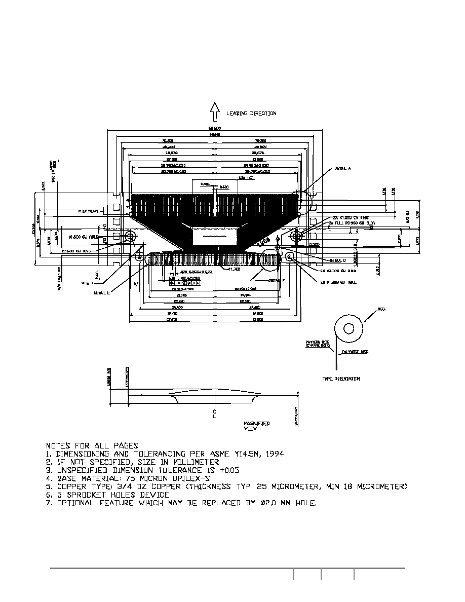
Solomon Systech
Mar 2002
Rev 1.3
SSD1809
P 25/27
P 25/27
P 25/27
P 25/27
P 25/27
P 25/27
P 25/27
P 25/27
P 25/27
P 25/27
P 25/27
P 25/27
PACKAGE DIMENSIONS
SSD1809T
TAB PACKAGE DIMENSION - 1

SSD1809
Rev 1.3
Mar 2002
Solomon Systech
P 26/27
PACKAGE DIMENSIONS
SSD1809T
TAB PACKAGE DIMENSION - 2

Solomon Systech reserves the right to make changes without further notice to any products herein. Solomon Systech makes no warra nty, representation or guar-
antee regarding the suitability of its products for any particular purpose, nor does Solomon Systech assume any liability arising out of the application or use of any
product or circuit, and specifically disclaims any and all liability, including without limitation consequential or incidental d amages. "Typical" parameters can and do
vary in different applications. All operating parameters, including "Typicals" must be validated for each customer application by customer's technical experts.
Solomon Systech does not convey any license under its patent rights nor the rights of others. Solomon Systech products are not designed, intended, or autho-
rized for use as components in systems intended for surgical implant into the body, or other applications intended to support or sustain life, or for any other appli-
cation in which the failure of the Solomon Systech product could create a situation where personal injury or death may occur. Should Buyer purchase or use
Solomon Systech products for any such unintended or unauthorized application, Buyer shall indemnify and hold Solomon Systech and its offices, employees,
subsidiaries, affiliates, and distributors harmless against all claims, costs, damages, and expenses, and reasonable attorney fe es arising out of, directly or indi-
rectly, any claim of personal injury or death associated with such unintended or unauthorized use, even if such claim alleges th at Solomon Systech was negligent
regarding the design or manufacture of the part.
Solomon Systech
Mar 2002
Rev 1.3
SSD1809
P 27/27
http://www.solomon-systech.com