
TABLE OF CONTENTS
1.
GENERAL DESCRIPTION ................................................................................................................ 1
2.
FEATURES ........................................................................................................................................ 1
3.
ORDERING INFORMATION ............................................................................................................. 1
4.
BLOCK DIAGRAM ............................................................................................................................ 2
5.
SSD1881Z DIE PAD ASSIGNMENT ................................................................................................. 3
6.
SSD1881TR TAB PIN ASSIGNMENT............................................................................................... 6
7.
SSD1881T1R1 TAB PIN ASSIGNMENT........................................................................................... 8
8.
SSD1881T2R TAB PIN ASSIGNMENT........................................................................................... 10
9.
PIN DESCRIPTION.......................................................................................................................... 12
VDD_ROW, +V1, VC, -V1 (Power Pin) ................................................................................................ 12
YD (Input Pin) ....................................................................................................................................... 12
LP (Input Pin)........................................................................................................................................ 12
FR (Input Pin) ....................................................................................................................................... 12
F1, F2 (Input Pin).................................................................................................................................. 12
DOFF# (Input Pin) ................................................................................................................................ 12
SEL (Input Pin) ..................................................................................................................................... 12
CIO1, CIO2 (I/O Pin) ............................................................................................................................. 12
SHL (Input Pin) ..................................................................................................................................... 13
LSEL (Input Pin) ................................................................................................................................... 13
CSEL (Input Pin)................................................................................................................................... 13
TEST1 (Input Pin) ................................................................................................................................. 13
TEST2 (Input Pin, only exists on gold-bumped die)......................................................................... 13
COM0-COM159 (Output Pin) ............................................................................................................... 13
NCx and DUMCORx (Dummy Pin)...................................................................................................... 13

10.
FUNCTIONAL BLOCK DESCRIPTIONS ........................................................................................ 14
Controller and Data Register .............................................................................................................. 14
Bi-directional Shift Register ............................................................................................................... 14
Common Cell Level Shifter ................................................................................................................. 14
Timing Diagram For 1/160 duty and 1P operation (DOFF# = H and FR=L) .................................... 15
Timing Diagram For 1/160 duty and 1P operation (DOFF# = H and FR=H).................................... 16
Timing Diagram For 1/160 duty and 1/2P operation (DOFF# = H and FR = L) ............................... 17
Timing Diagram For 1/160 duty and 1/2P operation (DOFF# = H and FR = H)............................... 18
11.
MAXIMUM RATINGS....................................................................................................................... 18
12.
DC CHARACTERISTICS................................................................................................................. 20
13.
AC CHARACTERISTICS................................................................................................................. 21
Input Timing Characteristics .............................................................................................................. 21
Output Timing Characteristics ........................................................................................................... 22
14.
PRECAUTION.................................................................................................................................. 23
15.
APPLICATION EXAMPLE ≠ 160 X 160 LCD SYSTEM.................................................................. 25
16.
PACKAGE DIMENSION .................................................................................................................. 26

SOLOMON SYSTECH
SEMICONDUCTOR TECHNICAL DATA
This document contains information on a new product under definition stage. Solomon Systech Limited reserves
the right to change or discontinue this product without notice.
http://www.solomon-systech.com
SSD1881
Rev 2.1
P 1
Sep 2002
Copyright
2003 Solomon Systech Limited
SSD1881
Advance Information
SSD1881 MLA ROW (COMMON) DRIVER
CMOS
1. GENERAL DESCRIPTION
The SSD1881 is an MLA (Multi Line Addressing), 160 outputs and triple-value low resistance common driver. Joining with the
SSD1730 MLA power chip and the SSD1870 column driver, an MLA LCD module system having high picture quality, high
speed responses and low power consumption can be produced. SSD1881 can be configured as 140 outputs or 160 outputs.
2. FEATURES
Power supply to logic system, 2.7V - 5.5V
LCD drive voltage, 14V - 30V
140 or 160 common outputs
Drive duty, 1/160 and 1/320
1/2P and 1P operation mode
Adjustable LCD power source offset bias
Non-biased display off function
Seletable output shift direction
Cascade supported
Available in Gold-bumped die and TAB (Tape Automated Bonding) Package
3. ORDERING INFORMATION
Table 1 - Ordering part number
Ordering Part
Number
Output lead pitch
(mm)
Package Form
SSD1881Z
N/A
Gold Bump Die
SSD1881TR 0.2295
TAB
SSD1881T1R1 0.14
TAB
SSD1881T2R 0.22
TAB

Solomon Systech
Sep 2003
P 2
Rev 2.1
SSD1881
4. BLOCK DIAGRAM
Figure 1 - Block Diagram of SSD1881
Common Cell
Level Shifter
COM0 ~ COM159
Data Register
160 bits
Controller
Bi-directional Shift Register
40 bits
VDD_ROW
V
SS
+V
1
V
C
-V
1
DOFF#
TEST1
FR
F1
F2
LP
CIO1
YD
SHL SEL LSEL CSEL
CIO2
SSD1881
Rev 2.1
P 3
Aug 2003
Solomon Systech
5. SSD1881Z DIE PAD ASSIGNMENT
C
ente
r
: -
2
2
54.57
5,-
272.
225
Si
z
e
:
2
6
.
8u
m
x
27
.
2
um
C
ent
er
:
-
174
9.
825,
-
305.
25
S
i
ze:
70um
x 70um
C
ent
e
r
:
-
2497.
65,
-
2
80.
8
S
i
ze:
94
.
5um
x
94.
5um
Gold Bump Alignment Mark
This alignment mark contains gold bump for
IC bumping process alignment and IC
identifications. No conductive tracks should
be laid underneath this mark to avoid short
circuit.
COM22
COM21
COM20
COM19
COM18
COM17
COM16
COM15
COM14
COM13
COM12
COM11
COM10
COM9
COM8
COM7
COM6
COM5
COM4
COM3
COM2
COM1
COM0
NC29
NC28
NC27
+V
1
+V
1
+V
1
VC
VC
VC
-V
1
-V
1
-V
1
NC26
NC25
NC24
NC23
NC22
NC21
NC20
NC19
NC18
NC17
NC16
TEST2
TEST1
F2
F2
F1
F1
YD
YD
CIO1
CIO1
CIO2
CIO2
LP
LP
CSEL
FR
DOFF#
LSEL
VDD_ROW
VDD_ROW
VDD_ROW
SEL
SHL
NC15
NC14
NC13
NC12
NC11
NC10
NC9
NC8
NC7
NC6
NC5
NC4
NC3
NC2
-V
1
-V
1
-V
1
VC
VC
VC
+V
1
+V
1
+V
1
NC1
COM159
COM158
COM157
COM156
COM155
COM154
COM153
COM152
COM151
COM150
COM149
COM178
COM147
COM146
COM145
COM144
COM143
COM142
COM141
COM140
COM139
COM138
DU
M
C
O
R
3
NC36
NC37
NC38
NC39
NC40
NC41
DU
M
C
O
R
4
DU
M
C
O
R
2
NC
3
5
NC
3
4
NC
3
3
NC
3
2
NC
3
1
NC
3
0
DU
M
C
O
R
1
COM23
COM24
COM25
COM26
COM27
COM28
COM29
COM30
COM31
COM32
COM33
COM34
COM35
COM36
COM37
COM38
COM39
COM40
COM41
COM42
COM43
COM44
COM45
COM46
COM47
COM48
COM49
COM50
COM51
COM52
COM53
COM54
COM55
COM56
COM57
COM58
COM59
COM60
COM61
COM62
COM63
COM64
COM65
COM66
COM67
COM68
COM69
COM70
COM71
COM72
COM73
COM74
COM75
COM76
COM77
COM78
COM79
COM80
COM81
COM82
COM83
COM84
COM85
COM86
COM87
COM88
COM89
COM90
COM91
COM92
COM93
COM94
COM95
COM96
COM97
COM98
COM99
COM100
COM101
COM102
COM103
COM104
COM105
COM106
COM107
COM108
COM109
COM110
COM111
COM112
COM113
COM114
COM115
COM116
COM117
COM118
COM119
COM120
COM121
COM122
COM123
COM124
COM125
COM126
COM127
COM128
COM129
COM130
COM131
COM132
COM133
COM134
COM135
COM136
COM137
Pad #1
C
ent
er
:
2389.
675,
-
2
80.
8
S
i
ze:
94.
5um
x
9
4
.
5um
Figure 2 ≠ SSD1881Z Die Pad Assignment
Y
X
SSD1881
Pad 1,2,3.......116
Die Size: 12233.7um X 1356.1um
Bump Size: 60.2um X 60.2um
Die Thickness: 533um

Solomon Systech
Sep 2003
P 4
Rev 2.1
SSD1881
Table 2 - SSD1881Z Die Pad Coordinates
Pad#
Pin Name
X-pos
Y-pos
Pad#
Pin Name
X-pos
Y-pos
Pad#
Pin Name
X-pos
Y-pos
1
COM138
-5768.400
-507.000
61
CIO1
303.600
-507.000
121
NC34
5965.050
187.450
2
COM139
-5667.200
-507.000
62
YD
404.800
-507.000
122
NC35
5965.050
288.650
3
COM140
-5566.000
-507.000
63
YD
506.000
-507.000
123
DUMCOR2
5965.050
507.000
4
COM141
-5464.800
-507.000
64
F1
607.200
-507.000
124
COM23
5768.400
507.000
5
COM142
-5363.600
-507.000
65
F1
708.400
-507.000
125
COM24
5667.200
507.000
6
COM143
-5262.400
-507.000
66
F2
809.600
-507.000
126
COM25
5566.000
507.000
7
COM144
-5161.200
-507.000
67
F2
910.800
-507.000
127
COM26
5464.800
507.000
8
COM145
-5060.000
-507.000
68
TEST1
1012.000
-507.000
128
COM27
5363.600
507.000
9
COM146
-4958.800
-507.000
69
TEST2
1113.200
-507.000
129
COM28
5262.400
507.000
10
COM147
-4857.600
-507.000
70
NC16
1214.400
-507.000
130
COM29
5161.200
507.000
11
COM178
-4756.400
-507.000
71
NC17
1315.600
-507.000
131
COM30
5060.000
507.000
12
COM149
-4655.200
-507.000
72
NC18
1416.800
-507.000
132
COM31
4958.800
507.000
13
COM150
-4554.000
-507.000
73
NC19
1518.000
-507.000
133
COM32
4857.600
507.000
14
COM151
-4452.800
-507.000
74
NC20
1619.200
-507.000
134
COM33
4756.400
507.000
15
COM152
-4351.600
-507.000
75
NC21
1720.400
-507.000
135
COM34
4655.200
507.000
16
COM153
-4250.400
-507.000
76
NC22
1821.600
-507.000
136
COM35
4554.000
507.000
17
COM154
-4149.200
-507.000
77
NC23
1922.800
-507.000
137
COM36
4452.800
507.000
18
COM155
-4048.000
-507.000
78
NC24
2024.000
-507.000
138
COM37
4351.600
507.000
19
COM156
-3946.800
-507.000
79
NC25
2125.200
-507.000
139
COM38
4250.400
507.000
20
COM157
-3845.600
-507.000
80
NC26
2226.400
-507.000
140
COM39
4149.200
507.000
21
COM158
-3744.400
-507.000
81
-V1
2327.600
-507.000
141
COM40
4048.000
507.000
22
COM159
-3643.200
-507.000
82
-V1
2428.800
-507.000
142
COM41
3946.800
507.000
23
NC1
-3542.000
-507.000
83
-V1
2530.000
-507.000
143
COM42
3845.600
507.000
24
+V1
-3440.800
-507.000
84
VC
2631.200
-507.000
144
COM43
3744.400
507.000
25
+V1
-3339.600
-507.000
85
VC
2732.400
-507.000
145
COM44
3643.200
507.000
26
+V1
-3238.400
-507.000
86
VC
2833.600
-507.000
146
COM45
3542.000
507.000
27
VC
-3137.200
-507.000
87
+V1
2934.800
-507.000
147
COM46
3440.800
507.000
28
VC
-3036.000
-507.000
88
+V1
3036.000
-507.000
148
COM47
3339.600
507.000
29
VC
-2934.800
-507.000
89
-V1
3137.200
-507.000
149
COM48
3238.400
507.000
30
-V1
-2833.600
-507.000
90
NC27
3238.400
-507.000
150
COM49
3137.200
507.000
31
-V1
-2732.400
-507.000
91
NC28
3339.600
-507.000
151
COM50
3036.000
507.000
32
-V1
-2631.200
-507.000
92
NC29
3440.800
-507.000
152
COM51
2934.800
507.000
33
NC2
-2530.000
-507.000
93
COM0
3542.000
-507.000
153
COM52
2833.600
507.000
34
NC3
-2428.800
-507.000
94
COM1
3643.200
-507.000
154
COM53
2732.400
507.000
35
NC4
-2327.600
-507.000
95
COM2
3744.400
-507.000
155
COM54
2631.200
507.000
36
NC5
-2226.400
-507.000
96
COM3
3845.600
-507.000
156
COM55
2530.000
507.000
37
NC6
-2125.200
-507.000
97
COM4
3946.800
-507.000
157
COM56
2428.800
507.000
38
NC7
-2024.000
-507.000
98
COM5
4048.000
-507.000
158
COM57
2327.600
507.000
39
NC8
-1922.800
-507.000
99
COM6
4149.200
-507.000
159
COM58
2226.400
507.000
40
NC9
-1821.600
-507.000
100
COM7
4250.400
-507.000
160
COM59
2125.200
507.000
41
NC10
-1720.400
-507.000
101
COM8
4351.600
-507.000
161
COM60
2024.000
507.000
42
NC11
-1619.200
-507.000
102
COM9
4452.800
-507.000
162
COM61
1922.800
507.000
43
NC12
-1518.000
-507.000
103
COM10
4554.000
-507.000
163
COM62
1821.600
507.000
44
NC13
-1416.800
-507.000
104
COM11
4655.200
-507.000
164
COM63
1720.400
507.000
45
NC14
-1315.600
-507.000
105
COM12
4756.400
-507.000
165
COM64
1619.200
507.000
46
NC15
-1214.400
-507.000
106
COM13
4857.600
-507.000
166
COM65
1518.000
507.000
47
SHL
-1113.200
-507.000
107
COM14
4958.800
-507.000
167
COM66
1416.800
507.000
48
SEL
-1012.000
-507.000
108
COM15
5060.000
-507.000
168
COM67
1315.600
507.000
49
VDD_ROW
-910.800
-507.000
109
COM16
5161.200
-507.000
169
COM68
1214.400
507.000
50
VDD_ROW
-809.600
-507.000
110
COM17
5262.400
-507.000
170
COM69
1113.200
507.000
51
VDD_ROW
-708.400
-507.000
111
COM18
5363.600
-507.000
171
COM70
1012.000
507.000
52
LSEL
-607.200
-507.000
112
COM19
5464.800
-507.000
172
COM71
910.800
507.000
53
-506.000
-507.000
113
COM20
5566.000
-507.000
173
COM72
809.600
507.000
54
FR
-404.800
-507.000
114
COM21
5667.200
-507.000
174
COM73
708.400
507.000
55
CSEL
-303.600
-507.000
115
COM22
5768.400
-507.000
175
COM74
607.200
507.000
56
LP
-202.400
-507.000
116
DUMCOR1
5965.050
-507.000
176
COM75
506.000
507.000
57
LP
-101.200
-507.000
117
NC30
5965.050
-288.650
177
COM76
404.800
507.000
58
CIO2
0.000
-507.000
118
NC31
5965.050
-187.450
178
COM77
303.600
507.000
59
CIO2
101.200
-507.000
119
NC32
5965.050
-86.250
179
COM78
202.400
507.000
60
CIO1
202.400
-507.000
120
NC33
5965.050
86.250
180
COM79
101.200
507.000
DOFF#

SSD1881
Rev 2.1
P 5
Aug 2003
Solomon Systech
Pad#
Pin Name
X-pos
Y-pos
Pad#
Pin Name
X-pos
Y-pos
181
COM80
0.000
507.000
241
NC37
-5965.050
187.450
182
COM81
-101.200
507.000
242
NC38
-5965.050
86.250
183
COM82
-202.400
507.000
243
NC39
-5965.050
-86.250
184
COM83
-303.600
507.000
244
NC40
-5965.050 -187.450
185
COM84
-404.800
507.000
245
NC41
-5965.050 -288.650
186
COM85
-506.000
507.000
246
DUMCOR4
-5965.050 -507.000
187
COM86
-607.200
507.000
188
COM87
-708.400
507.000
189
COM88
-809.600
507.000
190
COM89
-910.800
507.000
191
COM90
-1012.000
507.000
192
COM91
-1113.200
507.000
193
COM92
-1214.400
507.000
194
COM93
-1315.600
507.000
195
COM94
-1416.800
507.000
196
COM95
-1518.000
507.000
197
COM96
-1619.200
507.000
198
COM97
-1720.400
507.000
199
COM98
-1821.600
507.000
200
COM99
-1922.800
507.000
201
COM100
-2024.000
507.000
202
COM101
-2125.200
507.000
203
COM102
-2226.400
507.000
204
COM103
-2327.600
507.000
205
COM104
-2428.800
507.000
206
COM105
-2530.000
507.000
207
COM106
-2631.200
507.000
208
COM107
-2732.400
507.000
209
COM108
-2833.600
507.000
210
COM109
-2934.800
507.000
211
COM110
-3036.000
507.000
212
COM111
-3137.200
507.000
213
COM112
-3238.400
507.000
214
COM113
-3339.600
507.000
215
COM114
-3440.800
507.000
216
COM115
-3542.000
507.000
217
COM116
-3643.200
507.000
218
COM117
-3744.400
507.000
219
COM118
-3845.600
507.000
220
COM119
-3946.800
507.000
221
COM120
-4048.000
507.000
222
COM121
-4149.200
507.000
223
COM122
-4250.400
507.000
224
COM123
-4351.600
507.000
225
COM124
-4452.800
507.000
226
COM125
-4554.000
507.000
227
COM126
-4655.200
507.000
228
COM127
-4756.400
507.000
229
COM128
-4857.600
507.000
230
COM129
-4958.800
507.000
231
COM130
-5060.000
507.000
232
COM131
-5161.200
507.000
233
COM132
-5262.400
507.000
234
COM133
-5363.600
507.000
235
COM134
-5464.800
507.000
236
COM135
-5566.000
507.000
237
COM136
-5667.200
507.000
238
COM137
-5768.400
507.000
239
DUMCOR3
-5965.050
507.000
240
NC36
-5965.050
288.650

Solomon Systech
Sep 2003
P 6
Rev 2.1
SSD1881
6. SSD1881TR TAB PIN ASSIGNMENT
Figure 3 ≠ SSD1881TR Pin Assignment (Copper View, Normal TAB Design)
SSD1881
Rev 2.1
P 7
Aug 2003
Solomon Systech
Table 3 ≠ SSD1881TR Pin Assignment
Tab Pin# Signal Name
Tab Pin# Signal Name
Tab Pin# Signal Name
Tab Pin# Signal Name
1
NC
61
COM34
121
COM94
181
COM154
2
62
COM35
122
COM95
182
COM155
3
VC
63
COM36
123
COM96
183
COM156
4
64
COM37
124
COM97
184
COM157
5
SHL
65
COM38
125
COM98
185
COM158
6
SEL
66
COM39
126
COM99
186
COM159
7
VDD_ROW
67
COM40
127
COM100
187
NC
8
LSEL
68
COM41
128
COM101
188
NC
9
69
COM42
129
COM102
189
NC
10
FR
70
COM43
130
COM103
11
CSEL
71
COM44
131
COM104
12
LP
72
COM45
132
COM105
13
CIO2
73
COM46
133
COM106
14
CIO1
74
COM47
134
COM107
15
YD
75
COM48
135
COM108
16
DUMMY
76
COM49
136
COM109
17
F1
77
COM50
137
COM110
18
F2
78
COM51
138
COM111
19
TEST1
79
COM52
139
COM112
20
80
COM53
140
COM113
21
VC
81
COM54
141
COM114
22
82
COM55
142
COM115
23
NC
83
COM56
143
COM116
24
NC
84
COM57
144
COM117
25
NC
85
COM58
145
COM118
26
NC
86
COM59
146
COM119
27
COM0
87
COM60
147
COM120
28
COM1
88
COM61
148
COM121
29
COM2
89
COM62
149
COM122
30
COM3
90
COM63
150
COM123
31
COM4
91
COM64
151
COM124
32
COM5
92
COM65
152
COM125
33
COM6
93
COM66
153
COM126
34
COM7
94
COM67
154
COM127
35
COM8
95
COM68
155
COM128
36
COM9
96
COM69
156
COM129
37
COM10
97
COM70
157
COM130
38
COM11
98
COM71
158
COM131
39
COM12
99
COM72
159
COM132
40
COM13
100
COM73
160
COM133
41
COM14
101
COM74
161
COM134
42
COM15
102
COM75
162
COM135
43
COM16
103
COM76
163
COM136
44
COM17
104
COM77
164
COM137
45
COM18
105
COM78
165
COM138
46
COM19
106
COM79
166
COM139
47
COM20
107
COM80
167
COM140
48
COM21
108
COM81
168
COM141
49
COM22
109
COM82
169
COM142
50
COM23
110
COM83
170
COM143
51
COM24
111
COM84
171
COM144
52
COM25
112
COM85
172
COM145
53
COM26
113
COM86
173
COM146
54
COM27
114
COM87
174
COM147
55
COM28
115
COM88
175
COM148
56
COM29
116
COM89
176
COM149
57
COM30
117
COM90
177
COM150
58
COM31
118
COM91
178
COM151
59
COM32
119
COM92
179
COM152
60
COM33
120
COM93
180
COM153
-V
1
-V
1
+V
1
+V
1
DOFF#
Solomon Systech
Sep 2003
P 8
Rev 2.1
SSD1881
7. SSD1881T1R1 TAB PIN ASSIGNMENT
Figure 4 ≠ SSD1881T1R1 Pin Assignment (Copper View, Normal TAB Design)

SSD1881
Rev 2.1
P 9
Aug 2003
Solomon Systech
Table 4 ≠ SSD1881T1R1 Pin Assignment
Tab Pin# Signal Name
Tab Pin# Signal Name
Tab Pin# Signal Name
Tab Pin# Signal Name
1
NC
61
COM35
121
COM95
181
COM155
2
62
COM36
122
COM96
182
COM156
3
VC
63
COM37
123
COM97
183
COM157
4
64
COM38
124
COM98
184
COM158
5
SHL
65
COM39
125
COM99
185
COM159
6
SEL
66
COM40
126
COM100
186
NC
7
VDD_ROW
67
COM41
127
COM101
8
LSEL
68
COM42
128
COM102
9
69
COM43
129
COM103
10
FR
70
COM44
130
COM104
11
CSEL
71
COM45
131
COM105
12
LP
72
COM46
132
COM106
13
CIO2
73
COM47
133
COM107
14
CIO1
74
COM48
134
COM108
15
YD
75
COM49
135
COM109
16
DUMMY
76
COM50
136
COM110
17
F1
77
COM51
137
COM111
18
F2
78
COM52
138
COM112
19
TEST1
79
COM53
139
COM113
20
80
COM54
140
COM114
21
VC
81
COM55
141
COM115
22
82
COM56
142
COM116
23
NC
83
COM57
143
COM117
24
NC
84
COM58
144
COM118
25
NC
85
COM59
145
COM119
26
COM0
86
COM60
146
COM120
27
COM1
87
COM61
147
COM121
28
COM2
88
COM62
148
COM122
29
COM3
89
COM63
149
COM123
30
COM4
90
COM64
150
COM124
31
COM5
91
COM65
151
COM125
32
COM6
92
COM66
152
COM126
33
COM7
93
COM67
153
COM127
34
COM8
94
COM68
154
COM128
35
COM9
95
COM69
155
COM129
36
COM10
96
COM70
156
COM130
37
COM11
97
COM71
157
COM131
38
COM12
98
COM72
158
COM132
39
COM13
99
COM73
159
COM133
40
COM14
100
COM74
160
COM134
41
COM15
101
COM75
161
COM135
42
COM16
102
COM76
162
COM136
43
COM17
103
COM77
163
COM137
44
COM18
104
COM78
164
COM138
45
COM19
105
COM79
165
COM139
46
COM20
106
COM80
166
COM140
47
COM21
107
COM81
167
COM141
48
COM22
108
COM82
168
COM142
49
COM23
109
COM83
169
COM143
50
COM24
110
COM84
170
COM144
51
COM25
111
COM85
171
COM145
52
COM26
112
COM86
172
COM146
53
COM27
113
COM87
173
COM147
54
COM28
114
COM88
174
COM148
55
COM29
115
COM89
175
COM149
56
COM30
116
COM90
176
COM150
57
COM31
117
COM91
177
COM151
58
COM32
118
COM92
178
COM152
59
COM33
119
COM93
179
COM153
60
COM34
120
COM94
180
COM154
-V
1
-V
1
+V
1
+V
1
DOFF#

Solomon Systech
Sep 2003
P 10
Rev 2.1
SSD1881
8. SSD1881T2R TAB PIN ASSIGNMENT
Figure 5 ≠ SSD1881T2R Pin Assignment (Copper View, Normal TAB Design)
SSD1881
Rev 2.1
P 11
Aug 2003
Solomon Systech
Table 5 ≠ SSD1881T2R Pin Assignment
PIN#
NAME
PIN#
NAME
PIN#
NAME
PIN#
NAME
1
NC
51
COM24
101
COM74
151
COM124
2
+V1
52
COM25
102
COM75
152
COM125
3
VC
53
COM26
103
COM76
153
COM126
4
-V1
54
COM27
104
COM77
154
COM127
5
SHL
55
COM28
105
COM78
155
COM128
6
SEL
56
COM29
106
COM79
156
COM129
7
VDD_ROW
57
COM30
107
COM80
157
COM130
8
LSEL
58
COM31
108
COM81
158
COM131
9
DOFF#
59
COM32
109
COM82
159
COM132
10
FR
60
COM33
110
COM83
160
COM133
11
CSEL
61
COM34
111
COM84
161
COM134
12
LP
62
COM35
112
COM85
162
COM135
13
CIO2
63
COM36
113
COM86
163
COM136
14
CIO1
64
COM37
114
COM87
164
COM137
15
YD
65
COM38
115
COM88
165
COM138
16
DUMMY
66
COM39
116
COM89
166
COM139
17
F1
67
COM40
117
COM90
167
COM140
18
F2
68
COM41
118
COM91
168
COM141
19
TEST1
69
COM42
119
COM92
169
COM142
20
-V1
70
COM43
120
COM93
170
COM143
21
VC
71
COM44
121
COM94
171
COM144
22
+V1
72
COM45
122
COM95
172
COM145
23
NC
73
COM46
123
COM96
173
COM146
24
NC
74
COM47
124
COM97
174
COM147
25
NC
75
COM48
125
COM98
175
COM148
26
NC
76
COM49
126
COM99
176
COM149
27
COM0
77
COM50
127
COM100
177
COM150
28
COM1
78
COM51
128
COM101
178
COM151
29
COM2
79
COM52
129
COM102
179
COM152
30
COM3
80
COM53
130
COM103
180
COM153
31
COM4
81
COM54
131
COM104
181
COM154
32
COM5
82
COM55
132
COM105
182
COM155
33
COM6
83
COM56
133
COM106
183
COM156
34
COM7
84
COM57
134
COM107
184
COM157
35
COM8
85
COM58
135
COM108
185
COM158
36
COM9
86
COM59
136
COM109
186
COM159
37
COM10
87
COM60
137
COM110
187
NC
38
COM11
88
COM61
138
COM111
188
NC
39
COM12
89
COM62
139
COM112
40
COM13
90
COM63
140
COM113
41
COM14
91
COM64
141
COM114
42
COM15
92
COM65
142
COM115
43
COM16
93
COM66
143
COM116
44
COM17
94
COM67
144
COM117
45
COM18
95
COM68
145
COM118
46
COM19
96
COM69
146
COM119
47
COM20
97
COM70
147
COM120
48
COM21
98
COM71
148
COM121
49
COM22
99
COM72
149
COM122
50
COM23
100
COM73
150
COM123

Solomon Systech
Sep 2003
P 12
Rev 2.1
SSD1881
9. PIN DESCRIPTION
VDD_ROW, +V1, VC, -V1 (Power Pin)
VDD_ROW is a power pin to supply power to the logic system. The voltage range is 2.7V to 5.5V with respect to the -V1 pin.
+V1, VC and -V1 are power supply pins to the LCD system. Their relationship is +V1
VC
VDD_ROW
-V1.
YD (Input Pin)
This input pin is used as a signal to start a frame and to reset the column address for writing. (Refer to Note 1)
LP (Input Pin)
This is an input pin and is used as a display data latch clock. The display data is latched at the falling edge of LP. (Refer to
Note 1)
FR (Input Pin)
This is an input pin and is used to change the LCD driving waveform polarity. If a power chip SSD1730 is used, the output FR
from the power chip should be connected to the FR pin of the row driver. (Refer to Note 1)
F1, F2 (Input Pin)
These are input pins and are used as driver pattern select signals. These two signals are generated by a column driver. If a
display system is formed by the column driver SSD1870 and the row driver SSD1881, outputs F10 and F20 from the column
driver should be connected to F1 and F2 of the row driver respectively. (Refer to Note 1)
DOFF# (Input Pin)
This is an input pin and is used to control the LC display. When it is set at "L" level, all common outputs are forced to V
C
level
and the LC display will be forced to blank, however, the contents of the latches are maintained. In the normal display operation,
it is set to "H" level. (Refer to Note 1)
SEL (Input Pin)
SSD1881 can be configured as 140 common outputs or 160 common outputs which is controlled by this input pin SEL.
When SEL is set at "L" level, 160 outputs are chosen and COM0 to COM159 will be used. When SEL is set at "H" level, 140
outputs are chosen and COM8 to COM147 will be used.
CIO1, CIO2 (I/O Pin)
These are I/O pins and they can be configured as an input or an output depending on the signal of SHL. When SHL is set at "L"
level, CIO1 is input and CIO2 is output. When SHL is set at "H" level, CIO1 is output and CIO2 is input. The output transition
occurs on the falling edge of LP. (Refer to Note 1)
SSD1881
Rev 2.1
P 13
Aug 2003
Solomon Systech
SHL (Input Pin)
This is an input pin and is used to select the output shift direction and to configure CIO1 and CIO2. Below table
shows the relationship between SEL, SHL, CIO1, CIO2 and the output shift direction.
SEL = L (160 common outputs)
SHL Output Shift Direction
CIO
CIO2
L
COM0 -> COM159
Input
Output
H
COM159 -> COM0
Output
Input
SEL = L (140 common outputs)
SHL Output Shift Direction
CIO
CIO2
L
COM8 -> COM147
Input
Output
H
COM147 -> COM8
Output
Input
Table 6 - Relationship between SEL, SHL, CIO2 and CIO2
LSEL (Input Pin)
This is an input pin and is used to select 1P Normal Operation or 1/2P Operation. That can cope with different
LCD having different response time.
When LSEL is set at "L" level, 1P Normal Operation is selected. when LSEL is set at "H" level, 1/2P Operation is
selected.
CSEL (Input Pin)
This is a chip select signal input. When only one common driver is used, CSEL should be set at "L" level. When
multiple common drivers are used, CSEL of the leading chip must be tied to "L" level and that of other chips must
be tied to "H" level.
TEST1 (Input Pin)
This is a reserved pin and it must be set at "L" level in the normal operation.
TEST2 (Input Pin, only exists on gold-bumped die)
This is a reserved pin and it must be set at "L" level in the normal operation.
COM0-COM159 (Output Pin)
These are output pins and provide common driving signals to the LCD panel. Output transition occurs at the falling
edge of LP.
NCx and DUMCORx (Dummy Pin)
These are NC pins and dummy pins. They must be left open & unconnected. Don't group the NC pins or dummy
pins together.
Note 1: If an MLA LCD system is formed by SSD1881 row driver, SSD1870 column driver and SSD1730 power chip, 1nF capacitors are
necessary for the capacitor coupling purpose. Refer to the Application example for circuit connection.
Solomon Systech
Sep 2003
P 14
Rev 2.1
SSD1881
10. FUNCTIONAL BLOCK DESCRIPTIONS
Controller and Data Register
Based on the input signal of FR, F1, F2 and LP, this Controller will generate signals to control the Data Register.
Then, the Data Register will latch the data to the Common Cell Level Shifter according to the signals from the
Controller and the data from the Shift Register. The data is latched to the Common Cell Level Shifter at the falling
edge of LP.
Bi-directional Shift Register
This Shift Register will shift the input signals YD and CIO input according to the setting of SHL, SEL, LSEL and
CSEL. When SHL is set at "L" level, CIO1 is input and CIO2 is output. When SHL is set at "H" level, CIO1 is
output and CIO2 is input. The output transition occurs on the falling edge of LP.
Common Cell Level Shifter
This is a level interface circuit which is used to convert the signal voltage level from a logic system level to the LCD
driver system voltage level. When DOFF# is at "L" level, all common output voltage will be at VC level. When
DOFF# is at "H" level, the common output voltage will be changed according to the status of input signals of FR,
F1 and F2.
Table 7 shows the relationship among the common output voltage and the input signals FR, F1 and F2. Table 8
shows the relationship between line number and Common.
F1
1
0
1
0
F1
1
0
1
0
F2
1
1
0
0
F2
1
1
0
0
line r
+V1
+V1
-V1
+V1
line r
-V1
-V1
+V1
-V1
line (r + 1)
-V1
+V1
+V1
+V1
line (r + 1)
+V1
-V1
-V1
-V1
line (r + 2)
+V1
-V1
+V1
+V1
line (r + 2)
-V1
+V1
-V1
-V1
line (r + 3)
+V1
+V1
+V1
-V1
line (r + 3)
-V1
-V1
-V1
+V1
When DOFF# = H and FR = L
When DOFF# = H and FR = H
Table 7 ≠ Relationship among COM voltage, F1, F2 and FR
Line number
Formula
Common
r
Multiples of 4
0, 4, 8, 12, ... , 148, 152, 156
r + 1
1 + multiples of 4
1, 5, 9, 13, ... , 149, 153, 157
r + 2
2 + multiples of 4
2, 6, 10, 14, ... , 150, 154, 158
r + 3
3 + multiples of 4
3, 7, 11, 15, ... , 151, 155, 159
Table 8 - Relationship between line number and Common.
SSD1881
Rev 2.1
P 15
Aug 2003
Solomon Systech
Timing Diagram For 1/160 duty and 1P operation (DOFF# = H and FR=L)
This diagram is for reference only. Below diagram is at the conditions of SHL = L, SEL = L, LSEL = L, CSEL = L
YD
LP
CIO
F1
F2
+V1
VC
-V1
+V1
VC
-V1
+V1
VC
-V1
+V1
VC
-V1
+V1
VC
-V1
+V1
VC
-V1
+V1
VC
-V1
+V1
VC
-V1
160
1
2
3
40
41
42
43
80
81
82
83
120
121
122
123
160
1
2
3
COM0
COM1
COM2
COM3
COM4
COM5
COM6
COM7
Figure 6 ≠ Timing diagram for 1/160 duty and 1P operation (DOFF# = H and FR = L)
Solomon Systech
Sep 2003
P 16
Rev 2.1
SSD1881
Timing Diagram For 1/160 duty and 1P operation (DOFF# = H and FR=H)
This diagram is for reference only., Below diagram is at the conditions of SHL = L, SEL = L, LSEL = L, CSEL = L
YD
LP
CIO
F1
F2
+V1
VC
-V1
+V1
VC
-V1
+V1
VC
-V1
+V1
VC
-V1
+V1
VC
-V1
+V1
VC
-V1
+V1
VC
-V1
+V1
VC
-V1
160
1
2
3
40
41
42
43
80
81
82
83
120
121
122
123
160
1
2
3
COM0
COM1
COM2
COM3
COM4
COM5
COM6
COM7
Figure 7 ≠ Timing diagram for 1/160 duty and 1P operation (DOFF# = H and FR = H)

SSD1881
Rev 2.1
P 17
Aug 2003
Solomon Systech
Timing Diagram For 1/160 duty and 1/2P operation (DOFF# = H and FR = L)
This diagram is for reference only. Below diagram is at the conditions of SHL = L, SEL = L, LSEL = H, CSEL = L
YD
LP
CIO
F1
F2
+V1
VC
-V1
+V1
VC
-V1
+V1
VC
-V1
+V1
VC
-V1
COM0
COM1
COM2
COM3
2/1
2/160
2/2
1/40
1/41
2/41
1/42
2/42
2/40
1/81
2/81
1/82
2/80
1/80
2/82
1/121
2/121
1/122
2/120
1/120
2/122
1/1
1/2
1/160
2/160
1/1
2/1
1/2
2/2
1/160
Figure 8 ≠ Timing diagram for 1/160 duty and 1/2P operation (DOFF# = H and FR = L)
Solomon Systech
Sep 2003
P 18
Rev 2.1
SSD1881
Timing Diagram For 1/160 duty and 1/2P operation (DOFF# = H and FR = H)
This diagram is for reference only. Below diagram is at the conditions of SHL = L, SEL = L, LSEL = H, CSEL = L
YD
LP
CIO
F1
F2
+V1
VC
-V1
+V1
VC
-V1
+V1
VC
-V1
+V1
VC
-V1
COM0
COM1
COM2
COM3
2/1
2/160
2/2
1/40
1/41
2/41
1/42
2/42
2/40
1/81
2/81
1/82
2/80
1/80
2/82
1/121
2/121
1/122
2/120
1/120
2/122
1/1
1/2
1/160
2/160
1/1
2/1
1/2
2/2
1/160
Figure 9 ≠ Timing diagram for 1/160 duty and 1/2P operation (DOFF# = H and FR = H)
11. MAXIMUM RATINGS
Symbol Parameter
Value
Unit

SSD1881
Rev 2.1
P 19
Aug 2003
Solomon Systech
VDD_ROW
Power Voltage
-0.3 to +7.0
V
+V1
-0.3 to 33
V
V
IN
Input Voltage
-V1 - 0.3 to +V1 + 0.3
V
V
o
Output Voltage
-V1 - 0.3 to +V1 + 0.3
V
I
Output current at CIO
20
mA
T
A
Operating temperature
-30 to +85
∞C
T
stg
Storage temperature
-65 to +150
∞C
Table 9 ≠ Maximum ratings for DC characteristics
Maximum ratings are those values beyond which damage to the device may occur. Functional operation should be
restricted to the limits shown in the DC characteristics section and the relationship between +V1, VC and -V1 must
be
+
V1
VCVDD_ROW-V1. All voltages are referenced to -V1 = 0V.
This device contains circuitry to protect the inputs against damage due to high static voltages of electric fields;
however, it is advised that normal precautions to be taken to avoid application of any voltage higher than maximum
rated voltages to this high impedance circuit. All dummy pins and NC pins must be left open & unconnected.
Don't group the NC pins together. The device may be light sensitive. Caution should be taken to avoid exposure
of this device to any light source during normal operation. This device is not radiation protected.

Solomon Systech
Sep 2003
P 20
Rev 2.1
SSD1881
12. DC CHARACTERISTICS
-V1 = 0.0V, VDD_ROW = 5.0V, T
A
= 25`C
Symbol Parameter
Test
Condition
Min Typ Max
Unit
VDD_ROW Power supply voltage
for logic system
2.7 5.0 5.5 V
+V1
VC
Power supply voltage
for LCD
-V1 = 0.0, VDD_ROW =
5.0V
14.0
--
--
+V1/2
30.0
--
V
V
I
DP1
Current drain from Pin
VDD_ROW
VDD_ROW=5.0V,
V
IN
=VDD_ROW, V
IL
=-V1,
freq of LP=16.8kHz and freq
of FR=70Hz, no loading
-- 6
25
µA
2
Current drain from Pin
+V1
+V1=30V, V
C
=+V1/2, -
V1=0.0V, VDD_ROW=5.0V,
V
IN
=VDD_ROW, V
IL
=-V1,
freq of LP=16.8kHz and freq
of FR=70Hz, no loading
-- 16 30
µA
I
SB
Static current drain
from Pin VDD_ROW
+V1 =14.0V to 30.0V, V
IN
=
VDD_ROW, V
IL
= -V1
-- 0.25 2 µA
V
IH
V
IL
Input High voltage at
pins: CIO1, CIO2,
SHL, SEL, LSEL,
CSEL, FR, YD, LP,
F1, F2 & DOFF#
Input Low voltage at
pins: CIO1, CIO2,
SHL, SEL, LSEL,
CSEL, FR, YD, LP,
F1, F2, TEST1 &
DOFF#
VDD_ROW = 2.7V to 5.5V
0.8*VDD_ROW
---
---
---
--
0.2*VDD_ROW
V
V
V
OH
V
OL
Output High voltage at
pins: CIO1 & CIO2
Output Low voltage at
pins: CIO1 & CIO2
VDD_ROW = 2.7V to 5.5V,
I
OH
= -0.3mA
VDD_ROW = 2.7V to 5.5V,
I
OL
= 0.3mA
VDD_ROW-0.4
--
--
--
--
0.4
V
V
I
L1
Input leakage current
at pins: SHL, SEL,
LSEL, CSEL, FR, YD,
LP, F1, F2, TEST1 &
DOFF#
-- -- 2
µA
I
L2
I/O leakage current at
pins: CIO1 & CIO2
-- -- 5
µA
Rout
Output resistance of
pins: COM0 ≠
COM159
-V1 = 0.0V, +V1 =30.0V,
V=0.5V
-- --
1000
Table 10 ≠ Electrical characteristics

SSD1881
Rev 2.1
P 21
Aug 2003
Solomon Systech
13. AC CHARACTERISTICS
Input Timing Characteristics
-V
1
= 0.0V, VDD_ROW = 5.0V, T
A
= 25
o
C
Symbol Parameter
Min
Typ
Max Unit
t
LPcyc
LP
period
500
-
-
ns
t
LPhi
LP pulse width (High level)
55
-
-
ns
t
LPlo
LP pulse width (Low level)
330
-
-
ns
t
YDs
YD, CIO setup time
100
-
-
ns
t
YDh
YD, CIO hold time
40
-
-
ns
t
YDset
YD --> LP allowable time
80
-
-
ns
t
F12s
F1, F2 setup time
100
-
-
ns
t
F12h
F1, F2 hold time
40
-
-
ns
t
FRs
FR setup time
100
-
-
ns
t
FRh
FR hold time
40
-
-
ns
t
r
Input signal rise time
-
-
50
ns
t
f
Input signal fall time
-
-
50
ns
Table 11 -
Input timing characteristics
Figure 10 ≠ Input timing characteristics
t
YDs
t
YDh
t
YDset
t
LPlo
t
r
t
f
t
LPhi
t
LPcyc
t
F12h
t
F12s
t
FRs
t
FRh
YD, CIO(Input)
LP
F1, F2
t
COM
Solomon Systech
Sep 2003
P 22
Rev 2.1
SSD1881
Output Timing Characteristics
-V
1
= 0.0V, VDD_ROW = 5.0V, T
A
= 25
o
C
Symbol Parameter Min
Typ
Max
Unit
t
COMd1
Delay time from LP to COM
- -
300
ns
t
COMd2
Delay time from DOFF# to COM
-
-
350
ns
t
CIOd
Delay time from LP to CIO output
-
-
700
ns
Table 12 ≠ Output timing characteristics
Figure 11 ≠ Output timing characteristics
t
CIOd
t
COMd2
LP
COM0 ~
COM239
CIO
(Output)
DOFF
t
COMd1
SSD1881
Rev 2.1
P 23
Aug 2003
Solomon Systech
14. PRECAUTION
When SSD1881 is used with SSD1870 column driver and SSD1730 power chip to form a low power display
system, the power supply of SSD1881 is actually coming from the SSD1730 outputs. Proper power up and power
down sequence must be followed to protect and to ensure proper functioning of the system.
The recommended power up and down sequence is as follow:
Power up:
∑
Pull DOFF# to L
∑
Provide power to the SSD1730 MLA power chip and SSD1870 MLA column driver.
∑
Provide LP pulses chain with other controller signals while keeping DOFF# at "L".
∑
Wait for a minimum of 150ms to allow the SSD1730 MLA power chip building up appropriate power levels of
the display system.
∑
Pull DOFF# to H to turn on the display
DOFF#
LP
Signals from LCD
controller
VDD_PWR
VDD_COL
VDD_ROW
Allow more than 150ms for a stable VDD_ROW
Figure 12 ≠ Recommended power up sequence
Solomon Systech
Sep 2003
P 24
Rev 2.1
SSD1881
Power down:
∑
Pull DOFF# to L to turn off the display
∑
Stop providing controller signals and LP pulses chain.
∑
Wait for a minimum of 500ms to allow the discharging of the power levels.
∑
Disconnect power from SSD1870 MLA column driver and SSD1730 MLA power chip.
DOFF#
LP
Signals from LCD
controller
VDD_PWR
VDD_COL
VDD_ROW
Allow more than 500ms for discharging
Figure 13 ≠ Recommended power down sequence

SSD1881
Rev 2.1
P 25
Aug 2003
Solomon Systech
15. APPLICATION EXAMPLE ≠ 160 X 160 LCD SYSTEM
Below figure shows an example of a 160 x 160 LCD system using the Power Chip SSD1730, the Row Driver
SSD1881 and the Column Driver SSD1870. In order to operate the system, power source is applied to V
DD
& V
SS
and a controller is used to issue signals to DOFF#, YD, LP, XSCL and data bus D0-D7.
SSD1870 Column Driver
EI
O
2
V
DD_
COL
VS
S
+V
3
+V
2
VC
-V
2
-V
3
F1
O
F2
O
SH
L
TE
ST
BS
EL
LS
E
L
FR
YD LP
XS
CL
D0
-
D
7
F1
S
F2
S
D
O
FF#
CA
SE
G
1
5
9
SEG
0
....................
SS
D
1881 R
o
w
D
r
iver
+V1
VC
-V1
SHL
SEL
VDD_ROW
LSEL
DOFF#
FR
CSEL
LP
CIO2
CIO1
YD
F1
F2
TEST1
COM159
COM0
......
SSD1730
EXTERNAL CIRCUITRY
INTERFACE TO CONTROLLER / MCU
VD
D
VSS
YD
LP
XSC
L
D0
-
D
7
D
O
FF#
+V3 / VDD_PWR
+V2
VC
-V2
-V3
FR
-V1
VDD_ROW
+V1
C1
C2
C3
C5
C6
C7
C9
C10
SEG
COM
160 x 160
LCD PANEL
C11
C8
EI
O
1
C4
Figure 14 ≠ 160 x 160 LCD system
Note 2 : 1nF capacitor is necessary for the capacitor coupling purpose.
Note 3 : Refer to the application circuit in the SSD1730 power chip specification.
Solomon Systech
Sep 2003
P 26
Rev 2.1
SSD1881
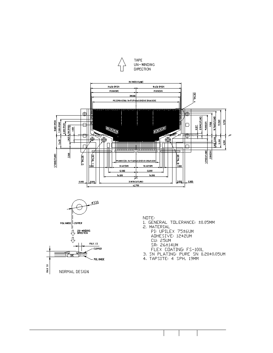
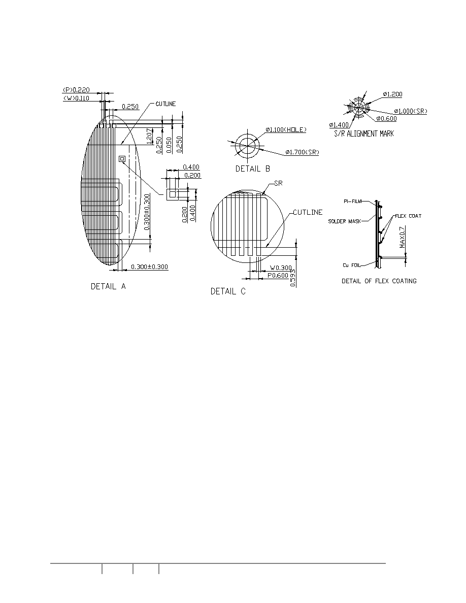
16. PACKAGE DIMENSION
SSD1881TR TAB Package Dimension ≠ 1
SSD1881
Rev 2.1
P 27
Aug 2003
Solomon Systech
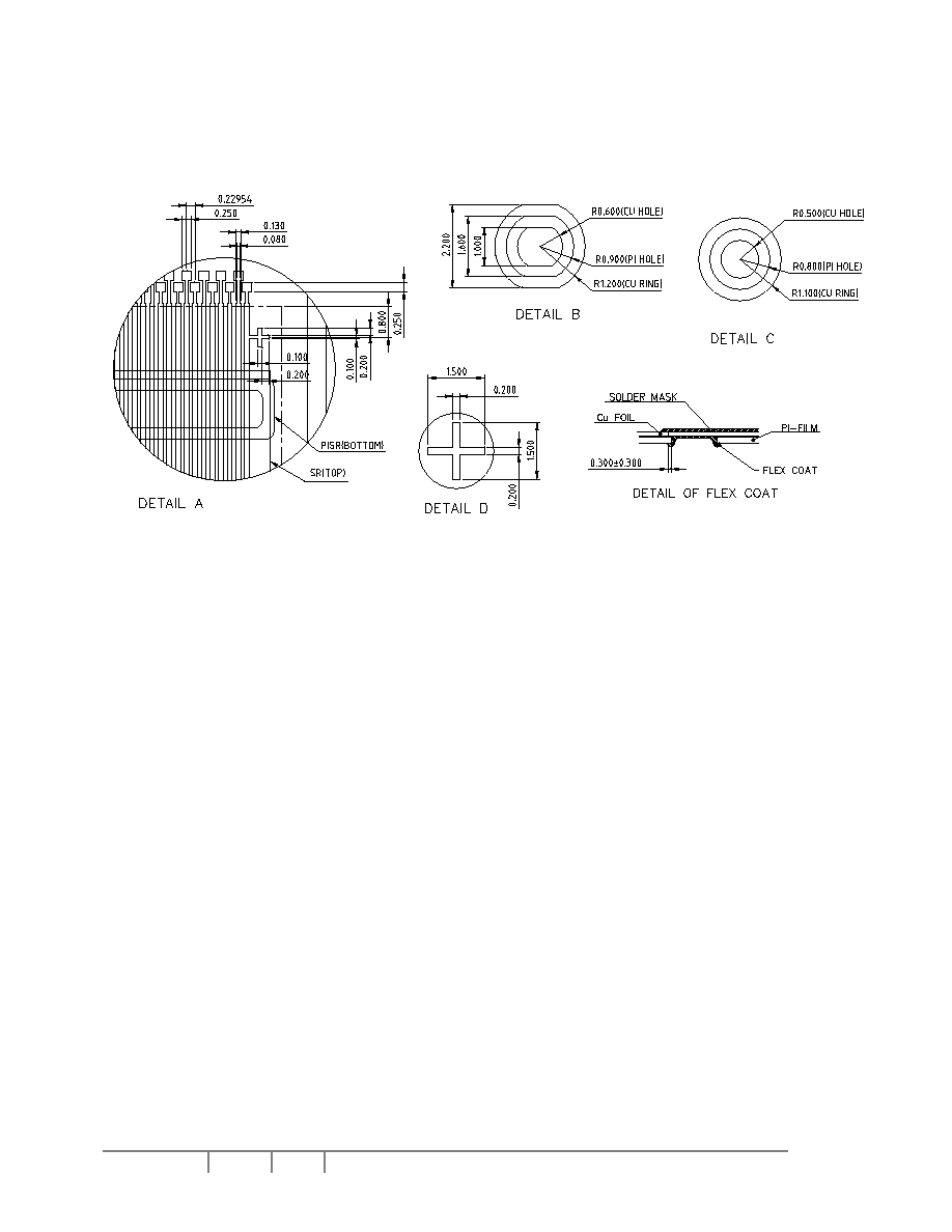
SSD1881TR TAB Package Dimension ≠ 2
Solomon Systech
Sep 2003
P 28
Rev 2.1
SSD1881
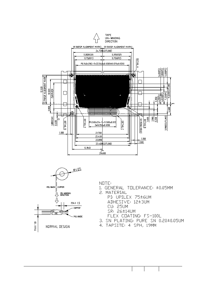
SSD1881T1R1 TAB PACKAGE DIMENSION ≠ 1

SSD1881
Rev 2.1
P 29
Aug 2003
Solomon Systech
SSD1881T1R1 TAB PACKAGE DIMENSION ≠ 2
Solomon Systech
Sep 2003
P 30
Rev 2.1
SSD1881
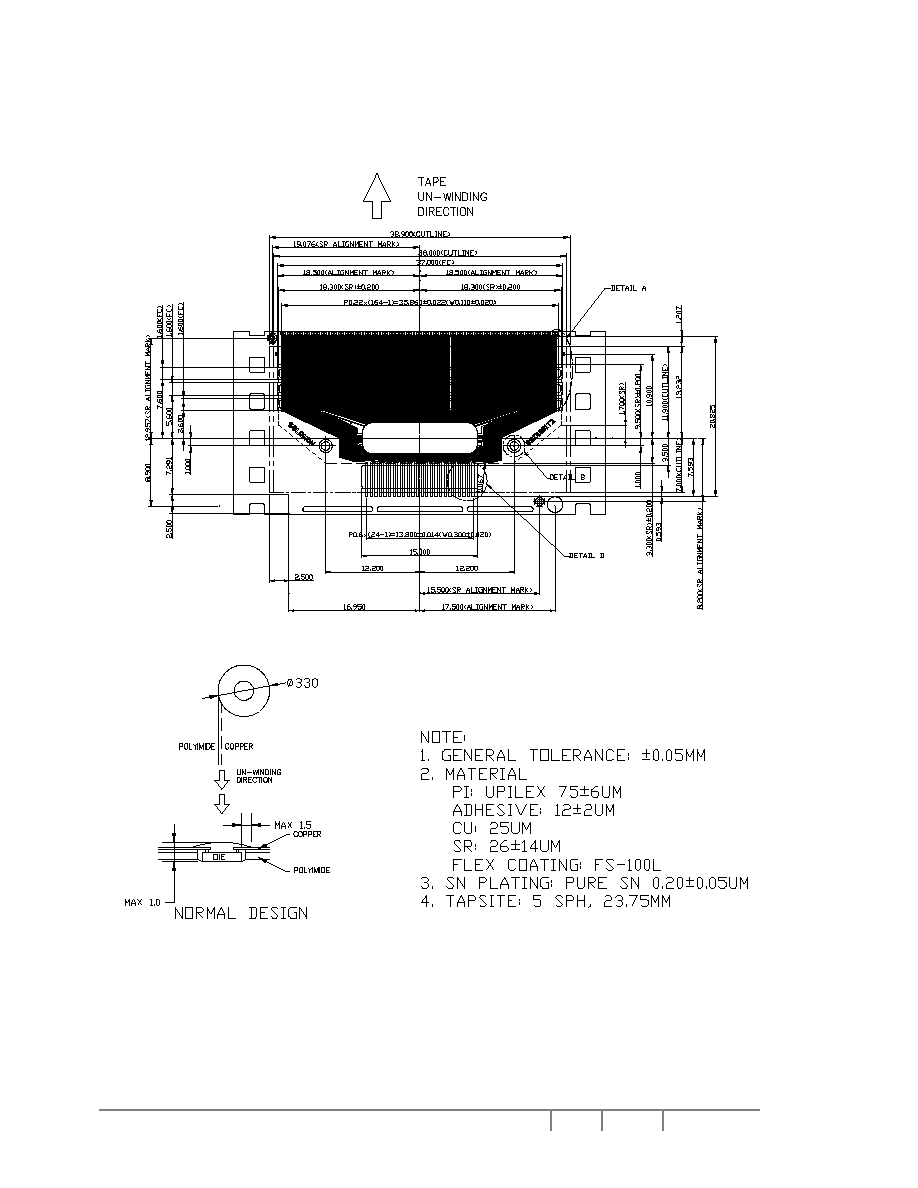
SSD1881T2R TAB PACKAGE DIMENSION ≠ 1
SSD1881
Rev 2.1
P 31
Aug 2003
Solomon Systech
SSD1881T2R TAB PACKAGE DIMENSION ≠ 2

Solomon Systech
Sep 2003
P 32/32 Rev 2.10
SSD1881
http://www.solomon-systech.com
Solomon Systech reserves the right to make changes without further notice to any products herein. Solomon Systech makes no warranty,
representation or guarantee regarding the suitability of its products for any particular purpose, nor does Solomon Systech assume any liability
arising out of the application or use of any product or circuit, and specifically disclaims any and all liability, including without limitation
consequential or incidental damages. "Typical" parameters can and do vary in different applications. All operating parameters, including
"Typicals" must be validated for each customer application by customer's technical experts. Solomon Systech does not convey any license
under its patent rights nor the rights of others. Solomon Systech products are not designed, intended, or authorized for use as components in
systems intended for surgical implant into the body, or other applications intended to support or sustain life, or for any other application in which
the failure of the Solomon Systech product could create a situation where personal injury or death may occur. Should Buyer purchase or use
Solomon Systech products for any such unintended or unauthorized application, Buyer shall indemnify and hold Solomon Systech and its
offices, employees, subsidiaries, affiliates, and distributors harmless against all claims, costs, damages, and expenses, and reasonable
attorney fees arising out of, directly or indirectly, any claim of personal injury or death associated with such unintended or unauthorized use,
even if such claim alleges that Solomon Systech was negligent regarding the design or manufacture of the part.