
TABLE OF CONTENTS
1
GENERAL DESCRIPTION................................................................................................................. 1
2
FEATURES ........................................................................................................................................ 2
2.1
Integrated Display Buffer ......................................................................................................... 2
2.2
Microcontroller Interface.......................................................................................................... 2
2.3
LCD Panel Support ................................................................................................................... 2
2.4
Display Modes........................................................................................................................... 2
2.5
Display Features ....................................................................................................................... 2
2.6
Clock Source ............................................................................................................................. 3
2.7
Miscellaneous............................................................................................................................ 3
2.8
Package...................................................................................................................................... 3
3
ORDERING INFORMATION.............................................................................................................. 3
4
BLOCK DIAGRAM............................................................................................................................. 4
4.1
PIN ARRANGEMENT................................................................................................................. 5
4.1.1
100 pin TQFP ...................................................................................................................... 5
5
PIN DESCRIPTION ............................................................................................................................ 6
5.1
Host Interface ............................................................................................................................ 7
5.2
LCD Interface............................................................................................................................. 9
5.3
Clock Input............................................................................................................................... 10
5.4
Miscellaneous.......................................................................................................................... 10
5.5
Power and Ground .................................................................................................................. 10
5.6
Summary of Configuration Options...................................................................................... 10
5.7
Host Bus Interface Pin Mapping............................................................................................ 11
5.8
LCD Interface Pin Mapping .................................................................................................... 12
5.9
Data Bus Organization ........................................................................................................... 13
6
FUNCTIONAL BLOCK DESCRIPTIONS ........................................................................................ 14

2
6.1
MCU Interface .......................................................................................................................... 14
6.2
Control Register ...................................................................................................................... 14
6.3
Display Output......................................................................................................................... 14
6.4
Display Buffer.......................................................................................................................... 14
6.5
PWM Clock and CV Pulse Control......................................................................................... 14
6.6
Clock Generator ...................................................................................................................... 14
7
REGISTERS ..................................................................................................................................... 15
7.1
Register Mapping.................................................................................................................... 15
7.2
Register Descriptions............................................................................................................. 15
7.2.1
Read-Only Configuration Registers............................................................................... 15
7.2.2
Clock Configuration Registers ....................................................................................... 16
7.2.3
Look-Up Table Registers ................................................................................................ 17
7.2.4
Panel Configuration Registers ....................................................................................... 21
7.2.5
Display Mode Registers .................................................................................................. 31
7.2.6
Floating Window Registers............................................................................................. 36
7.2.7
Miscellaneous Registers................................................................................................. 41
7.2.8
General IO Pins Registers............................................................................................... 43
7.2.9
Pulse Width Modulation (PWM) Clock and Contrast Voltage (CV) Pulse
Configuration Registers................................................................................................................. 46
7.2.10
Cursor Mode Registers ................................................................................................... 49
8
MAXIMUM RATINGS ....................................................................................................................... 60
9
DC CHARACTERISTICS ................................................................................................................. 61
10
AC CHARACTERISTICS ................................................................................................................. 61
10.1
Clock Timing............................................................................................................................ 62
10.1.1
Input Clocks ..................................................................................................................... 62
10.1.2
Internal Clocks ................................................................................................................. 63
10.2
CPU Interface Timing.............................................................................................................. 64
10.2.1
Generic #1 Interface Timing............................................................................................ 64
10.2.2
Generic #2 Interface Timing (e.g. ISA) ........................................................................... 66
10.2.3
Motorola MC68K #1 Interface Timing (e.g. MC68000) .................................................. 68
10.2.4
Motorola DragonBall Interface Timing with DTACK# (e.g. MC68EZ328/MC68VZ328)
70

3
10.2.5
Motorola DragonBall Interface Timing without DTACK# (e.g.
MC68EZ328/MC68VZ328) ............................................................................................................... 72
10.2.6
Hitachi SH-3 Interface Timing (e.g. SH7709A) .............................................................. 74
10.2.7
Hitachi SH-4 Interface Timing (e.g. SH7751) ................................................................. 76
10.3
LCD Power Sequencing ......................................................................................................... 78
10.3.1
Passive/TFT Power-On Sequence.................................................................................. 78
10.3.2
Passive/TFT Power-Off Sequence.................................................................................. 79
10.3.3
Power Saving Status ....................................................................................................... 80
10.4
Display Interface ..................................................................................................................... 81
10.4.1
Generic STN Panel Timing.............................................................................................. 82
10.4.2
Monochrome 4-Bit Panel Timing.................................................................................... 84
10.4.3
Monochrome 8-Bit Panel Timing.................................................................................... 87
10.4.4
Color 4-Bit Panel Timing ................................................................................................. 90
10.4.5
Color 8-Bit Panel Timing (Format stripe) ...................................................................... 93
10.4.6
Generic TFT Panel Timing .............................................................................................. 96
10.4.7
9/12/18-Bit TFT Panel Timing.......................................................................................... 97
10.4.8
160x160 Sharp HR-TFT Panel Timing (e.g. LQ031B1DDxx) ...................................... 101
10.4.9
320x240 Sharp HR-TFT Panel Timing (e.g. LQ039Q2DS01) ...................................... 105
11
CLOCKS......................................................................................................................................... 107
11.1
Clock Descriptions ............................................................................................................... 107
11.1.1
BCLK ............................................................................................................................... 107
11.1.2
MCLK............................................................................................................................... 108
11.1.3
PCLK ............................................................................................................................... 108
11.1.4
PWMCLK.........................................................................................................................109
11.2
Clocks versus Functions ..................................................................................................... 109
12
POWER SAVING MODE................................................................................................................ 110
13
FRAME RATE CALCULATION ..................................................................................................... 110
14
DISPLAY DATA FORMATS .......................................................................................................... 111
15
LOOK-UP TABLE ARCHITECTURE............................................................................................. 112
15.1
Monochrome Modes ............................................................................................................. 112
15.1.1
1 Bit-per-pixel Monochrome Mode............................................................................... 112
15.1.2
2 Bit-per-pixel Monochrome Mode............................................................................... 112

4
15.1.3
4 Bit-per-pixel Monochrome Mode............................................................................... 113
15.1.4
8 Bit-per-pixel Monochrome Mode............................................................................... 113
15.1.5
16 Bit-Per-Pixel Monochrome Mode ............................................................................ 113
15.2
Color Modes .......................................................................................................................... 114
15.2.1
1 Bit-Per-Pixel Color ...................................................................................................... 114
15.2.2
2 Bit-Per-Pixel Color ...................................................................................................... 115
15.2.3
4 Bit-Per-Pixel Color ...................................................................................................... 116
15.2.4
8 Bit-per-pixel Color Mode ............................................................................................ 117
15.2.5
16 Bit-Per-Pixel Color Mode.......................................................................................... 118
16
BIG-ENDIAN BUS INTERFACE .................................................................................................... 118
16.1
Byte Swapping Bus Data...................................................................................................... 118
16.1.1
16 Bpp Color Depth ....................................................................................................... 119
16.1.2
1/2/4/8 Bpp Color Depth ................................................................................................ 119
17
VIRTUAL DISPLAY MODE............................................................................................................ 120
18
DISPLAY ROTATE MODE............................................................................................................. 121
18.1
90� Display Rotate Mode ...................................................................................................... 121
18.1.1
Register Programming .................................................................................................. 121
18.2
180� Display Rotate Mode .................................................................................................... 122
18.2.1
Register Programming .................................................................................................. 122
18.3
270� Display Rotate Mode .................................................................................................... 123
18.3.1
Register Programming .................................................................................................. 123
19
FLOATING WINDOW MODE......................................................................................................... 124
19.1
With Display Rotate Mode Enabled..................................................................................... 125
19.1.1
Display Rotate Mode 90� ............................................................................................... 125
19.1.2
Display Rotate Mode 180� ............................................................................................. 125
19.1.3
Display Rotate Mode 270� ............................................................................................. 126
20
HARDWARE CURSOR MODE...................................................................................................... 127
20.1
With Display Rotate Mode Enabled..................................................................................... 128
20.1.1
Display Rotate Mode 90
�
�
�
� ............................................................................................... 128
20.1.2
Display Rotate Mode 180
�
�
�
� ............................................................................................. 129
20.1.3
Display Rotate Mode 270
�
�
�
� ............................................................................................. 129

5
20.2
Pixel format (Normal orientation mode) ............................................................................. 129
20.2.1
4/8/16 Bit-per-pixel......................................................................................................... 130
20.3
Pixel format (90� Display Rotate Mode) .............................................................................. 130
20.3.1
4 Bit-per-pixel ................................................................................................................. 130
20.3.2
8 Bit-per-pixel ................................................................................................................. 131
20.3.3
16 Bit-per-pixel ............................................................................................................... 131
20.4
Pixel format (180� Display Rotate Mode) ............................................................................ 132
20.4.1
4 Bit-per-pixel ................................................................................................................. 132
20.4.2
8 Bit-per-pixel ................................................................................................................. 132
20.4.3
16 Bit-per-pixel ............................................................................................................... 133
20.5
Pixel format (270� Display Rotate Mode) ............................................................................ 133
20.5.1
4 Bit-per-pixel ................................................................................................................. 133
20.5.2
8 Bit-per-pixel ................................................................................................................. 134
20.5.3
16 Bit-per-pixel ............................................................................................................... 134
21
APPLICATION EXAMPLES .......................................................................................................... 135
22
APPENDIX ..................................................................................................................................... 141
22.1
Package Mechanical Drawing for 100 pins TQFP.............................................................. 141
22.2
Register Table ....................................................................................................................... 142

6
List of Figures
Figure 4-1 : Block Diagram ........................................................................................................................... 4
Figure 4-2 : Pinout Diagram � 100 pin TQFP ............................................................................................... 5
Figure 7-1 : Display Data Byte/Word Swap ................................................................................................ 33
Figure 7-2 : PWM Clock/CV Pulse Block Diagram ..................................................................................... 46
Figure 10-1 : Clock Input Requirements ..................................................................................................... 62
Figure 10-2 : Generic #1 Interface Timing .................................................................................................. 64
Figure 10-3 : Generic #2 Interface Timing .................................................................................................. 66
Figure 10-4 : Motorola MC68K #1 Interface Timing.................................................................................... 68
Figure 10-5 : Motorola DragonBall Interface with DTACK# Timing ............................................................ 70
Figure 10-6 : Motorola DragonBall Interface without DTACK# Timing ....................................................... 72
Figure 10-7 : Hitachi SH-3 Interface Timing................................................................................................ 74
Figure 10-8 : Hitachi SH-4 Interface Timing................................................................................................ 76
Figure 10-9 : Passive/TFT Power-On Sequence Timing ............................................................................ 78
Figure 10-10 : Passive/TFT Power-Off Sequence Timing .......................................................................... 79
Figure 10-11 : Power Saving Status Timing ............................................................................................... 80
Figure 10-12 :
Panel Timing Parameters
................................................................................................ 81
Figure 10-13 :
Generic STN Panel Timing
............................................................................................. 83
Figure 10-14 :
Monochrome 4-Bit Panel Timing
.................................................................................... 84
Figure 10-15 :
Monochrome 4-Bit Panel A.C. Timing
........................................................................... 85
Figure 10-16 :
Monochrome 8-Bit Panel Timing
.................................................................................... 87
Figure 10-17 :
Monochrome 8-Bit Panel A.C. Timing
........................................................................... 88
Figure 10-18 :
Color 4-Bit Panel Timing
.................................................................................................. 90
Figure 10-19 :
Color 4-Bit Panel A.C. Timing
......................................................................................... 91
Figure 10-20 :
Color 8-Bit Panel Timing (Format stripe)
...................................................................... 93
Figure 10-21 :
Color 8-Bit Panel A.C. Timing (Format stripe)
.............................................................. 94
Figure 10-22 :
Generic TFT Panel Timing
.............................................................................................. 96
Figure 10-23 :
12-Bit TFT Panel Timing
.................................................................................................. 97
Figure 10-24 :
TFT A.C. Timing
................................................................................................................ 99
Figure 10-25 :
160x160 Sharp HR-TFT Panel Horizontal Timing
..................................................... 101
Figure 10-26 :
160x160 Sharp HR-TFT Panel Vertical Timing
.......................................................... 103
Figure 10-27 :
320x240 Sharp HR-TFT Panel Horizontal Timing
..................................................... 105
Figure 10-28 :
320x240 Sharp HR-TFT Panel Vertical Timing
.......................................................... 106
Figure 11-1 :
Clock Generator Block Diagram
..................................................................................... 107
Figure 14-1 : 1/2/4/8/16 Bit-Per-Pixel Display Data Memory Organization .............................................. 111
Figure 15-1 :
1 Bit-per-pixel Monochrome Mode Data Output Path
................................................. 112
Figure 15-2 :
2 Bit-per-pixel Monochrome Mode Data Output Path
................................................. 112
Figure 15-3 :
4 Bit-per-pixel Monochrome Mode Data Output Path
................................................. 113
Figure 15-4 :
8 Bit-per-pixel Monochrome Mode Data Output Path
................................................. 113
Figure 15-5 :
1 Bit-Per-Pixel Color Mode Data Output Path
.............................................................. 114
Figure 15-6 :
2 Bit-Per-Pixel Color Mode Data Output Path
.............................................................. 115
Figure 15-7 :
4 Bit-Per-Pixel Color Mode Data Output Path
.............................................................. 116
Figure 15-8 :
8 Bit-per-pixel Color Mode Data Output Path
............................................................... 117
Figure 16-1 :
Byte-swapping for 16 Bpp
............................................................................................... 118
Figure 16-2 :
Byte-swapping for 1/2/4/8 Bpp
....................................................................................... 119
Figure 17-1 : Main Window inside Virtual Image Area.............................................................................. 120
Figure 18-1 : Relationship Between The Screen Image and the Image Refreshed in 90
� Display Rotate
Mode. ................................................................................................................................................. 121
Figure 18-2 : Relationship Between The Screen Image and the Image Refreshed in 180
� Display Rotate
Mode. ................................................................................................................................................. 122

7
Figure 18-3 : Relationship Between The Screen Image and the Image Refreshed in 270
� Display Rotate
Mode. ................................................................................................................................................. 123
Figure 19-1 :
Floating Window with Display Rotate Mode disabled
................................................. 124
Figure 19-2 :
Floating Window with Display Rotate Mode 90� enabled
........................................... 125
Figure 19-3 :
Floating Window with Display Rotate Mode 180� enabled
........................................ 125
Figure 19-4
: Floating Window with Display Rotate Mode 270� enabled
........................................ 126
Figure 20-1 : Display Precedence in Hardware Cursor ............................................................................ 127
Figure 20-2 : Cursors on the main window ............................................................................................... 128
Figure 20-3 : Cursors with Display Rotate Mode 90
� enabled.................................................................. 128
Figure 20-4 : Cursors with Display Rotate Mode 180
� enabled................................................................ 129
Figure 20-5 : Cursors with Display Rotate Mode 270
� enabled................................................................ 129
Figure 21-1: Typical System Diagram (Generic #1 Bus) .......................................................................... 135
Figure 21-2 : Typical System Diagram (Generic #2 Bus) ......................................................................... 136
Figure 21-3 : Typical System Diagram (MC68K # 1, Motorola 16-Bit 68000) .......................................... 137
Figure 21-4 : Typical System Diagram (Motorola MC68EZ328/MC68VZ328 "DragonBall" Bus)............. 138
Figure 21-5 : Typical System Diagram (Hitachi SH-3 Bus)....................................................................... 139
Figure 21-6 : Typical System Diagram (Hitachi SH-4 Bus)....................................................................... 140

8
List of Tables
Table 3-1 : Ordering Information................................................................................................................... 3
Table 4-1 : TQFP Pin Assignment Table ...................................................................................................... 6
Table 5-1 : Host Interface Pin Descriptions .................................................................................................. 7
Table 5-2 :
LCD Interface Pin Descriptions
.............................................................................................. 9
Table 5-3 : Clock Input Pin Descriptions..................................................................................................... 10
Table 5-4 : Miscellaneous Pin Descriptions ................................................................................................ 10
Table 5-5 : Power And Ground Pin Descriptions ........................................................................................ 10
Table 5-6 : Summary of Power-On/Reset Options ..................................................................................... 11
Table 5-7 : Host Bus Interface Pin Mapping ............................................................................................... 11
Table 5-8 : LCD Interface Pin Mapping....................................................................................................... 12
Table 5-9 : Data Bus Organization.............................................................................................................. 13
Table 5-10 : Pin State Summary................................................................................................................. 13
Table 7-1 : MCLK Divide Selection ............................................................................................................. 16
Table 7-2 : PCLK Divide Selection.............................................................................................................. 17
Table 7-3 : PCLK Source Selection ............................................................................................................ 17
Table 7-4 : Panel Data Width Selection ...................................................................................................... 21
Table 7-5 : Active Panel Resolution Selection ............................................................................................ 22
Table 7-6 : LCD Panel Type Selection........................................................................................................ 22
Table 7-7 :
Color Invert Mode Options
.................................................................................................... 32
Table 7-8 :
LCD Bit-per-pixel Selection
.................................................................................................. 33
Table 7-9 : Display Rotate Mode Select Options ........................................................................................ 34
Table 7-10 : 32-bit Address X Increments for Various Color Depths.......................................................... 38
Table 7-11 : 32-bit Address Y Increments for Various Color Depths.......................................................... 39
Table 7-12 : 32-bit Address X Increments for Various Color Depths.......................................................... 40
Table 7-13 : 32-bit Address Y Increments for Various Color Depths.......................................................... 41
Table 7-14 : PWM Clock Control................................................................................................................. 46
Table 7-15 : CV Pulse Control .................................................................................................................... 47
Table 7-16 : PWM Clock Divide Select Options.......................................................................................... 47
Table 7-17 : CV Pulse Divide Select Options ............................................................................................. 48
Table 7-18 : PWM Duty Cycle Select Options ............................................................................................ 49
Table 7-19 : X Increment Mode for Various Color Depths.......................................................................... 52
Table 7-20 : Y Increment Mode for Various Color Depths.......................................................................... 53
Table 8-1 : Absolute Maximum Ratings ...................................................................................................... 60
Table 8-2 : Recommended Operating Conditions ...................................................................................... 60
Table 9-1 : Electrical Characteristics for IOV
DD
= 3.3V typical.................................................................... 61
Table 10-1 : Clock Input Requirements for CLKI ........................................................................................ 62
Table 10-2 : Clock Input Requirements for AUXCLK.................................................................................. 63
Table 10-3 : Internal Clock Requirements .................................................................................................. 63
Table 10-4 : Generic #1 Interface Timing ................................................................................................... 65
Table 10-5 : Generic #2 Interface Timing ................................................................................................... 67
Table 10-6 : Motorola MC68K #1 Interface Timing..................................................................................... 69
Table 10-7 : Motorola DragonBall Interface with DTACK# Timing ............................................................. 71
Table 10-8 : Motorola DragonBall Interface without DTACK# Timing ........................................................ 73
Table 10-9 : Hitachi SH-3 Interface Timing................................................................................................. 75
Table 10-10 : Hitachi SH-4 Interface Timing............................................................................................... 77
Table 10-11 : Passive/TFT Power-On Sequence Timing ........................................................................... 78
Table 10-12 : Passive/TFT Power-Off Sequence Timing ........................................................................... 79
Table 10-13 : Power Saving Status Timing................................................................................................. 80
Table 10-14 : Panel Timing Parameter Definition and Register Summary................................................. 81
Table 10-15 : Monochrome 4-Bit Panel A.C. Timing .................................................................................. 86
Table 10-16 : Monochrome 8-Bit Panel A.C. Timing .................................................................................. 89
Table 10-17 : Color 4-Bit Panel A.C. Timing............................................................................................... 92
Table 10-18 : Color 8-Bit Panel A.C. Timing (Format stripe) ...................................................................... 95

9
Table 10-19 : TFT A.C. Timing.................................................................................................................. 100
Table 10-20 : 160x160 Sharp HR-TFT Horizontal Timing ........................................................................ 102
Table 10-21 : 160x160 Sharp HR-TFT Panel Vertical Timing .................................................................. 104
Table 10-22 : 320x240 Sharp HR-TFT Panel Horizontal Timing .............................................................. 106
Table 10-23 : 320x240 Sharp HR-TFT Panel Vertical Timing .................................................................. 106
Table 11-1 : BCLK Clock Selection........................................................................................................... 107
Table 11-2 : MCLK Clock Selection .......................................................................................................... 108
Table 11-3 : PCLK Clock Selection........................................................................................................... 108
Table 11-4 : Relationship between MCLK and PCLK............................................................................... 109
Table 11-5 :
PWMCLK Clock Selection
................................................................................................ 109
Table 11-6 : SSD1905 Internal Clock Requirements................................................................................ 109
Table 12-1 : Power Saving Mode Function Summary .............................................................................. 110
Table 20-1 : Indexing scheme for Hardware Cursor ................................................................................. 127
Table 22-1 : SSD1905 Register Table (1 of 2).......................................................................................... 142
Table 22-2 : SSD1905 Register Table (2 of 2).......................................................................................... 143


SOLOMON SYSTECH
SEMICONDUCTOR TECHNICAL DATA
This document contains information on a new product. Specifications and information herein are subject to
change without notice.
http://www.solomon-systech.com
SSD1905
Rev 1.4
P 1/144
Oct 2003
Copyright
2003 Solomon Systech Limited
SSD1905
Advance Information
LCD Graphics Controller
CMOS
1 GENERAL
DESCRIPTION
The SSD1905 is a graphics controller with built-in 80Kbyte SRAM display buffer, supporting color and mono LCD.
The SSD1905 can support a wide range of active and passive panels, and interface with various CPUs. The
advanced design, together with integration of memory and timing circuits make a low cost, low power, single chip
solution to meet the handheld devices or appliances market needs, such as Pocket/Palm-size PCs and mobile
communication devices.
The SSD1905 supports most of the resolutions commonly used in portable applications, and is featured with
hardware display rotation, covering different form factor needs. The controller also features Virtual Display,
Floating Window (variable size Overlay Window) and two Cursors to reduce the software manipulation. The 32-bit
internal data path provides high bandwidth display memory for fast screen updates. The SSD1905 also provides
the advantage of a single power supply.
The SSD1905 features low-latency CPU access, which supports microprocessors without READY/WAIT#
handshaking signals. This controller impartiality to CPU type or operating system makes it an ideal display solution
for a wide variety of applications. The SSD1905 is available in a 100 pin TQFP package.

Solomon Systech
Oct 2003 P 2/144
Rev 1.4
SSD1905
2 FEATURES
2.1 Integrated Display Buffer
� Embedded 80K byte SRAM display buffer.
2.2 Microcontroller
Interface
� Directly interfaces to :
Generic #1 bus interface with WAIT# signal
Generic #2 bus interface with WAIT# signal
Motorola MC68K
Motorola MC68EZ328/MC68VZ328/MC68SZ328 DragonBall
Motorola DragonBall MX1 MC9328MX1
Intel StrongARM/ XScale
Hitachi SH-3
Hitachi SH-4
� 8-bit processor support with "glue logic".
� "Fixed" and low-latency CPU access times.
� Registers are memory-mapped with dedicated M/R# input to select between memory and
register address space.
� The contiguous 80K byte display buffer is directly accessible through the 17-bit address bus.
2.3 LCD Panel Support
� 4/8-bit monochrome STN interface.
� 4/8-bit color STN interface.
� 9/12/18-bit Active Matrix TFT interface.
� Direct support for 18-bit Sharp HR-TFT interface (160x160, 320x240).
2.4 Display
Modes
� 1/2/4/8/16 bit-per-pixel (bpp) color depths.
� Up to 64 gray shades using Frame Rate Control (FRC) and dithering on monochrome passive
LCD panels.
� Up to 256k colors on passive STN panels.
� Up to 256k colors on active matrix LCD panels.
� Resolution examples :
320x240 at a color depth of 8 bpp
160x160 at a color depth of 16 bpp
160x240 at a color depth of 16 bpp
2.5 Display
Features
� Display Rotate Mode : 90�, 180�, 270� counter-clockwise hardware rotation of display image.
� Virtual display support : displays image larger than the panel size through the use of panning
and scrolling.
� Floating Window Mode : displays a variable size window overlaid on background image.
� 2 Hardware Cursors (for 4/8/16 bpp) : simultaneously displays two cursors overlaid on
background image.
� Double Buffering/Multi-pages: provides smooth animation and instantaneous screen updates.

SSD1905
Rev 1.4
P 3/144
Oct 2003
Solomon Systech
2.6 Clock
Source
� Two clock inputs: CLKI and AUXCLK. It is possible to use one clock input only.
� Bus clock (BCLK) is derived from CLKI, can be internally divided by 2, 3, or 4.
� Memory clock (MCLK) is derived from BCLK. It can be internally divided by 2, 3, or 4.
� Pixel clock (PCLK) can be derived from CLKI, AUXCLK, BCLK, or MCLK. It can be internally
divided by 2, 3, 4, or 8.
2.7 Miscellaneous
� Hardware/Software Color Invert
� Software Power Saving mode
� General Purpose Input / Output pins available
� Single Supply Operation : 3.0V � 3.6V
2.8 Package
� 100-pin TQFP package
3 ORDERING
INFORMATION
Table 3-1 : Ordering Information
Ordering Part Number
Package Form
SSD1905QT2 100
TQFP
Solomon Systech
Oct 2003 P 4/144
Rev 1.4
SSD1905
4 BLOCK
DIAGRAM
CONT
ROL
RE
GI
S
T
E
R
S
G
P
IO
&
L
O
O
K
U
P
TABL
E (
L
U
T
)
CONT
ROL
RE
GI
S
T
E
R
& GP
I
O
D
I
SPL
A
Y D
A
TA
PR
EFETC
H
U
N
I
T
FR
C
/
TFT C
O
N
T
R
O
LS &
D
I
SPLAY D
A
TA FOR
M
AT
CONV
E
R
T
I
ON
DI
S
P
L
AY
OUT
P
UT
ME
MOR
Y
R
/
W
CONT
ROL
D
I
SPL
AY MEMOR
Y
WI
T
H
CONT
ROL
D
I
SPLA
Y B
U
FFER
(
80K
B
)
READ/WRITE
DECODE
MCU
INTERFACE
M
C
U I
N
T
E
RF
ACE
CLOCK
GE
NE
RA
T
O
R
IN
TER
N
AL
CLOCK
S
G
P
IO
[6
:0
]
GP
O
LFRA
M
E
,
LLI
NE
,
LS
HI
FT,
LDE
N
,
LDA
T
A
[
17:
0]
WE
0#,
WE
1#,
RD/
W
R#,
RD#,
B
S
#,
CS
#;
RE
S
E
T
#
,
M
/
R
#
A
[
16:
0]
D[
15:
0]
C
F
[7
:0
]
WA
I
T
#
C
L
KI, AU
XC
L
K
P
U
LS
E
WI
DT
H M
O
DULA
T
I
ON CLOCK
A
ND
C
O
N
T
R
AST VO
L
T
AG
E PU
L
S
E C
O
N
T
R
O
L
LP
WM
OUT,
LCV
O
UT
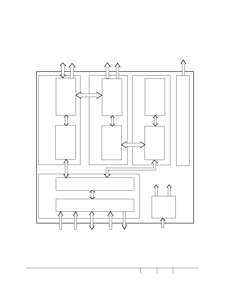
Figure 4-1 : Block Diagram
SSD1905
Rev 1.4
P 5/144
Oct 2003
Solomon Systech
4.1 PIN
ARRANGEMENT
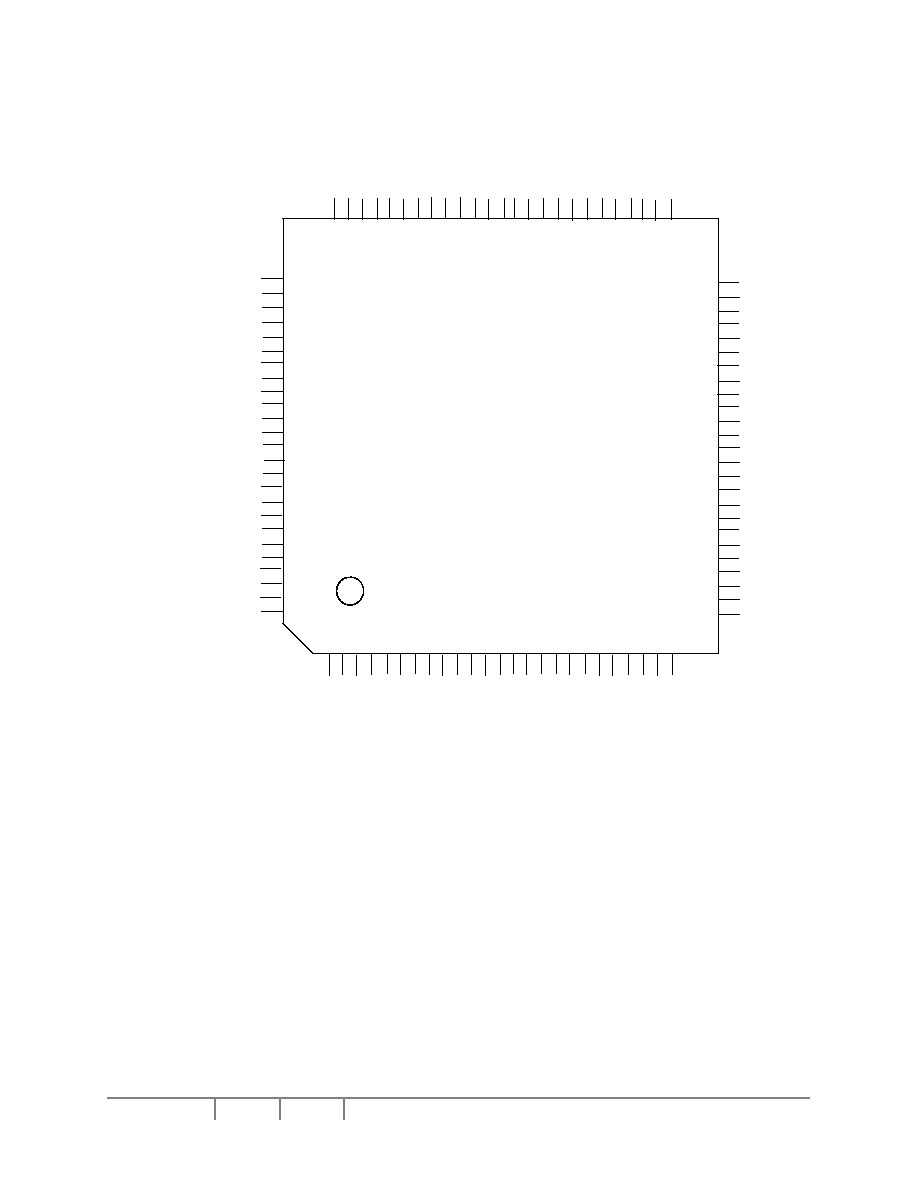
4.1.1 100 pin TQFP
25
24
23
22
21
20
19
18
17
16
15
14
13
12
11
10
9
8
7
6
5
4
3
2
1
VSS
IOVDD
LDEN
CORE
V
D
D
LFRA
M
E
LLI
NE
LSH
I
FT
LDA
T
A
0
LDA
T
A
1
LDA
T
A
2
LDA
T
A
3
LDA
T
A
4
LDA
T
A
5
LDA
T
A
6
VSS
IO
VD
D
LDA
T
A
7
LDA
T
A
8
LDA
T
A
9
LDA
T
A
10
LDA
T
A
11
LDA
T
A
12
LDA
T
A
13
LDA
T
A
14
LDA
T
A
15
LDA
T
A
16
LDA
T
A
17
VSS
50
49
48
47
46
45
44
43
42
41
40
39
38
37
36
35
34
33
32
31
30
29
28
27
26
76
77
78
79
80
81
82
83
84
85
86
87
88
89
90
91
92
93
94
95
96
97
98
99
100
IOVDD
AUXCLK
CF7
CF6
CF5
CF4
CF3
CF2
CF1
CF0
TESTEN
A16
A15
A14
A13
A12
A11
A10
A9
A8
A7
A6
A5
A4
VSS
VSS
D9
D10
D11
D12
D13
D14
D15
WA
I
T
#
IO
VD
D
CLK
I
VSS
R
ESET
#
RD/
W
R
#
WE
1
#
WE
0
#
RD
#
BS
#
M/R
#
CS
#
A0
A1
A2
A3
CORE
V
D
D
SSD1905
GPO
LCVOUT
GPIO0
GPIO1
GPIO2
GPIO3
GPIO4
GPIO5
GPIO6
LPWMOUT
IOVDD
VSS
D0
D1
D2
D3
D4
D5
D6
D7
D8
IOVDD
51
52
53
54
55
56
57
58
59
60
61
62
63
64
65
66
67
68
69
70
71
72
73
74
75
Figure 4-2 : Pinout Diagram � 100 pin TQFP
Note
CoreVDD is an internal regulator output pin. 0.1
�F capacitor to V
SS
must be required on each CoreVDD pin.
Solomon Systech
Oct 2003 P 6/144
Rev 1.4
SSD1905
Table 4-1 : TQFP Pin Assignment Table
Pin #
Signal Name
Pin #
Signal Name
Pin #
Signal Name
Pin #
Signal Name
1 COREVDD 26 IOVDD 51 COREVDD 76
IOVDD
2 A3 27 D8 52
LFRAME
77
AUXCLK
3 A2 28 D7 53
LLINE
78 CF7
4 A1 29 D6 54
LSHIFT
79 CF6
5 A0 30 D5 55
LDATA0
80 CF5
6 CS# 31 D4 56
LDATA
1
81 CF4
7 M/R#
32 D3 57
LDATA
2
82 CF3
8 BS# 33 D2 58
LDATA
3
83 CF2
9 RD# 34 D1 59
LDATA
4
84 CF1
10
WE0#
35 D0 60
LDATA
5
85 CF0
11 WE1# 36 V
SS
61
LDATA
6
86
TESTEN
12 RD/WR# 37 IOVDD 62
V
SS
87 A16
13 RESET# 38
LPWMOUT
63 IOVDD 88 A15
14 V
SS
39
GPIO6
64
LDATA
7
89 A14
15 CLKI 40
GPIO5
65
LDATA
8
90 A13
16 IOVDD 41 GPIO4 66 LDATA
9
91 A12
17 WAIT# 42 GPIO3 67
LDATA
10
92 A11
18 D15 43
GPIO2
68
LDATA
11
93 A10
19 D14 44
GPIO1
69
LDATA
12
94 A9
20 D13 45
GPIO0
70
LDATA
13
95 A8
21 D12 46
LCVOUT
71
LDATA
14
96 A7
22 D11 47 GPO 72
LDATA
15
97 A6
23 D10 48 LDEN 73
LDATA
16
98 A5
24 D9 49
IOVDD
74
LDATA
17
99 A4
25 V
SS
50 V
SS
75 V
SS
100 V
SS
5 PIN
DESCRIPTION
Key:
I = Input
O =Output
IO = Bi-directional (input / output)
P = Power pin
LIS = LVTTL Schmitt input
LB2 = LVTTL IO buffer (8mA/-8mA at 3.3V)
LB3 = LVTTL IO buffer (12mA/-12mA at 3.3V)
LO3 = LVTTL output buffer (12mA/-12mA at 3.3V)
LT2 = Tri-state output buffer (8mA/-8mA at 3.3V)
LT3 = Tri-state output buffer (12mA/-12mA at 3.3V)
Hi-Z = High impedance
Note : LVTTL is low voltage TTL (see Section 9 "DC CHARACTERISTICS").
SSD1905
Rev 1.4
P 7/144
Oct 2003
Solomon Systech
5.1 Host
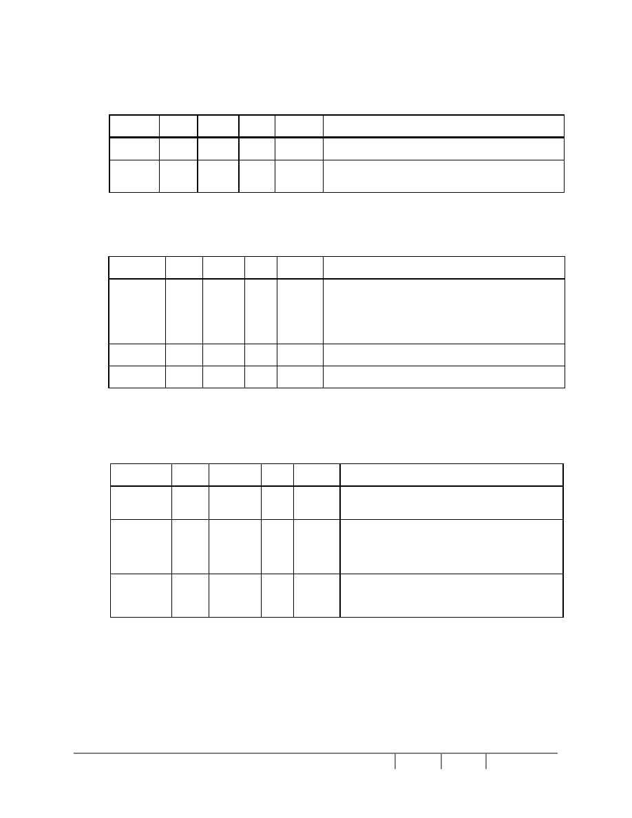
Interface
Table 5-1 : Host Interface Pin Descriptions
Pin Name Type
TQFP
Pin #
Cell
RESET#
State
Description
A0
I
5
LIS
0
This input pin has multiple functions.
� For Generic #1, this pin is not used and should be
connected to V
SS
.
� For Generic #2, this is an input of system address bit 0
(A0).
� For MC68K #1, this is an input of the lower data strobe
(LDS#).
� For DragonBall, this pin is not used and should be
connected to V
SS
.
� For SH-3/SH-4, this pin is not used and should be
connected to VSS.
See Table 5-7 : Host Bus Interface Pin Mapping for summary.
A[16:1] I
2-4, 87-
99
LIS
0
System address bus bits 16-1.
D[15:0] IO
18-24,
27-35
LB2 Hi-Z
Input data from the system data bus.
� For Generic #1, these pins are connected to D[15:0].
� For Generic #2, these pins are connected to D[15:0].
� For MC68K #1, these pins are connected to D[15:0].
� For DragonBall, these pins are connected to D[15:0].
� For SH-3/SH-4, these pins are connected to D[15:0].
See Table 5-7 : Host Bus Interface Pin Mapping for summary.
WE0# I 10 LIS 1
This input pin has multiple functions.
� For Generic #1, this is an input of the write enable signal
for the lower data byte (WE0#).
� For Generic #2, this is an input of the write enable signal
(WE#).
� For MC68K #1, this pin must be tied to IOV
DD
.
� For DragonBall, this is an input of the byte enable signal
for the D[7:0] data byte (LWE#).
� For SH-3/SH-4, this is input of the write enable signal for
data D[7:0].
See Table 5-7 : Host Bus Interface Pin Mapping for summary.
WE1# I 11 LIS 1
This input pin has multiple functions.
� For Generic #1, this is an input of the write enable signal
for the upper data byte (WE1#).
� For Generic #2, this is an input of the byte enable signal
for the high data byte (BHE#).
� For MC68K #1, this is an input of the upper data strobe
(UDS#).
� For DragonBall, this is an input of the byte enable signal
for the D[15:8] data byte (UWE#).
� For SH-3/SH-4, this is input of the write enable signal for
data D[15:8].
See Table 5-7 : Host Bus Interface Pin Mapping for summary.
CS# I 6 LIS 1
Chip select input. See Table 5-7 : Host Bus Interface Pin
Mapping for summary.
M/R# I 7 LIS 0
This input pin is used to select the display buffer or internal
registers of the SSD1905. M/R# is set high to access the
display buffer and low to access the registers.
See Table 5-7 : Host Bus Interface Pin Mapping for summary.

Solomon Systech
Oct 2003 P 8/144
Rev 1.4
SSD1905
Pin Name Type
TQFP
Pin #
Cell
RESET#
State
Description
BS# I 8 LIS 1
This input pin has multiple functions.
� For Generic #1, this pin must be tied to IOV
DD
.
� For Generic #2, this pin must be tied to IOV
DD
.
� For MC68K #1, this is an input of the address strobe
(AS#).
� For DragonBall, this pin must be tied to IOV
DD
.
� For SH-3/SH-4, this is input of the bus start signal (BS#).
See Table 5-7 : Host Bus Interface Pin Mapping for summary.
RD/WR#
I
12
LIS
1
This input pin has multiple functions.
� For Generic #1, this is an input of the read command for
the upper data byte (RD1#).
� For Generic #2, this pin must be tied to IOV
DD
.
� For MC68K #1, this is an input of the R/W# signal.
� For DragonBall, this pin must be tied to IOV
DD
.
� For SH-3/SH-4, this is input of the RD/WR# signal. The
SSD1905 needs this signal for early decode of the bus
cycle.
See Table 5-7 : Host Bus Interface Pin Mapping for summary.
RD#
I
9
LIS
1
This input pin has multiple functions.
� For Generic #1, this is an input of the read command for
the lower data byte (RD0#).
� For Generic #2, this is an input of the read command
(RD#).
� For MC68K #1, this pin must be tied to IOV
DD
.
� For DragonBall, this is an input of the output enable
(OE#).
� For SH-3/SH-4, this is input of the read signal (RD#).
See Table 5-7 : Host Bus Interface Pin Mapping for summary.
WAIT# O 17 LT2 Hi-Z
During a data transfer, this output pin is driven active to force
the system to insert wait states. It is driven inactive to indicate
the completion of a data transfer. WAIT# is released to the
high impedance state after the data transfer is complete. Its
active polarity is configurable. A pull-up or pull-down resistor
should be used to resolve any data contention issues. See
Table 5-6 : Summary of Power-On/Reset Options.
� For Generic #1, this pin outputs the wait signal (WAIT#).
� For Generic #2, this pin outputs the wait signal (WAIT#).
� For MC68K #1, this pin outputs the data transfer
acknowledge signal (DTACK#).
� For DragonBall, this pin outputs the data transfer
acknowledge signal (DTACK#).
� For SH-3 mode, this pin outputs the wait request signal
(WAIT#).
� For SH-4 mode, this pin outputs the device ready signal
(RDY#).
See Table 5-7 : Host Bus Interface Pin Mapping for summary.
RESET# I 13 LIS 0
Active low input to set all internal registers to the default state
and to force all signals to their inactive states. It is
recommended to place a
0.1
�F capacitor to V
SS
.
Note : When reset state is released (RESET# = "H"),
normal operation can be started after 3 BCLK period.

SSD1905
Rev 1.4
P 9/144
Oct 2003
Solomon Systech
5.2 LCD
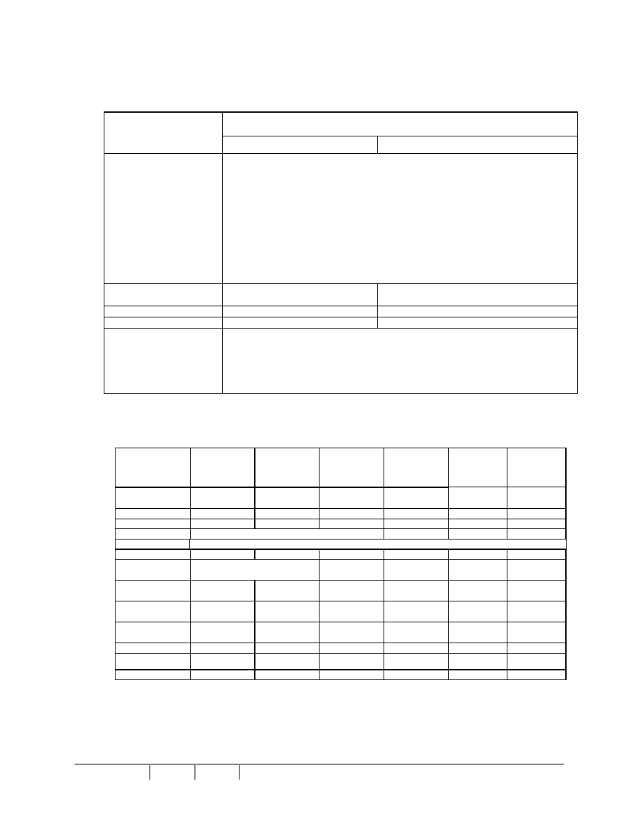
Interface
Table 5-2 :
LCD Interface Pin Descriptions
Pin Name
Type
TQFP
Pin #
Cell
RESET#
State
Description
LDATA[17:0]
O
55-61,
64-74
LO3
0
Panel Data bits 17-0.
LFRAME O 52 LO3 0
This output pin has multiple functions.
� Frame Pulse
� SPS for Sharp HR-TFT
See Table 5-8 : LCD Interface Pin Mapping for summary.
LLINE O 53 LO3 0
This output pin has multiple functions.
� Line Pulse
� LP for Sharp HR-TFT
See Table 5-8 : LCD Interface Pin Mapping for summary.
LSHIFT O 54 LO3 0
This output pin has multiple functions.
� Shift Clock
� CLK for Sharp HR-TFT
See Table 5-8 : LCD Interface Pin Mapping for summary.
LDEN O 48
LO3 0
This output pin has multiple functions.
� Display enable (LDEN) for TFT panels
� LCD backplane bias signal (MOD) for all other LCD
panels
See Table 5-8 : LCD Interface Pin Mapping for summary.
GPIO0 IO 45
LIS/
LT3
0
This pin has multiple functions.
� PS for Sharp HR-TFT
� General purpose IO pin 0 (GPIO0)
� Hardware Color Invert
See Table 5-8 : LCD Interface Pin Mapping for summary.
GPIO1 IO 44 LB3 0
This pin has multiple functions.
� CLS for Sharp HR-TFT
� General purpose IO pin 1 (GPIO1)
See Table 5-8 : LCD Interface Pin Mapping for summary.
GPIO2 IO 43 LB3 0
This pin has multiple functions.
� REV for Sharp HR-TFT
� General purpose IO pin 2 (GPIO2)
See Table 5-8 : LCD Interface Pin Mapping for summary.
GPIO3 IO 42 LB3 0
This pin has multiple functions.
� SPL for Sharp HR-TFT
� General purpose IO pin 3 (GPIO3)
See Table 5-8 : LCD Interface Pin Mapping for summary.
GPIO4 IO 41 LB3 0
This pin has multiple functions.
� General purpose IO pin 4 (GPIO4)
See Table 5-8 : LCD Interface Pin Mapping for summary.
GPIO5 IO 40 LB3 0
This pin has multiple functions.
� General purpose IO pin 5 (GPIO5)
See Table 5-8 : LCD Interface Pin Mapping for summary.
GPIO6 IO 39 LB3 0
This pin has multiple functions.
� General purpose IO pin 6 (GPIO6)
See Table 5-8 : LCD Interface Pin Mapping for summary.
LPWMOUT O 38 LB3
0
This output pin has multiple functions.
� PWM Clock output
� General purpose output
LCVOUT O 46 LB3 0
This output pin has multiple functions.
� CV Pulse Output
� General purpose output
Solomon Systech
Oct 2003 P 10/144
Rev 1.4
SSD1905
5.3 Clock
Input
Table 5-3 : Clock Input Pin Descriptions
Pin Name Type
TQFP
Pin #
Cell
RESET#
State
Description
CLKI
I
15
LIS
--
Typically used as input clock source for bus clock and
memory clock
AUXCLK I 77 LIS --
This pin may be used as input clock source for pixel
clock. This input pin must be connected to V
SS
if not
used.
5.4 Miscellaneous
Table 5-4 : Miscellaneous Pin Descriptions
Pin Name Type
TQFP
Pin #
Cell
RESET
# State
Description
CF[7:0] I 78-85
LIS --
These inputs are used to configure the SSD1905 � see
Table 5-6 : Summary of Power-On/Reset Options.
Note: These pins are used for configuration of the
SSD1905 and must be connected directly to IOV
DD
or V
SS
.
GPO O 47
LO3 0
General Purpose Output (possibly used for controlling
the LCD power).
TESTEN I 86 LIS --
Test Enable input used for production test only and
should be tied to V
SS
.
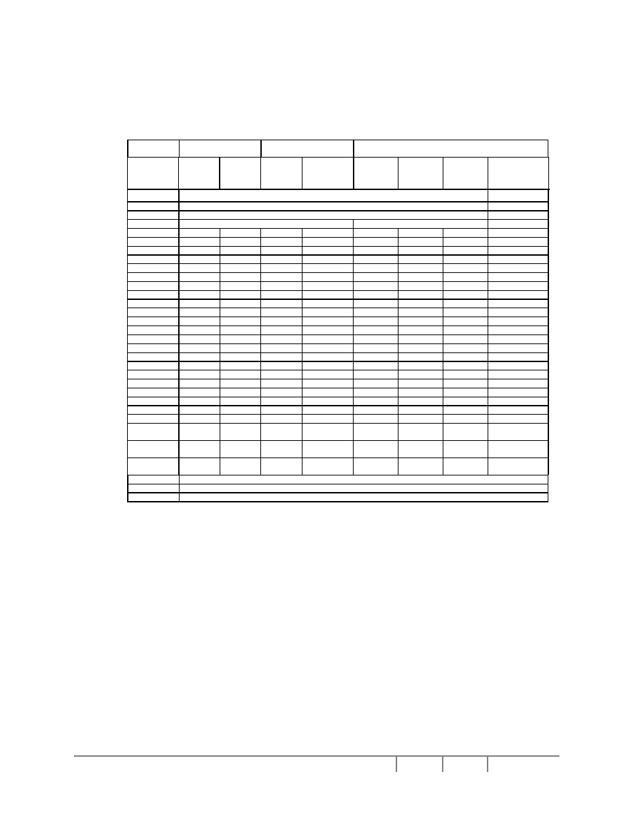
5.5 Power and Ground
Table 5-5 : Power And Ground Pin Descriptions
Pin Name
Type
TQFP
Pin #
Cell
RESET
# State
Description
IOV
DD
P
16, 26,
37, 49,
63, 76
P --
Power supply pins. It is recommended to place a
0.1
�F bypass capacitor close to each of these pins.
COREV
DD
P 1,
51 P --
COREV
DD
pins are internal voltage regulator output
pins that is used by the internal circuitry only. They
cannot be used for driving external circuitry.
It is required to place a 0.1
�F bypass capacitor
close to each of these pins.
V
SS
P
14, 25,
36, 50,
62, 75,
100
P --
Ground pins
5.6 Summary of Configuration Options
These pins are used for configuration of the SSD1905 and must be connected directly to IOV
DD
or V
SS
. The state
of CF[5:0] is latched on the rising edge of RESET# or after the software reset function is activated (REG[A2h] bit
0). Changing state at any other time has no effect.
SSD1905
Rev 1.4
P 11/144 Oct 2003
Solomon Systech
Table 5-6 : Summary of Power-On/Reset Options
Power-On/Reset State
SSD1905
Configuration
Input
1 (Connected to IOV
DD
)
0 (Connected to V
SS
)
CF[2:0]
Select host bus interface as follows:
CF2 CF1 CF0 Host
Bus
0 0 0 SH-3/SH-4
0 0 1 MC68K
#1
0 1 0 Reserved
0 1 1 Generic#1
1 0 0 Generic#2
1 0 1 Reserved
1 1 0 DragonBall
(MC68EZ328/MC68VZ328)
1 1 1 Reserved
Note: The host bus interface is 16-bit only.
CF3
Configure GPIO pins as inputs at
power-on
Configure GPIO pins as outputs at power-on
(for use by HR-TFT when selected)
CF4
Big Endian bus interface
Little Endian bus interface
CF5
WAIT# is active high
WAIT# is active low
CF[7:6]
CLKI to BCLK divide select:
CF7 CF6 CLKI to BCLK Divide Ratio
0 0 1:1
0 1 2:1
1 0 3:1
1 1 4:1
5.7 Host Bus Interface Pin Mapping
Table 5-7 : Host Bus Interface Pin Mapping
SSD1905 Pin
Name
Generic #1
Generic #2
Motorola
MC68K #1
Motorola
MC68EZ328/
MC68VZ328
DragonBall
Hitachi
SH-3
Hitachi
SH-4
A0
Connected to
V
SS
A0 LDS#
Connected to
V
SS
Connected to
VSS
Connected to
VSS
A[16:1] A[16:1] A[16:1] A[16:1] A[16:1] A[16:1]
A[16:1]
D[15:0] D[15:0]
D[15:0]
D[15:0]
1
D[15:0] D[15:0] D[15:0]
CS# External
Decode
CSX#
CSn#
CSn#
M/R# External
Decode
CLKI BUSCLK
BUSCLK CLK CLKO CKIO
CKIO
BS#
Connected to IOV
DD
AS#
Connected to
IOV
DD
BS# BS#
RD/WR# RD1#
Connected to
IOV
DD
R/W#
Connected to
IOV
DD
RD/WR# RD/WR#
RD# RD0#
RD#
Connected to
IOV
DD
OE# RD# RD#
WE0# WE0# WE#
Connected to
IOV
DD
LWE# WE0# WE0#
WE1# WE1# BHE# UDS#
UWE#
WE1#
WE1#
WAIT# WAIT#
WAIT#
DTACK#
DTACK#
WAIT#
RDY#
RESET# RESET# RESET# RESET# RESET# RESET#
RESET#
Note
1
If the target MC68K bus is 32-bit, then these signals should be connected to D[31:16].
Solomon Systech
Oct 2003 P 12/144
Rev 1.4
SSD1905
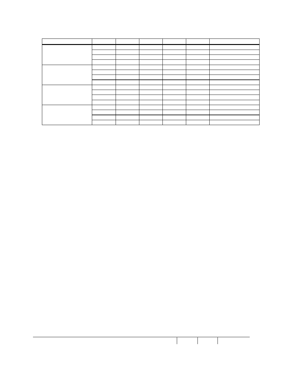
5.8
LCD Interface Pin Mapping
Table 5-8 : LCD Interface Pin Mapping
Pin Name
Monochrome
Passive Panel
Color Passive Panel
Color TFT Panel
4-bit
8-bit
4-bit
8-bit
9-bit
12-bit
18-bit
18-bit Sharp
(format
stripe)
HR-TFT
1
LFRAME
LFRAME
SPS
LLINE
LLINE
LP
LSHIFT LSHIFT
CLK
LDEN MOD
LDEN
no
connect
LDATA0
Drive 0
D0
Drive 0
D0(G3)
2
R2 R3 R5 R5
LDATA1
Drive 0
D1
Drive 0
D1(R3)
2
R1 R2 R4 R4
LDATA2
Drive 0
D2
Drive 0
D2(B2)
2
R0 R1 R3 R3
LDATA3
Drive 0
D3
Drive 0
D3(G2)
2
G2 G3 G5 G5
LDATA4 D0 D4
D0(R2)
2
D4(R2)
2
G1 G2 G4 G4
LDATA5 D1 D5
D1(B1)
2
D5(B1)
2
G0 G1 G3 G3
LDATA6 D2 D6
D2(G1)
2
D6(G1)
2
B2 B3 B5 B5
LDATA7 D3 D7
D3(R1)
2
D7(R1)
2
B1 B2 B4 B4
LDATA8
Drive 0
Drive 0
Drive 0
Drive 0
B0
B1
B3
B3
LDATA9
Drive 0
Drive 0
Drive 0
Drive 0
Drive 0
R0
R2
R2
LDATA10
Drive 0
Drive 0
Drive 0
Drive 0
Drive 0
Drive 0
R1
R1
LDATA11
Drive 0
Drive 0
Drive 0
Drive 0
Drive 0
Drive 0
R0
R0
LDATA12
Drive 0
Drive 0
Drive 0
Drive 0
Drive 0
G0
G2
G2
LDATA13
Drive 0
Drive 0
Drive 0
Drive 0
Drive 0
Drive 0
G1
G1
LDATA14
Drive 0
Drive 0
Drive 0
Drive 0
Drive 0
Drive 0
G0
G0
LDATA15
Drive 0
Drive 0
Drive 0
Drive 0
Drive 0
B0
B2
B2
LDATA16
Drive 0
Drive 0
Drive 0
Drive 0
Drive 0
Drive 0
B1
B1
LDATA17
Drive 0
Drive 0
Drive 0
Drive 0
Drive 0
Drive 0
B0
B0
GPIO0 GPIO0 GPIO0 GPIO0 GPIO0 GPIO0 GPIO0 GPIO0
PS
GPIO1 GPIO1 GPIO1 GPIO1 GPIO1 GPIO1 GPIO1 GPIO1
CLS
GPIO2 GPIO2 GPIO2 GPIO2 GPIO2 GPIO2 GPIO2 GPIO2
REV
GPIO3 GPIO3 GPIO3 GPIO3 GPIO3 GPIO3 GPIO3 GPIO3
SPL
GPIO4 GPIO4 GPIO4 GPIO4 GPIO4 GPIO4 GPIO4 GPIO4
GPIO4
(output only)
GPIO5 GPIO5 GPIO5 GPIO5 GPIO5 GPIO5 GPIO5 GPIO5
GPIO5
(output only)
GPIO6 GPIO6 GPIO6 GPIO6 GPIO6 GPIO6 GPIO6 GPIO6
GPIO6
(output only)
GPO
GPO (General Purpose Output)
LCVOUT LCVOUT
LPWMOUT LPWMOUT
Note
1
GPIO pins must be configured as outputs (CF3 = 0 during RESET# active) when HR-TFT panels are selected.
2
These pin mappings use signal names commonly used for each panel type, however signal names may differ
between panel manufacturers. The values shown in brackets represent the color components as mapped to the
corresponding LDATAxx signals at the first valid edge of LSHIFT. For further LDATAxx to LCD interface
mapping, see Section 10.4 "Display Interface".

SSD1905
Rev 1.4
P 13/144 Oct 2003
Solomon Systech
5.9 Data Bus Organization
There are two data bus architectures, little endian and big endian. Little endian means the bytes at lower
addresses have lower significance. Big endian means the most significant byte has the lowest address.
Table 5-9 : Data Bus Organization
D[15:8]
D[7:0]
Big endian
2N
2N + 1
Little endian
2N + 1
2N
N : Byte Address
Table 5-10 : Pin State Summary
MCU Mode (Endian)
A0 RD/WR# RD# WE1# WE0#
Operation
X 0 0 1 1
Word
read
X
0
1
1
1
High byte read 2N
X
1
0
1
1
Low byte read 2N+1
X 1 1 0 0
Word
write
X
1
1
0
1
High byte write 2N
Generic#1 (Big)
X
1
1
1
0
Low byte write 2N+1
X 0 0 1 1
Word
read
X
0
1
1
1
High byte read 2N+1
X
1
0
1
1
Low byte read 2N
X 1 1 0 0
Word
write
X
1
1
0
1
High byte write 2N+1
Generic#1 (Little)
X
1
1
1
0
Low byte write 2N
0 X 0 0 1
Word
read
0
X
0
1
1
High byte read 2N
1
X
0
0
1
Low byte read 2N+1
0 X 1 0 0
Word
write
0
X
1
1
0
High byte write 2N
Generic#2 (Big)
1
X
1
0
0
Low byte write 2N+1
0 X 0 0 1
Word
read
1
X
0
0
1
High byte read 2N+1
0
X
0
1
1
Low byte read 2N
0 X 1 0 0
Word
write
1
X
1
0
0
High byte write 2N+1
Generic#2 (Little)
0
X
1
1
0
Low byte write 2N
0 1 X 0 X
Word
read
1
1
X
0
X
High byte read 2N
0
1
X
1
X
Low byte read 2N+1
0 0 X 0 X
Word
write
1
0
X
0
X
High byte write 2N
MC68K#1 (Big)
0
0
X
1
X
Low byte write 2N+1
0 1 X 0 X
Word
read
0
1
X
1
X
High byte read 2N+1
1
1
X
0
X
Low byte read 2N
0 0 X 0 X
Word
write
0
0
X
1
X
High byte write 2N+1
MC68K#1 (Little)
1
0
X
0
X
Low byte write 2N
Solomon Systech
Oct 2003 P 14/144
Rev 1.4
SSD1905
MCU Mode (Endian)
A0 RD/WR# RD# WE1# WE0#
Operation
X X 0 X X
Word
read
X X 1 0 0
Word
write
X
X
1
0
1
High byte write 2N
MC68EZ328 /
MC68VZ328 (Big)
X
X
1
1
0
Low byte write 2N+1
X X 0 X X
Word
read
X X 1 0 0
Word
write
X
X
1
0
1
High byte write 2N+1
MC68EZ328 /
MC68VZ328 (Little)
X
X
1
1
0
Low byte write 2N
X X 0 1 1
Word
read
X X 1 0 0
Word
write
X
X
1
0
1
High byte write 2N
SH-3/SH-4 (Big)
X
X
1
1
0
Low byte write 2N+1
X X 0 1 1
Word
read
X X 1 0 0
Word
write
X
X
1
0
1
High byte write 2N+1
SH-3/SH-4 (Little)
X
X
1
1
0
Low byte write 2N
6 FUNCTIONAL BLOCK DESCRIPTIONS
6.1 MCU
Interface
Responds to bus request for various kinds of MCU and translates to internal interface signals.
6.2 Control
Register
The control register stores register data to control the LCD panel. The register data is through the MCU Interface
read/write to control the register value. The read/write access of LUT is also controlled by the control register. The
detail of this register and register mapping will be discussed in Section 7 "Registers".
6.3 Display
Output
Display output serializes the display data from display buffer and reconstructs the data according to the display
panel format. When the display mode is not 16 bpp, display data will be converted to color data by the built-in 18
bit LUT. For details about LUT, please refer to Section 15 "Look-Up Table Architecture".
6.4 Display
Buffer
Display buffer consists of 80KB SRAM, which is organized as a 32-bit wide internal data path for fast display data
retrieval.
6.5 PWM Clock and CV Pulse Control
Provides programmable waveform for Pulse Width Modulation (PWM) and Contrast Voltage (CV) generation.
6.6 Clock
Generator
Clock Generator provides internal clocks. For detail operation of clock generator, please refer to Section 11
"Clocks".

SSD1905
Rev 1.4
P 15/144 Oct 2003
Solomon Systech
7 Registers
This section discusses how and where to access the SSD1905 registers. It also provides detailed information
about the layout and usage of each register.
7.1 Register
Mapping
The SSD1905 registers are memory-mapped. When the system decodes the input pins as CS# = 0 and M/R# = 0,
the registers may be accessed. The register space is decoded by A[16:0].
7.2 Register
Descriptions
Unless specified otherwise, all register bits are set to 0 during power-on or software reset (REG[A2h] bit 0 = 1). All
bits marked "0" should be programmed as zero. All bits marked "1" should be programmed as one.
Key :
RO : Read Only
WO : Write Only
RW : Read / Write
NA : Not Applicable
X : Don't care
7.2.1 Read-Only Configuration Registers
Display Buffer Size Register
REG[01h]
Bit
7 6 5 4 3 2 1 0
Display
Buffer
Size
Bit 7
Display
Buffer
Size
Bit 6
Display
Buffer
Size
Bit 5
Display
Buffer
Size
Bit 4
Display
Buffer
Size
Bit 3
Display
Buffer
Size
Bit 2
Display
Buffer
Size
Bit 1
Display
Buffer
Size
Bit 0
Type
RO RO RO RO RO RO RO RO
Reset
state
0 0 0 1 0 1 0 0
Bits 7-0
Display Buffer Size Bits [7:0]
This register indicates the size of the SRAM display buffer in 4K byte multiple. The
SSD1905 display buffer is 80K bytes and therefore this register returns a value of 20
(14h).
Value of this register
= display buffer size
� 4K bytes
= 80K bytes
� 4K bytes
= 20 (14h)
Configuration Readback Register
REG[02h]
Bit
7 6 5 4 3 2 1 0
CF7
Status
CF6 Status
CF5 Status
CF4 Status
CF3 Status
CF2 Status
CF1 Status
CF0 Status
Type
RO RO RO RO RO RO RO RO
Reset
state
X X X X X X X X
Bits 7-0
CF[7:0] Status
These status bits return the status of the configuration pins CF[7:0]. CF[5:0] are
latched at the rising edge of RESET# or software reset (REG[A2h] bit 0 = 1).
Solomon Systech
Oct 2003 P 16/144
Rev 1.4
SSD1905
Product / Revision Code Register
REG[03h]
Bit
7 6 5 4 3 2 1 0
Product
Code
Bit 5
Product
Code
Bit 4
Product
Code
Bit 3
Product
Code
Bit 2
Product
Code
Bit 1
Product
Code
Bit 0
Revision
Code Bit 1
Revision
Code Bit 0
Type
RO RO RO RO RO RO RO RO
Reset
state
0 0 0 1 0 1 X X
Bits 7-2
Product Code Bits [5:0]
These bits indicate the product code. The product code of SSD1905 is 000101.
Bits 1-0
Revision Code Bits [1:0]
These are read-only bits that indicate the revision code.
7.2.2 Clock Configuration Registers
Memory Clock Configuration Register
REG[04h]
Bit
7 6 5 4 3 2 1 0
0
0
MCLK
Divide
Select Bit 1
MCLK
Divide
Select Bit 0
0
0
0
0
Type
NA
NA
RW RW NA
NA
NA
NA
Reset
state
0 0 0 0 0 0 0 0
Bits 5-4
MCLK Divide Select Bits [1:0]
These bits determine the divide used to generate the Memory Clock (MCLK) from the
Bus Clock (BCLK).
Table 7-1 : MCLK Divide Selection
MCLK Divide Select Bits [1:0]
BCLK to MCLK Frequency Ratio
00 1:1
01 2:1
10 3:1
11 4:1
Pixel Clock Configuration Register
REG[05h]
Bit
7 6 5 4 3 2 1 0
0
PCLK
Divide
Select Bit 2
PCLK
Divide
Select Bit 1
PCLK
Divide
Select Bit 0
0
0
PCLK
Source
Select Bit 1
PCLK
Source
Select Bit 0
Type
NA
RW RW RW NA
NA
RW RW
Reset
state
0 0 0 0 0 0 0 0
Bits 6-4
PCLK Divide Select Bits [2:0]
These bits determine the divided used to generate the Pixel Clock (PCLK) from the
Pixel Clock Source.

SSD1905
Rev 1.4
P 17/144 Oct 2003
Solomon Systech
Table 7-2 : PCLK Divide Selection
PCLK Divide Select Bits [2:0]
PCLK Source to PCLK Frequency Ratio
000 1:1
001 2:1
010 3:1
011 4:1
1XX 8:1
x = don't care
Bits 1-0
PCLK Source Select Bits [1:0]
These bits determine the source of the Pixel Clock (PCLK).
Table 7-3 : PCLK Source Selection
PCLK Source Select Bits [1:0]
PCLK Source
00 MCLK
01 BCLK
10 CLKI
11 AUXCLK
7.2.3 Look-Up Table Registers
Look-Up Table Blue Write Data Register
REG[08h]
Bit
7 6 5 4 3 2 1 0
LUT
Blue
Write Data
Bit 5
LUT Blue
Write Data
Bit 4
LUT Blue
Write Data
Bit 3
LUT Blue
Write Data
Bit 2
LUT Blue
Write Data
Bit 1
LUT Blue
Write Data
Bit 0
X
X
Type
WO WO WO WO WO WO WO
WO
Reset
state
0 0 0 0 0 0 0 0
Bits 7-2
LUT Blue Write Data Bits [5:0]
This register contains the data to be written to the blue component of the Look-Up
Table.
The data is stored in this register until a write to the LUT Write Address register
(REG[0Bh]) moves the data into the Look-Up Table.
Note
The LUT entry is updated only when the LUT Write Address Register (REG[0Bh]) is
written.

Solomon Systech
Oct 2003 P 18/144
Rev 1.4
SSD1905
Look-Up Table Green Write Data Register
REG[09h]
Bit
7 6 5 4 3 2 1 0
LUT
Green
Write Data
Bit 5
LUT Green
Write Data
Bit 4
LUT Green
Write Data
Bit 3
LUT Green
Write Data
Bit 2
LUT Green
Write Data
Bit 1
LUT Green
Write Data
Bit 0
X
X
Type
WO WO WO WO WO WO WO
WO
Reset
state
0 0 0 0 0 0 0 0
Bits 7-2
LUT Green Write Data Bits [5:0]
This register contains the data to be written to the green component of the Look-Up
Table.
The data is stored in this register until a write to the LUT Write Address register
(REG[0Bh]) moves the data into the Look-Up Table.
Note
The LUT entry is updated only when the LUT Write Address Register (REG[0Bh]) is
written.
Look-Up Table Red Write Data Register
REG[0Ah]
Bit
7 6 5 4 3 2 1 0
LUT
Red
Write Data
Bit 5
LUT Red
Write Data
Bit 4
LUT Red
Write Data
Bit 3
LUT Red
Write Data
Bit 2
LUT Red
Write Data
Bit 1
LUT Red
Write Data
Bit 0
X
X
Type
WO WO WO WO WO WO WO
WO
Reset
state
0 0 0 0 0 0 0 0
Bits 7-2
LUT Red Write Data Bits [5:0]
This register contains the data to be written to the red component of the Look-Up
Table.
The data is stored in this register until a write to the LUT Write Address register
(REG[0Bh]) moves the data into the Look-Up Table.
Note
The LUT entry is updated only when the LUT Write Address Register (REG[0Bh]) is
written.

SSD1905
Rev 1.4
P 19/144 Oct 2003
Solomon Systech
Look-Up Table Write Address Register
REG[0Bh]
Bit
7 6 5 4 3 2 1 0
LUT
Write
Address Bit
7
LUT Write
Address Bit
6
LUT Write
Address Bit
5
LUT Write
Address Bit
4
LUT Write
Address Bit
3
LUT Write
Address Bit
2
LUT Write
Address Bit
1
LUT Write
Address Bit
0
Type
WO WO WO WO WO WO WO WO
Reset
state
0 0 0 0 0 0 0 0
Bits 7-0
LUT Write Address Bits [7:0]
This register is a pointer to the Look-Up Table (LUT) which is used to write LUT data
stored in REG[08h], REG[09h], and REG[0Ah]. The data is updated to the LUT only
with the completion of a write to this register. This is a write-only register and
returns 00h if read.
Note
The SSD1905 has three 256-entry, 6-bit-wide LUTs, one for each of red, green and
blue (see Section 15 "Look-Up Table Architecture").
Look-Up Table Blue Read Data Register
REG[0Ch]
Bit
7 6 5 4 3 2 1 0
LUT
Blue
Read Data
Bit 5
LUT Blue
Read Data
Bit 4
LUT Blue
Read Data
Bit 3
LUT Blue
Read Data
Bit 2
LUT Blue
Read Data
Bit 1
LUT Blue
Read Data
Bit 0
0
0
Type
RO RO RO RO RO RO RO
RO
Reset
state
0 0 0 0 0 0 0 0
Bits 7-2
LUT Blue Read Data Bits [5:0]
This register contains the data from the blue component of the Look-Up Table. The
LUT entry read is controlled by the LUT Read Address Register (REG[0Fh]).
Note
This register is updated only when the LUT Read Address Register (REG[0Fh]) is
written.
Look-Up Table Green Read Data Register
REG[0Dh]
Bit
7 6 5 4 3 2 1 0
LUT
Green
Read Data
Bit 5
LUT Green
Read Data
Bit 4
LUT Green
Read Data
Bit 3
LUT Green
Read Data
Bit 2
LUT Green
Read Data
Bit 1
LUT Green
Read Data
Bit 0
0
0
Type
RO RO RO RO RO RO RO
RO
Reset
state
0 0 0 0 0 0 0 0
Bits 7-2
LUT Green Read Data Bits [5:0]
This register contains the data from the green component of the Look-Up Table. The
LUT entry read is controlled by the LUT Read Address Register (REG[0Fh]).
Note
This register is updated only when the LUT Read Address Register (REG[0Fh]) is
written.

Solomon Systech
Oct 2003 P 20/144
Rev 1.4
SSD1905
Look-Up Table Red Read Data Register
REG[0Eh]
Bit
7 6 5 4 3 2 1 0
LUT
Red
Read Data
Bit 5
LUT Red
Read Data
Bit 4
LUT Red
Read Data
Bit 3
LUT Red
Read Data
Bit 2
LUT Red
Read Data
Bit 1
LUT Red
Read Data
Bit 0
0
0
Type
RO RO RO RO RO RO RO
RO
Reset
state
0 0 0 0 0 0 0 0
Bits 7-2
LUT Red Read Data Bits [5:0]
This register contains the data from the red component of the Look-Up Table. The LUT
entry read is controlled by the LUT Read Address Register (REG[0Fh]).
Note
This register is updated only when the LUT Read Address Register (REG[0Fh]) is
written.
Look-Up Table Read Address Register
REG[0Fh]
Bit
7 6 5 4 3 2 1 0
LUT
Read
Address Bit
7
LUT Read
Address Bit
6
LUT Read
Address Bit
5
LUT Read
Address Bit
4
LUT Read
Address Bit
3
LUT Read
Address Bit
2
LUT Read
Address Bit
1
LUT Read
Address Bit
0
Type
WO WO WO WO WO WO WO WO
Reset
state
0 0 0 0 0 0 0 0
Bits 7-0
LUT Read Address Bits [7:0]
This register is a pointer to the Look-Up Table (LUT) which is used to read LUT data
and store it in REG[0Ch], REG[0Dh], REG[0Eh]. The data is read from the LUT only
when a write to this register is completed. This is a write-only register and returns
00h if read.
Note
The SSD1905 has three 256-entry, 6-bit-wide LUTs, one for each of red, green and
blue (see Section 15 "Look-Up Table Architecture").

SSD1905
Rev 1.4
P 21/144 Oct 2003
Solomon Systech
7.2.4 Panel Configuration Registers
Panel Type Register
REG[10h]
Bit
7 6 5 4 3 2 1 0
Color STN
Panel
Select
Color/Mono
Panel
Select
Panel Data
Width Bit 1
Panel Data
Width Bit 0
Active
Panel
Resolution
Select
0
Panel Type
Bit 1
Panel Type
Bit 0
Type
RW RW RW RW RW NA RW RW
Reset
state
0 0 0 0 0 0 0 0
Bit 7
Color STN Panel Select
When this bit = 0, non color STN LCD panel is selected.
When this bit = 1, color STN LCD panel is selected.
Bit 6
Color/Mono Panel Select
When this bit = 0, monochrome LCD panel is selected.
When this bit = 1, color LCD panel is selected.
Bits 5-4
Panel Data Width Bits [1:0]
These bits are determined by the data width of the LCD panel. Refer to Table 7-4 :
Panel Data Width Selection for the selection.
Table 7-4 : Panel Data Width Selection
Panel Data Width Bits [1:0]
Passive Panel Data Width
Active Panel Data Width
00 4-bit 9-bit
01 8-bit 12-bit
10 Reserved 18-bit
11 Reserved Reserved
Bit 3
Active Panel Resolution Select
This bit determines one of two panel resolutions when HR-TFT is selected.
This bit has no effect unless HR-TFT is selected (REG[10h] bits 1:0 = 10).
Note
This bit sets some internal non-configurable timing values for the selected panel.
However, all panel configuration registers (REG[12h] � REG[40h]) still require
programming with the appropriate values for the selected panel.
For panel AC timing, see Section 10.4 "Display Interface".

Solomon Systech
Oct 2003 P 22/144
Rev 1.4
SSD1905
Table 7-5 : Active Panel Resolution Selection
Active Panel Resolution Select Bit
HR-TFT Resolution
0 160x160
1 320x240
Bits 1-0
Panel Type Bits[1:0]
These bits select the panel type.
Table 7-6 : LCD Panel Type Selection
Panel Type Bits [1:0]
Panel Type
00 STN
01 TFT
10 HR-TFT
11 Reserved
MOD Rate Register
REG[11h]
Bit
7 6 5 4 3 2 1 0
0
0
MOD Rate
Bit 5
MOD Rate
Bit 4
MOD Rate
Bit 3
MOD Rate
Bit 2
MOD Rate
Bit 1
MOD Rate
Bit 0
Type
NA
NA
RW RW RW RW RW RW
Reset
state
0
0
0 0 0 0 0 0
Bits 5-0
MOD Rate Bits [5:0]
When these bits are all 0, the MOD output signal (LDEN) toggles every LFRAME.
For any non-zero value n, the MOD output signal (LDEN) toggles every n LLINE.
These bits are for passive LCD panels only.
Horizontal Total Register
REG[12h]
Bit
7 6 5 4 3 2 1 0
0
Horizontal
Total Bit 6
Horizontal
Total Bit 5
Horizontal
Total Bit 4
Horizontal
Total Bit 3
Horizontal
Total Bit 2
Horizontal
Total Bit 1
Horizontal
Total Bit 0
Type
NA
RW RW RW RW RW RW RW
Reset
state
0 0 0 0 0 0 0 0
Bits 6-0
Horizontal Total Bits [6:0]
These bits specify the LCD panel Horizontal Total period, in 8 pixel resolution. The
Horizontal Total is the sum of the Horizontal Display period and the Horizontal Non-
Display period. The maximum Horizontal Total is 1024 pixels. See Figure 10-12 :
Panel Timing Parameters
.
Horizontal Total in number of pixels = (Bits [6:0] + 1) x 8
Note
This register must be programmed such that the following condition is fulfilled.
HDPS + HDP < HT
For panel AC timing and timing parameter definitions, see Section 10.4 "Display
Interface".

SSD1905
Rev 1.4
P 23/144 Oct 2003
Solomon Systech
Horizontal Display Period Register
REG[14h]
Bit
7 6 5 4 3 2 1 0
0
Horizontal
Display
Period Bit 6
Horizontal
Display
Period Bit 5
Horizontal
Display
Period Bit 4
Horizontal
Display
Period Bit 3
Horizontal
Display
Period Bit 2
Horizontal
Display
Period Bit 1
Horizontal
Display
Period Bit 0
Type
NA
RW RW RW RW RW RW RW
Reset
state
0 0 0 0 0 0 0 0
Bits 6-0
Horizontal Display Period Bits [6:0]
These bits specify the LCD panel Horizontal Display period, in 8 pixel resolution. The
Horizontal Display period should be less than the Horizontal Total to allow for a
sufficient Horizontal Non-Display period.
Horizontal Display Period in number of pixels = (Bits [6:0] + 1) x 8
Note
Maximum value of REG[14h]
0x3F when Display Rotate Mode (90� or 270�) is
selected.
For panel AC timing and timing parameter definitions, see Section 10.4 "Display
Interface".
Horizontal Display Period Start Position Register 0
REG[16h]
Bit
7 6 5 4 3 2 1 0
Horizontal
Display
Period Start
Position Bit
7
Horizontal
Display
Period Start
Position Bit
6
Horizontal
Display
Period Start
Position Bit
5
Horizontal
Display
Period Start
Position Bit
4
Horizontal
Display
Period Start
Position Bit
3
Horizontal
Display
Period Start
Position Bit
2
Horizontal
Display
Period Start
Position Bit
1
Horizontal
Display
Period Start
Position Bit
0
Type
RW
RW RW RW RW RW RW RW
Reset
state
0 0 0 0 0 0 0 0
Horizontal Display Period Start Position Register 1
REG[17h]
Bit
7 6 5 4 3 2 1 0
0
0
0
0
0
0
Horizontal
Display
Period Start
Position Bit
9
Horizontal
Display
Period Start
Position Bit
8
Type
NA
NA
NA
NA
NA
NA
RW RW
Reset
state
0 0 0 0 0 0 0 0
REG[17h] bits1-0,
REG[16h] bits 7-0
Horizontal Display Period Start Position Bits [9:0]
These bits specify the Horizontal Display Period Start Position in 1 pixel resolution.
Note
For panel AC timing and timing parameter definitions, see Section 10.4 "Display
Interface".
Vertical Total Register 0
REG[18h]
Bit
7 6 5 4 3 2 1 0
Vertical
Total Bit 7
Vertical
Total Bit 6
Vertical
Total Bit 5
Vertical
Total Bit 4
Vertical
Total Bit 3
Vertical
Total Bit 2
Vertical
Total Bit 1
Vertical
Total Bit 0
Type
RW
RW RW RW RW RW RW RW
Reset
state
0 0 0 0 0 0 0 0

Solomon Systech
Oct 2003 P 24/144
Rev 1.4
SSD1905
Vertical Total Register 1
REG[19h]
Bit
7 6 5 4 3 2 1 0
0
0
0
0
0
0
Vertical
Total Bit 9
Vertical
Total Bit 8
Type
NA
NA
NA
NA
NA
NA
RW RW
Reset
state
0 0 0 0 0 0 0 0
REG[19h] bits 1-0,
REG[18h] bits 7-0
Vertical Total Bits [9:0]
These bits specify the LCD panel Vertical Total period, in 1 line resolution. The Vertical
Total is the sum of the Vertical Display Period and the Vertical Non-Display Period.
The maximum Vertical Total is 1024 lines. See Figure 10-12 :
Panel Timing
Parameters
.
Vertical Total in number of lines = Bits [9:0]+ 1
Note
This register must be programmed such that the following condition is fulfilled.
For passive LCD interface : VDPS + VDP + 1 < VT
For other LCD interface : VDPS + VDP < VT
For panel AC timing and timing parameter definitions, see Section 10.4 "Display
Interface".
Vertical Display Period Register 0
REG[1Ch]
Bit
7 6 5 4 3 2 1 0
Vertical
Display
Period Bit 7
Vertical
Display
Period Bit 6
Vertical
Display
Period Bit 5
Vertical
Display
Period Bit 4
Vertical
Display
Period Bit 3
Vertical
Display
Period Bit 2
Vertical
Display
Period Bit 1
Vertical
Display
Period Bit 0
Type
RW
RW RW RW RW RW RW RW
Reset
state
0 0 0 0 0 0 0 0
Vertical Display Period Register 1
REG[1Dh]
Bit
7 6 5 4 3 2 1 0
0
0
0
0
0
0
Vertical
Display
Period Bit 9
Vertical
Display
Period Bit 8
Type
NA
NA
NA
NA
NA
NA
RW RW
Reset
state
0 0 0 0 0 0 0 0
REG[1Dh] bits 1-0,
REG[1Ch] bits 7-0
Vertical Display Period Bits [9:0]
These bits specify the LCD panel Vertical Display period, in 1 line resolution. The
Vertical Display period should be less than the Vertical Total to allow for a sufficient
Vertical Non-Display period.
Vertical Display Period in number of lines = Bits [9:0] + 1
Note
For panel AC timing and timing parameter definitions, see Section 10.4 "Display
Interface".

SSD1905
Rev 1.4
P 25/144 Oct 2003
Solomon Systech
Vertical Display Period Start Position Register 0
REG[1Eh]
Bit
7 6 5 4 3 2 1 0
Vertical
Display
Period Start
Position Bit
7
Vertical
Display
Period Start
Position Bit
6
Vertical
Display
Period Start
Position Bit
5
Vertical
Display
Period Start
Position Bit
4
Vertical
Display
Period Start
Position Bit
3
Vertical
Display
Period Start
Position Bit
2
Vertical
Display
Period Start
Position Bit
1
Vertical
Display
Period Start
Position Bit
0
Type
RW
RW RW RW RW RW RW RW
Reset
state
0 0 0 0 0 0 0 0
Vertical Display Period Start Position Register 1
REG[1Fh]
Bit
7 6 5 4 3 2 1 0
0
0
0
0
0
0
Vertical
Display
Start
Position
Period Bit 9
Vertical
Display
Start
Position
Period Bit 8
Type
NA
NA
NA
NA
NA
NA
RW RW
Reset
state
0 0 0 0 0 0 0 0
REG[1Fh] bits 1-0,
REG[1Eh] bits 7-0
Vertical Display Period Start Position Bits [9:0]
These bits specify the Vertical Display Period Start Position in 1 line resolution.
Note
For panel AC timing and timing parameter definitions, see Section 10.4 "Display
Interface".
LLINE Pulse Width Register
REG[20h]
Bit
7 6 5 4 3 2 1 0
LLINE
Pulse
Polarity
LLINE
Pulse Width
Bit 6
LLINE
Pulse Width
Bit 5
LLINE
Pulse Width
Bit 4
LLINE
Pulse Width
Bit 3
LLINE
Pulse Width
Bit 2
LLINE
Pulse Width
Bit 1
LLINE
Pulse Width
Bit 0
Type
RW
RW RW RW RW RW RW RW
Reset
state
0 0 0 0 0 0 0 0
Bit 7
LLINE Pulse Polarity
This bit determines the polarity of the horizontal sync signal. The horizontal sync signal
is typically named as LLINE or LP, depending on the panel type.
When this bit = 0, the horizontal sync signal is active low.
When this bit = 1, the horizontal sync signal is active high.
Bits 6-0
LLINE Pulse Width Bits [6:0]
These bits specify the width of the panel horizontal sync signal, in number of PCLK.
The horizontal sync signal is typically named as LLINE or LP, depending on the panel
type.
LLINE Pulse Width in PCLK = Bits [6:0] + 1
Note
For panel AC timing and timing parameter definitions, see Section 10.4 "Display Interface".

Solomon Systech
Oct 2003 P 26/144
Rev 1.4
SSD1905
LLINE Pulse Start Position Register 0
REG[22h]
Bit
7 6 5 4 3 2 1 0
LLINE
Pulse Start
Position Bit
7
LLINE
Pulse Start
Position Bit
6
LLINE
Pulse Start
Position Bit
5
LLINE
Pulse Start
Position Bit
4
LLINE
Pulse Start
Position Bit
3
LLINE
Pulse Start
Position Bit
2
LLINE
Pulse Start
Position Bit
1
LLINE
Pulse Start
Position Bit
0
Type
RW
RW RW RW RW RW RW RW
Reset
state
0 0 0 0 0 0 0 0
LLINE Pulse Start Position Register 1
REG[23h]
Bit
7 6 5 4 3 2 1 0
0
0
0
0
0
0
LLINE
Pulse Start
Position Bit
9
LLINE
Pulse Start
Position Bit
8
Type
NA
NA
NA
NA
NA
NA
RW RW
Reset
state
0 0 0 0 0 0 0 0
REG[23h] bits 1-0,
REG[22h] bits 7-0
LLINE Pulse Start Position Bits [9:0]
These bits specify the start position of the horizontal sync signal, in number of PCLK.
The maximum allowed value of LLINE Pulse Start Position Bits is 3FEh.
LLINE Pulses Start Position in PCLK = Bits [9:0] + 1
Note
For panel AC timing and timing parameter definitions, see Section10.4 "Display Interface".
LFRAME Pulse Width Register
REG[24h]
Bit
7 6 5 4 3 2 1 0
LFRAME
Pulse
Polarity
0
0
0
0
LFRAME
Pulse Width
Bit 2
LFRAME
Pulse Width
Bit 1
LFRAME
Pulse Width
Bit 0
Type
RW
NA
NA
NA
NA
RW RW RW
Reset
state
0 0 0 0 0 0 0 0
Bit 7
LFRAME Pulse Polarity
This bit selects the polarity of the vertical sync signal. The vertical sync signal is
typically named as LFRAME or SPS, depending on the panel typeWhen this bit = 0,
the vertical sync signal is active low.
When this bit = 1, the vertical sync signal is active high.
Bits 2-0
LFRAME Pulse Width Bits [2:0]
These bits specify the width of the panel vertical sync signal, in 1 line resolution. The
vertical sync signal is typically named as LFRAME or SPS, depending on the panel
type. The maximum allowed value of LFRAME Pulse Width Bits is 6.
LFRAME Pulse Width in number of pixels = (Bits [2:0] + 1) x Horizontal Total + offset
Note
For panel AC timing and timing parameter definitions, see Section 10.4 "Display Interface".

SSD1905
Rev 1.4
P 27/144 Oct 2003
Solomon Systech
LFRAME Pulse Start Position Register 0
REG[26h]
Bit
7 6 5 4 3 2 1 0
LFRAME
Pulse Start
Position Bit
7
LFRAME
Pulse Start
Position Bit
6
LFRAME
Pulse Start
Position Bit
5
LFRAME
Pulse Start
Position Bit
4
LFRAME
Pulse Start
Position Bit
3
LFRAME
Pulse Start
Position Bit
2
LFRAME
Pulse Start
Position Bit
1
LFRAME
Pulse Start
Position Bit
0
Type
RW
RW RW RW RW RW RW RW
Reset
state
0 0 0 0 0 0 0 0
LFRAME Pulse Start Position register 1
REG[27h]
Bit
7 6 5 4 3 2 1 0
0
0
0
0
0
0
LFRAME
Pulse Start
Position Bit
9
LFRAME
Pulse Start
Position Bit
8
Type
NA
NA
NA
NA
NA
NA
RW RW
Reset
state
0 0 0 0 0 0 0 0
REG[27h] bits 1-0
REG[26h] bits 7-0
LFRAME Pulse Start Position Bits [9:0]
These bits specify the start position of the vertical sync signal, in 1 line resolution.
LFRAME Pulse Start Position in number of pixels = (Bits [9:0]) x Horizontal Total +
offset
Note
For panel AC timing and timing parameter definitions, see Section 10.4 "Display Interface".
LFRAME Pulse Start Offset Register 0
REG[30h]
Bit
7 6 5 4 3 2 1 0
LFRAME
Start Offset
Bit 7
LFRAME
Start Offset
Bit 6
LFRAME
Start Offset
Bit 5
LFRAME
Start Offset
Bit 4
LFRAME
Start Offset
Bit 3
LFRAME
Start Offset
Bit 2
LFRAME
Start Offset
Bit 1
LFRAME
Start Offset
Bit 0
Type
RW
RW RW RW RW RW RW RW
Reset
state
0 0 0 0 0 0 0 0
LFRAME Pulse Start Offset Register 1
REG[31h]
Bit
7 6 5 4 3 2 1 0
0
0
0
0
0
0
LFRAME
Start Offset
Bit 9
LFRAME
Start Offset
Bit 8
Type
NA
NA
NA
NA
NA
NA
RW RW
Reset
state
0 0 0 0 0 0 0 0
REG[31h] bits 1-0
REG[30h] bits 7-0
LFRAME Pulse Start Offset [9:0]
These bits specify the start offset of the vertical sync signal within a line, in 1 pixel
resolution.
Note
For panel AC timing and timing parameter definitions, see Section 10.4 "Display Interface".

Solomon Systech
Oct 2003 P 28/144
Rev 1.4
SSD1905
LFRAME Pulse Stop Offset Register 0
REG[34h]
Bit
7 6 5 4 3 2 1 0
LFRAME
Stop Offset
Bit 7
LFRAME
Stop Offset
Bit 6
LFRAME
Stop Offset
Bit 5
LFRAME
Stop Offset
Bit 4
LFRAME
Stop Offset
Bit 3
LFRAME
Stop Offset
Bit 2
LFRAME
Stop Offset
Bit 1
LFRAME
Stop Offset
Bit 0
Type
RW
RW RW RW RW RW RW RW
Reset
state
0 0 0 0 0 0 0 0
LFRAME Pulse Stop Offset Register 1
REG[35h]
Bit
7 6 5 4 3 2 1 0
0
0
0
0
0
0
LFRAME
Stop Offset
Bit 9
LFRAME
Stop Offset
Bit 8
Type
NA
NA
NA
NA
NA
NA
RW RW
Reset
state
0 0 0 0 0 0 0 0
REG[35h] bits 1-0
REG[34h] bits 7-0
LFRAME Pulse Stop Offset [9:0]
These bits specify the stop offset of the vertical sync signal within a line, in 1 pixel
resolution.
Note
For panel AC timing and timing parameter definitions, see Section 10.4 "Display Interface".
HR-TFT Special Output Register
REG[38h]
Bit
7 6 5 4 3 2 1 0
0
0
GPIO
Preset
Enable
LSHIFT
Polarity
swap
LSHIFT
Mask
GPIO0 /
GPIO1
Swap
PS
Alternate
CLS Double
Type
NA
NA
RW
RW
RW
RW
RW RW
Reset
state
0 0 0 0 0 0 0 0
Bit 5
GPIO Preset Enable
When this bit = 1, GPIO1 can be toggled once per line, GPIO0 and GPIO2 signals
should be programmed with the appropriate values with REG[3Ch], [3Eh] and [40h].
When this bit = 0, GPIO0, GPIO1 and GPIO2 signals are preset to defined values.
Bit 4
LSHIFT Polarity Swap
When this bit = 1, LSHIFT signal is falling trigger.
When this bit = 0, LSHIFT signal is rising trigger.
Bit 3
LSHIFT Mask
When this bit = 1, LSHIFT signal is enabled in non display period.
When this bit = 0, LSHIFT signal is masked in non display period.
Bit 2
GPIO0 / GPIO1 Swap
When this bit = 1, GPIO0 / GPIO1 signals are swapped.
When this bit = 0, GPIO0 / GPIO1 signals are not swapped.
Bit 1
PS Alternate
When this bit = 1, PS signal change alternatively.
When this bit = 0, PS signal remain the same.
Bit 0
CLS Double
When this bit = 1, number of CLS pulse remain the same.
When this bit = 0, number of CLS pulse will be doubled.
Note
Bit 5 is effective for 320x240 HR-TFT panels only (REG[10h] bit 3 = 1, REG[10h] bits 1-0 =
10).

SSD1905
Rev 1.4
P 29/144 Oct 2003
Solomon Systech
If bit 4 is set to 1, LSHIFT pin will be driven high at power saving mode.
Bits 4-2 are effective for HR-TFT panels only (REG[10h] bits 1-0 = 10).
Bits 1-0 are effective for 160x160 HR-TFT panels only (REG[10h] bit 3 = 0 and REG[10h]
bits 1-0 = 10).
For panel AC timing and timing parameter definitions, see Section 10.4.8 "160x160 Sharp
HR-TFT Panel Timing (e.g. LQ031B1DDxx)" and 10.4.9 "320x240 Sharp HR-TFT Panel
Timing (e.g. LQ039Q2DS01)".
GPIO0 Pulse Start Register
REG[3Ch]
Bit
7 6 5 4 3 2 1 0
GPIO0
Start Bit 7
GPIO0
Start Bit 6
GPIO0
Start Bit 5
GPIO0
Start Bit 4
GPIO0
Start Bit 3
GPIO0
Start Bit 2
GPIO0
Start Bit 1
GPIO0
Start Bit 0
Type
RW
RW RW RW RW RW RW RW
Reset
state
0 0 0 0 0 0 0 0
Bits 7-0
GPIO0 Pulse Start [7:0]
These bits specify the start offset of the GPIO0 signal within a line, in 1 pixel resolution.
Note
This register is effective for 320x240 HR-TFT panels and GPIO Preset enabled only
(REG[10h] bit 3 = 1, REG[10h] bits 1-0 = 10 and REG[38h] bit 5 = 1).
For panel AC timing and timing parameter definitions, see Section 10.4.9 "320x240 Sharp
HR-TFT Panel Timing (e.g. LQ039Q2DS01)".
GPIO0 Pulse Stop Register
REG[3Eh]
Bit
7 6 5 4 3 2 1 0
GPIO0
Stop
Bit 7
GPIO0 Stop
Bit 6
GPIO0 Stop
Bit 5
GPIO0 Stop
Bit 4
GPIO0 Stop
Bit 3
GPIO0 Stop
Bit 2
GPIO0 Stop
Bit 1
GPIO0 Stop
Bit 0
Type
RW
RW RW RW RW RW RW RW
Reset
state
0 0 0 0 0 0 0 0
Bits 7-0
GPIO0 Pulse Stop [7:0]
These bits specify the stop offset of the GPIO0 signal within a line, in 1 pixel resolution.
Note
This register is effective for 320x240 HR-TFT panels and GPIO Preset enabled only
(REG[10h] bit 3 = 1, REG[10h] bits 1-0 = 10 and REG[38h] bit 5 = 1).
For panel AC timing and timing parameter definitions, see Section 10.4.9 "320x240 Sharp
HR-TFT Panel Timing (e.g. LQ039Q2DS01)".

Solomon Systech
Oct 2003 P 30/144
Rev 1.4
SSD1905
GPIO2 Pulse Delay Register
REG[40h]
Bit
7 6 5 4 3 2 1 0
GPIO2
Delay Bit 7
GPIO2
Delay Bit 6
GPIO2
Delay Bit 5
GPIO2
Delay Bit 4
GPIO2
Delay Bit 3
GPIO2
Delay Bit 2
GPIO2
Delay Bit 1
GPIO2
Delay Bit 0
Type
RW
RW RW RW RW RW RW RW
Reset
state
0 0 0 0 0 0 0 0
Bits 7-0
GPIO2 Pulse Delay [7:0]
These bits specify the pulse delay of the GPIO2 signal within a line, in 1 pixel
resolution.
Note
This register is effective for 320x240 HR-TFT panels and GPIO Preset enabled only
(REG[10h] bit 3 = 1, REG[10h] bits 1-0 = 10 and REG[38h] bit 5 = 1).
For panel AC timing and timing parameter definitions, see Section 10.4.9 "320x240 Sharp
HR-TFT Panel Timing (e.g. LQ039Q2DS01)".
STN Color Depth Control Register
REG[45h]
Bit
7 6 5 4 3 2 1 0
0
0
0
0
0
0
0
STN Color
Depth
Control
Type
NA
NA
NA
NA
NA
NA
NA
RW
Reset
state
0 0 0 0 0 0 0 0
Bit 0
STN Color Depth control
This bit controls the maximum number of color available for STN panels.
When this bit = 0, it allows maximum 32k color depth.
When this bit = 1, it allows maximum 256k color depth.
Please refer to Table 7-8 :
LCD Bit-per-pixel Selection
for the color depth
relationship.
Note
REG[45h] is effective for STN panel only (REG[10h] bits 1:0 = 00).

SSD1905
Rev 1.4
P 31/144 Oct 2003
Solomon Systech
Dynamic Dithering Control Register
REG[50h]
Bit
7 6 5 4 3 2 1 0
Dynamic
Dithering
Enable
0
0
0
0
0
0
1
Type
RW
NA
NA
NA
NA
NA
NA
RO
Reset
state
0 0 0 0 0 0 0 1
Bit 7
Dynamic Dithering Enable
This bit will enable the dynamic dithering, the dithering mask will change after each 16
frames.
When this bit = 0, dynamic dithering is disabled.
When this bit = 1, dynamic dithering is enabled.
Note
REG[45h] is effective for both STN panel and dithering enabled (REG[10h] bits 1:0 =
00 and REG[70h] bit 6 = 0).
7.2.5 Display Mode Registers
Display Mode Register
REG[70h]
Bit
7 6 5 4 3 2 1 0
Display
Blank
Dithering
Disable
Hardware
Color Invert
Enable
Software
Color Invert
0
Bit-per-pixel
Select Bit 2
Bit-per-pixel
Select Bit 1
Bit-per-pixel
Select Bit 0
Type
RW
RW
RW
RW
NA
RW
RW
RW
Reset
state
0 0 0 0 0 0 0 0
Bit 7
Display Blank
When this bit = 0, the LCD display output is enabled.
When this bit = 1, the LCD display output is blank and all LCD data outputs are forced
to zero (i.e., the screen is blanked).
Bit 6
Dithering Disable
SSD1905 use a combination of FRC and 4 pixel square formation dithering to achieve
more colors per pixel.
When this bit = 0, dithering is enabled on the passive LCD panel. It allows maximum
64 intensity levels for each color component (RGB).
When this bit = 1, dithering is disabled on the passive LCD panel. It allows maximum
16 intensity levels for each color component (RGB).
Note
This bit does not refer to the number of simultaneously displayed colors but rather the
maximum available colors (refer Table 7-8 : LCD Bit-per-pixel Selection for the
maximum number of displayed colors).
Solomon Systech
Oct 2003 P 32/144
Rev 1.4
SSD1905
Bit 5
Hardware Color Invert Enable
This bit allows the Color Invert feature to be controlled using the General Purpose IO
pin GPIO0. This bit has no effect if REG[70h] bit 7 = 1. This option is not available if
configured for a HR-TFT as GPIO0 is used as an LCD control signal.
When this bit = 0, GPIO0 has no effect on the display color.
When this bit = 1, display color may be inverted via GPIO0.
Note
Display color is inverted after the Look-Up Table.
The SSD1905 requires some configurations before the hardware color invert feature
enabled.
� CF3 must be set to 1 during RESET# is active
� GPIO Pin Input Enable (REG[A9h] bit 7) must be set to 1
� GPIO0 Pin IO Configuration (REG[A8h] bit 0) must be set to 0
If Hardware Color Invert is not available (i.e. HR-TFT panel is used), the color invert
function can be controlled by software using REG[70h] bit 4. Table 7-7 :
Color Invert
Mode Options
summarizes the color invert options available.
Bit 4
Software Color Invert
When this bit = 0, display color is normal.
When this bit = 1, display color is inverted.
See Table 7-7 : Color Invert Mode Options. This bit has no effect if REG[70h] bit 7 = 1
or REG[70h] bit 5 = 1.
Note
Display color is inverted after the Look-Up Table.
Table 7-7 :
Color Invert Mode Options
Hardware Color Invert Enable
Software Color Invert
GPIO0
Display Color
0 0
X
Normal
0 1
X
Invert
1 X
0
Normal
1 X
1
Invert
x = don't care
Bits 2-0
Bit-per-pixel Select Bits [2:0]
These bits select the color depth (bit-per-pixel) for the displayed data for both the main
window and the floating window (if active).
Note
1, 2, 4 and 8 bpp modes use the 18-bit LUT, allowing maximum 256K colors. 16 bpp
mode bypasses the LUT, allowing 64K colors.
SSD1905
Rev 1.4
P 33/144 Oct 2003
Solomon Systech
Table 7-8 :
LCD Bit-per-pixel Selection
Maximum Number of Colors/Shades
Passive Panel
(Dithering On)
Bit-per-pixel
Select Bits [2:0]
Color Depth
(bpp)
REG[45h]
bit 0 = 0
REG[45h]
bit 0 = 1
TFT Panel
Max. No. Of
Simultaneously
Displayed
Colors/Shades
000 1
bpp
32K/32
256K/64
256K/64
2/2
001 2
bpp
32K/32
256K/64
256K/64
4/4
010 4
bpp
32K/32
256K/64
256K/64
16/16
011 8
bpp
32K/32
256K/64
256K/64
256/64
100
16
bpp
32K/32 64K/64 64K/64
64K/64
101, 110, 111
Reserved
n/a
n/a
n/a
n/a
Special Effects Register
REG[71h]
Bit
7 6 5 4 3 2 1 0
Display
Data
Word Swap
Display
Data
Byte Swap
0
Floating
Window
Enable
0
0
Display
Rotate
Mode
Select
Bit 1
Display
Rotate
Mode
Select
Bit 0
Type
RW
RW
NA
RW
NA
NA
RW
RW
Reset
state
0 0 0 0 0 0 0 0
Bit 7
Display Data Word Swap
The display pipe fetches 32-bit of data from the display buffer. This bit enables the
lower 16-bit word and the upper 16-bit word to be swapped before sending them to the
LCD display. If the Display Data Byte Swap bit is also enabled, then the byte order of
the fetched 32-bit data is reversed.
Bit 6
Display Data Byte Swap
The display pipe fetches 32-bit of data from the display buffer. This bit enables
swapping of byte 0 and byte 1, byte 2 and byte 3, before sending them to the LCD. If
the Display Data Word Swap bit is also set, then the byte order of the fetched 32-bit
data is reversed.
Note
For further information on byte swapping for Big Endian mode, see Section 16 "Big-Endian
Bus Interface".
Data
Serialization
32-bit display data
from display buffer
Word Swap
Byte Swap
To LUT
byte 0
byte 1
byte 2
byte 3
Figure 7-1 : Display Data Byte/Word Swap

Solomon Systech
Oct 2003 P 34/144
Rev 1.4
SSD1905
Bit 4
Floating Window Enable
This bit enables the floating window within the main window used for the Floating
Window feature. The location of the floating window within the main window is
determined by the Floating Window Position X registers (REG[84h], REG[85h],
REG[8Ch], REG[8Dh]) and Floating Window Position Y registers (REG[88h],
REG[89h], REG[90h], REG[91h]). The floating window has its own Display Start
Address register (REG[7Ch, REG[7Dh], REG[7Eh]) and Memory Address Offset
register (REG[80h], REG[81h]). The floating window shares the same color depth and
display orientation as the main window.
When this bit = 1, Floating Window is enabled.
When this bit = 0, Floating Window is disabled.
Bits 1-0
Display Rotate Mode Select Bits [1:0]
These bits select different display orientations:
Table 7-9 : Display Rotate Mode Select Options
Display Rotate Mode Select Bits [1:0]
Display Orientation
00
0� (Normal)
01 90�
10 180�
11 270�
Main Window Display Start Address Register 0
REG[74h]
Bit
7 6 5 4 3 2 1 0
Main
window
Display
Start
Address
Bit 7
Main
window
Display
Start
Address
Bit 6
Main
window
Display
Start
Address
Bit 5
Main
window
Display
Start
Address
Bit 4
Main
window
Display
Start
Address
Bit 3
Main
window
Display
Start
Address
Bit 2
Main
window
Display
Start
Address
Bit 1
Main
window
Display
Start
Address
Bit 0
Type
RW
RW RW RW RW RW RW RW
Reset
state
0 0 0 0 0 0 0 0
Main Window Display Start Address Register 1
REG[75h]
Bit
7 6 5 4 3 2 1 0
Main
window
Display
Start
Address
Bit 15
Main
window
Display
Start
Address
Bit 14
Main
window
Display
Start
Address
Bit 13
Main
window
Display
Start
Address
Bit 12
Main
window
Display
Start
Address
Bit 11
Main
window
Display
Start
Address
Bit 10
Main
window
Display
Start
Address
Bit 9
Main
window
Display
Start
Address
Bit 8
Type
RW
RW RW RW RW RW RW RW
Reset
state
0 0 0 0 0 0 0 0

SSD1905
Rev 1.4
P 35/144 Oct 2003
Solomon Systech
Main Window Display Start Address Register 2
REG[76h]
Bit
7 6 5 4 3 2 1 0
0
0
0
0
0
0
0
Main
window
Display
Start
Address
Bit 16
Type
NA
NA
NA
NA
NA
NA
NA
RW
Reset
state
0 0 0 0 0 0 0 0
REG[76h] bit 0,
REG[75h] bits 7-0,
REG[74h] bits 7-0
Main Window Display Start Address Bits [16:0]
These bits form the 17-bit address for the starting double-word of the LCD image in the
display buffer for the main window.
Note that this is a double-word (32-bit) address. An entry of 00000h into these
registers represents the first double-word of display memory, an entry of 00001h
represents the second double-word of the display memory, and so on.
Calculate the Display Start Address as follows :
Main Window Display Start Address Bits 16:0
= Image address
� 4 (valid only for Display Rotate Mode 0�)
Note
For information on setting this register for other Display Rotate Mode, see Section 18
"Display Rotate Mode".
Main Window Line Address Offset Register 0
REG[78h]
Bit
7 6 5 4 3 2 1 0
Main
window
Line
Address
Offset Bit 7
Main
window
Line
Address
Offset Bit 6
Main
window
Line
Address
Offset Bit 5
Main
window
Line
Address
Offset Bit 4
Main
window
Line
Address
Offset Bit 3
Main
window
Line
Address
Offset Bit 2
Main
window
Line
Address
Offset Bit 1
Main
window
Line
Address
Offset Bit 0
Type
RW
RW RW RW RW RW RW RW
Reset
state
0 0 0 0 0 0 0 0
Main Window Line Address Offset Register 1
REG[79h]
Bit
7 6 5 4 3 2 1 0
0
0
0
0
0
0
Main
window
Line
Address
Offset Bit 9
Main
window
Line
Address
Offset Bit 8
Type
NA
NA
NA
NA
NA
NA
RW
RW
Reset
state
0 0 0 0 0 0 0 0
Solomon Systech
Oct 2003 P 36/144
Rev 1.4
SSD1905
REG[79h] bits 1-0,
REG[78h] bits 7-0
Main Window Line Address Offset Bits [9:0]
This register specifies the offset, in double words, from the beginning of one display
line to the beginning of the next display line in the main window. Note that this is a
32-bit address increment.
Calculate the Line Address Offset as follows :
Main Window Line Address Offset bits 9-0
= Display Width in pixels
� (32 � bpp)
Note
A virtual display can be created by programming this register with a value greater than
the formula requires. When a virtual display is created the image width is larger than
the display width and the displayed image becomes a window into the larger virtual
image.
7.2.6 Floating Window Registers
Floating Window Display Start Address Register 0
REG[7Ch]
Bit
7 6 5 4 3 2 1 0
Floating
Window
Display
Start
Address
Bit 7
Floating
Window
Display
Start
Address
Bit 6
Floating
Window
Display
Start
Address
Bit 5
Floating
Window
Display
Start
Address
Bit 4
Floating
Window
Display
Start
Address
Bit 3
Floating
Window
Display
Start
Address
Bit 2
Floating
Window
Display
Start
Address
Bit 1
Floating
Window
Display
Start
Address
Bit 0
Type
RW
RW RW RW RW RW RW RW
Reset
state
0 0 0 0 0 0 0 0
Floating Window Display Start Address Register 1
REG[7Dh]
Bit
7 6 5 4 3 2 1 0
Floating
Window
Display
Start
Address
Bit 15
Floating
Window
Display
Start
Address
Bit 14
Floating
Window
Display
Start
Address
Bit 13
Floating
Window
Display
Start
Address
Bit 12
Floating
Window
Display
Start
Address
Bit 11
Floating
Window
Display
Start
Address
Bit 10
Floating
Window
Display
Start
Address
Bit 9
Floating
Window
Display
Start
Address
Bit 8
Type
RW
RW RW RW RW RW RW RW
Reset
state
0 0 0 0 0 0 0 0
Floating Window Display Start Address Register 2
REG[7Eh]
Bit
7 6 5 4 3 2 1 0
0
0
0
0
0
0
0
Floating
Window
Display
Start
Address
Bit 16
Type
NA
NA
NA
NA
NA
NA
NA
RW
Reset
state
0 0 0 0 0 0 0 0

SSD1905
Rev 1.4
P 37/144 Oct 2003
Solomon Systech
REG[7Eh] bit 0,
REG[7Dh] bits 7-0
REG[7Ch] bits 7-0
Floating Window Display Start Address Bits [16:0]
These bits form the 17-bit address for the starting double-word of the floating window.
Note that this is a double-word (32-bit) address. An entry of 00000h into these
registers represents the first double-word of display memory, an entry of 00001h
represents the second double-word of the display memory, and so on.
Note
These bits will not effective until the Floating Window Enable bit is set to 1 (REG[71h]
bit 4=1).
Floating Window Line Address Offset Register 0
REG[80h]
Bit
7 6 5 4 3 2 1 0
Floating
Window
Line
Address
Offset Bit 7
Floating
Window
Line
Address
Offset Bit 6
Floating
Window
Line
Address
Offset Bit 5
Floating
Window
Line
Address
Offset Bit 4
Floating
Window
Line
Address
Offset Bit 3
Floating
Window
Line
Address
Offset Bit 2
Floating
Window
Line
Address
Offset Bit 1
Floating
Window
Line
Address
Offset Bit 0
Type
RW
RW RW RW RW RW RW RW
Reset
state
0 0 0 0 0 0 0 0
Floating Window Line Address Offset Register 1
REG[81h]
Bit
7 6 5 4 3 2 1 0
0
0
0
0
0
0
Floating
Window
Line
Address
Offset Bit 9
Floating
Window
Line
Address
Offset Bit 8
Type
NA
NA
NA
NA
NA
NA
RW
RW
Reset
state
0 0 0 0 0 0 0 0
REG[81h] bits 1-0,
REG[80h] bits 7-0
Floating Window Line Address Offset Bits [9:0]
These bits are the LCD display's 10-bit address offset from the starting double-word of
line "n" to the starting double-word of line "n + 1" for the floating window. Note that this
is a 32-bit address increment.
Note
These bits will not effective until the Floating Window Enable bit is set to 1 (REG[71h]
bit 4=1).
Floating Window Start Position X Register 0
REG[84h]
Bit
7 6 5 4 3 2 1 0
Floating
Window
Start X
Position Bit
7
Floating
Window
Start X
Position Bit
6
Floating
Window
Start X
Position Bit
5
Floating
Window
Start X
Position Bit
4
Floating
Window
Start X
Position Bit
3
Floating
Window
Start X
Position Bit
2
Floating
Window
Start X
Position Bit
1
Floating
Window
Start X
Position Bit
0
Type
RW
RW RW RW RW RW RW RW
Reset
state
0 0 0 0 0 0 0 0
Solomon Systech
Oct 2003 P 38/144
Rev 1.4
SSD1905
Floating Window Start Position X Register 1
REG[85h]
Bit
7 6 5 4 3 2 1 0
0
0
0
0
0
0
Floating
Window
Start X
Position Bit
9
Floating
Window
Start X
Position Bit
8
Type
NA
NA
NA
NA
NA
NA
RW
RW
Reset
state
0 0 0 0 0 0 0 0
REG[85h] bits 1-0,
REG[84h] bits 7-0
Floating Window Start Position X Bits [9:0]
These bits determine the start position X of the floating window in relation to the origin
of the panel. Due to the SSD1905 Display Rotate feature, the start position X may not
be a horizontal position value (only true in 0� and 180� rotation). For further information
on defining the value of the Start Position X register, see Section 19 "Floating Window
Mode".
The value of register is also increased differently based on the display orientation. For
0� and 180� Display Rotate Mode, the start position X is incremented by x pixels where
x is relative to the current color depth. For 90� and 270� Display Rotate Mode, the
start position X is incremented by 1 line.
Depending on the color depth, some of the higher bits in this register are unused
because the maximum horizontal display width is 1024 pixels.
Note
These bits will not effective until the Floating Window Enable bit is set to 1 (REG[71h]
bit 4=1).
Table 7-10 : 32-bit Address X Increments for Various Color Depths
Color Depth (bpp)
Pixel Increment (x)
1 32
2 16
4 8
8 4
16 2
Floating Window Start Position Y Register 0
REG[88h]
Bit
7 6 5 4 3 2 1 0
Floating
Window
Start Y
Position Bit
7
Floating
Window
Start Y
Position Bit
6
Floating
Window
Start Y
Position Bit
5
Floating
Window
Start Y
Position Bit
4
Floating
Window
Start Y
Position Bit
3
Floating
Window
Start Y
Position Bit
2
Floating
Window
Start Y
Position Bit
1
Floating
Window
Start Y
Position Bit
0
Type
RW
RW RW RW RW RW RW RW
Reset
state
0 0 0 0 0 0 0 0
SSD1905
Rev 1.4
P 39/144 Oct 2003
Solomon Systech
Floating Window Start Position Y Register 1
REG[89h]
Bit
7 6 5 4 3 2 1 0
0
0
0
0
0
0
Floating
Window
Start Y
Position Bit
9
Floating
Window
Start Y
Position Bit
8
Type
NA
NA
NA
NA
NA
NA
RW
RW
Reset
state
0 0 0 0 0 0 0 0
REG[89h] bits 1-0,
REG[88h] bits 7-0
Floating Window Start Position Y Bits [9:0]
These bits determine the start position Y of the floating window in relation to the origin
of the panel. Due to the SSD1905 Display Rotate feature, the start position Y may not
be a vertical position value (only true in 0� and 180� Floating Window). For further
information on defining the value of the Start Position Y register, see Section 19
"Floating Window Mode".
The register is also incremented according to the display orientation. For 0� and 180�
Display Rotate Mode, the start position Y is incremented by 1 line. For 90� and 270�
Display Rotate Mode, the start position Y is incremented by y pixels where y is relative
to the current color depth.
Depending on the color depth, some of the higher bits in this register are unused
because the maximum vertical display height is 1024 pixels.
Note
These bits will not effective until the Floating Window Enable bit is set to 1 (REG[71h]
bit 4=1).
Table 7-11 : 32-bit Address Y Increments for Various Color Depths
Color Depth (bpp)
Pixel Increment (y)
1
32
2 16
4 8
8 4
16 2
Floating Window End Position X Register 0
REG[8Ch]
Bit
7 6 5 4 3 2 1 0
Floating
Window
End X
Position Bit
7
Floating
Window
End X
Position Bit
6
Floating
Window
End X
Position Bit
5
Floating
Window
End X
Position Bit
4
Floating
Window
End X
Position Bit
3
Floating
Window
End X
Position Bit
2
Floating
Window
End X
Position Bit
1
Floating
Window
End X
Position Bit
0
Type
RW
RW RW RW RW RW RW RW
Reset
state
0 0 0 0 0 0 0 0
Solomon Systech
Oct 2003 P 40/144
Rev 1.4
SSD1905
Floating Window End Position X Register 1
REG[8Dh]
Bit
7 6 5 4 3 2 1 0
0
0
0
0
0
0
Floating
Window
End X
Position Bit
9
Floating
Window
End X
Position Bit
8
Type
NA
NA
NA
NA
NA
NA
RW
RW
Reset
state
0 0 0 0 0 0 0 0
REG[8Dh] bits 1-0,
REG[8Ch] bits 7-0
Floating Window End Position X Bits [9:0]
These bits determine the end position X of the floating window in relation to the origin
of the panel. Due to the SSD1905 Display Rotate feature, the end position X may not
be a horizontal position value (only true in 0� and 180� rotation). For further information
on defining the value of the End Position X register, see 19 "Floating Window Mode".
The value of register is also increased according to the display orientation. For 0� and
180� Display Rotate Mode, the end position X is incremented by x pixels where x is
relative to the current color depth. For 90� and 270� Display Rotate Mode, the end
position X is incremented by 1 line.
Depending on the color depth, some of the higher bits in this register are unused
because the maximum horizontal display width is 1024 pixels.
Note
These bits will not effective until the Floating Window Enable bit is set to 1 (REG[71h]
bit 4=1).
Table 7-12 : 32-bit Address X Increments for Various Color Depths
Color Depth (bpp)
Pixel Increment (x)
1 32
2 16
4 8
8
4
16
2
Floating Window End Position Y Register 0
REG[90h]
Bit
7 6 5 4 3 2 1 0
Floating
Window
End Y
Position Bit
7
Floating
Window
End Y
Position Bit
6
Floating
Window
End Y
Position Bit
5
Floating
Window
End Y
Position Bit
4
Floating
Window
End Y
Position Bit
3
Floating
Window
End Y
Position Bit
2
Floating
Window
End Y
Position Bit
1
Floating
Window
End Y
Position Bit
0
Type
RW
RW RW RW RW RW RW RW
Reset
state
0 0 0 0 0 0 0 0

SSD1905
Rev 1.4
P 41/144 Oct 2003
Solomon Systech
Floating Window End Position Y Register 1
REG[91h]
Bit
7 6 5 4 3 2 1 0
0
0
0
0
0
0
Floating
Window
End Y
Position Bit
9
Floating
Window
End Y
Position Bit
8
Type
NA
NA
NA
NA
NA
NA
RW
RW
Reset
state
0 0 0 0 0 0 0 0
REG[91h] bits 1-0,
REG[90h] bits 7-0
Floating Window End Position Y Bits [9:0]
the panel. Due to the SSD1905 Display Rotate feature, the end position Y may not be
a vertical position value (only true in 0� and 180� Display Rotate Mode). For further
information on defining the value of the End Position Y register, see Section 19
"Floating Window Mode".
The value of register is also increased according to the display orientation. For 0� and
180� Display Rotate Mode, the end position Y is incremented by 1 line. For 90� and
270� Display Rotate Mode, the end position Y is incremented by y pixels where y is
relative to the current color depth.
Depending on the color depth, some of the higher bits in this register are unused
because the maximum vertical display height is 1024 pixels.
Note
These bits will not effective until the Floating Window Enable bit is set to 1 (REG[71h]
bit 4=1).
Table 7-13 : 32-bit Address Y Increments for Various Color Depths
Color Depth (bpp)
Pixel Increment (y)
1 32
2 16
4 8
8 4
16 2
7.2.7 Miscellaneous
Registers
Power Saving Configuration Register
REG[A0h]
Bit
7 6 5 4 3 2 1 0
Vertical
Non-
Display
Period
Status
0
0
0
Memory
Controller
Power
Saving
Status
0
0
Power
Saving
Mode
Enable
Type
RO
NA
NA
NA
RO
NA
NA
RW
Reset
state
1 0 0 0 0 0 0 1

Solomon Systech
Oct 2003 P 42/144
Rev 1.4
SSD1905
Bit 7
Vertical Non-Display Period Status
When this bit = 0, the LCD panel is in Vertical Display Period.
When this bit = 1, the LCD panel is in Vertical Non-Display Period.
Bit 3
Memory Controller Power Saving Status
This bit indicates the Power Saving status of the memory controller.
When this bit = 0, the memory controller is powered up.
When this bit = 1, the memory controller is powered down.
Bit 0
Power Saving Mode Enable
When this bit = 1, Power Saving mode is enabled.
When this bit = 0, Power Saving mode is disabled.
Software Reset Register
REG[A2h]
Bit
7 6 5 4 3 2 1 0
0
0
0
0
0
0
0
Software
Reset
Type
NA
NA
NA
NA
NA
NA
NA
WO
Reset
state
0 0 0 0 0 0 0 0
Bit 0
Software Reset
When a one is written to this bit, the SSD1905 registers are reset. This bit has no
effect on the contents of the display buffer.
Scratch Pad Register 0
REG[A4h]
Bit
7 6 5 4 3 2 1 0
Scratch
Pad
Bit 7
Scratch
Pad
Bit 6
Scratch
Pad
Bit 5
Scratch
Pad
Bit 4
Scratch
Pad
Bit 3
Scratch
Pad
Bit 2
Scratch
Pad
Bit 1
Scratch
Pad
Bit 0
Type
RW
RW RW RW RW RW RW RW
Reset
state
0 0 0 0 0 0 0 0
Scratch Pad Register 1
REG[A5h]
Bit
7 6 5 4 3 2 1 0
Scratch
Pad
Bit 15
Scratch
Pad
Bit 14
Scratch
Pad
Bit 13
Scratch
Pad
Bit 12
Scratch
Pad
Bit 11
Scratch
Pad
Bit 10
Scratch
Pad
Bit 9
Scratch
Pad
Bit 8
Type
RW
RW RW RW RW RW RW RW
Reset
state
0 0 0 0 0 0 0 0
REG[A5h] bits 7-0,
REG[A4h] bits 7-0
Scratch Pad Bits [15:0]
This register contains general purpose read/write bits. These bits have no effect on
hardware configuration.

SSD1905
Rev 1.4
P 43/144 Oct 2003
Solomon Systech
7.2.8 General IO Pins Registers
General Purpose I/O Pins Configuration Register 0
REG[A8h]
Bit
7 6 5 4 3 2 1 0
0
GPIO6 I/O
Configuration
GPIO5 I/O
Configuration
GPIO4 I/O
Configuration
GPIO3 I/O
Configuration
GPIO2 I/O
Configuration
GPIO1 I/O
Configuration
GPIO0 I/O
Configuration
Type
NA
RW RW RW RW RW RW RW
Reset
state
0 0 0 0 0 0 0 0
Bit 6
GPIO6 I/O Configuration
When this bit = 0, GPIO6 is configured as an input pin.
When this bit = 1, GPIO6 is configured as an output pin.
Bit 5
GPIO5 I/O Configuration
When this bit = 0, GPIO5 is configured as an input pin.
When this bit = 1, GPIO5 is configured as an output pin.
Bit 4
GPIO4 I/O Configuration
When this bit = 0, GPIO4 is configured as an input pin.
When this bit = 1, GPIO4 is configured as an output pin.
Bit 3
GPIO3 I/O Configuration
When this bit = 0, GPIO3 is configured as an input pin.
When this bit = 1, GPIO3 is configured as an output pin.
Bit 2
GPIO2 I/O Configuration
When this bit = 0, GPIO2 is configured as an input pin.
When this bit = 1, GPIO2 is configured as an output pin.
Bit 1
GPIO1 I/O Configuration
When this bit = 0, GPIO1 is configured as an input pin.
When this bit = 1, GPIO1 is configured as an output pin.
Bit 0
GPIO0 I/O Configuration
When this bit = 0, GPIO0 is configured as an input pin.
When this bit = 1, GPIO0 is configured as an output pin.
Note
If CF3 = 0 during RESET# is active, then all GPIO pins are configured as outputs only and
this register has no effect. This case allows the GPIO pins to be used by the HR-TFT
panel interfaces. For a summary of GPIO usage for HR-TFT, see Table 5-8 : LCD
Interface Pin Mapping.
The input functions of the GPIO pins are not enabled until REG[A9h] bit 7 is set to 1.

Solomon Systech
Oct 2003 P 44/144
Rev 1.4
SSD1905
General Purpose IO Pins Configuration Register 1
REG[A9h]
Bit
7 6 5 4 3 2 1 0
GPIO Pin
Input
Enable
0
0
0
0
0
0
0
Type
RW
NA
NA
NA
NA
NA
NA
NA
Reset
state
0 0 0 0 0 0 0 0
Bit 7
GPIO Pin Input Enable
This bit is used to enable the input function of the GPIO pins. It must be changed to a 1
after power-on reset to enable the input function of the GPIO pins.
General Purpose IO Pins Status/Control Register 0
REG[ACh]
Bit
7 6 5 4 3 2 1 0
0
GPIO6 Pin
IO Status
GPIO5 Pin
IO Status
GPIO4 Pin
IO Status
GPIO3 Pin
IO Status
GPIO2 Pin
IO Status
GPIO1 Pin
IO Status
GPIO0 Pin
IO Status
Type
NA
RW RW RW RW RW RW RW
Reset
state
0 0 0 0 0 0 0 0
Note
For information on GPIO pin mapping when HR-TFT panels are selected, see Table 5-2 : LCD Interface Pin
Descriptions.
Bit 6
GPIO6 Pin IO Status
When GPIO6 is configured as an output, writing a 1 to this bit drives GPIO6 high and
writing a 0 to this bit drives GPIO6 low.
When GPIO6 is configured as an input, a read from this bit returns the status of
GPIO6.
Bit 5
GPIO5 Pin IO Status
When GPIO5 is configured as an output, writing a 1 to this bit drives GPIO5 high and
writing a 0 to this bit drives GPIO5 low.
When GPIO5 is configured as an input, a read from this bit returns the status of
GPIO5.
Bit 4
GPIO4 Pin IO Status
When GPIO4 is configured as an output, writing a 1 to this bit drives GPIO4 high and
writing a 0 to this bit drives GPIO4 low.
When GPIO4 is configured as an input, a read from this bit returns the status of
GPIO4.
Bit 3
GPIO3 Pin IO Status
When a HR-TFT panel is not selected (REG[10h] bits 1:0=00/01/11) and GPIO3 is
configured as an output, writing a 1 to this bit drives GPIO3 high and writing a 0 to this
bit drives GPIO3 low.
When a HR-TFT panel is not selected (REG[10h] bits 1:0=00/01/11) and GPIO3 is
configured as an input, a read from this bit returns the status of GPIO3.
When a HR-TFT panel is enabled (REG[10h] bits 1:0 = 10), the HR-TFT signal SPL
signal is enabled whatever the value of this bit.

SSD1905
Rev 1.4
P 45/144 Oct 2003
Solomon Systech
Bit 2
GPIO2 Pin IO Status
When a HR-TFT panel is not selected (REG[10h] bits 1:0=00/01/11) and GPIO2 is
configured as an output, writing a 1 to this bit drives GPIO2 high and writing a 0 to this
bit drives GPIO2 low.
When a HR-TFT panel is not selected (REG[10h] bits 1:0=00/01/11) and GPIO2 is
configured as an input, a read from this bit returns the status of GPIO2.
When a HR-TFT panel is enabled (REG[10h] bits 1:0 = 10), the HR-TFT signal REV
signal is enabled whatever the value of this bit.
Bit 1
GPIO1 Pin IO Status
When a HR-TFT panel is not selected (REG[10h] bits 1:0=00/01/11) and GPIO1 is
configured as an output, writing a 1 to this bit drives GPIO1 high and writing a 0 to this
bit drives GPIO1 low.
When a HR-TFT panel is not selected (REG[10h] bits 1:0=00/01/11) and GPIO1 is
configured as an input, a read from this bit returns the status of GPIO1.
When a HR-TFT panel is enabled (REG[10h] bits 1:0 = 10), the HR-TFT signal CLS
signal is enabled whatever the value of this bit.
Bit 0
GPIO0 Pin IO Status
When a HR-TFT panel is not selected (REG[10h] bits 1:0=00/01/11) and GPIO0 is
configured as an output, writing a 1 to this bit drives GPIO0 high and writing a 0 to this
bit drives GPIO0 low.
When a HR-TFT is not selected (REG[10h] bits 1:0=00/01/11) and GPIO0 is
configured as an input, a read from this bit returns the status of GPIO0.
When a HR-TFT panel is enabled (REG[10h] bits 1:0 = 10), the HR-TFT signal PS
signal is enabled whatever the value of this bit.
General Purpose IO Pins Status/Control Register 1
REG[ADh]
Bit
7 6 5 4 3 2 1 0
GPO
Control
0
0
0
0
0
0
0
Type
RW
NA
NA
NA
NA
NA
NA
NA
Reset
state
0 0 0 0 0 0 0 0
Bit 7
GPO Control
This bit controls the General Purpose Output pin.
Writing a 0 to this bit drives GPO to low.
Writing a 1 to this bit drives GPO to high.
Note
Many implementations use the GPO pin to control the LCD bias power (see Section
10.3,"LCD Power Sequencing").
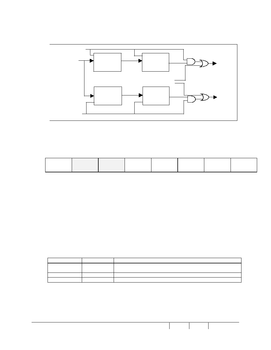
Solomon Systech
Oct 2003 P 46/144
Rev 1.4
SSD1905
7.2.9 Pulse Width Modulation (PWM) Clock and Contrast Voltage (CV) Pulse Configuration
Registers
PWM Clock
Divider
Clock Source/ 2
m
PWMCLK
m = PWM Clock Divide Select value
x = CV Pulse Divide Select value
CV Pulse
Divider
Clock Source/ 2
x
PWM Clock Force High
CV Pulse Enable
Divided
Clock
Divided
Clock
PWM Clock Enable
PWM Duty Cycle
Modulation
Duty = n / 256
CV Pulse Burst
Generation
y-pulse burst
y = Burst Length value
CV Pulse Force High
LPWMOUT
LCVOUT
Frequency =
Clock Source / (2
m
X 256)
Frequency =
Clock Source / (2
x
X 2)
n = PWM Clock Duty Cycle
Figure 7-2 : PWM Clock/CV Pulse Block Diagram
Note
For further information on PWMCLK, see Section 11.1.4 "PWMCLK".
PWM Clock / CV Pulse Control Register
REG[B0h]
Bit
7 6 5 4 3 2 1 0
PWM
Clock
Force High
0
0
PWM Clock
Enable
CV Pulse
Force High
CV Pulse
Burst
Status
CV Pulse
Burst Start
CV Pulse
Enable
Type
RW
NA
NA
RW
RW
RO
RW
RW
Reset
state
0 0 0 0 0 0 0 0
Bit 7 and Bit 4
PWM Clock Force High (bit 7) and PWM Clock Enable (bit 4)
These bits control the LPWMOUT and PWM Clock circuitry as Table 7-14 : PWM
Clock Control.
When LPWMOUT is forced low or forced high it can be used as a general purpose
output.
Note
The PWM Clock circuitry is disabled when Power Saving Mode is enabled.
Table 7-14 : PWM Clock Control
Bit 7
Bit 4
Result
0
1
PWM Clock circuitry enabled
(controlled by REG[B1h] and REG[B3h])
0
0
LPWMOUT forced low
1
x
LPWMOUT forced high
x = don't care
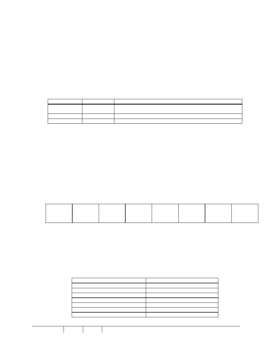
SSD1905
Rev 1.4
P 47/144 Oct 2003
Solomon Systech
Bit 3 and Bit 0
CV Pulse Force High (bit 3) and CV Pulse Enable (bit 0)
These bits control the LCVOUT pin and CV Pulse circuitry as Table 7-15 : CV Pulse
Control.
When LCVOUT is forced low or forced high it can be used as a general purpose
output.
Note
Bit 3 must be set to 0 and bit 0 must be set to 1 before initiating a new burst using the
CV Pulse Burst Start bit.
The CV Pulse circuitry is disabled when Power Saving Mode is enabled.
Table 7-15 : CV Pulse Control
Bit 3
Bit 0
Result
0
1
CV Pulse circuitry enabled
(controlled by REG[B1h] and REG[B2h])
0
0
LCVOUT forced low
1
x
LCVOUT forced high
x = don't care
Bit 2
CV Pulse Burst Status
A "1" indicates a CV pulse burst is occurring. A "0" indicates no CV pulse burst is
occurring. Software should wait for this bit to clear before starting another burst.
Bit 1
CV Pulse Burst Start
A "1" in this bit initiates a single LCVOUT pulse burst. The number of clock pulses
generated is programmable from 1 to 256. The frequency of the pulses is the divided
CV Pulse source divided by 2, with 50/50 duty cycle. This bit should be cleared to 0 by
software before initiating a new burst.
Note
This bit has effect only if the CV Pulse Enable bit is 1.
PWM Clock / CV Pulse Configuration Register
REG[B1h]
Bit
7 6 5 4 3 2 1 0
PWM
Clock
Divide
Select
Bit 3
PWM Clock
Divide
Select
Bit 2
PWM Clock
Divide
Select
Bit 1
PWM Clock
Divide
Select
Bit 0
CV Pulse
Divide
Select
Bit 2
CV Pulse
Divide
Select
Bit 1
CV Pulse
Divide
Select
Bit 0
PWMCLK
Source
Select
Type
RW
RW RW RW RW RW RW RW
Reset
state
0 0 0 0 0 0 0 0
Bits 7-4
PWM Clock Divide Select Bits [3:0]
The value of these bits represents the power of 2 by which the selected PWM clock
source is divided.
Note
This divided clock is further divided by 256 before it is output at LPWMOUT.
Table 7-16 : PWM Clock Divide Select Options
PWM Clock Divide Select Bits [3:0]
PWM Clock Divide Amount
0h 1
1h 2
2h 4
3h 8
... ...
Ch 4096
Dh-Fh 1
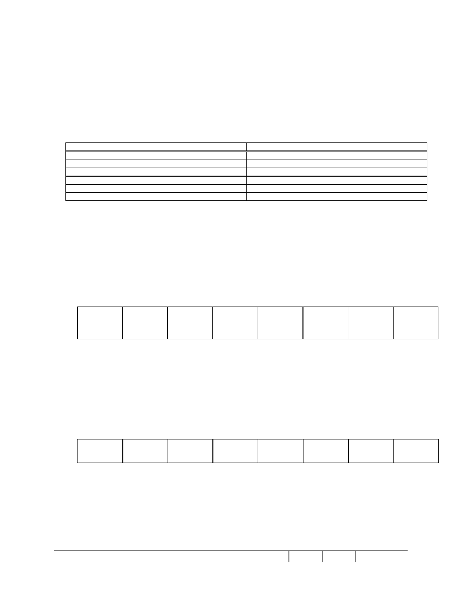
Solomon Systech
Oct 2003 P 48/144
Rev 1.4
SSD1905
Bits 3-1
CV Pulse Divide Select Bits [2:0]
The value of these bits represents the power of 2 by which the selected CV Pulse
source is divided.
Note
This divided clock is further divided by 2 before it is output at the LCVOUT.
Table 7-17 : CV Pulse Divide Select Options
CV Pulse Divide Select Bits [2:0]
CV Pulse Divide Amount
0h 1
1h 2
2h 4
3h 8
... ...
7h 128
Bit 0
PWMCLK Source Select
When this bit = 0, the clock source for PWMCLK is CLKI.
When this bit = 1, the clock source for PWMCLK is AUXCLK.
Note
For further information on the PWMCLK source select, see Section 11 "Clocks".
CV Pulse Burst Length Register
REG[B2h]
Bit
7 6 5 4 3 2 1 0
CV
Pulse
Burst
Length
Bit 7
CV Pulse
Burst
Length
Bit 6
CV Pulse
Burst
Length
Bit 5
CV Pulse
Burst
Length
Bit 4
CV Pulse
Burst
Length
Bit 3
CV Pulse
Burst
Length
Bit 2
CV Pulse
Burst
Length
Bit 1
CV Pulse
Burst
Length
Bit 0
Type
RW
RW RW RW RW RW RW RW
Reset
state
0 0 0 0 0 0 0 0
Bits 7-0
CV Pulse Burst Length Bits [7:0]
The value of this register determines the number of pulses generated in a single CV
Pulse burst:
Number of pulses in a burst = Bits [7:0] + 1
PWM Duty Cycle Register
REG[B3h]
Bit
7 6 5 4 3 2 1 0
PWM
Duty Cycle
Bit 7
PWM
Duty Cycle
Bit 6
PWM
Duty Cycle
Bit 5
PWM
Duty Cycle
Bit 4
PWM
Duty Cycle
Bit 3
PWM
Duty Cycle
Bit 2
PWM
Duty Cycle
Bit 1
PWM
Duty Cycle
Bit 0
Type
RW
RW RW RW RW RW RW RW
Reset
state
0 0 0 0 0 0 0 0
Bits 7-0
PWM Duty Cycle Bits [7:0]
This register determines the duty cycle of the PWM output.
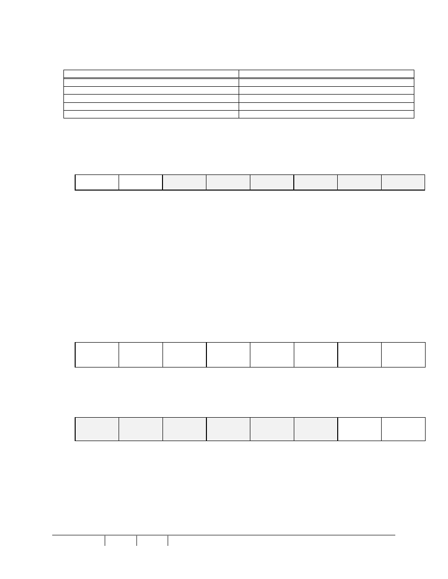
SSD1905
Rev 1.4
P 49/144 Oct 2003
Solomon Systech
Table 7-18 : PWM Duty Cycle Select Options
PWM Duty Cycle [7:0]
PWM Duty Cycle
00h Always
Low
01h
High for 1 out of 256 clock periods
02h
High for 2 out of 256 clock periods
... ...
FFh
High for 255 out of 256 clock periods.
7.2.10 Cursor Mode Registers
Cursor Feature Register
REG[C0h]
Bit
7 6 5 4 3 2 1 0
Cursor1
Enable
Cursor2
Enable
0
0
0
0
0
0
Type
RW
RW
NA
NA
NA
NA
NA
NA
Reset
state
0 0 0 0 0 0 0 0
Bit 7
Cursor1 Enable
When this bit = 0 Cursor1 is disabled.
When this bit = 1 Cursor1 is enabled.
Bit 6
Cursor2 Enable
When this bit = 0, Cursor2 is disabled.
When this bit = 1, Cursor2 is enabled.
Note
This register is effective for 4/8/16 bpp (REG[70h] Bits 2:0 = 010/011/100)
For Hardware Cursors operation, see Section 20 "Hardware Cursor Mode".
Cursor1 Blink Total Register 0
REG[C4h]
Bit
7 6 5 4 3 2 1 0
Cursor1
Blink Total
Bit 7
Cursor1
Blink Total
Bit 6
Cursor1
Blink Total
Bit 5
Cursor1
Blink Total
Bit 4
Cursor1
Blink Total
Bit 3
Cursor1
Blink Total
Bit 2
Cursor1
Blink Total
Bit 1
Cursor1
Blink Total
Bit 0
Type
RW
RW
RW
RW
RW
RW
RW
RW
Reset
state
0 0 0 0 0 0 0 0
Cursor1 Blink Total Register 1
REG[C5h]
Bit
7 6 5 4 3 2 1 0
0
0
0
0
0
0
Cursor1
Blink Total
Bit 9
Cursor1
Blink Total
Bit 8
Type
NA
NA
NA
NA
NA
NA
RW
RW
Reset
state
0 0 0 0 0 0 0 0
REG[C5h] bits 1-0,
REG[C4h] bits 7-0
Cursor1 Blink Total Bits [9:0]
This is the total blinking period per frame for cursor1. This register must be set to a
non-zero value in order to make the cursor visible.
Note
These bits will not effective until the Cursor1 Enable bit is set to 1 (REG[C0h] bit 7=1).

Solomon Systech
Oct 2003 P 50/144
Rev 1.4
SSD1905
Cursor1 Blink On Register 0
REG[C8h]
Bit
7 6 5 4 3 2 1 0
Cursor1
Blink On Bit
7
Cursor1
Blink On Bit
6
Cursor1
Blink On Bit
5
Cursor1
Blink On Bit
4
Cursor1
Blink On Bit
3
Cursor1
Blink On Bit
2
Cursor1
Blink On Bit
1
Cursor1
Blink On Bit
0
Type
RW
RW
RW
RW
RW
RW
RW
RW
Reset
state
0 0 0 0 0 0 0 0
Cursor1 Blink On Register 1
REG[C9h]
Bit
7 6 5 4 3 2 1 0
0
0
0
0
0
0
Cursor1
Blink On Bit
9
Cursor1
Blink On Bit
8
Type
NA NA NA NA NA NA RW
RW
Reset
state
0 0 0 0 0 0 0 0
REG[C9h] bits 1-0,
REG[C8h] bits 7-0
Cursor1 Blink On Bits [9:0]
This is the blink on frame period for Cursor1. This register must be set to a non-zero
value in order to make the cursor1 visible. Also, cursor1 will start to blink if the
following conditions are fulfilled :
Cursor1 Blink Total Bits [9:0] > Cursor1 Blink On Bits [9:0] > 0
Note:
To enable cursor1 without blinking, user must program cursor1 blink on register with a
non-zero value, and this value must be greater than or equal to Cursor1 Blink Total
Register.
These bits will not effective until the Cursor1 Enable bit is set to 1 (REG[C0h] bit 7=1).
Cursor1 Memory Start Register 0
REG[CCh]
Bit
7 6 5 4 3 2 1 0
Cursor1
Memory
Start Bit 7
Cursor1
Memory
Start Bit 6
Cursor1
Memory
Start Bit 5
Cursor1
Memory
Start Bit 4
Cursor1
Memory
Start Bit 3
Cursor1
Memory
Start Bit 2
Cursor1
Memory
Start Bit 1
Cursor1
Memory
Start Bit 0
Type
RW
RW
RW
RW
RW
RW
RW
RW
Reset
state
0 0 0 0 0 0 0 0
Cursor1 Memory Start Register 1
REG[CDh]
Bit
7 6 5 4 3 2 1 0
Cursor1
Memory
Start Bit 15
Cursor1
Memory
Start Bit 14
Cursor1
Memory
Start Bit 13
Cursor1
Memory
Start Bit 12
Cursor1
Memory
Start Bit 11
Cursor1
Memory
Start Bit 10
Cursor1
Memory
Start Bit 9
Cursor1
Memory
Start Bit 8
Type
RW
RW
RW
RW
RW
RW
RW
RW
Reset
state
0 0 0 0 0 0 0 0
Cursor1 Memory Start Register 2
REG[CEh]
Bit
7 6 5 4 3 2 1 0
0
0
0
0
0
0
0
Cursor1
Memory
Start Bit 16
Type
NA
NA
NA
NA
NA
NA
NA
RW
Reset
state
0 0 0 0 0 0 0 0

SSD1905
Rev 1.4
P 51/144 Oct 2003
Solomon Systech
REG[CEh] bit 0,
REG[CDh] bits 7-0
REG[CCh] bits 7-0
Cursor1 Memory Start Bits [16:0]
This is the start location of memory buffer for Cursor1 image.
Note
These bits will not effective until the Cursor1 Enable bit is set to 1 (REG[C0h] bit 7=1).
Cursor1 Position X Register 0
REG[D0h]
Bit
7 6 5 4 3 2 1 0
Cursor1
Position X
Bit 7
Cursor1
Position X
Bit 6
Cursor1
Position X
Bit 5
Cursor1
Position X
Bit 4
Cursor1
Position X
Bit 3
Cursor1
Position X
Bit 2
Cursor1
Position X
Bit 1
Cursor1
Position X
Bit 0
Type
RW
RW
RW
RW
RW
RW
RW
RW
Reset
state
0 0 0 0 0 0 0 0
Cursor1 Position X Register 1
REG[D1h]
Bit
7 6 5 4 3 2 1 0
0
0
0
0
0
0
Cursor1
Position X
Bit 9
Cursor1
Position X
Bit 8
Type
NA
NA
NA
NA
NA
NA
RW
RW
Reset
state
0 0 0 0 0 0 0 0
REG[D1h] bits 1-0,
REG[D0h] bits 7-0
Cursor1 Position X Bits [9:0]
This is starting position X of Cursor1 image. The definition of this register is same as
Floating Window Start Position X Register.
Note
These bits will not effective until the Cursor1 Enable bit is set to 1 (REG[C0h] bit 7=1).
Cursor1 Position Y Register 0
REG[D4h]
Bit
7 6 5 4 3 2 1 0
Cursor1
Position Y
Bit 7
Cursor1
Position Y
Bit 6
Cursor1
Position Y
Bit 5
Cursor1
Position Y
Bit 4
Cursor1
Position Y
Bit 3
Cursor1
Position Y
Bit 2
Cursor1
Position Y
Bit 1
Cursor1
Position Y
Bit 0
Type
RW
RW
RW
RW
RW
RW
RW
RW
Reset
state
0 0 0 0 0 0 0 0
Cursor1 Position Y Register 1
REG[D5h]
Bit
7 6 5 4 3 2 1 0
0
0
0
0
0
0
Cursor1
Position Y
Bit 9
Cursor1
Position Y
Bit 8
Type
NA
NA
NA
NA
NA
NA
RW
RW
Reset
state
0 0 0 0 0 0 0 0
REG[D5h] bits 1-0,
REG[D4h] bits 7-0
Cursor1 Position Y Bits [9:0]
This is starting position Y of Cursor1 image. The definition of this register is same as
Floating Window Y Start Position Register.
Note
These bits will not effective until the Cursor1 Enable bit is set to 1 (REG[C0h] bit 7=1).
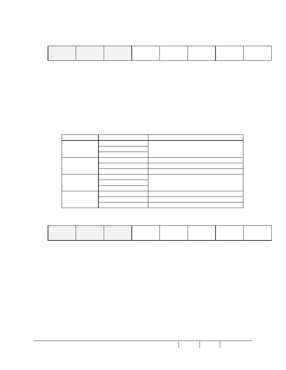
Solomon Systech
Oct 2003 P 52/144
Rev 1.4
SSD1905
Cursor1 Horizontal Size Register
REG[D8h]
Bit
7 6 5 4 3 2 1 0
0
0
0
Cursor1
Horizontal
Size Bit 4
Cursor1
Horizontal
Size Bit 3
Cursor1
Horizontal
Size Bit 2
Cursor1
Horizontal
Size Bit 1
Cursor1
Horizontal
Size Bit 0
Type
NA
NA
NA
RW
RW
RW
RW
RW
Reset
state
0 0 0 0 0 0 0 0
Bits 4-0
Cursor1 Horizontal Size Bits [4:0]
These bits specify the horizontal size of Cursor1.
Note :
The definition of this register various under different panel orientation and color depth
settings.
These bits will not effective until the Cursor1 Enable bit is set to 1 (REG[C0h] bit 7=1).
Table 7-19 : X Increment Mode for Various Color Depths
Orientation
Color Depths (bpp)
Increment (x)
4
8
0�
16
16 pixel increment
e.g. 00000b = 16 pixel; 00001b = 32 pixel
4
2 line increment
8
4 line increment
90�
16
8 line increment
4
8
180�
16
16 pixel increment
4
2 line increment
8
4 line increment
270�
16
8 line increment
Cursor1 Vertical Size Register
REG[DCh]
Bit
7 6 5 4 3 2 1 0
0
0
0
Cursor1
Vertical
Size Bit 4
Cursor1
Vertical
Size Bit 3
Cursor1
Vertical
Size Bit 2
Cursor1
Vertical
Size Bit 1
Cursor1
Vertical
Size Bit 0
Type
NA
NA
NA
RW
RW
RW
RW
RW
Reset
state
0 0 0 0 0 0 0 0
Bits 4-0
Cursor1 Vertical Size Bits [4:0]
These bits specify the vertical size of Cursor1.
Note
The definition of this register various under different panel orientation and color depth
settings.
These bits will not effective until the Cursor1 Enable bit is set to 1 (REG[C0h] bit 7=1).
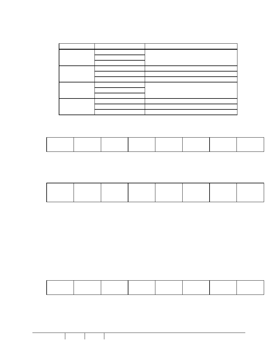
SSD1905
Rev 1.4
P 53/144 Oct 2003
Solomon Systech
Table 7-20 : Y Increment Mode for Various Color Depths
Orientation
Color Depths (bpp)
Increment (y)
4
8
0�
16
1 line increment
e.g. 00000b = 1 line; 00001b = 2 lines
4
8 pixel increment
8
4 pixel increment
90�
16
2 pixel increment
4
8
180�
16
1 line increment
4
8 pixel increment
8
4 pixel increment
270�
16
2 pixel increment
Cursor1 Color Index1 Register 0
REG[E0h]
Bit
7 6 5 4 3 2 1 0
Cursor1
Color
Index1 Bit 7
Cursor1
Color
Index1 Bit 6
Cursor1
Color
Index1 Bit 5
Cursor1
Color
Index1 Bit 4
Cursor1
Color
Index1 Bit 3
Cursor1
Color
Index1 Bit 2
Cursor1
Color
Index1 Bit 1
Cursor1
Color
Index1 Bit 0
Type
RW
RW
RW
RW
RW
RW
RW
RW
Reset
state
0 0 0 0 0 0 0 0
Cursor1 Color Index1 Register 1
REG[E1h]
Bit
7 6 5 4 3 2 1 0
Cursor1
Color
Index1 Bit
15
Cursor1
Color
Index1 Bit
14
Cursor1
Color
Index1 Bit
13
Cursor1
Color
Index1 Bit
12
Cursor1
Color
Index1 Bit
11
Cursor1
Color
Index1 Bit
10
Cursor1
Color
Index1 Bit
9
Cursor1
Color
Index1 Bit
8
Type
RW
RW
RW
RW
RW
RW
RW
RW
Reset
state
0 0 0 0 0 0 0 0
REG[E1h] bits 7-0,
REG[E0h] bits 7-0
Cursor1 Color Index1 Bits [15:0]
Each cursor pixel is represented by 2 bits. This register stores the color index for pixel
value 01 of Cursor1, refer to Table 20-1.
Note
These bits will not effective until the Cursor1 Enable bit is set to 1 (REG[C0h] bit 7=1).
For Hardware Cursors operation, see Section 20 "Hardware Cursor Mode".
Cursor1 Color Index2 Register 0
REG[E4h]
Bit
7 6 5 4 3 2 1 0
Cursor1
Color
Index2 Bit 7
Cursor1
Color
Index2 Bit 6
Cursor1
Color
Index2 Bit 5
Cursor1
Color
Index2 Bit 4
Cursor1
Color
Index2 Bit 3
Cursor1
Color
Index2 Bit 2
Cursor1
Color
Index2 Bit 1
Cursor1
Color
Index2 Bit 0
Type
RW
RW
RW
RW
RW
RW
RW
RW
Reset
state
0 0 0 0 0 0 0 0

Solomon Systech
Oct 2003 P 54/144
Rev 1.4
SSD1905
Cursor1 Color Index2 Register 1
REG[E5h]
Bit
7 6 5 4 3 2 1 0
Cursor1
Color
Index2 Bit
15
Cursor1
Color
Index2 Bit
14
Cursor1
Color
Index2 Bit
13
Cursor1
Color
Index2 Bit
12
Cursor1
Color
Index2 Bit
11
Cursor1
Color
Index2 Bit
10
Cursor1
Color
Index2 Bit
9
Cursor1
Color
Index2 Bit
8
Type
RW
RW
RW
RW
RW
RW
RW
RW
Reset
state
0 0 0 0 0 0 0 0
REG[E5h] bits 7-0,
REG[E4h] bits 7-0
Cursor1 Color Index2 Bits [15:0]
Each cursor pixel is represented by 2 bits. This register stores the color index for pixel
value 10 of Cursor1, refer to Table 20-1.
Note
These bits will not effective until the Cursor1 Enable bit is set to 1 (REG[C0h] bit 7=1).
For Hardware Cursors operation, see Section 20 "Hardware Cursor Mode".
Cursor1 Color Index3 Register 0
REG[E8h]
Bit
7 6 5 4 3 2 1 0
Cursor1
Color
Index3 Bit 7
Cursor1
Color
Index3 Bit 6
Cursor1
Color
Index3 Bit 5
Cursor1
Color
Index3 Bit 4
Cursor1
Color
Index3 Bit 3
Cursor1
Color
Index3 Bit 2
Cursor1
Color
Index3 Bit 1
Cursor1
Color
Index3 Bit 0
Type
RW
RW
RW
RW
RW
RW
RW
RW
Reset
state
0 0 0 0 0 0 0 0
Cursor1 Color Index3 Register 1
REG[E9h]
Bit
7 6 5 4 3 2 1 0
Cursor1
Color
Index3 Bit
15
Cursor1
Color
Index3 Bit
14
Cursor1
Color
Index3 Bit
13
Cursor1
Color
Index3 Bit
12
Cursor1
Color
Index3 Bit
11
Cursor1
Color
Index3 Bit
10
Cursor1
Color
Index3 Bit
9
Cursor1
Color
Index3 Bit
8
Type
RW
RW
RW
RW
RW
RW
RW
RW
Reset
state
0 0 0 0 0 0 0 0
REG[E9h] bits 7-0,
REG[E8h] bits 7-0
Cursor1 Color Index3 Bits [15:0]
Each cursor pixel is represented by 2 bits. This register stores the color index for pixel
value 11 of Cursor1, refer to Table 20-1.
Note
These bits will not effective until the Cursor1 Enable bit is set to 1 (REG[C0h] bit 7=1).
For Hardware Cursors operation, see Section 20 "Hardware Cursor Mode".
Cursor2 Blink Total Register 0
REG[ECh]
Bit
7 6 5 4 3 2 1 0
Cursor2
Blink Total
Bit 7
Cursor2
Blink Total
Bit 6
Cursor2
Blink Total
Bit 5
Cursor2
Blink Total
Bit 4
Cursor2
Blink Total
Bit 3
Cursor2
Blink Total
Bit 2
Cursor2
Blink Total
Bit 1
Cursor2
Blink Total
Bit 0
Type
RW
RW
RW
RW
RW
RW
RW
RW
Reset
state
0 0 0 0 0 0 0 0

SSD1905
Rev 1.4
P 55/144 Oct 2003
Solomon Systech
Cursor2 Blink Total Register 1
REG[EDh]
Bit
7 6 5 4 3 2 1 0
0
0
0
0
0
0
Cursor2
Blink Total
Bit 9
Cursor2
Blink Total
Bit 8
Type
NA
NA
NA
NA
NA
NA
RW
RW
Reset
state
0 0 0 0 0 0 0 0
REG[EDh] bits 1-0,
REG[ECh] bits 7-0
Cursor2 Blink Total Bits [9:0]
This is the total blinking period per frame for Cursor2. This register must be set to a
non-zero value in order to make the cursor visible.
Note
These bits will not effective until the Cursor2 Enable bit is set to 1 (REG[C0h] bit 6=1).
Cursor2 Blink On Register 0
REG[F0h]
Bit
7 6 5 4 3 2 1 0
Cursor2
Blink On Bit
7
Cursor2
Blink On Bit
6
Cursor2
Blink On Bit
5
Cursor2
Blink On Bit
4
Cursor2
Blink On Bit
3
Cursor2
Blink On Bit
2
Cursor2
Blink On Bit
1
Cursor2
Blink On Bit
0
Type
RW
RW
RW
RW
RW
RW
RW
RW
Reset
state
0 0 0 0 0 0 0 0
Cursor2 Blink On Register 1
REG[F1h]
Bit
7 6 5 4 3 2 1 0
0
0
0
0
0
0
Cursor2
Blink On Bit
9
Cursor2
Blink On Bit
8
Type
NA
NA
NA
NA
NA
NA
RW
RW
Reset
state
0 0 0 0 0 0 0 0
REG[F1h] bits 1-0,
REG[F0h] bits 7-0
Cursor2 Blink On Bits [9:0]
This is the blink on frame period for Cursor2. This register must be set to a non-zero
value in order to make the Cursor2 visible. Also, Cursor2 will start to blink if the
following conditions are fulfilled:
Cursor2 Blink Total Bits [9:0] > Cursor2 Blink On Bits [9:0] > 0
Note
To enable Cursor2 without blinking, user must program Cursor2 Blink On Register with
a non-zero value, and this value must be greater than or equal to Cursor2 Blink Total
Register.
These bits will not effective until the Cursor2 Enable bit is set to 1 (REG[C0h] bit 6=1).
Cursor2 Memory Start Register 0
REG[F4h]
Bit
7 6 5 4 3 2 1 0
Cursor2
Memory
Start Bit 7
Cursor2
Memory
Start Bit 6
Cursor2
Memory
Start Bit 5
Cursor2
Memory
Start Bit 4
Cursor2
Memory
Start Bit 3
Cursor2
Memory
Start Bit 2
Cursor2
Memory
Start Bit 1
Cursor2
Memory
Start Bit 0
Type
RW
RW
RW
RW
RW
RW
RW
RW
Reset
state
0 0 0 0 0 0 0 0

Solomon Systech
Oct 2003 P 56/144
Rev 1.4
SSD1905
Cursor2 Memory Start Register 1
REG[F5h]
Bit
7 6 5 4 3 2 1 0
Cursor2
Memory
Start Bit 15
Cursor2
Memory
Start Bit 14
Cursor2
Memory
Start Bit 13
Cursor2
Memory
Start Bit 12
Cursor2
Memory
Start Bit 11
Cursor2
Memory
Start Bit 10
Cursor2
Memory
Start Bit 9
Cursor2
Memory
Start Bit 8
Type
RW
RW
RW
RW
RW
RW
RW
RW
Reset
state
0 0 0 0 0 0 0 0
Cursor2 Memory Start Register 2
REG[F6h]
Bit
7 6 5 4 3 2 1 0
0
0
0
0
0
0
0
Cursor2
Memory
Start Bit 16
Type
NA
NA
NA
NA
NA
NA
NA
RW
Reset
state
0
0
0
0
0
0
0
0
REG[F6h] bit 0,
REG[F5h] bits 7-0,
REG[F4h] bits 7-0
Cursor2 Memory Start Bits [16:0]
This is the start location of memory buffer for Cursor2 image.
Note
These bits will not effective until the Cursor2 Enable bit is set to 1 (REG[C0h] bit 6=1).
Cursor2 Position X Register 0
REG[F8h]
Bit
7 6 5 4 3 2 1 0
Cursor2
Position X
Bit 7
Cursor2
Position X
Bit 6
Cursor2
Position X
Bit 5
Cursor2
Position X
Bit 4
Cursor2
Position X
Bit 3
Cursor2
Position X
Bit 2
Cursor2
Position X
Bit 1
Cursor2
Position X
Bit 0
Type
RW
RW
RW
RW
RW
RW
RW
RW
Reset
state
0 0 0 0 0 0 0 0
Cursor2 Position X Register 1
REG[F9h]
Bit
7 6 5 4 3 2 1 0
0
0
0
0
0
0
Cursor2
Position X
Bit 9
Cursor2
Position X
Bit 8
Type
NA
NA
NA
NA
NA
NA
RW
RW
Reset
state
0
0
0
0
0
0
0 0
REG[F9h] bits 1-0,
REG[F8h] bits 7-0
Cursor2 Position X Bits [9:0]
This is starting position X of Cursor2 image. The definition of this register is same as
Floating Window Start Position X Register.
Note
These bits will not effective until the Cursor2 Enable bit is set to 1 (REG[C0h] bit 6=1).
Cursor2 Position Y Register 0
REG[FCh]
Bit
7 6 5 4 3 2 1 0
Cursor2
Position Y
Bit 7
Cursor2
Position Y
Bit 6
Cursor2
Position Y
Bit 5
Cursor2
Position Y
Bit 4
Cursor2
Position Y
Bit 3
Cursor2
Position Y
Bit 2
Cursor2
Position Y
Bit 1
Cursor2
Position Y
Bit 0
Type
RW
RW
RW
RW
RW
RW
RW
RW
Reset
state
0 0 0 0 0 0 0 0

SSD1905
Rev 1.4
P 57/144 Oct 2003
Solomon Systech
Cursor2 Position Y Register 1
REG[FDh]
Bit
7 6 5 4 3 2 1 0
0
0
0
0
0
0
Cursor2
Position Y
Bit 9
Cursor2
Position Y
Bit 8
Type
NA
NA
NA
NA
NA
NA
RW
RW
Reset
state
0 0 0 0 0 0 0 0
REG[FDh] bits 1-0,
REG[FCh] bits 7-0
Cursor2 Position Y Bits [9:0]
This is starting position Y of Cursor2 image. The definition of this register is same as
Floating Window Y Start Position Register.
Note
These bits will not effective until the Cursor2 Enable bit is set to 1 (REG[C0h] bit 6=1).
Cursor2 Horizontal Size Register
REG[100h]
Bit
7 6 5 4 3 2 1 0
0
0
0
Cursor2
Horizontal
Size Bit 4
Cursor2
Horizontal
Size Bit 3
Cursor2
Horizontal
Size Bit 2
Cursor2
Horizontal
Size Bit 1
Cursor2
Horizontal
Size Bit 0
Type
NA
NA
NA
RW
RW
RW
RW
RW
Reset
state
0 0 0 0 0 0 0 0
Bits 4-0
Cursor2 Horizontal Size Bits [4:0]
These bits specify the horizontal size of Cursor2.
Note :
The definition of this register various under different panel orientation and color depth
settings. Refer to Table 7-19 : X Increment Mode for Various Color Depths.
These bits will not effective until the Cursor2 Enable bit is set to 1 (REG[C0h] bit 6=1).
Cursor2 Vertical Size Register
REG[104h]
Bit
7 6 5 4 3 2 1 0
0
0
0
Cursor2
Vertical
Size Bit 4
Cursor2
Vertical
Size Bit 3
Cursor2
Vertical
Size Bit 2
Cursor2
Vertical
Size Bit 1
Cursor2
Vertical
Size Bit 0
Type
NA
NA
NA
RW
RW
RW
RW
RW
Reset
state
0 0 0 0 0 0 0 0
Bits 4-0
Cursor2 Vertical Size Bits [4:0]
These bits specify the vertical size of Cursor2.
Note :
The definition of this register various under different panel orientation and color depth
settings. Refer to Table 7-20 : Y Increment Mode for Various Color Depths.
These bits will not effective until the Cursor2 Enable bit is set to 1 (REG[C0h] bit 6=1).

Solomon Systech
Oct 2003 P 58/144
Rev 1.4
SSD1905
Cursor2 Color Index1 Register 0
REG[108h]
Bit
7 6 5 4 3 2 1 0
Cursor2
Color
Index1 Bit 7
Cursor2
Color
Index1 Bit 6
Cursor2
Color
Index1 Bit 5
Cursor2
Color
Index1 Bit 4
Cursor2
Color
Index1 Bit 3
Cursor2
Color
Index1 Bit 2
Cursor2
Color
Index1 Bit 1
Cursor2
Color
Index1 Bit 0
Type
RW
RW
RW
RW
RW
RW
RW
RW
Reset
state
0 0 0 0 0 0 0 0
Cursor2 Color Index1 Register 1
REG[109h]
Bit
7 6 5 4 3 2 1 0
Cursor2
Color
Index1 Bit
15
Cursor2
Color
Index1 Bit
14
Cursor2
Color
Index1 Bit
13
Cursor2
Color
Index1 Bit
12
Cursor2
Color
Index1 Bit
11
Cursor2
Color
Index1 Bit
10
Cursor2
Color
Index1 Bit 9
Cursor2
Color
Index1 Bit 8
Type
RW
RW
RW
RW
RW
RW
RW
RW
Reset
state
0 0 0 0 0 0 0 0
REG[109h] bits 7-0
REG[108h] bits 7-0
Cursor2 Color Index1 Bits [15:0]
Each cursor pixel is represented by 2 bits. This register stores the color index for pixel
value 01 of Cursor2, refer to Table 20-1.
Note
These bits will not effective until the Cursor2 Enable bit is set to 1 (REG[C0h] bit 6=1).
For Hardware Cursors operation, see Section 20 "Hardware Cursor Mode".
Cursor2 Color Index2 Register 0
REG[10Ch]
Bit
7 6 5 4 3 2 1 0
Cursor2
Color
Index2 Bit 7
Cursor2
Color
Index2 Bit 6
Cursor2
Color
Index2 Bit 5
Cursor2
Color
Index2 Bit 4
Cursor2
Color
Index2 Bit 3
Cursor2
Color
Index2 Bit 2
Cursor2
Color
Index2 Bit 1
Cursor2
Color
Index2 Bit 0
Type
RW
RW
RW
RW
RW
RW
RW
RW
Reset
state
0 0 0 0 0 0 0 0
Cursor2 Color Index2 Register 1
REG[10Dh]
Bit
7 6 5 4 3 2 1 0
Cursor2
Color
Index2 Bit
15
Cursor2
Color
Index2 Bit
14
Cursor2
Color
Index2 Bit
13
Cursor2
Color
Index2 Bit
12
Cursor2
Color
Index2 Bit
11
Cursor2
Color
Index2 Bit
10
Cursor2
Color
Index2 Bit 9
Cursor2
Color
Index2 Bit 8
Type
RW
RW
RW
RW
RW
RW
RW
RW
Reset
state
0 0 0 0 0 0 0 0
REG[10Dh] bits 7-0
REG[10Ch] bits 7-0
Cursor2 Color Index2 Bits [15:0]
Each cursor pixel is represented by 2 bits. This register stores the color index for pixel
value 10 of Cursor2, refer to Table 20-1.
Note
These bits will not effective until the Cursor2 Enable bit is set to 1 (REG[C0h] bit 6=1).
For Hardware Cursors operation, see Section 20 "Hardware Cursor Mode".

SSD1905
Rev 1.4
P 59/144 Oct 2003
Solomon Systech
Cursor2 Color Index3 Register 0
REG[110h]
Bit
7 6 5 4 3 2 1 0
Cursor2
Color
Index3 Bit 7
Cursor2
Color
Index3 Bit 6
Cursor2
Color
Index3 Bit 5
Cursor2
Color
Index3 Bit 4
Cursor2
Color
Index3 Bit 3
Cursor2
Color
Index3 Bit 2
Cursor2
Color
Index3 Bit 1
Cursor2
Color
Index3 Bit 0
Type
RW
RW
RW
RW
RW
RW
RW
RW
Reset
state
0 0 0 0 0 0 0 0
Cursor2 Color Index3 Register 1
REG[111h]
Bit
7 6 5 4 3 2 1 0
Cursor2
Color
Index3 Bit
15
Cursor2
Color
Index3 Bit
14
Cursor2
Color
Index3 Bit
13
Cursor2
Color
Index3 Bit
12
Cursor2
Color
Index3 Bit
11
Cursor2
Color
Index3 Bit
10
Cursor2
Color
Index3 Bit 9
Cursor2
Color
Index3 Bit 8
Type
RW
RW
RW
RW
RW
RW
RW
RW
Reset
state
0 0 0 0 0 0 0 0
REG[111h] bits 7-0
REG[110h] bits 7-0
Cursor2 Color Index3 Bits [15:0]
Each cursor pixel is represented by 2 bits. This register stores the color index for pixel
value 11 of Cursor2, refer to Table 20-1.
Note
These bits will not effective until the Cursor2 Enable bit is set to 1 (REG[C0h] bit 6=1).
For Hardware Cursors operation, see Section 20 "Hardware Cursor Mode".
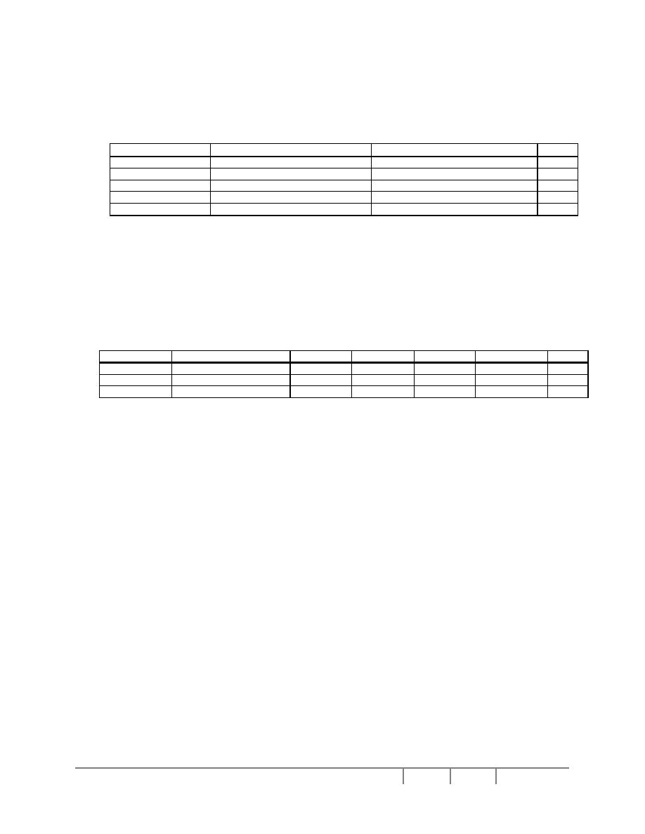
Solomon Systech
Oct 2003 P 60/144
Rev 1.4
SSD1905
8 MAXIMUM
RATINGS
Table 8-1 : Absolute Maximum Ratings
Symbol Parameter
Rating
Units
IOV
DD
Supply
Voltage
V
SS
- 0.3 to 4.0
V
V
IN
Input
Voltage
V
SS
- 0.3 to 5.0
V
V
OUT
Output
Voltage
V
SS
- 0.3 to IOV
DD
+ 0.5
V
T
STG
Storage Temperature
-65 to 150
�C
T
SOL
Solder Temperature/Time
260 for 10 sec. max at lead
�C
Maximum Ratings are those values beyond which damage to the device may occur. Functional operation should be
restricted to the limits in the Electrical Characteristics tables or Pin Description section.
This device contains circuitry to protect the inputs against damage due to high static voltages or electric fields;
however, it is advised that normal precautions to be taken to avoid application of any voltage higher than maximum
rated voltages to this high impedance circuit. For proper operation it is recommended that V
IN
and V
OUT
be
constrained to the range V
SS
(V
IN
or V
OUT
)
IOV
DD
. Reliability of operation is enhanced if unused input are
connected to an appropriate logic voltage level (e.g., either V
SS
or IOV
DD
). This device is not radiation protected.
Table 8-2 : Recommended Operating Conditions
Symbol Parameter
Condition
Min Typ Max
Units
IOV
DD
Supply
Voltage V
SS
= 0V
3.0
3.3
3.6
V
V
IN
Input
Voltage V
SS
IOV
DD
V
T
OPR
Operating
Temperature
-30 25 85 �C
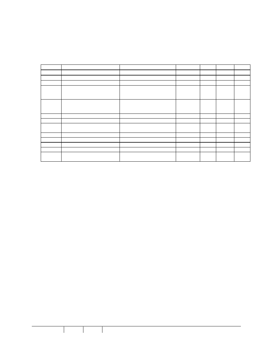
SSD1905
Rev 1.4
P 61/144 Oct 2003
Solomon Systech
9 DC
CHARACTERISTICS
Table 9-1 : Electrical Characteristics for IOV
DD
= 3.3V typical
Symbol Parameter
Condition
Min
Typ Max Units
I
DDS
Quiescent Current
Quiescent Conditions
120
�A
I
IZ
Input Leakage Current
-1
1
�A
I
OZ
Output Leakage Current
-1
1
�A
V
OH
High Level Output Voltage
IOV
DD
= min
I
OH
= -8mA (Type 2)
-12mA (Type 3)
IOV
DD
-0.4
V
V
OL
Low Level Output Voltage
IOV
DD
= min
I
OL
= 8mA (Type2)
12mA (Type 3)
0.4
V
V
IH
High Level Input Voltage
LVTTL Level, IOV
DD
= max
IOV
DD
-0.8
V
V
IL
Low Level Input Voltage
LVTTL Level, IOV
DD
= min
0.8
V
V
T+
High Level Input Voltage
LVTTL Schmitt
1.1
V
V
T-
Low Level Input Voltage
LVTTL Schmitt
0.94
V
V
H1
Hysteresis Voltage
LVTTL Schmitt
0.15
V
C
I
Input Pin Capacitance
10
pF
C
O
Output Pin Capacitance
10
pF
C
IO
Bi-Directional
Pin
Capacitance
10
pF
10 AC CHARACTERISTICS
Conditions:
IOV
DD
= 3.3V � 10%
T
A
=-30
�C to 85�C
T
rise
and T
fall
for all inputs must be < 5 ns (10% ~ 90%)
C
L
= 50pF (Bus/CPU Interface)
C
L
= 0pF (LCD Panel Interface)
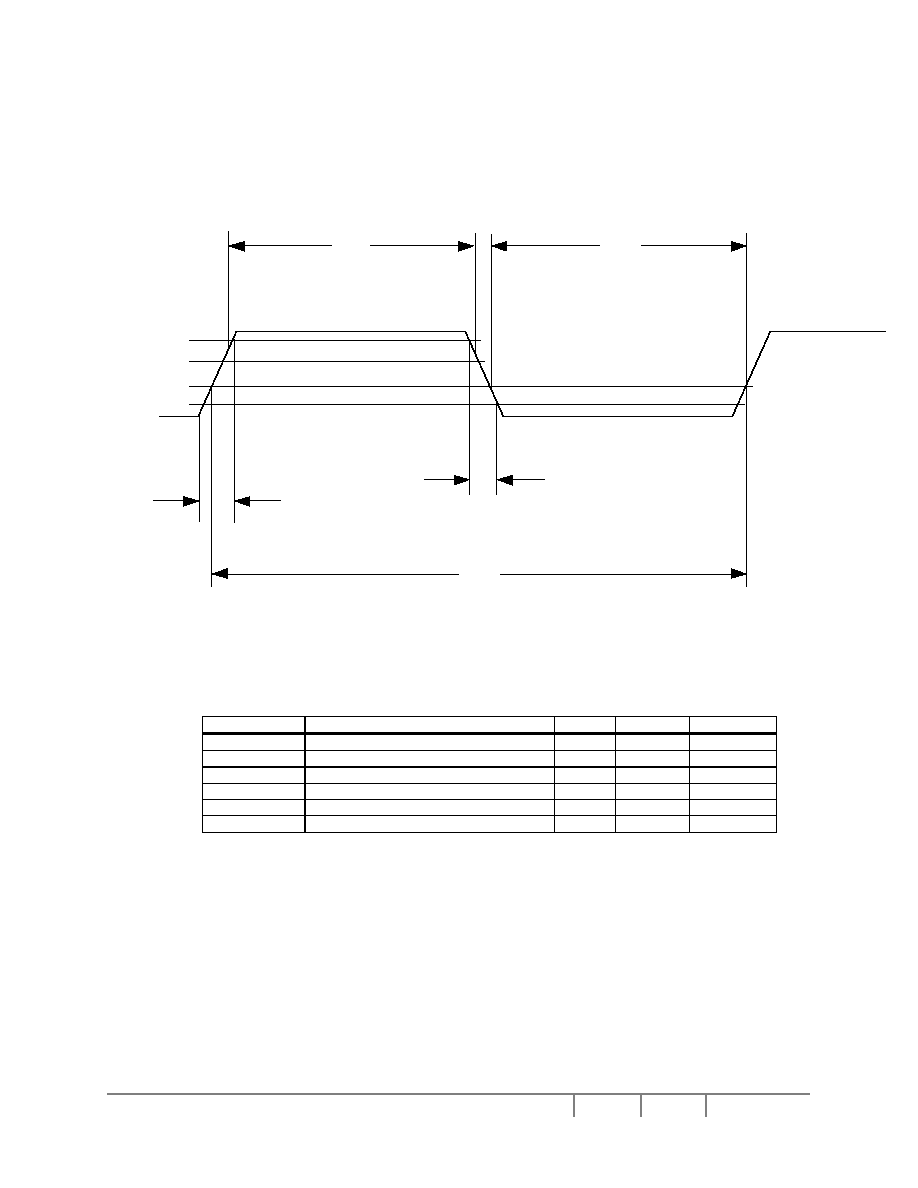
Solomon Systech
Oct 2003 P 62/144
Rev 1.4
SSD1905
10.1 Clock Timing
10.1.1 Input Clocks
90%
VIH
VIL
10%
T
OSC
t
PWL
t
PWH
t
f
t
r
Clock Input Waveform
Figure 10-1 : Clock Input Requirements
Table 10-1 : Clock Input Requirements for CLKI
Symbol
Parameter
Min
Max
Units
f
OSC
Input Clock Frequency (CLKI)
66 MHz
T
OSC
Input Clock period (CLKI)
1/f
OSC
ns
t
PWH
Input Clock Pulse Width High (CLKI)
5
ns
t
PWL
Input Clock Pulse Width Low (CLKI)
5
ns
t
f
Input Clock Fall Time (10% - 90%)
5
ns
t
r
Input Clock Rise Time (10% - 90%)
5
ns
Note
Maximum internal requirements for clocks derived from CLKI must be considered when determining the frequency
of CLKI. See Section 10.1.2 "Internal Clocks" for internal clock requirements.
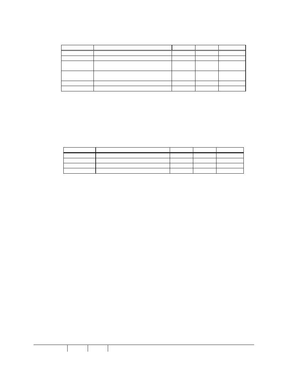
SSD1905
Rev 1.4
P 63/144 Oct 2003
Solomon Systech
Table 10-2 : Clock Input Requirements for AUXCLK
Symbol
Parameter
Min
Max
Units
f
OSC
Input Clock Frequency (AUXCLK)
66
MHz
T
OSC
Input Clock period (AUXCLK)
1/f
OSC
ns
t
PWH
Input Clock Pulse Width High
(AUXCLK)
5 ns
t
PWL
Input Clock Pulse Width Low
(AUXCLK)
5 ns
t
f
Input Clock Fall Time (10% - 90%)
5
ns
t
r
Input Clock Rise Time (10% - 90%)
5
ns
Note :
Maximum internal requirements for clocks derived from AUXCLK must be considered when determining the
frequency of AUXCLK. See Section 10.1.2 "Internal Clocks" for internal clock requirements.
10.1.2 Internal Clocks
Table 10-3 : Internal Clock Requirements
Symbol
Parameter
Min
Max
Units
f
BCLK
Bus Clock frequency
66
MHz
f
MCLK
Memory Clock frequency
55
MHz
f
PCLK
Pixel Clock frequency
55
MHz
f
PWMCLK
PWM Clock frequency
66
MHz
Note :
For further information on internal clocks, refer to Section 11 "Clocks".
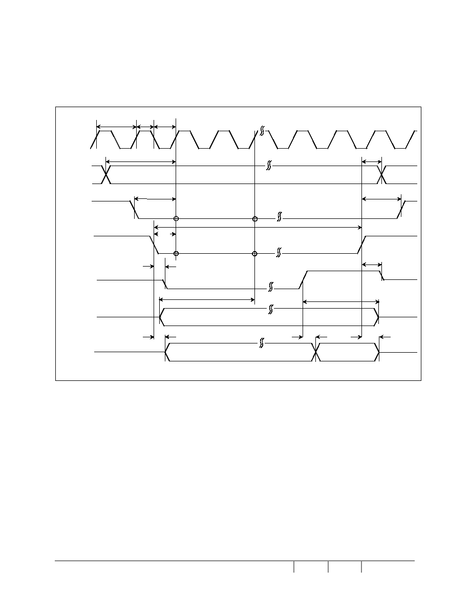
Solomon Systech
Oct 2003 P 64/144
Rev 1.4
SSD1905
10.2 CPU Interface Timing
The following section are CPU interface AC Timing based on IOV
DD
= 3.3V.
10.2.1 Generic #1 Interface Timing
t
13
t
7
t
9
A[16:1],
M/R#,
t
10
CLK
WAIT#
RD0#, RD1#
WE0#, WE1#
CS#
D[15:0]
(read)
D[15:0]
(write)
T
CLK
t
2
t
1
t
3
t
4
t
6
t
5
t
15
t
11
t
14
t
12
t
8
VALID
Figure 10-2 : Generic #1 Interface Timing

SSD1905
Rev 1.4
P 65/144 Oct 2003
Solomon Systech
Table 10-4 : Generic #1 Interface Timing
Symbol
Parameter
Min
Max
Units
f
CLK
Bus Clock frequency
66
MHz
T
CLK
Bus Clock period
1/f
CLK
ns
t
1
Clock pulse width high
6
ns
t
2
Clock pulse width low
6
ns
t
3
A[16:1], M/R# setup to first CLK rising edge where CS# = 0 and
either RD0#, RD1# = 0 or WE0#, WE1# = 0
1 ns
t
4
A[16:1], M/R# hold from either RD0#, RD1# or WE0#, WE1#
rising edge
0 ns
t
5
CS# setup to CLK rising edge
1
ns
t
6
CS# hold from either RD0#, RD1# or WE0#, WE1# rising edge
1
ns
t
7a
RD0#, RD1#, WE0#, WE1# asserted for MCLK = BCLK
13
T
CLK
t
7b
RD0#, RD1#, WE0#, WE1# asserted for MCLK = BCLK
�
2
18
T
CLK
t
7c
RD0#, RD1#, WE0#, WE1# asserted for MCLK = BCLK
�3
23
T
CLK
t
7d
RD0#, RD1#, WE0#, WE1# asserted for MCLK = BCLK
�4
28
T
CLK
t
8
RD0#, RD1#, WE0#, WE1# setup to CLK rising edge
1
ns
t
9
Falling edge of either RD0#, RD1# or WE0#, WE1# to WAIT#
driven low
3 15 ns
t
10
Rising edge of either RD0#, RD1# or WE0#, WE1# to WAIT#
high impedance
3 13 ns
t
11
D[15:0] setup to third CLK rising edge where CS# = 0 and
WE0#,WE1#=0 (write cycle)(see note1)
0 ns
t
12
D[15:0] hold from WAIT# rising edge (write cycle)
0
ns
t
13
RD0#, RD1# falling edge to D[15:0] driven (read cycle)
3
14
ns
t
14
WAIT# rising edge to D[15:0] valid (read cycle)
2
ns
t
15
RD0#, RD1# rising edge to D[15:0] high impedance (read cycle)
3
11
ns
1. t
11
is the delay from when data is placed on the bus until the data is latched into the write buffer.
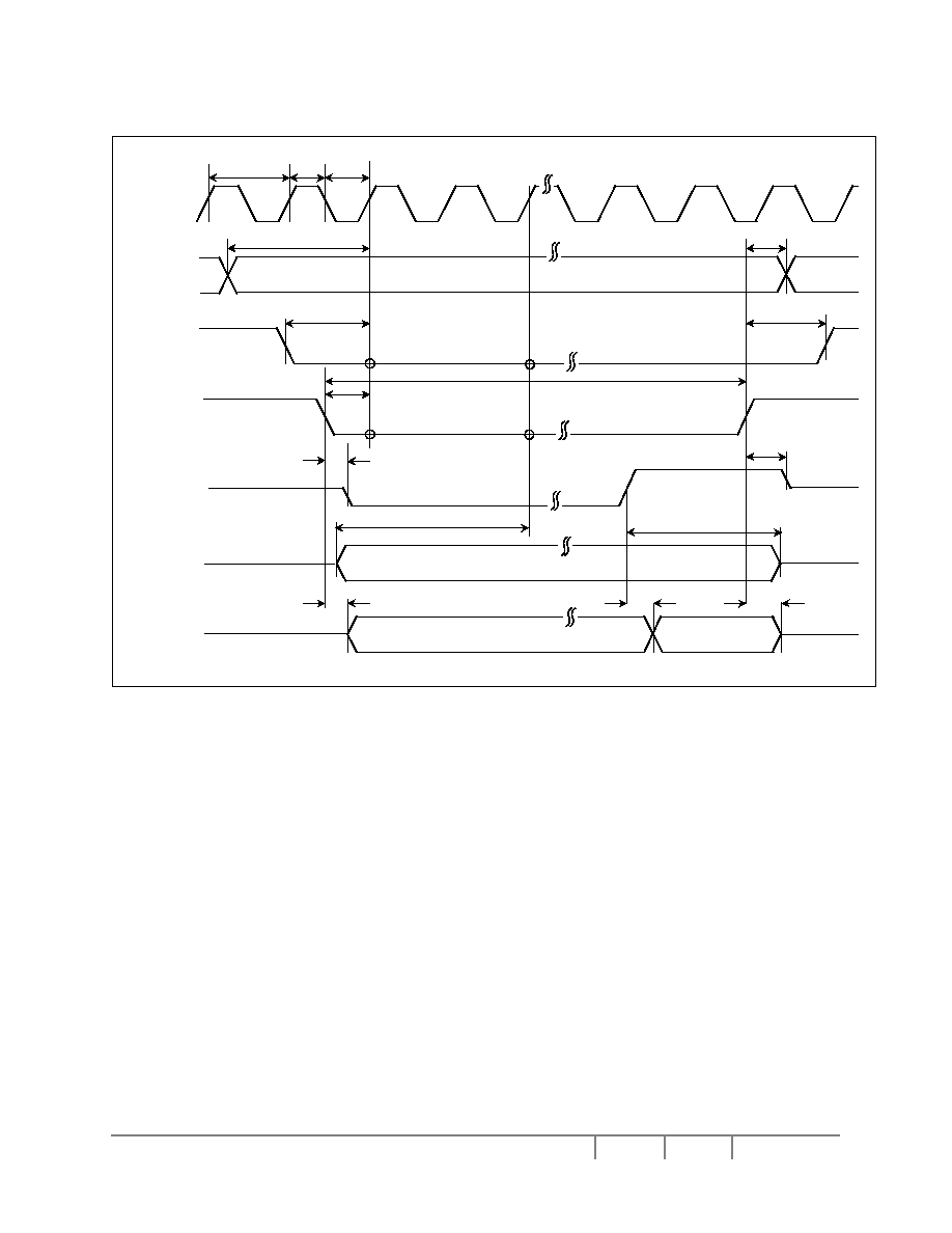
Solomon Systech
Oct 2003 P 66/144
Rev 1.4
SSD1905
10.2.2 Generic #2 Interface Timing (e.g. ISA)
t
13
t
7
t
9
SA[16:0],
M/R#, SBHE#
t
10
BUSCLK
IOCHRDY
MEMR#
MEMW#
CS#
SD[15:0]
(read)
SD[15:0]
(write)
T
BUSCLK
t
2
t
1
t
3
t
4
t
6
t
5
t
15
t
11
t
14
t
12
t
8
VALID
Figure 10-3 : Generic #2 Interface Timing

SSD1905
Rev 1.4
P 67/144 Oct 2003
Solomon Systech
Table 10-5 : Generic #2 Interface Timing
Symbol
Parameter
Min
Max
Units
f
BUSCLK
Bus Clock frequency
66
MHz
T
BUSCLK
Bus Clock period
1/f
BUSCLK
ns
t
1
Clock pulse width high
6
ns
t
2
Clock pulse width low
6
ns
t
3
SA[16:0], M/R#, SBHE# setup to first BUSCLK rising edge
where CS# = 0 and either MEMR# = 0 or MEMW# = 0
1
ns
t
4
SA[16:0], M/R#, SBHE# hold from either MEMR# or MEMW#
rising edge
0
ns
t
5
CS# setup to BUSCLK rising edge
1
ns
t
6
CS# hold from either MEMR# or MEMW# rising edge
0
ns
t
7a
MEMR# or MEMW# asserted for MCLK = BCLK
13
T
BUSCLK
t
7b
MEMR# or MEMW# asserted for MCLK = BCLK
�2
18
T
BUSCLK
t
7c
MEMR# or MEMW# asserted for MCLK = BCLK
�3
23
T
BUSCLK
t
7d
MEMR# or MEMW# asserted for MCLK = BCLK
�4
28
T
BUSCLK
t
8
MEMR# or MEMW# setup to BUSCLK rising edge
1
ns
t
9
Falling edge of either MEMR# or MEMW# to IOCHRDY driven
low
3 15
ns
t
10
Rising edge of either MEMR# or MEMW# to IOCHRDY high
impedance
3 13
ns
t
11
SD[15:0] setup to third BUSCLK rising edge where CS# = 0 and
MEMW#=0 (write cycle)(see note1)
0
ns
t
12
SD[15:0] hold from IOCHRDY rising edge (write cycle)
0
ns
t
13
MEMR# falling edge to SD[15:0] driven (read cycle)
3
13
ns
t
14
IOCHRDY rising edge to SD[15:0] valid (read cycle)
2
ns
t
15
Rising edge of MEMR# to SD[15:0] high impedance (read
cycle)
3 12
ns
1. t
11
is the delay from when data is placed on the bus until the data is latched into the write buffer.
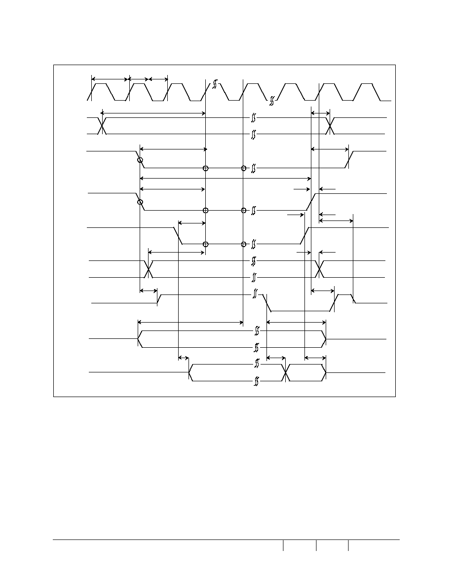
Solomon Systech
Oct 2003 P 68/144
Rev 1.4
SSD1905
10.2.3 Motorola MC68K #1 Interface Timing (e.g. MC68000)
t
19
t
7
t
20
t
11
t
9
A[16:1],
M/R#
UDS#,
LDS#
t
10
CLK
DTACK#
R/W#
AS#
CS#
D[15:0]
(write)
T
CLK
t
2
t
1
t
3
t
4
t
6
t
5
t
15
t
17
t
18
t
14
t
12
t
13
t
16
t
8
D[15:0]
(read)
t
21
VALID
Figure 10-4 : Motorola MC68K #1 Interface Timing
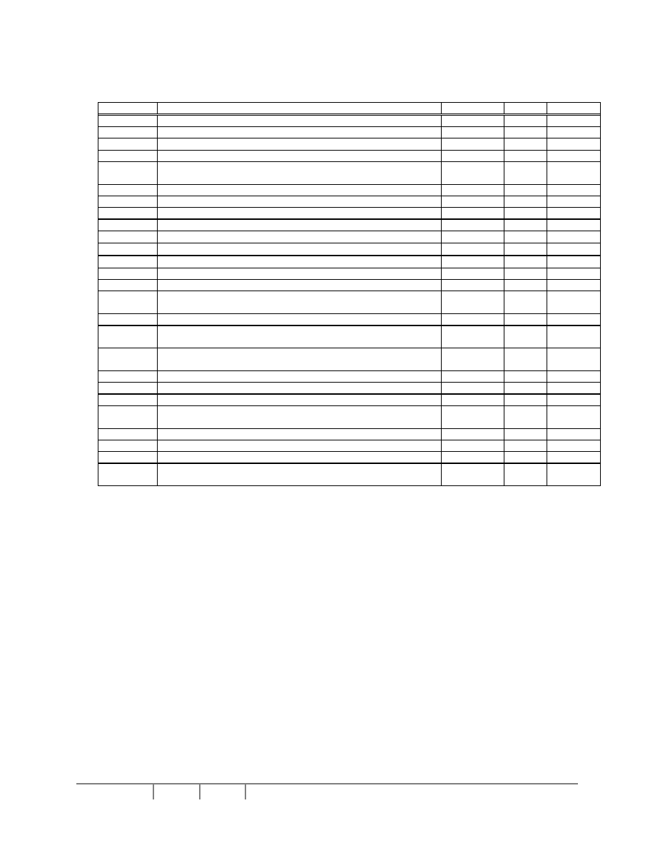
SSD1905
Rev 1.4
P 69/144 Oct 2003
Solomon Systech
Table 10-6 : Motorola MC68K #1 Interface Timing
Symbol
Parameter
Min
Max
Units
f
CLK
Bus Clock frequency
66
MHz
T
CLK
Bus Clock period
1/f
CLK
ns
t
1
Clock pulse width high
6
ns
t
2
Clock pulse width low
6
ns
t
3
A[16:1], M/R# setup to first CLK rising edge where CS# = 0,
AS#=0,UDS#=0,and LDS#=0
1
ns
t
4
A[16:1], M/R# hold from AS# rising edge
0
ns
t
5
CS# setup to CLK rising edge while AS#, UDS#/LDS# = 0
1
ns
t
6
CS# hold from AS# rising edge
0
ns
t
7a
AS# asserted for MCLK = BCLK
13
T
CLK
t
7b
AS# asserted for MCLK = BCLK
�2
18
T
CLK
t
7c
AS# asserted for MCLK = BCLK
�3
23
T
CLK
t
7d
AS# asserted for MCLK = BCLK
�4
28
T
CLK
t
8
AS# setup to CLK rising edge while CS#, AS#, UDS#/LDS# =0
1
ns
t
9
AS# setup to CLK rising edge
2
T
CLK
t
10
UDS#/LDS# setup to CLK rising edge while CS#, AS#,
UDS#/LDS# = 0
1
ns
t
11
UDS#/LDS# high setup to CLK rising edge
2
ns
t
12
First CLK rising edge where AS#=1 to DTACK# high
impedance
3 14
ns
t
13
R/W# setup to CLK rising edge before all CS#, AS#, UDS#
and/or LDS# = 0
1
ns
t
14
R/W# hold from AS# rising edge
0
ns
t
15
AS# = 0 and CS# = 0 to DTACK# driven high
3
13
ns
t
16
AS# rising edge to DTACK# rising edge
4
16
ns
t
17
D[15:0] valid to third CLK rising edge where CS# = 0, AS# = 0
and either UDS# = 0 or LDS# = 0 (write cycle) (see note 1)
0
ns
t
18
D[15:0] hold from DTACK# falling edge (write cycle)
0
ns
t
19
UDS# = 0 and/or LDS# = 0 to D[15:0] driven (read cycle)
3
13
ns
t
20
DTACK# falling edge to D[15:0] valid (read cycle)
2
ns
t
21
UDS#, LDS# rising edge to D[15:0] high impedance (read
cycle)
3 13
ns
1. t
17
is the delay from when data is placed on the bus until the data is latched into the write buffer.
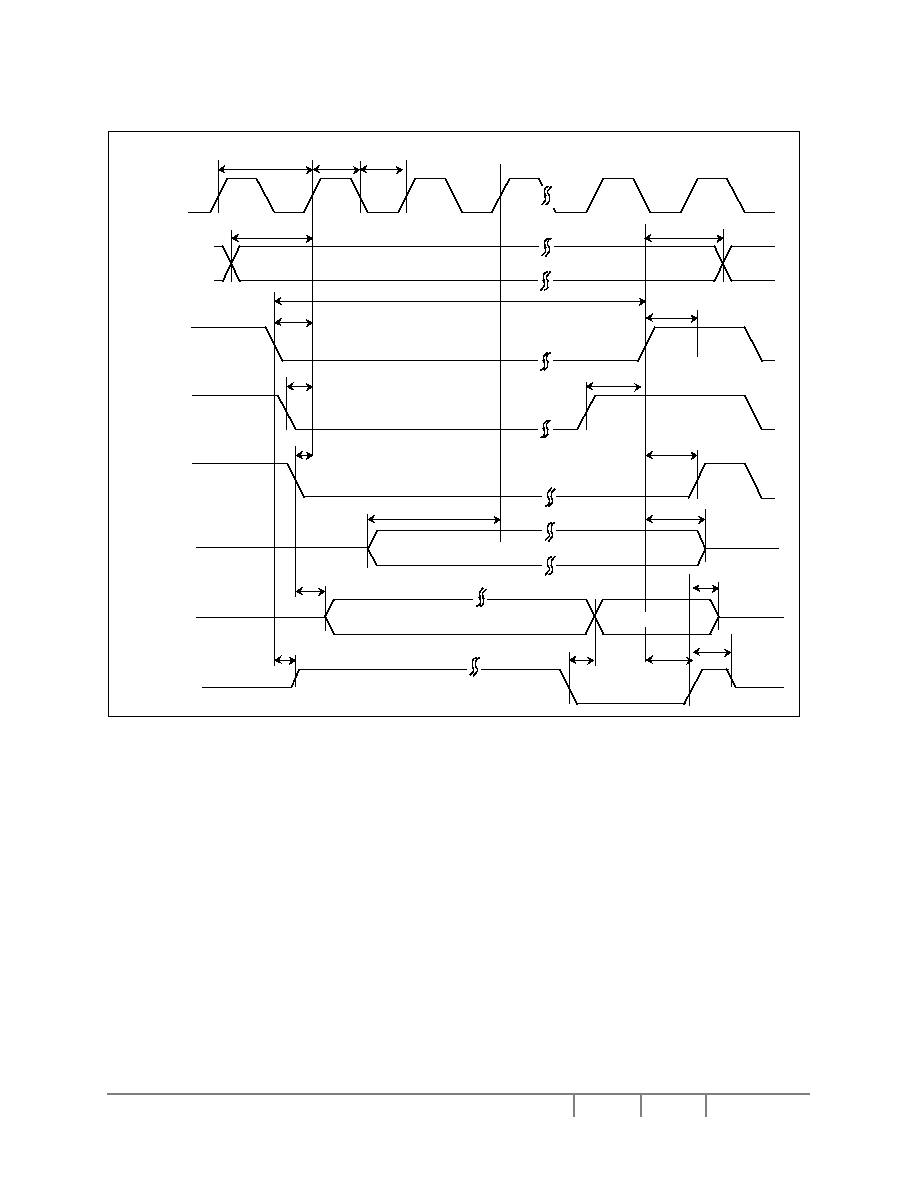
Solomon Systech
Oct 2003 P 70/144
Rev 1.4
SSD1905
10.2.4 Motorola DragonBall Interface Timing with DTACK# (e.g. MC68EZ328/MC68VZ328)
t
3
t
4
t
5
UWE#/LWE#
(write)
t
2
T
CLKO
t
1
t
19
t
7
t
11
t
9
OE#
(read)
t
10
DTACK#
D[15:0]
(read)
D[15:0]
(write)
t
6
t
15
t
17
t
18
t
14
t
12
t
13
t
16
t
8
VALID
Hi-Z
Hi-Z
A[16:1]
Hi-Z
Hi-Z
CSX#
CLKO
Figure 10-5 : Motorola DragonBall Interface with DTACK# Timing
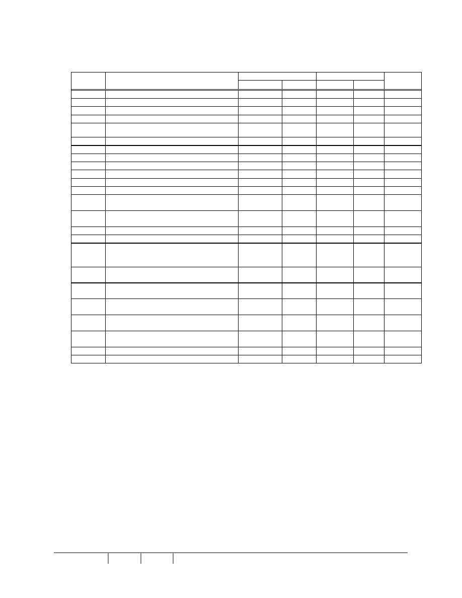
SSD1905
Rev 1.4
P 71/144 Oct 2003
Solomon Systech
Table 10-7 : Motorola DragonBall Interface with DTACK# Timing
Symbol
Parameter
MC68EZ328
MC68VZ328
Units
Min
Max
Min
Max
f
CLKO
Bus Clock frequency
16
33
MHz
T
CLKO
Bus Clock period
1/f
CLKO
1/f
CLKO
ns
t
1
Clock pulse width high
28.1
13.5
ns
t
2
Clock pulse width low
28.1
13.5
ns
t
3
A[16:1] setup 1st CLKO when CSX# = 0 and
either UWE#/LWE# or OE# =0
0 0
ns
t
4
A[16:1] hold from CSX# rising edge
0
0
ns
t
5a
CSX# asserted for MCLK = BCLK
13
13
T
CLKO
t
5b
CSX# asserted for MCLK = BCLK
�2
18
18
T
CLKO
t
5c
CSX# asserted for MCLK = BCLK
�3
23
23
T
CLKO
t
5d
CSX# asserted for MCLK = BCLK
�4
28
28
T
CLKO
t
6
CSX# setup to CLKO rising edge
0 0
ns
t
7
CSX# rising edge to CLKO rising edge
0 0
ns
t
8
UWE#/LWE# falling edge to CLKO rising
edge
0 0
ns
t
9
UWE#/LWE# rising edge to CSX# rising
edge
0 0
ns
t
10
OE# falling edge to CLKO rising edge
1 1
ns
t
11
OE# hold from CSX# rising edge
0 0
ns
t
12
D[15:0] setup to 3rd CLKO when CSX#,
UWE#/LWE# asserted (write cycle) (see
note 1)
0 0
ns
t
13
D[15:0] in hold from CSX# rising
edge(write cycle)
0 0
ns
t
14
Falling edge of OE# to D[15:0] driven
(read cycle)
3 15 3
15
ns
t
15
CLKO rising edge to D[15:0] output Hi-Z
(read cycle)
2 12 2
12
ns
t
16
CSX# falling edge to DTACK# driven
high
3 13 3
13
ns
t
17
DTACK# falling edge to D[15:0]valid
(read cycle)
2
2
ns
t
18
CSX# high to DTACK# high
3 16 3
16
ns
t
19
CLKO rising edge to DTACK# Hi-Z
1 6
1
6
ns
1
t
12
is the delay from when data is placed on the bus until the data is latched into the write buffer.
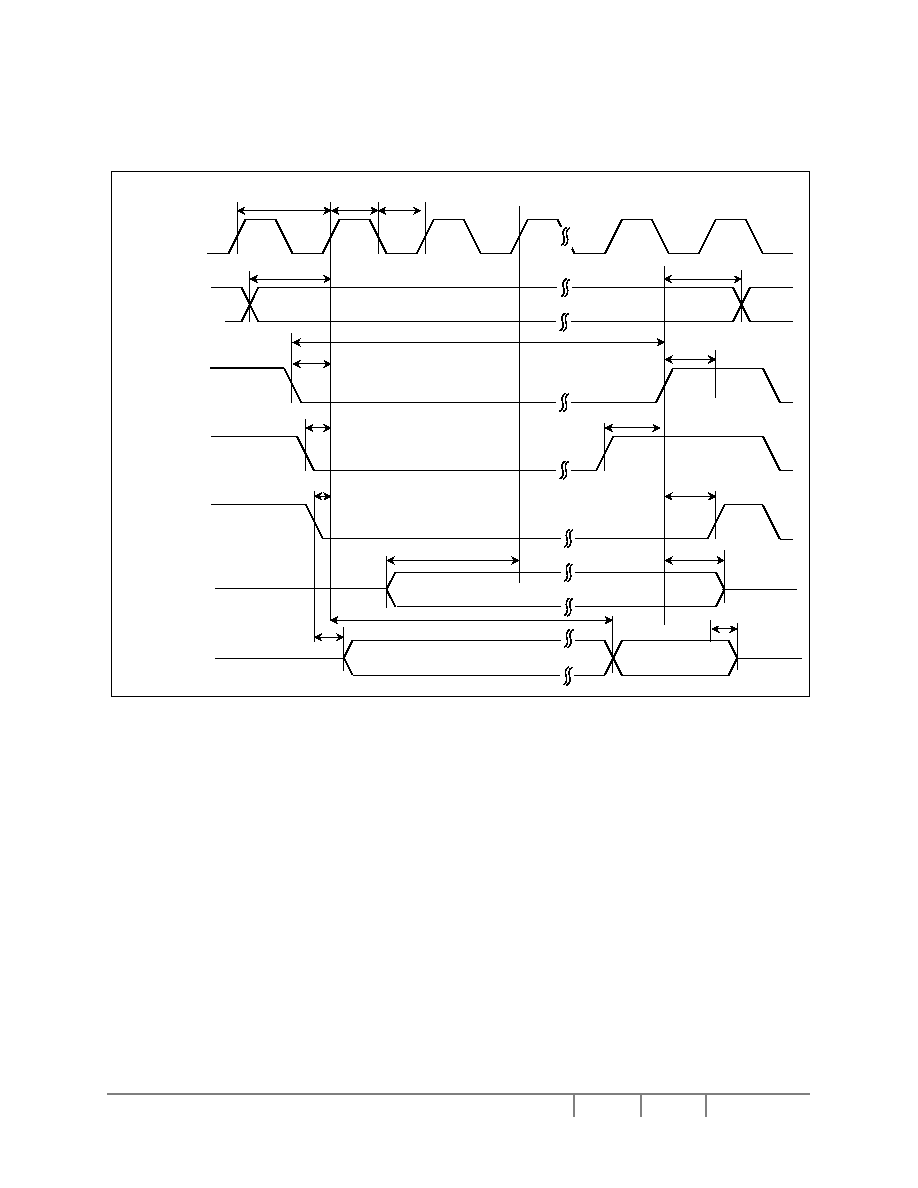
Solomon Systech
Oct 2003 P 72/144
Rev 1.4
SSD1905
10.2.5 Motorola DragonBall Interface Timing without DTACK# (e.g. MC68EZ328/MC68VZ328)
Figure 10-6 : Motorola DragonBall Interface without DTACK# Timing
t
15
t
14
t
10
t
3
t
4
t
5
UWE#/LWE#
(write)
t
2
CLKO
T
CLKO
t
1
t
7
t
11
t
9
OE#
(read)
D[15:0]
(read)
D[15:0]
(write)
t
6
t
12
t
13
t
16
t
8
VALID
Hi-Z
Hi-Z
A[16:1]
Hi-Z
Hi-Z
CSX#
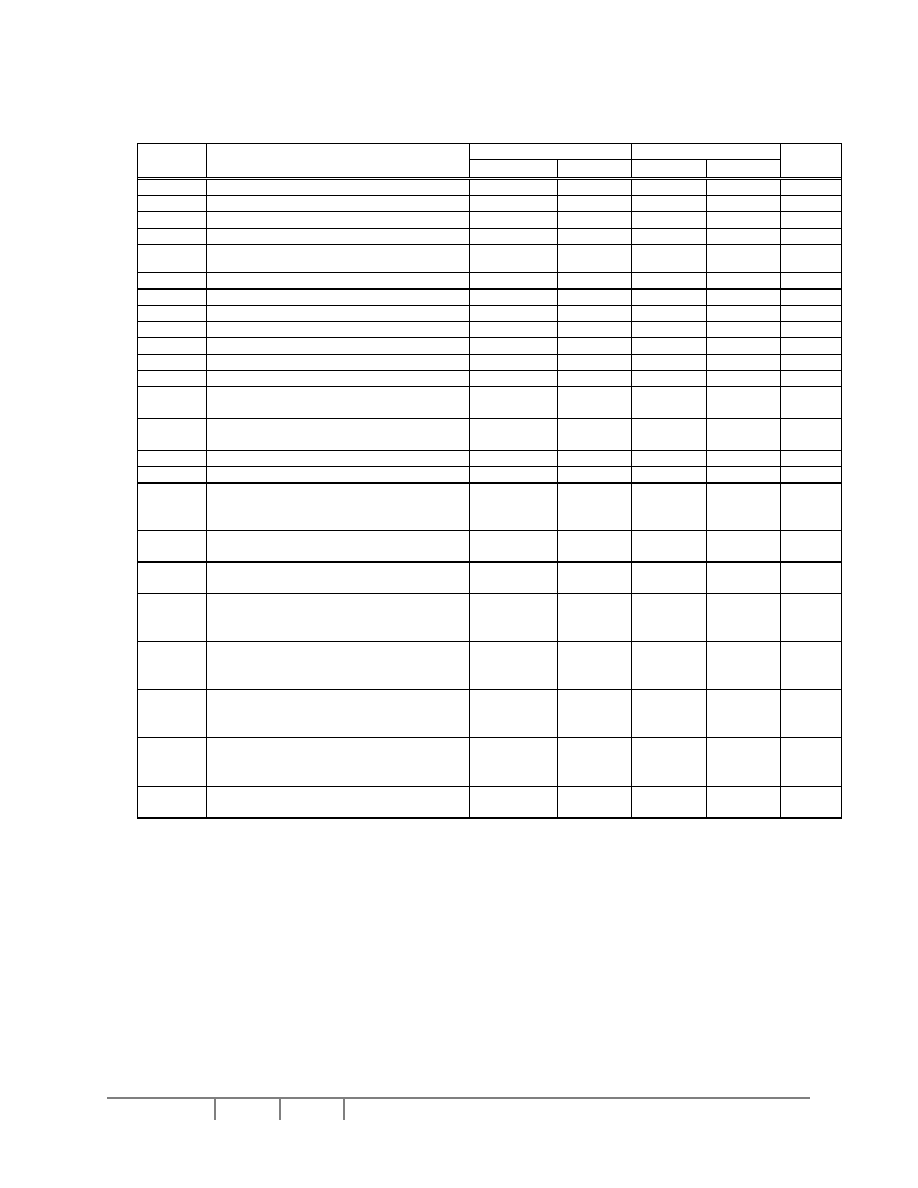
SSD1905
Rev 1.4
P 73/144 Oct 2003
Solomon Systech
Table 10-8 : Motorola DragonBall Interface without DTACK# Timing
Symbol
Parameter
MC68EZ328
MC68VZ328
Units
Min
Max
Min
Max
f
CLKO
Bus Clock frequency
16
33
MHz
T
CLKO
Bus Clock period
1/f
CLKO
1/f
CLKO
ns
t
1
Clock pulse width high
28.1
13.6
ns
t
2
Clock pulse width low
28.1
13.6
ns
t
3
A[16:1] setup 1st CLKO when CSX# = 0 and
either UWE#/LWE# or OE# =0
0
0
ns
t
4
A[16:1] hold from CSX# rising edge
0
0
ns
t
5a
CSX# asserted for MCLK = BCLK
13
13
T
CLKO
t
5b
CSX# asserted for MCLK = BCLK
�2
18
18
T
CLKO
t
5c
CSX# asserted for MCLK = BCLK
�3
23
23
T
CLKO
t
5d
CSX# asserted for MCLK = BCLK
�4
28
28
T
CLKO
t
6
CSX# setup to CLKO rising edge
0
0
ns
t
7
CSX# rising edge to CLKO rising edge
0
0
ns
t
8
UWE#/LWE# falling edge to CLKO rising
edge
0
0
ns
t
9
UWE#/LWE# rising edge to CSX# rising
edge
0
0
ns
t
10
OE# falling edge to CLKO rising edge
1
1
ns
t
11
OE# hold from CSX# rising edge
0
0
ns
t
12
D[15:0] setup to 3rd CLKO when CSX#,
UWE#/LWE# asserted (write cycle) (see
note 1)
0
0
ns
t
13
D[15:0] hold from CSX# rising edge(write
cycle)
0
0
ns
t
14
Falling edge of OE# to D[15:0] driven
(read cycle)
3 15
3 15
ns
t
15a
1st CLKO rising edge after OE# and
CSX# asserted low to D[15:0] valid for
MCLK = BCLK (read cycle)
13
13
T
CLKO
t
15b
1st CLKO rising edge after OE# and
CSX# asserted low to D[15:0] valid for
MCLK = BCLK
�2 (read cycle)
18
18
T
CLKO
t
15c
1st CLKO rising edge after OE# and
CSX# asserted low to D[15:0] valid for
MCLK = BCLK
�3 (read cycle)
23
23
T
CLKO
t
15d
1st CLKO rising edge after OE# and
CSX# asserted low to D[15:0] valid for
MCLK = BCLK
�4 (read cycle)
28
28
T
CLKO
t
16
CLKO rising edge to D[15:0] output Hi-Z
(read cycle)
2 12
2 12
ns
Note
1 t
12
is the delay from when data is placed on the bus until the data is latched into the write buffer.
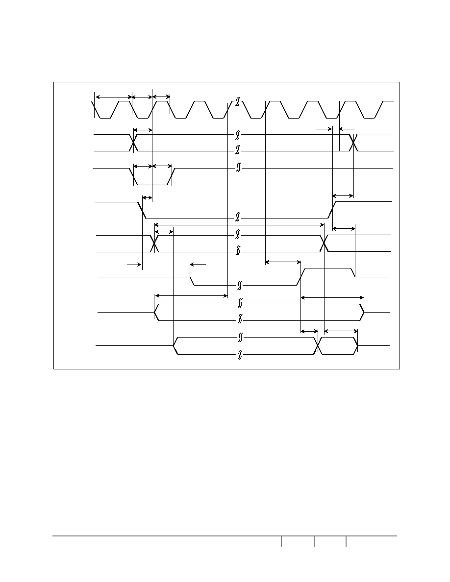
Solomon Systech
Oct 2003 P 74/144
Rev 1.4
SSD1905
t
9
A[16:1], M/R#,
RD/WR#
Hi-Z
t
10
CKIO
WAIT#
WEn#, RD#
CSn#
BS#
D[15:0]
(read)
D[15:0]
(write)
T
CKIO
t
2
t
1
t
3
t
4
t
6
t
5
t
15
t
11
t
17
t
14
t
12
t
13
t
16
t
8
Hi-Z
Hi-Z
Hi-Z
Hi-Z
Hi-Z
t
7
VALID
10.2.6 Hitachi SH-3 Interface Timing (e.g. SH7709A)
Figure 10-7 : Hitachi SH-3 Interface Timing
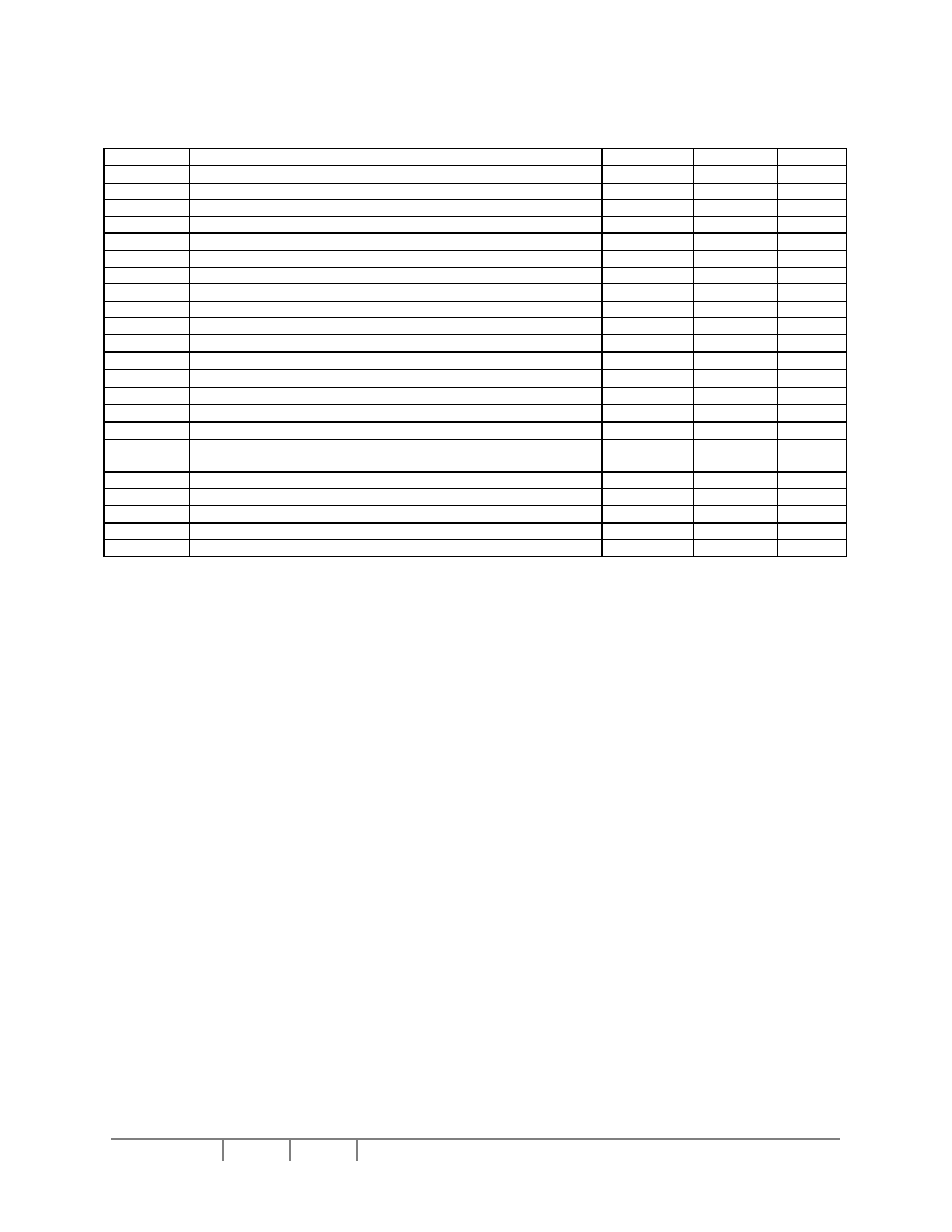
SSD1905
Rev 1.4
P 75/144 Oct 2003
Solomon Systech
Table 10-9 : Hitachi SH-3 Interface Timing
Symbol
Parameter
Min
Max
Units
f
CKIO
Bus Clock frequency
66
MHz
T
CKIO
Bus Clock period
1/f
CKIO
ns
t
1
Bus Clock pulse width low
9
ns
t
2
Bus Clock pulse width high
9
ns
t
3
A[16:1], M/R#, RD/WR# setup to CKIO
1
ns
t
4
CSn# high setup to CKIO
1
ns
t
5
BS# setup
1
ns
t
6
BS# hold
2
ns
t
7
CSn# setup
1
ns
t
8
A[16:1], M/R#, RD/WR# hold from CS#
0
ns
t
9a
RD# or WEn# asserted for MCLK = BCLK (max.MCLK=50MHz)
13
T
CKIO
t
9b
RD# or WEn# asserted for MCLK = BCLK
�2
18
T
CKIO
t
9c
RD# or WEn# asserted for MCLK = BCLK
�3
23
T
CKIO
t
9d
RD# or WEn# asserted for MCLK = BCLK
�4
28
T
CKIO
t
10
Falling edge RD# to D[15:0] driven (read cycle)
3
12
ns
t
11
Rising edge CSn# to WAIT# high impedance
2
10
ns
t
12
Falling edge CSn# to WAIT# driven low
3T
CKIO
+ 2
3T
CKIO
+
12
ns
t
13
CLIO to WAIT# delay
4
18
ns
t
14
D[15:0] setup to 2
nd
CKIO after BS# (write cycle) (see note 1)
0
ns
t
15
D[15:0] hold (write cycle)
0
ns
t
16
WAIT# rising edge to D[15:0] valid (read cycle)
2
ns
t
17
Rising edge RD# to D[15:0] high impedance (read cycle)
3
12
ns
1. t
14
is the delay from when data is placed on the bus until the data is latched into the write buffer.
Note
Minimum three software WAIT state are required.
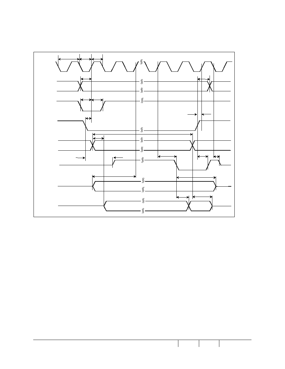
Solomon Systech
Oct 2003 P 76/144
Rev 1.4
SSD1905
10.2.7 Hitachi SH-4 Interface Timing (e.g. SH7751)
Figure 10-8 : Hitachi SH-4 Interface Timing
t
9
A[16:1], M/R#,
RD/WR#
Hi
-
Z
t
10
CKIO
RDY#
WEn#, RD#
CSn#
BS#
D[15:0]
(read)
D[15:0]
(write)
T
CKIO
t
2
t
1
t
3
t
4
t
6
t
5
t
15
t
11
t
17
t
18
t
14
t
12
t
13
t
16
t
8
Hi
-
Z
Hi
-
Z
Hi
-
Z
Hi
-
Z
Hi
-
Z
t
7
VALID

SSD1905
Rev 1.4
P 77/144 Oct 2003
Solomon Systech
Table 10-10 : Hitachi SH-4 Interface Timing
Symbol
Parameter
Min
Max
Units
f
CKIO
Clock frequency
66
MHz
T
CKIO
Clock period
1/f
CKIO
ns
t
1
Clock pulse width low
6.8
ns
t
2
Clock pulse width high
6.8
ns
t
3
A[16:1], M/R#, RD/WR# setup to CKIO
1
ns
t
4
A[16:1], M/R#, RD/WR# hold from CSn#
0
ns
t
5
BS# setup
1
ns
t
6
BS# hold
2
ns
t
7
CSn# setup
1
ns
t
8
CSn# high setup to CKIO
2
ns
t
9a
RD# or WEn# asserted for MCLK = BCLK (max.MCLK=50MHz)
13
T
CKIO
t
9b
RD# or WEn# asserted for MCLK = BCLK
�2
18
T
CKIO
t
9c
RD# or WEn# asserted for MCLK = BCLK
�3
23
T
CKIO
t
9d
RD# or WEn# asserted for MCLK = BCLK
�4
28
T
CKIO
t
10
Falling edge RD# to D[15:0] driven (read cycle)
3
12
ns
t
11
Falling edge CSn# to RDY# driven high
3T
CKIO
+ 3
3T
CKIO
+
12
ns
t
12
CKIO to RDY# low
4
18
ns
t
13
CSn# high to RDY# high
4
14
ns
t
14
Falling edge CKIO to RDY# high impedance
4
14
ns
t
15
D[15:0] setup to 2
nd
CKIO after BS# (write cycle) (see note 1)
0
ns
t
16
D[15:0] hold (write cycle)
0
ns
t
17
RDY# falling edge to D[15:0] valid (read cycle)
2
ns
t
18
Rising edge RD# to D[15:0] high impedance (read cycle)
3
12
ns
1. t
15
is the delay from when data is placed on the bus until the data is latched into the write buffer.
Note
Minimum three software WAIT state are required.
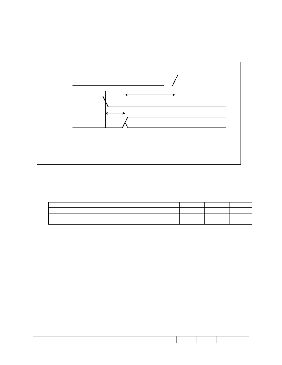
Solomon Systech
Oct 2003 P 78/144
Rev 1.4
SSD1905
10.3 LCD Power Sequencing
10.3.1 Passive/TFT Power-On Sequence
Figure 10-9 : Passive/TFT Power-On Sequence Timing
Table 10-11 : Passive/TFT Power-On Sequence Timing
Symbol Parameter
Min
Max Units
t
1
LCD signals active to LCD bias active
Note 1
Note 1
t
2
Power Saving Mode disabled to LCD signals
active
0 20 ns
1. t
1
is controlled by software and must be determined from the bias power supply delay requirements of the
panel connected.
Note
For HR-TFT Power-On/Off sequence information, see referenced document of Sharp HR-TFT Panels.
Power Saving
Mode Enable**
(REG[A0h] bit 0)
LCD Signals***
*It is recommended to use the general purpose output pin GPO to control the LCD bias power.
**The LCD power-on sequence is activated by programming the Power Saving Mode Enable bit (REG[A0h] bit 0) to 0.
***LCD Signal include: LDATA[17:0], LSHIFT, LLINE, LFRAME, and LDEN.
GPO*
t
2
t
1
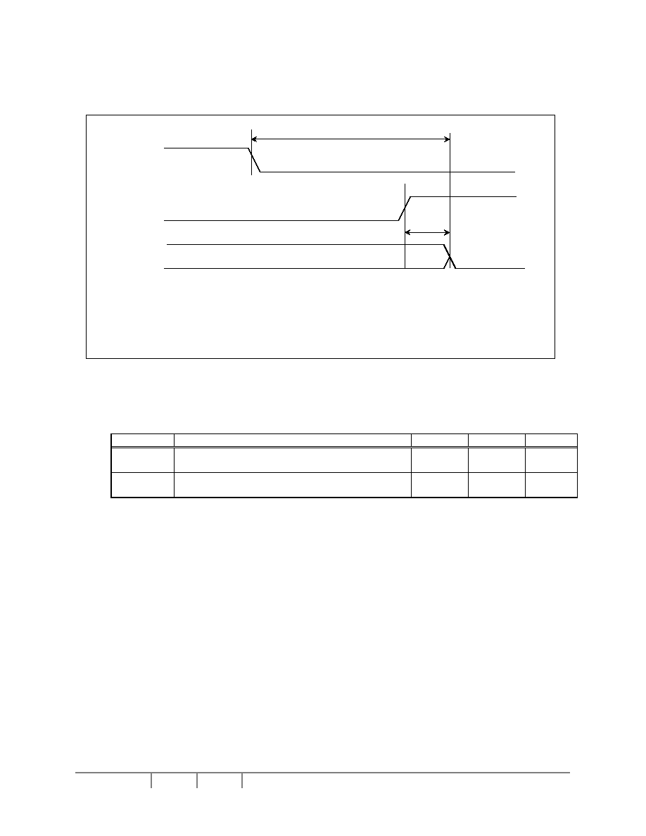
SSD1905
Rev 1.4
P 79/144 Oct 2003
Solomon Systech
10.3.2 Passive/TFT Power-Off Sequence
Figure 10-10 : Passive/TFT Power-Off Sequence Timing
Table 10-12 : Passive/TFT Power-Off Sequence Timing
Symbol Parameter
Min
Max Units
t
1
LCD bias deactivated active to LCD signals
inactive
Note 1
Note 1
t
2
Power Saving Mode disabled to LCD signals
low
0 20 ns
1. t
1
is controlled by software and must be determined from the bias power supply delay requirements of the panel
connected.
*It is recommended to use the general purpose output pin GPO to control the LCD bias power.
**The LCD power-off sequence is activated by programming the Power Saving Mode Enable bit (REG[A0h] bit 0) to 1.
***LCD Signal include: LDATA[17:0], LSHIFT, LLINE, LFRAME, and LDEN.
Power Saving
Mode Enable**
(REG[A0h] bit 0)
LCD Signals***
GPO*
t
2
t
1
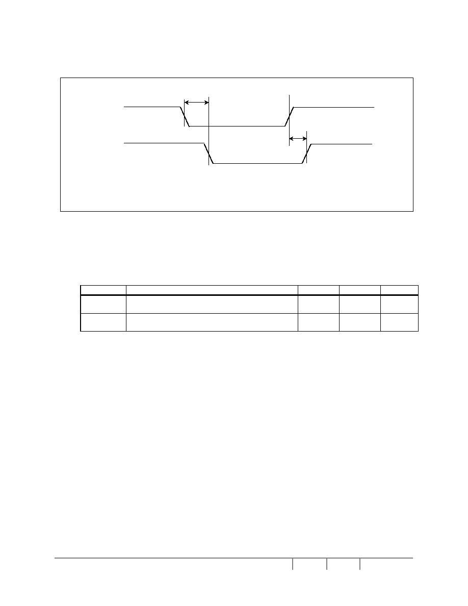
Solomon Systech
Oct 2003 P 80/144
Rev 1.4
SSD1905
10.3.3 Power Saving Status
Figure 10-11 : Power Saving Status Timing
Table 10-13 : Power Saving Status Timing
Symbol Parameter
Min
Max Units
t
1
Power Saving Mode disabled to Memory
Controller Power Saving Status low
Note 1
Note 1
ns
t
2
Power Saving Mode enabled to Memory
Controller Power Saving Status high
0 20 MCLK
(note 1)
1. For further information on the internal clock MCLK, see Section11.1.2, "MCLK".
Memory Controller
Power Saving Status**
Power Saving
Mode Enable*
(REG[A0h] bit 0)
t
2
t
1
* Power Saving Mode is controlled by the Power Saving Mode Enable bit (REG[A0h] bit 0).
** Memory Controller Power Saving Status is controlled by the Memory Controller Power Saving Status bit (REG[A0h] bit3).
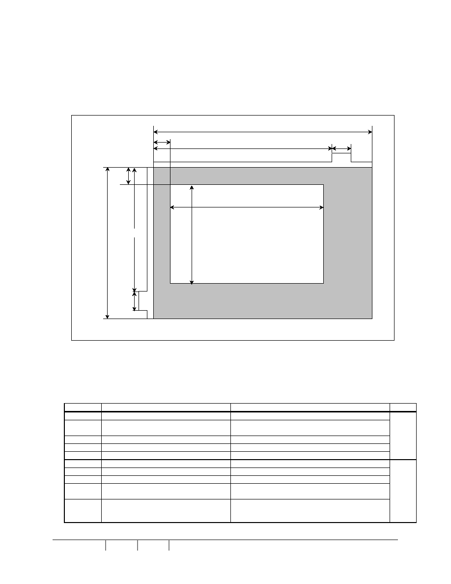
SSD1905
Rev 1.4
P 81/144 Oct 2003
Solomon Systech
10.4 Display Interface
Figure 10-12 :
Panel Timing Parameters
shows the timing parameters required to drive a flat panel display.
Timing details for each supported panel types are provided in the remainder of this section.
Figure 10-12 :
Panel Timing Parameters
Table 10-14 : Panel Timing Parameter Definition and Register Summary
Symbol
Description
Derived From
Units
HT
Horizontal Total
((REG[12h] bits 6-0) + 1) x 8
HDP
2
Horizontal Display Period
2
((REG[14h] bits 6-0) + 1) x 8
HDPS
3
Horizontal Display Period Start Position
3
((REG[17h]bits1-0,REG[16h]bits7-0)+ Offset
5
)
HPS
LLINE Pulse Start Position
(REG[23h] bits 1-0, REG[22h] bits 7-0) + 1
HPW
LLINE Pulse Width
(REG[20h] bits 6-0) + 1
Ts
1
VT
Vertical Total
((REG[19h] bits 1-0, REG[18h] bits 7-0) + 1) x HT
VDP
4
Vertical Display Period
4
((REG[1Dh] bits 1-0, REG[1Ch] bits 7-0) + 1) x HT
VDPS
Vertical Display Period Start Position
(REG[1Fh] bits 1-0, REG[1Eh] bits 7-0) x HT
VPS
LFRAME Pulse Start Position
(REG[27h] bits 1-0, REG[26h] bits 7-0) x HT +
(REG[31h] bits 1-0, REG[30h] bits 7-0)
VPW
LFRAME Pulse Width
((REG[24h] bits 2-0) + 1) x HT + (REG[35h] bits 1-
0, REG[34h] bits 7-0) � (REG[31h] bits 1-0,
REG[30h] bits 7-0)
Ts
1
HPW
VT
VDPS
HDPS
HDP
HT
HPS
VDP
VPS
VPW
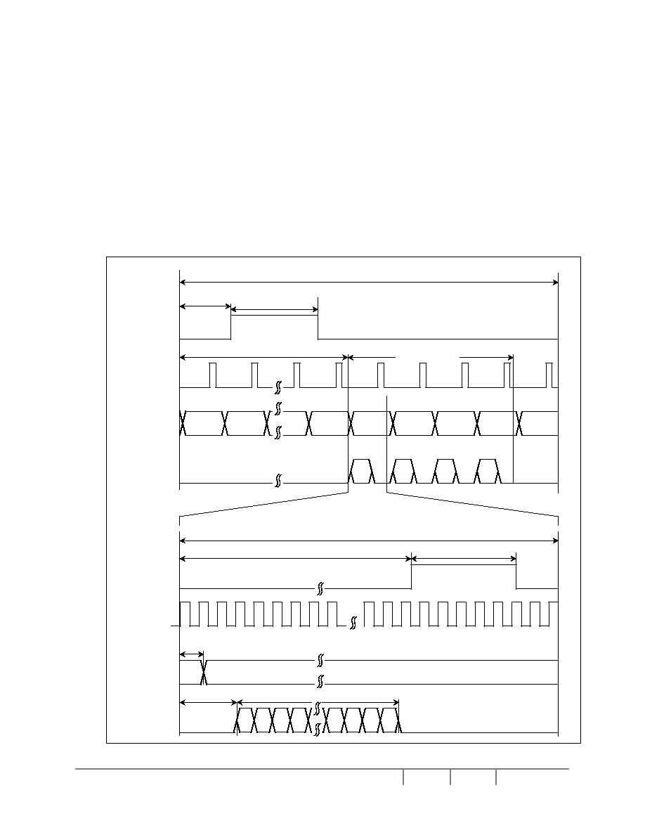
Solomon Systech
Oct 2003 P 82/144
Rev 1.4
SSD1905
The following conditions must be fulfilled for all panel timings:
HDPS + HDP < HT
For passive LCD interface : VDPS + VDP + 1 < VT
For other LCD interface : VDPS + VDP < VT
1
Ts = pixel clock period
2
The HDP must be a minimum of 32 pixels and can be increased by multiples of 8.
3
The HDPS parameter contains an offset that depends on the panel type. This offset is the constant in the
equation to describes parameter t
14
min in the AC Timing tables for the various panel types.
4
The VDP must be a minimum of 2 lines.
5
Offset for STN and CSTN panel = 22, offset for TFT panel = 5.
10.4.1 Generic STN Panel Timing
HDP
HDPS
1PCLK
HT (= 1 Line)
VT (= 1 Frame)
VPW
VPS
VDPS
VDP
HPS
HPW
LFRAME
LLINE
MOD (LDEN)
LDATA[17:0]
LLINE
MOD (LDEN)
LDATA[17:0]
LSHIFT

SSD1905
Rev 1.4
P 83/144 Oct 2003
Solomon Systech
Figure 10-13 :
Generic STN Panel Timing
VT
= Vertical Total
= [(REG[19h]bits1-0,REG[18h]bits7-0)+ 1] lines
VPS = LFRAME Pulse Start Position
= [(REG[27h] bits 1-0, REG[26h] bits 7-0)] x HT + (REG[31h] bits 1-0, REG[30h] bits 7-0) pixels
VPW = LFRAME Pulse Width
= [(REG[24h] bits 2-0) + 1] x HT + (REG[35h] bits 1-0, REG[34h] bits 7-0) � (REG[31h] bits 1-0, REG[30h]
bits 7-0) pixels
VDPS = Vertical Display Period Start Position
= [(REG[1Fh]bits1-0,REG[1Eh]bits7-0)] lines
VDP
= Vertical Display Period
= [(REG[1Dh] bits 1-0, REG[1Ch] bits 7-0) + 1] lines
* The VDP must be a minimum of 2 lines
HT
= Horizontal Total
= [((REG[12h] bits 6-0) + 1) x 8] pixels
HPS = LLINE Pulse Start Position
= [(REG[23h] bits 1-0, REG[22h] bits 7-0) + 1] pixels
HPW = LLINE Pulse Width
= [(REG[20h] bits 6-0) + 1] pixels
HDPS = Horizontal Display Period Start Position
= [(REG[17h]bits1-0,REG[16h]bits7-0)+ 22] pixels
HDP = Horizontal Display Period
= [((REG[14h] bits 6-0) + 1) x 8] pixels
The HDP must be a minimum of 32 pixels and can be increased by multiples of 8.
*Panel Type Bits (REG[10h] bits 1-0) = 00b (STN)
*LFRAME Pulse Polarity Bit (REG[24h] bit 7) = 1 (active high)
*LLINE Polarity Bit (REG[20h] bit 7) = 1 (active high).
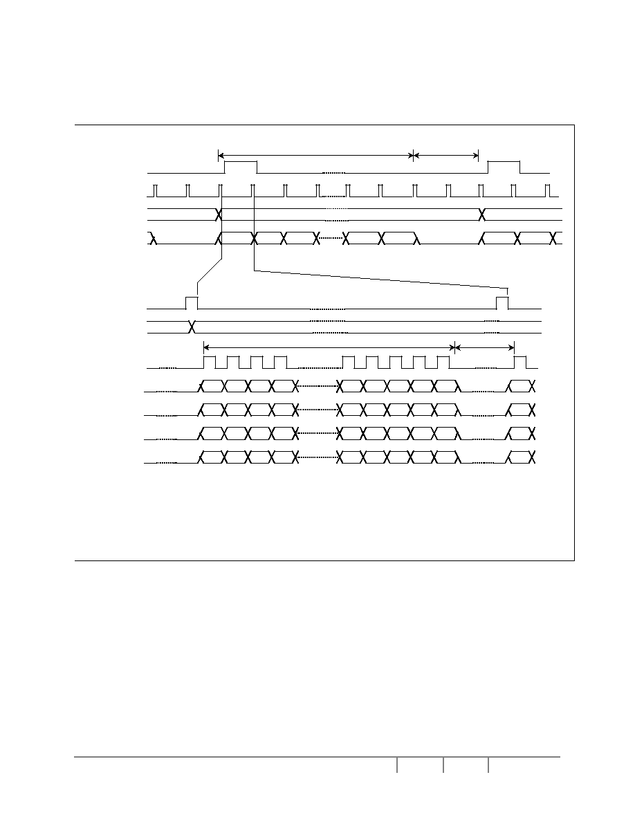
Solomon Systech
Oct 2003 P 84/144
Rev 1.4
SSD1905
10.4.2 Monochrome 4-Bit Panel Timing
LDEN (MOD)
LINE239
LINE2
LINE1
LINE240
LINE3
LINE2
LINE1
1-320
1-319
1-318
1-317
1-8
1-7
1-6
1-4
1-3
1-2
1-5
1-1
LFRAME
LLINE
LDATA[7:4]
LLINE
LSHIFT
LDEN (MOD)
LDATA7
LDATA6
LDATA5
LDATA4
VDP
VNDP
HDP
HNDP
*Diagram drawn with 2 LLINE vertical blank period
Example timing for a 320x240 panel
Figure 10-14 :
Monochrome 4-Bit Panel Timing
VDP = Vertical Display Period
= (REG[1Dh] bits 1:0, REG[1Ch] bits 7:0) + 1 Lines
VNDP = Vertical Non-Display Period
= VT -VDP
= (REG[19h] bits 1:0, REG[18h] bits 7:0) - (REG[1Dh] bits 1:0, REG[1Ch] bits 7:0) Lines
HDP
= Horizontal Display Period
= ((REG[14h] bits 6:0) + 1) x 8Ts
HNDP = Horizontal Non-Display Period
= HT - HDP
= (((REG[12h] bits 6:0) + 1) x 8Ts) - (((REG[14h] bits 6:0) + 1) x 8Ts)

SSD1905
Rev 1.4
P 85/144 Oct 2003
Solomon Systech
t
14
t
13
t
12
t
11
t
10
t
9
t
8
t
7
t
6
t
5
t
4
t
3
Sync Timing
Data Timing
LFRAME
LLINE
LDEN (MOD)
LLINE
LSHIFT
LDATA[7:4]
t
1
t
2
1
2
Figure 10-15 :
Monochrome 4-Bit Panel A.C. Timing

Solomon Systech
Oct 2003 P 86/144
Rev 1.4
SSD1905
Table 10-15 : Monochrome 4-Bit Panel A.C. Timing
Symbol
Parameter
Min
Typ
Max
Units
t
1
LFRAME setup to LLINE falling edge
note 2
Ts (note 1)
t
2
LFRAME hold from LLINE falling edge
note 3
Ts
t
3
LLINE period
note 4
Ts
t
4
LLINE pulse width
note 5
Ts
t
5
MOD transition to LLINE falling edge
note 6
Ts
t
6
LSHIFT falling edge to LLINE rising edge
note 7
Ts
t
7
LSHIFT falling edge to LLINE falling edge
t
6
+ t
4
Ts
t
8
LLINE falling edge to LSHIFT falling edge
t
14
+ 2
Ts
t
9
LSHIFT period
4
Ts
t
10
LSHIFT pulse width low
2
Ts
t
11
LSHIFT pulse width high
2
Ts
t
12
LDATA[7:4] setup to LSHIFT falling edge
2
Ts
t
13
LDATA[7:4] hold from LSHIFT falling edge
2
Ts
t
14
LLINE falling edge to LSHIFT rising edge
note 8
Ts
1. Ts = pixel clock period
2. t
1
min
= (HPS+ HPW) � (REG[31h] bits 1-0, REG[30h] bits 7-0)
3. t
2
min
= VPW - t
1
min
4. t
3
min
= HT
5. t
4
min
= HPW
6. t
5
min
= HT - HPS
7. t
6
min
= HPS - (HDP + HDPS - 2)
if negative add t
3
min
8. t
14
min
= HDPS - (HPS + t
4
min
)
if negative add t
3
min
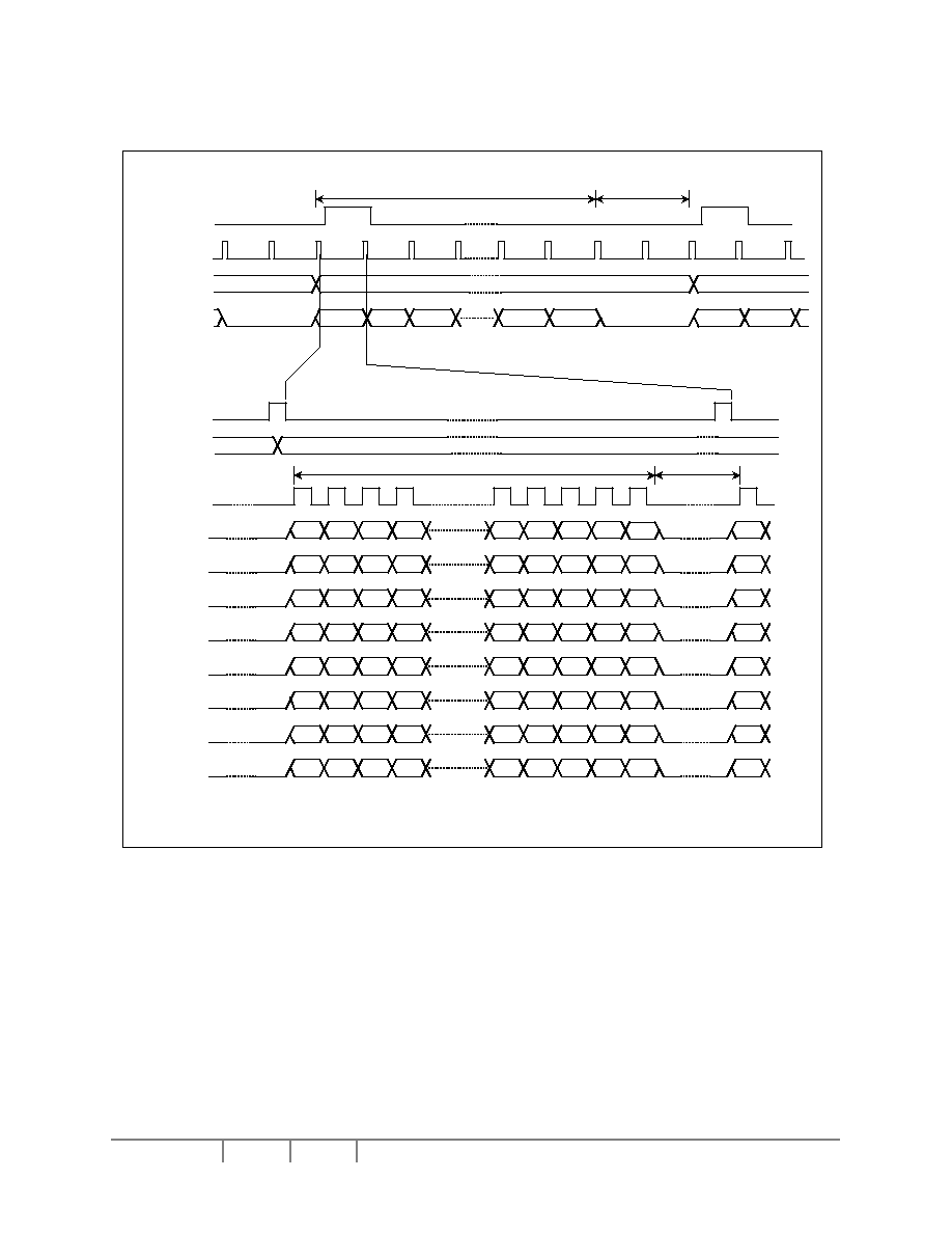
SSD1905
Rev 1.4
P 87/144 Oct 2003
Solomon Systech
10.4.3 Monochrome 8-Bit Panel Timing
LDEN (MOD)
LINE479
LINE2
LINE1
LINE480
LINE3
LINE2
LINE1
1-640
1-639
1-638
1-637
1-636
1-635
1-634
1-633
1-16
1-15
1-14
1-13
1-12
1-11
1-10
1-8
1-6
1-7
1-5
1-4
1-3
1-2
1-9
1-1
LFRAME
LLINE
LDATA[7:0]
LLINE
LSHIFT
LDEN (MOD)
LDATA7
LDATA6
LDATA5
LDATA3
LDATA4
LDATA2
LDATA1
LDATA0
VDP
VNDP
HDP
HNDP
*Diagram drawn with 2 LLINE vertical blank period
Example timing for a 640x480 panel
Figure 10-16 :
Monochrome 8-Bit Panel Timing
VDP = Vertical Display Period
= (REG[1Dh] bits 1:0, REG[1Ch] bits 7:0) + 1 Lines
VNDP = Vertical Non-Display Period
= VT-VDP
= (REG[19h] bits 1:0, REG[18h] bits 7:0) - (REG[1Dh] bits 1:0, REG[1Ch] bits 7:0) Lines
HDP = Horizontal Display Period
= ((REG[14h] bits 6:0) + 1) x 8Ts
HNDP = Horizontal Non-Display Period
= HT - HDP
= (((REG[12h] bits 6:0) + 1) x 8Ts) - (((REG[14h] bits 6:0) + 1) x 8Ts)
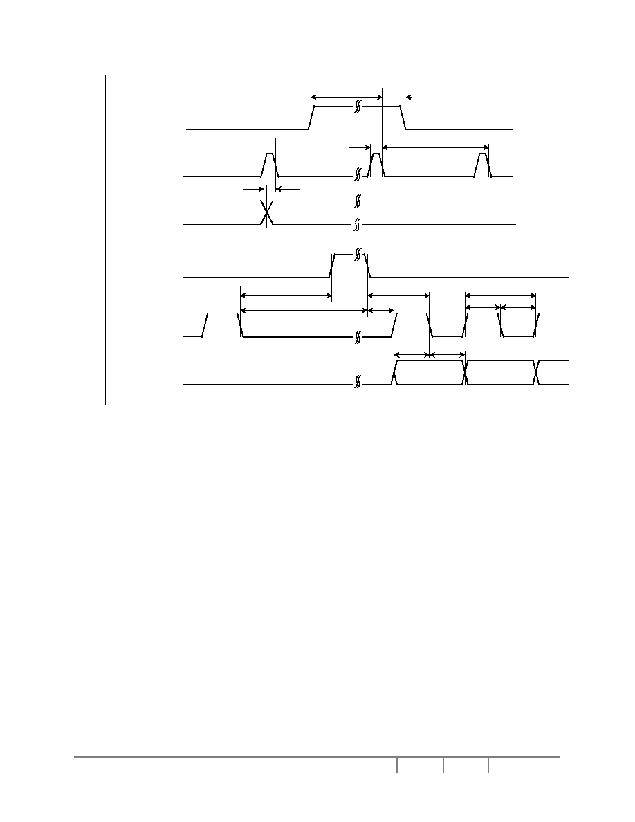
Solomon Systech
Oct 2003 P 88/144
Rev 1.4
SSD1905
t
14
t
13
t
12
t
11
t
10
t
9
t
8
t
7
t
6
t
5
t
4
t
3
Sync Timing
Data Timing
LFRAME
LLINE
LDEN (MOD)
LLINE
LSHIFT
LDATA[7:0]
t
1
t
2
1
2
Figure 10-17 :
Monochrome 8-Bit Panel A.C. Timing
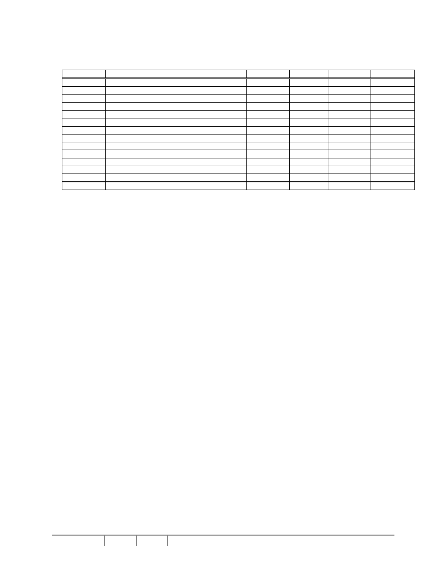
SSD1905
Rev 1.4
P 89/144 Oct 2003
Solomon Systech
Table 10-16 : Monochrome 8-Bit Panel A.C. Timing
Symbol
Parameter
Min
Typ
Max
Units
t
1
LFRAME setup to LLINE falling edge
note 2
Ts (note 1)
t
2
LFRAME hold from LLINE falling edge
note 3
Ts
t
3
LLINE period
note 4
Ts
t
4
LLINE pulse width
note 5
Ts
t
5
MOD transition to LLINE falling edge
note 6
Ts
t
6
LSHIFT falling edge to LLINE rising edge
note 7
Ts
t
7
LSHIFT falling edge to LLINE falling edge
t
6
+ t
4
Ts
t
8
LLINE falling edge to LSHIFT falling edge
t
14
+ 4
Ts
t
9
LSHIFT period
8
Ts
t
10
LSHIFT pulse width low
4
Ts
t
11
LSHIFT pulse width high
4
Ts
t
12
LDATA[7:0] setup to LSHIFT falling edge
4
Ts
t
13
LDATA[7:0] hold from LSHIFT falling edge
4
Ts
t
14
LLINE falling edge to LSHIFT rising edge
note 8
Ts
1. Ts = pixel clock period
2. t
1
min
= (HPS+ HPW) � (REG[31h] bits 1-0, REG[30h] bits 7-0)
3. t
2
min
= VPW - t
1
min
4. t
3
min
= HT
5. t
4
min
= HPW
6. t
5
min
= HT - HPS
7. t
6
min
= HPS - (HDP + HDPS - 4)
if negative add t
3
min
8. t
14
min
= HDPS - (HPS + t
4
min
)
if negative add t
3
min
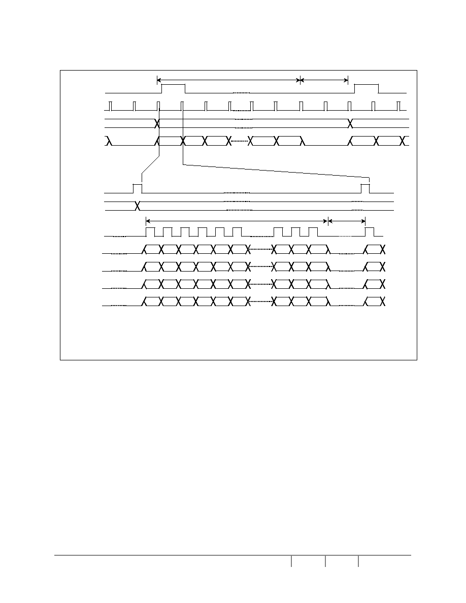
Solomon Systech
Oct 2003 P 90/144
Rev 1.4
SSD1905
10.4.4 Color 4-Bit Panel Timing
1-B4
1-G4
1-R4
1-B3
LDEN (MOD)
LINE239
LINE2
LINE1
LINE240
LINE3
LINE2
LINE1
1-B320
1-G320
1-R320
1-B319
1-G3
1-R3
1-B2
1-R2
1-B1
1-G1
1-G2
1-R1
LFRAME
LLINE
LDATA[7:4]
LLINE
LSHIFT
LDEN (MOD)
LDATA7
LDATA6
LDATA5
LDATA4
VDP
VNDP
HDP
HNDP
*Diagram drawn with 2 LLINE vertical blank period
Example timing for a 320x240 panel
Figure 10-18 :
Color 4-Bit Panel Timing
VDP = Vertical Display Period
= (REG[1Dh] bits 1:0, REG[1Ch] bits 7:0) + 1 Lines
VNDP = Vertical Non-Display Period
= VT-VDP
= (REG[19h] bits 1:0, REG[18h] bits 7:0) - (REG[1Dh] bits 1:0, REG[1Ch] bits 7:0) Lines
HDP = Horizontal Display Period
= ((REG[14h] bits 6:0) + 1) x 8Ts
HNDP = Horizontal Non-Display Period
= HT - HDP
(((REG[12h] bits 6:0) + 1) x 8Ts) - (((REG[14h] bits 6:0) + 1) x 8Ts)

SSD1905
Rev 1.4
P 91/144 Oct 2003
Solomon Systech
t
14
t
13
t
12
t
11
t
10
t
9
t
8
t
7
t
6
t
5
t
4
t
3
Sync Timing
Data Timing
LFRAME
LLINE
LDEN (MOD)
LLINE
LSHIFT
LDATA[7:4]
t
1
t
2
1
2
Figure 10-19 :
Color 4-Bit Panel A.C. Timing
Solomon Systech
Oct 2003 P 92/144
Rev 1.4
SSD1905
Table 10-17 : Color 4-Bit Panel A.C. Timing
Symbol
Parameter
Min
Typ
Max
Units
t
1
LFRAME setup to LLINE falling edge
note 2
Ts (note 1)
t
2
LFRAME hold from LLINE falling edge
note 3
Ts
t
3
LLINE period
note 4
Ts
t
4
LLINE pulse width
note 5
Ts
t
5
MOD transition to LLINE falling edge
note 6
Ts
t
6
LSHIFT falling edge to LLINE rising edge
note 7
Ts
t
7
LSHIFT falling edge to LLINE falling edge
t
6
+ t
4
Ts
t
8
LLINE falling edge to LSHIFT falling edge
t
14
+ 0.5
Ts
t
9
LSHIFT period
2
Ts
t
10
LSHIFT pulse width low
1
Ts
t
11
LSHIFT pulse width high
1
Ts
t
12
LDATA[7:4] setup to LSHIFT falling edge
1
Ts
t
13
LDATA[7:4] hold from LSHIFT falling edge
1
Ts
t
14
LLINE falling edge to LSHIFT rising edge
note 8
Ts
1. Ts = pixel clock period
2. t
1
min
= (HPS+ HPW) � (REG[31h] bits 1-0, REG[30h] bits 7-0)
3. t
2
min
= VPW - t
1
min
4. t
3
min
= HT
5. t
4
min
= HPW
6. t
5
min
= HT - HPS
7. t
6
min
= HPS - (HDP + HDPS - 3)
if negative add t
3
min
8. t
14
min
= HDPS - (HPS + t
4
min
) + 1
if negative add t
3
min
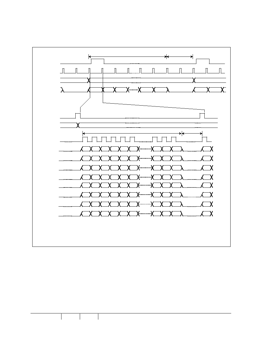
SSD1905
Rev 1.4
P 93/144 Oct 2003
Solomon Systech
10.4.5 Color 8-Bit Panel Timing (Format stripe)
1-G7
1-R7
1-B6
1-G6
LDEN (MOD)
LINE479
LINE2
LINE1
LINE480
LINE3
LINE2
LINE1
1-G639
1-R639
1-B638
1-G638
1-B4
1-G4
1-R4
1-R2
1-B1
1-G1
1-B3
1-R1
LFRAME
LLINE
LDATA[7:0]
LLINE
LSHIFT
LDEN (MOD)
LDATA7
LDATA6
LDATA5
LDATA4
VDP
VNDP
HDP
HNDP
*Diagram drawn with 2 LLINE vertical blank period
Example timing for a 640X480 panel
1-B8
1-G8
1-R8
1-B7
1-B640
1-G640
1-R640
1-B639
1-R6
1-B5
1-G5
1-G3
1-R3
1-B2
1-R5
1-G2
LDATA3
LDATA2
LDATA1
LDATA0
Figure 10-20 :
Color 8-Bit Panel Timing (Format stripe)
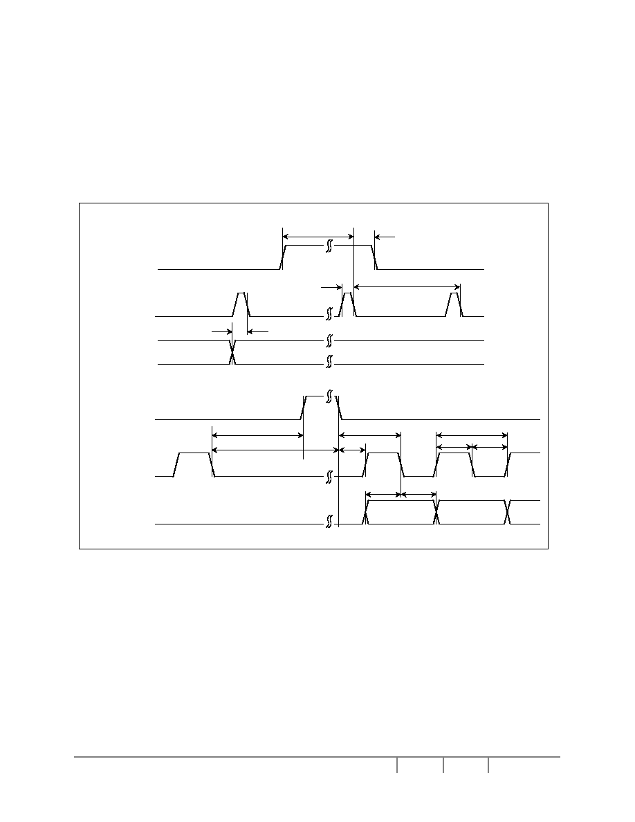
Solomon Systech
Oct 2003 P 94/144
Rev 1.4
SSD1905
VDP = Vertical Display Period
= (REG[1Dh] bits 1:0, REG[1Ch] bits 7:0) + 1 Lines
VNDP = Vertical Non-Display Period
= VT-VDP
= (REG[19h] bits 1:0, REG[18h] bits 7:0) - (REG[1Dh] bits 1:0, REG[1Ch] bits 7:0) Lines
HDP = Horizontal Display Period
= ((REG[14h] bits 6:0) + 1) x 8Ts
HNDP = Horizontal Non-Display Period
= HT - HDP
= (((REG[12h] bits 6:0) + 1) x 8Ts) - (((REG[14h] bits 6:0) + 1) x 8Ts)
t
5
t
4
t
3
Sync Timing
Data Timing
LFRAME
LLINE
LLINE
t
1
t
2
LDEN (MOD)
t
14
t
13
t
12
t
11
t
10
t
9
t
8
t
7
t
6
LSHIFT
LDATA[7:0]
1
2
Figure 10-21 :
Color 8-Bit Panel A.C. Timing (Format stripe)

SSD1905
Rev 1.4
P 95/144 Oct 2003
Solomon Systech
Table 10-18 : Color 8-Bit Panel A.C. Timing (Format stripe)
Symbol
Parameter
Min
Typ
Max
Units
t
1
LFRAME setup to LLINE falling edge
note 2
Ts (note 1)
t
2
LFRAME hold from LLINE falling edge
note 3
Ts
t
3
LLINE period
note 4
Ts
t
4
LLINE pulse width
note 5
Ts
t
5
MOD transition to LLINE falling edge
note 6
Ts
t
6
LSHIFT falling edge to LLINE rising edge
note 7
Ts
t
7
LSHIFT falling edge to LLINE falling edge
t
6
+ t
4
Ts
t
8
LLINE falling edge to LSHIFT falling edge
t
14
+ 2
Ts
t
9
LSHIFT period
2
Ts
t
10
LSHIFT pulse width low
1
Ts
t
11
LSHIFT pulse width high
1
Ts
t
12
LDATA[7:0] setup to LSHIFT falling edge
1
Ts
t
13
LDATA[7:0] hold to LSHIFT falling edge
1
Ts
t
14
LLINE falling edge to LSHIFT rising edge
note 8
Ts
1. Ts = pixel clock period
2. t
1
min
= (HPS+ HPW) � (REG[31h] bits 1-0, REG[30h] bits 7-0)
3. t
2
min
= VPW - t
1
min
4. t
3
min
= HT
5. t
4
min
= HPW
6. t
5
min
= t
3
min
-HPS
7. t
6
min
= HPS - (HDP + HDPS - 1)
if negative add t
3
min
8. t
14
min
= HDPS - (HPS + t
4
min
)
if negative add t
3
min
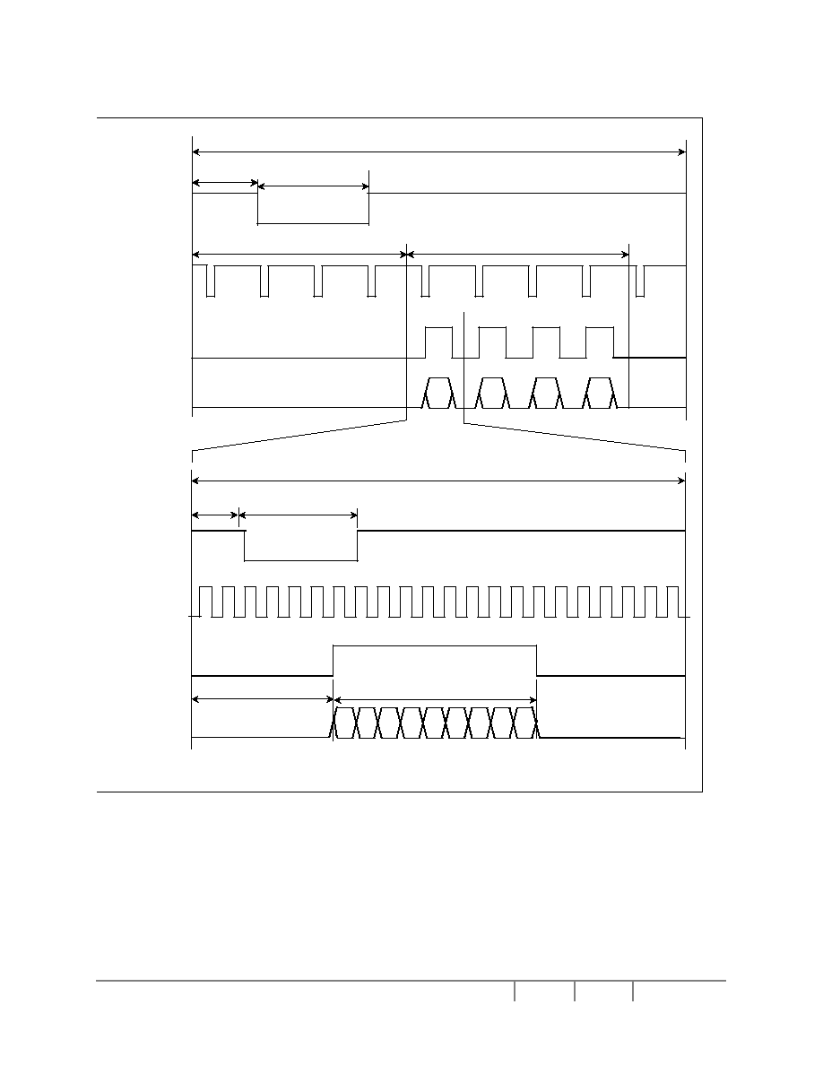
Solomon Systech
Oct 2003 P 96/144
Rev 1.4
SSD1905
10.4.6 Generic TFT Panel Timing
LDEN
HDP
HDPS
HPS
HT (= 1 Line)
VT (= 1 Frame)
VPW
VPS
VDPS
VDP
HPW
LFRAME
LLINE
LDEN
LDATA[17:0]
LLINE
LDATA[17:0]
LSHIFT
Figure 10-22 :
Generic TFT Panel Timing
VT
= Vertical Total
= [(REG[19h] bits 1-0, REG[18h] bits 7-0) + 1] lines
VPS = LFRAME Pulse Start Position
= [(REG[27h] bits 1-0, REG[26h] bits 7-0)] x HT + (REG[31h] bits 1-0, REG[30h] bits 7-0) pixels
VPW = LFRAME Pulse Width
= [(REG[24h]bits2-0)+ 1] x HT + (REG[35h] bits 1-0, REG[34h] bits 7-0) � (REG[31h] bits 1-0, REG[30h]
bits 7-0) pixels

SSD1905
Rev 1.4
P 97/144 Oct 2003
Solomon Systech
VDPS = Vertical Display Period Start Position
= [(REG[1Fh]bits1-0,REG[1Eh]bits7-0)] lines
VDP = Vertical Display Period
= [(REG[1Dh]bits1-0,REG[1Ch]bits7-0)+ 1] lines
* The VDP must be a minimum of 2 lines
HT
= Horizontal Total
= [((REG[12h] bits 6-0) + 1) x 8] pixels
HPS = LLINE Pulse Start Position
= [(REG[23h] bits 1-0, REG[22h] bits 7-0) + 1] pixels
HPW = LLINE Pulse Width
= [(REG[20h] bits 6-0)+ 1] pixels
HDPS = Horizontal Display Period Start Position
= [(REG[17h] bits 1-0, REG[16h] bits 7-0) + 5] pixels
HDP = Horizontal Display Period
= [((REG[14h] bits 6-0) + 1) x 8] pixels
The HDP must be a minimum of 32 pixels and can be increased by multiples of 8.
*Panel Type Bits (REG[10h] bits 1-0) = 01 (TFT)
*LLINE Pulse Polarity Bit (REG[24h] bit 7) = 0 (active low)
*LFRAME Polarity Bit (REG[20h] bit 7) = 0 (active low)
10.4.7 9/12/18-Bit TFT Panel Timing
HNDP
1
LDATA[11:0]
1-1
LINE480
1-640
LFRAME
LINE1
LLINE
LINE480
LDEN
LLINE
LSHIFT
LDEN
LDATA[11:0]
HDP
HNDP
2
VNDP
2
VDP
VNDP
1
Note: LDEN is used to indicated the first pixel
Example Timing for 12-bit 640x480 panel
1-2
Figure 10-23 :
12-Bit TFT Panel Timing

Solomon Systech
Oct 2003 P 98/144
Rev 1.4
SSD1905
VDP = Vertical Display Period
= VDP Lines
VNDP = Vertical Non-Display Period
= VNDP1 + VNDP2
= VT � VDP Lines
VNDP1 = Vertical Non-Display Period 1
= VNDP - VNDP2 Lines
VNDP2 = Vertical Non-Display Period 2
= VDPS - VPS Lines
if negative add VT
HDP = Horizontal Display Period
= HDP Ts
HNDP = Horizontal Non-Display Period
= HNDP1 + HNDP2
= HT - HDP Ts
HNDP1 = Horizontal Non-Display Period 1
= HDPS � HPS Ts
if negative add HT
HNDP2 = Horizontal Non-Display Period 2
= HPS - HDP + HDPS Ts
if negative add HT
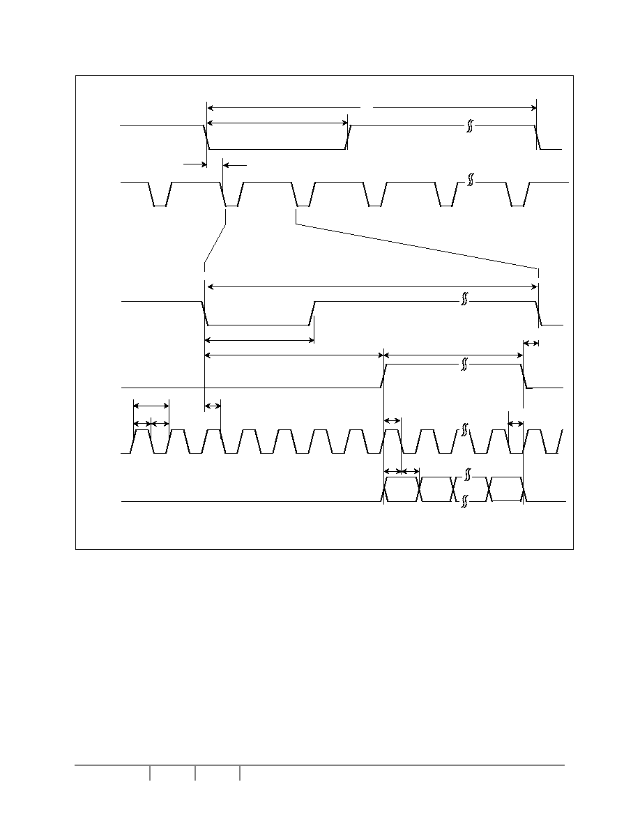
SSD1905
Rev 1.4
P 99/144 Oct 2003
Solomon Systech
t
6
t
10
t
5
LSHIFT
LFRAME
LLINE
LLINE
LDEN
LDATA[11:0]
t
9
t
11
t
10
t
12
t
1
t
2
t
3
t
4
t
8
t
16
t
15
t
13
t
14
2
639
640
1
t
7
Figure 10-24 :
TFT A.C. Timing
Solomon Systech
Oct 2003 P 100/144 Rev 1.4
SSD1905
Table 10-19 : TFT A.C. Timing
Symbol
Parameter
Min
Typ
Max
Units
t
1
LFRAME cycle time
VT
Lines
t
2
LFRAME pulse width low
VPW
Lines
t
3
LFRAME falling edge to LLINE falling edge phase
difference
HPS + 1
Ts(note1)
t
4
LLINE cycle time
HT
Ts
t
5
LLINE pulse width low
HPW
Ts
t
6
LLINE falling edge to LDEN active
note 2
250
Ts
t
7
LDEN pulse width
HDP
Ts
t
8
LDEN falling edge to LLINE falling edge
note 3
Ts
t
9
LSHIFT period
1
Ts
t
10
LSHIFT pulse width high
0.5
Ts
t
11
LSHIFT pulse width low
0.5
Ts
t
12
LLINE setup to LSHIFT falling edge
0.5
Ts
t
13
LDEN to LSHIFT falling edge setup time
0.5
Ts
t
14
LDEN hold from LSHIFT falling edge
0.5
Ts
t
15
Data setup to LSHIFT falling edge
0.5
Ts
t
16
Data hold from LSHIFT falling edge
0.5
Ts
1. Ts = pixel clock period
2. t
6
min = HDPS - HPS
if negative add HT
3. t
8
min = HPS - (HDP + HDPS )
if negative add HT
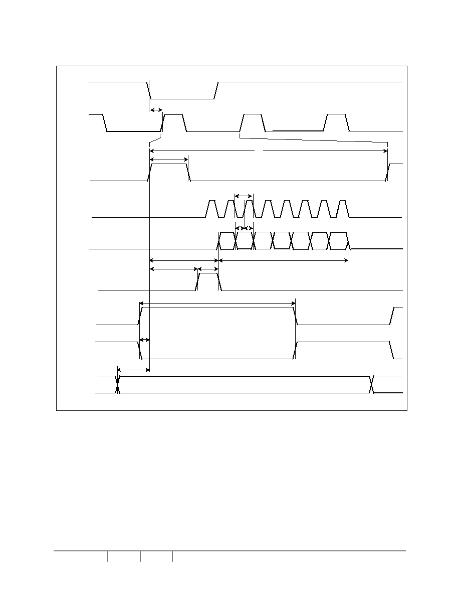
SSD1905
Rev 1.4
P 101/144 Oct 2003
Solomon Systech
10.4.8 160x160 Sharp HR-TFT Panel Timing (e.g. LQ031B1DDxx)
t
5
t
10
t
6
t
9
t
7
t
12
LDATA[17:0]
D160
t
3
GPIO3
(SPL)
LFRAME
(SPS)
LLINE
(LP)
LSHIFT
(CLK)
GPIO1
(CLS)
t
13
t
1
t
2
t
4
t
8
D1
D2
D3
LLINE
(LP)
GPIO0
(PS)
GPIO2
(REV)
t
11
Figure 10-25 :
160x160 Sharp HR-TFT Panel Horizontal Timing
Solomon Systech
Oct 2003 P 102/144 Rev 1.4
SSD1905
Table 10-20 : 160x160 Sharp HR-TFT Horizontal Timing
Symbol Parameter
Min Typ Max Units
t
1
LLINE start position
13
Ts (note 1)
t
2
Horizontal total period
180
Ts
t
3
LLINE width
2
Ts
t
4
LSHIFT period
1
Ts
t
5
Data setup to LSHIFT rising edge
0.5
Ts
t
6
Data hold from LSHIFT rising edge
0.5
Ts
t
7
Horizontal display start position
5
Ts
t
8
Horizontal display period
160
Ts
t
9
LLINE rising edge to GPIO3 rising edge
4
Ts
t
10
GPIO3 pulse width
1
Ts
t
11
GPIO1(GPIO0) pulse width
136
Ts
t
12
GPIO1 rising edge (GPIO0 falling edge) to LLINE rise edge
4
Ts
t
13
GPIO2 toggle edge to LLINE rise edge
10
Ts
1. Ts = pixel clock period
2. t
1
typ = (REG[22h] bits 7-0) + 1
3. t
2
typ = ((REG[12h] bits 6-0) + 1) x 8
4. t
3
typ = (REG[20h] bits 6-0) + 1
5. t
7
typ = ((REG[16h] bits 7-0) + 1) - ((REG[22h] bits 7-0) + 1)
6. t
8
typ = ((REG[14h] bits 6-0) + 1) x 8

SSD1905
Rev 1.4
P 103/144 Oct 2003
Solomon Systech
t
4
t
12
t
3
t
2
LINE1
LINE160
t
10
LLINE
(LP)
LSHIFT
(CLK)
LDATA[17:0]
LFRAME
(SPS)
GPIO1(CLS)
REG[38h]
bit 0 = 0
t
9
t
11
GPIO0(PS)
REG[38h]
bit 1 = 1
LINE2
t
1
t
14
t
13
t
6
t
7
t
8
GPIO1(CLS)
REG[38h]
bit 0 = 0
GPIO0(PS)
REG[38h]
bit 1 = 0
GPIO1(CLS)
REG[38h]
bit 0 = 1
GPIO0(PS)
REG[38h]
bit 1 = 1
t
5
Figure 10-26 :
160x160 Sharp HR-TFT Panel Vertical Timing
Solomon Systech
Oct 2003 P 104/144 Rev 1.4
SSD1905
Table 10-21 : 160x160 Sharp HR-TFT Panel Vertical Timing
Symbol Parameter
Min Typ Max Units
t
1
Vertical total period
203
Lines
t
2
Vertical display start position
40
Lines
t
3
Vertical display period
160
Lines
t
4
LFRAME sync pulse width
2
Lines
t
5
1
LFRAME falling edge to GPIO1 alternate timing start
5
Lines
t
6
1
GPIO1 alternate timing period
4
Lines
t
7
2
LFRAME falling edge to GPIO0 alternate timing start
40
Lines
t
8
2
GPIO0 alternate timing period
162
Lines
t
9
GPIO1 first pulse rising edge to LLINE rising edge
4
Ts (note 1)
t
10
1
GPIO1 first pulse width
48
Ts
t
11
1
GPIO1 first pulse falling edge to second pulse rising edge
40
Ts
t
12
1
GPIO1 second pulse width
48
Ts
t
13
2
GPIO0 falling edge to LLINE rising edge
4
Ts
t
14
2
GPIO0 low pulse width
24
Ts
1.
Ts = pixel clock period
1
Timing for CLS signal change bit enabled (REG[38h] bit 0 = 0) only
2
Timing for PS signal change bit enabled (REG[38h] bit 1 = 1) only
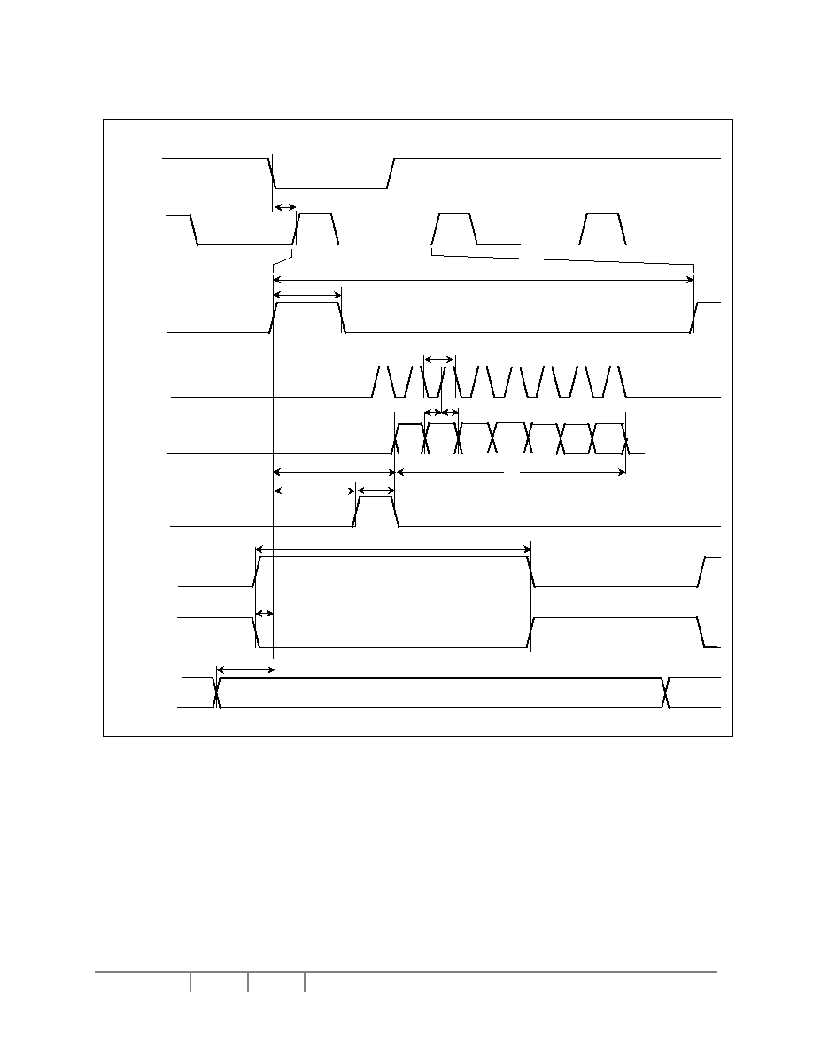
SSD1905
Rev 1.4
P 105/144 Oct 2003
Solomon Systech
10.4.9 320x240 Sharp HR-TFT Panel Timing (e.g. LQ039Q2DS01)
t
11
t
10
t
9
t
6
t
12
LDATA[17:0]
D320
t
3
t
5
GPIO3
(SPL)
LFRAME
(SPS)
LLINE
(LP)
LSHIFT
(CLK)
GPIO1
(CLS)
t
13
t
1
t
2
t
4
t
8
D1
D2
D3
LLINE
(LP)
GPIO0
(PS)
GPIO2
(REV)
t
7
Figure 10-27 :
320x240 Sharp HR-TFT Panel Horizontal Timing
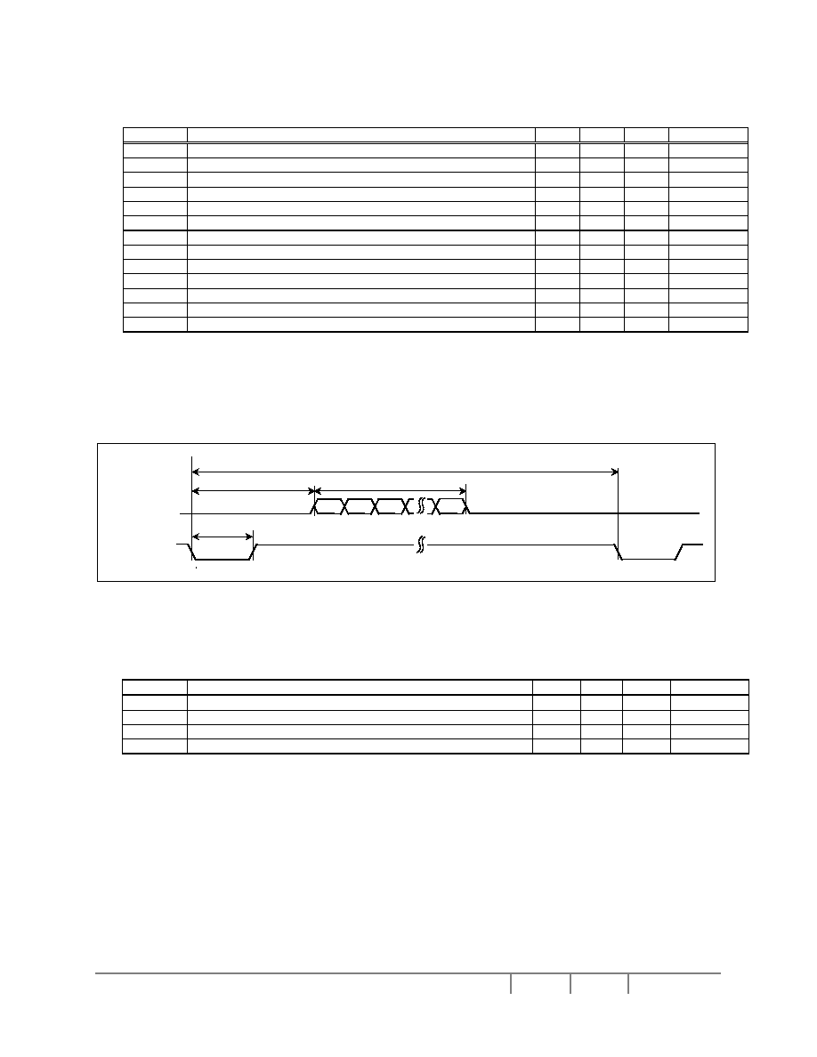
Solomon Systech
Oct 2003 P 106/144 Rev 1.4
SSD1905
Table 10-22 : 320x240 Sharp HR-TFT Panel Horizontal Timing
Symbol Parameter
Min Typ Max Units
t
1
LLINE start position
14
Ts (note 1)
t
2
Horizontal total period
400
440
Ts
t
3
LLINE width
1
Ts
t
4
LSHIFT period
1
Ts
t
5
Data setup to LSHIFT rising edge
0.5
Ts
t
6
Data hold from LSHIFT rising edge
0.5
Ts
t
7
Horizontal display start position
60
Ts
t
8
Horizontal display period
320
Ts
t
9
LLINE rising edge to GPIO3 rising edge
59
Ts
t
10
GPIO3 pulse width
1
Ts
t
11
GPIO1(GPIO0) pulse width
353
Ts
t
12
GPIO1 rising edge (GPIO0 falling edge) to LLINE rise edge
5
Ts
t
13
GPIO2 toggle edge to LLINE rise edge
11
Ts
1. Ts = pixel clock period
2. t
1
typ = (REG[22h] bits 7-0) + 1
3. t
2
typ = ((REG[12h] bits 6-0) + 1) x 8
4. t
3
typ = (REG[20h] bits 6-0) + 1
5. t
7
typ = ((REG[16h] bits 7-0) + 1) - ((REG[22h] bits 7-0) + 1)
6. t
8
typ = ((REG[14h] bits 6-0) + 1) x 8
t
4
t
3
t
2
LINE1
LINE240
LDATA[17:0]
LFRAME
(SPS)
LINE2
t
1
Figure 10-28 :
320x240 Sharp HR-TFT Panel Vertical Timing
Table 10-23 : 320x240 Sharp HR-TFT Panel Vertical Timing
Symbol Parameter
Min Typ Max Units
t
1
Vertical total period
245
330
Lines
t
2
Vertical display start position
4
Lines
t
3
Vertical display period
240
Lines
t
4
Vertical sync pulse width
2
Lines
SSD1905
Rev 1.4
P 107/144 Oct 2003
Solomon Systech
11 Clocks
The following diagram provides a block diagram of the SSD1905 internal clocks.
CLKI
MCLK
PCLK1
PWMCLK1
CLK MUX
CLKI-GEN
BCLK
MCLK
PWMCLK2
PCLK2
PCLK
PWMCLK
STOP CONTROL
CLKI
AUXCLK
STOP CONTROL
AUXCLK-GEN
Figure 11-1 :
Clock Generator Block Diagram
11.1 Clock Descriptions
11.1.1 BCLK
BCLK is an internal clock derived from CLKI. BCLK can be a divided version (
� 1, � 2, � 3, � 4) of CLKI. CLKI is
typically derived from the host CPU bus clock.
The source clock options for BCLK may be selected as in the following table.
Table 11-1 : BCLK Clock Selection
Source Clock Options
BCLK Selection
CLKI
CF[7:6] = 00
CLKI
� 2
CF[7:6] = 01
CLKI
� 3
CF[7:6] = 10
CLKI
� 4
CF[7:6] = 11
Solomon Systech
Oct 2003 P 108/144 Rev 1.4
SSD1905
Note
For synchronous bus interfaces, it is recommended that BCLK be set the same as the CPU bus clock (not a
divided version of CLKI) e.g. SH-3, SH-4.
11.1.2 MCLK
MCLK provides the internal clock required to access the embedded SRAM. The SSD1905 is designed with
efficient power saving control for clocks (clocks are turned off when not used).
Furthermore, reducing the MCLK frequency relative to the BCLK frequency increases the CPU cycle latency and
so reduces screen update performance. For a balance of power saving and performance, the MCLK should be
configured to have a high enough frequency setting to provide sufficient screen refresh as well as acceptable CPU
cycle latency.
The source clock options for MCLK may be selected as in the following table.
Table 11-2 : MCLK Clock Selection
Source Clock Options
MCLK Selection (REG[04h] bits 5:4)
BCLK
00
BCLK
� 2
01
BCLK
� 3
10
BCLK
� 4
11
11.1.3 PCLK
PCLK is the internal clock used to control the LCD panel. PCLK should be chosen to match the optimum frame
rate of the LCD panel. See Section 13 "Frame Rate Calculation" for details on the relationship between PCLK and
frame rate.
Some flexibility is possible in the selection of PCLK. Firstly, LCD panels typically have a range of permissible frame
rates. Secondly, it may be possible to choose a higher PCLK frequency and tailor the horizontal and vertical non-
display periods to lower the frame-rate to its optimal value.
The source clock options for PCLK may be selected as in the following table.
Table 11-3 : PCLK Clock Selection
Source Clock Options
PCLK Selection (REG[05h] bits 6:4)
MCLK 00h
MCLK
� 2
10h
MCLK
� 3
20h
MCLK
� 4
30h
MCLK
� 8
40h
BCLK 01h
BCLK
� 2
11h
BCLK
� 3
21h
BCLK
� 4
31h
BCLK
� 8
41h
CLKI 02h
CLKI
� 2
12h
CLKI
� 3
22h
CLKI
� 4
32h
CLKI
� 8
42h
AUXCLK 03h
AUXCLK
� 2
13h
AUXCLK
� 3
23h
AUXCLK
� 4
33h
SSD1905
Rev 1.4
P 109/144 Oct 2003
Solomon Systech
AUXCLK
� 8
43h
There is a relationship between the frequency of MCLK and PCLK that must be maintained, see Table 11-4 :
Relationship between MCLK and PCLK.
Table 11-4 : Relationship between MCLK and PCLK
Color Depth (bpp)
MCLK to PCLK Relationship
16
f
MCLK
f
PCLK
x 2
8 f
MCLK
f
PCLK
4
f
MCLK
f
PCLK
� 2
2
f
MCLK
f
PCLK
� 4
1
f
MCLK
f
PCLK
� 8
11.1.4 PWMCLK
PWMCLK is the internal clock used by the Pulse Width Modulator for output to the panel.
The source clock options for PWMCLK may be selected as in the following table.
For further information on controlling PWMCLK, see Section 7.2.9 "Pulse Width Modulation (PWM) Clock and
Contrast Voltage (CV) Pulse Configuration Registers".
Note
The SSD1905 provides Pulse Width Modulation output on the pin LPWMOUT.
LPWMOUT can be used to control LCD panels which support PWM control of the back-light inverter.
Table 11-5 :
PWMCLK Clock Selection
Source Clock Options
PWMCLK Selection REG[B1h] bit 0
CLKI
0
AUXCLK 1
11.2 Clocks versus Functions
Table 11-6 : SSD1905 Internal Clock Requirements, lists the internal clocks required for the following SSD1905
functions.
Table 11-6 : SSD1905 Internal Clock Requirements
Function
Bus Clock
(BCLK)
Memory Clock
(MCLK)
Pixel Clock
(PCLK)
PWM Clock
(PWMCLK)
Register Read/Write
Required
Not Required
Not Required
Not Required
Memory Read/Write
Required
Required
Not Required
Not Required
Look-Up Table Register
Read/Write
Required
Not Required
Not Required
Not Required
Software Power Saving Required
Not Required
Not Required
Not Required
LCD Output
Required
Required
Required
Not Required
PWM / CV Output
Required
Required
Required
Required
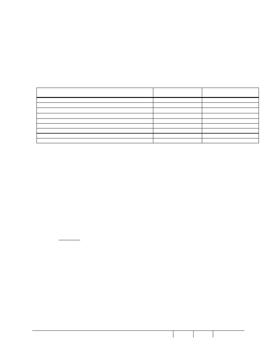
Solomon Systech
Oct 2003 P 110/144 Rev 1.4
SSD1905
12 Power Saving Mode
Power Saving Mode is incorporated into the SSD1905 to accommodate the need for power reduction in the hand-
held device market. This mode is enabled via the Power Saving Mode Enable bit (REG[A0h] bit 0).
Power Saving Mode power down the panel and stop display refresh accesses to the display buffer.
Table 12-1 : Power Saving Mode Function Summary
Software
Power
Saving
Normal
IO Access Possible?
Yes
Yes
Memory Access Possible?
No
1
Yes
Look-Up Table Registers Access Possible?
Yes
Yes
Sequence Controller Running?
No
Yes
Display Active?
No
Yes
LCD Interface Outputs
Forced Low
4
Active
PWMCLK Stopped
Active
GPIO3:0 Pins configured for HR-TFT
2
Forced Low
Active
GPIO Pins configured as GPIOs Access Possible ?
2
Yes
3
Yes
Note :
1
When Power Saving mode is enabled, the memory controlled is powered down. The status of the memory
controlled is indicated by the Memory Controller Power Saving Status bit (REG[A0h] bit 3). For Power Saving
Status AC timing, see Section 10.3.3 "Power Saving Status".
2
GPIO Pins are configured using the configurations pin CF3 which is latched on the rising edge of RESET#. For
information on CF3, see Table 5-6 : Summary of Power-On/Reset Options.
3
GPIOs can be accessed and if configured as outputs can be changed.
4
Except the LCD interface pins LDEN and LSHIFT in STN and CSTN mode.
After reset, the SSD1905 stays in Power Saving Mode. Software must initialize the chip (i.e. programs all registers)
and then clear the Power Saving Mode Enable bit.
13 Frame Rate Calculation
The following formula is used to calculate the display frame rate.
)
(
)
(
VT
x
HT
f
FrameRate
PCLK
=
Where:
f
PCLK
= PCLK frequency (Hz)
HT
= Horizontal Total
= ((REG[12h] bits 6-0) + 1) x 8 Ts
VT
= Vertical Total
= ((REG[19h] bits 1-0, REG[18h] bits 7-0) + 1) Lines
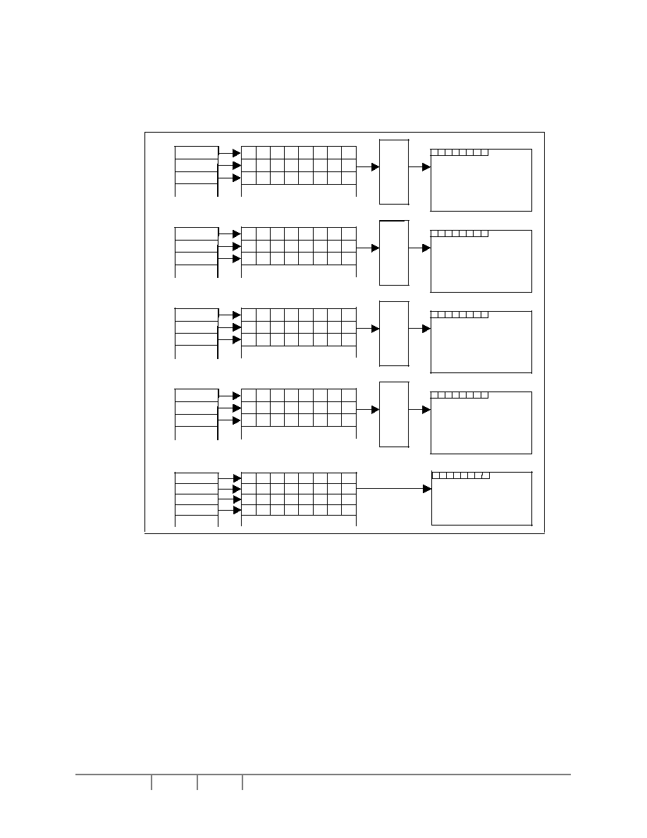
SSD1905
Rev 1.4
P 111/144 Oct 2003
Solomon Systech
14 Display Data Formats
The following diagrams show the display mode data formats.
1 bpp:
Byte 1
Byte 2
Host Address
bit 7
bit 0
A
1
A
6
A
0
A
2
A
3
A
4
A
5
A
7
A
9
A
14
A
8
A
10
A
11
A
12
A
13
A
15
A
17
A
22
A
16
A
18
A
19
A
20
A
21
A
23
LUT
P
0
P
1
P
2
P
3
P
4
P
5
P
6
P
7
P
n
= RGB value from LUT
Index (A
n
)
Panel Display
Display Buffer
2 bpp:
Byte 0
Byte 1
Byte 2
Host Address
bit 7
bit 0
B
0
A
3
A
0
A
1
B
1
A
2
B
2
B
3
B
4
A
7
A
4
A
5
B
5
A
6
B
6
B
7
B
8
A
11
A
8
A
9
B
9
A
10
B
10
B
11
LUT
P
0
P
1
P
2
P
3
P
4
P
5
P
6
P
7
P
n
= RGB value from LUT
Index (A
n
, B
n
)
Panel Display
Display Buffer
4 bpp:
Byte 0
Byte 1
Byte 2
Host Address
bit 7
bit 0
B
0
C
1
A
0
C
0
D
0
A
1
B
1
D
1
B
4
C
5
A
4
C
4
D
4
A
5
B
5
D
5
LUT
P
0
P
1
P
2
P
3
P
4
P
5
P
6
P
7
P
n
= RGB value from LUT
Index (A
n
, B
n
, C
n
, D
n
)
Panel Display
Display Buffer
8 bpp:
bit 7
bit 0
Byte 0
Byte 1
Byte 2
Host Address
B
0
G
0
A
0
C
0
D
0
E
0
F
0
H
0
B
1
G
1
A
1
C
1
D
1
E
1
F
1
H
1
B
2
G
2
A
2
C
2
D
2
E
2
F
2
H
2
LUT
P
0
P
1
P
2
P
3
P
4
P
5
P
6
P
7
P
n
= RGB value from LUT Index
(A
n
, B
n
, C
n
, D
n
, E
n
, F
n
, G
n
, H
n
)
Panel Display
Display Buffer
B
2
C
3
A
2
C
2
D
2
A
3
B
3
D
3
Byte 0
16 bpp:
P
0
P
1
P
2
P
3
P
4
P
5
P
6
P
7
Panel Display
G
0
1
B
0
1
G
0
0
B
0
4
B
0
3
B
0
2
B
0
0
G
1
1
B
1
1
G
1
0
B
1
4
B
1
3
B
1
2
B
1
0
R
0
3
G
0
4
R
0
2
R
0
1
R
0
0
G
0
5
G
0
3
R
1
3
G
1
4
R
1
2
R
1
1
R
1
0
G
1
5
G
1
3
G
0
2
R
0
4
G
1
2
R
1
4
Bypasses LUT
Byte 0
Byte 1
Byte 2
Byte 3
Host Address
Display Buffer
P
n
= (R
n
4-0
, G
n
5-0
, B
n
4-0
)
bit 7
bit 0
Figure 14-1 : 1/2/4/8/16 Bit-Per-Pixel Display Data Memory Organization
Note
1. For 16 bpp format, Rn, Gn, Bn represent the red, green, and blue color components.
Solomon Systech
Oct 2003 P 112/144 Rev 1.4
SSD1905
15 Look-Up Table Architecture
The following figures are intended to show the display data output path only.
Note
When Color Invert is enabled the display color is inverted after the Look-Up Table.
15.1 Monochrome Modes
The green Look-Up Table (LUT) is used for all monochrome modes.
15.1.1 1 Bit-per-pixel Monochrome Mode
1 bit-per-pixel data
from Display Buffer
6-bit Gray Data
Green Look-Up Table 256x6
00
01
Figure 15-1 :
1 Bit-per-pixel Monochrome Mode Data Output Path
15.1.2 2 Bit-per-pixel Monochrome Mode
2 bit-per-pixel data
from Display Buffer
6-bit Gray Data
Green Look-Up Table 256x6
00
01
02
03
Figure 15-2 :
2 Bit-per-pixel Monochrome Mode Data Output Path
SSD1905
Rev 1.4
P 113/144 Oct 2003
Solomon Systech
15.1.3 4 Bit-per-pixel Monochrome Mode
4 bit-per-pixel data
from Display Buffer
6-bit Gray Data
Green Look-Up Table 256x6
00
01
02
03
04
05
06
07
08
09
0A
0B
0C
0D
0E
0F
Figure 15-3 :
4 Bit-per-pixel Monochrome Mode Data Output Path
15.1.4 8 Bit-per-pixel Monochrome Mode
8 bit-per-pixel data
from Display Buffer
00
01
02
03
04
05
06
07
F8
F9
FA
FB
FC
FD
FE
FF
6-bit Gray Data
Green Look-Up Table 256x6
Figure 15-4 :
8 Bit-per-pixel Monochrome Mode Data Output Path
15.1.5 16 Bit-Per-Pixel Monochrome Mode
The LUT is bypassed and the green data is directly mapped for this color depth� See
Figure 14-1 : 1/2/4/8/16 Bit-Per-Pixel Display Data Memory Organization.
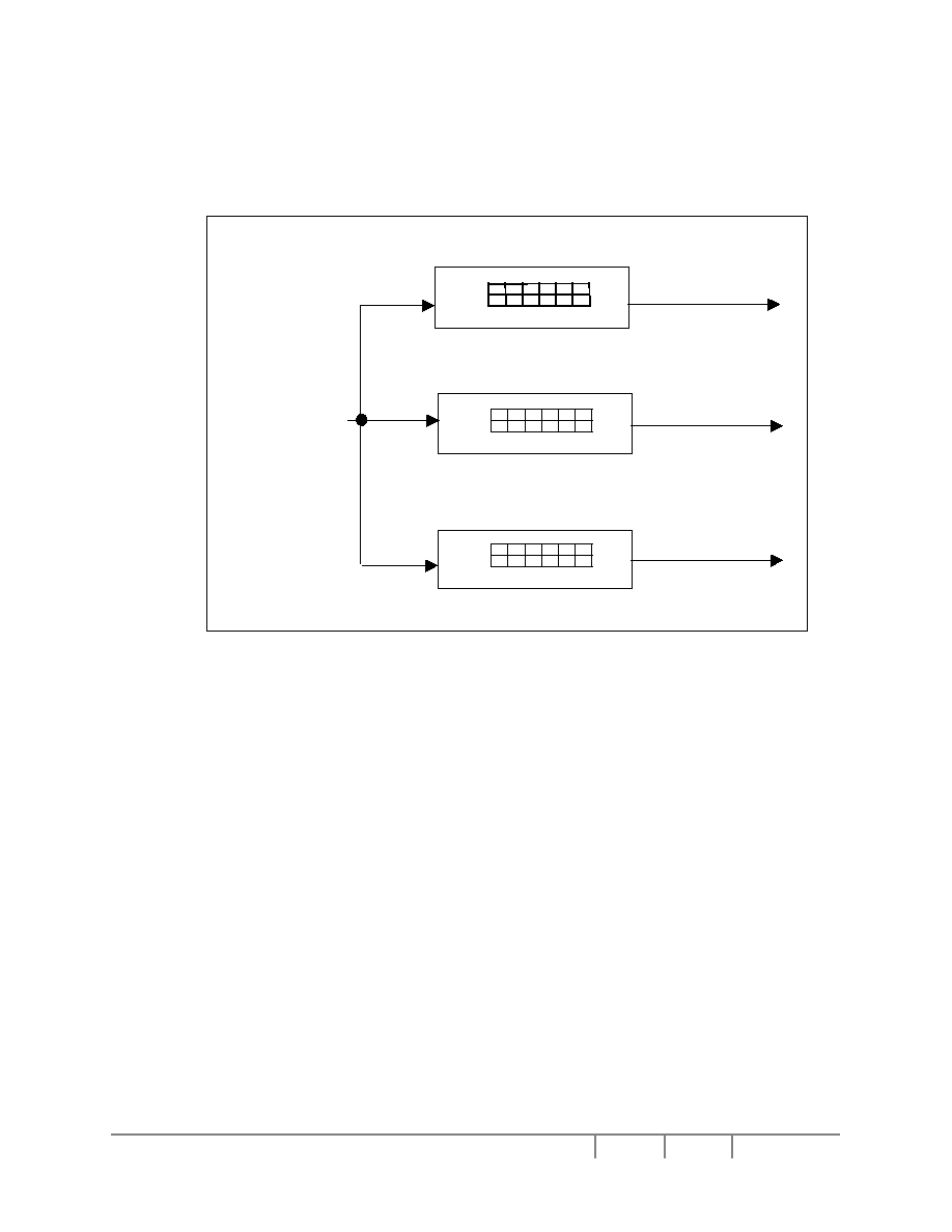
Solomon Systech
Oct 2003 P 114/144 Rev 1.4
SSD1905
15.2 Color Modes
15.2.1 1 Bit-Per-Pixel Color
1 bit-per-pixel data
from Display Buffer
00
01
6-bit Red Data
Red Look-Up Table 256x6
6-bit Green Data
Green Look-Up Table 256x6
6-bit Blue Data
Blue Look-Up Table 256x6
00
01
00
01
Figure 15-5 :
1 Bit-Per-Pixel Color Mode Data Output Path
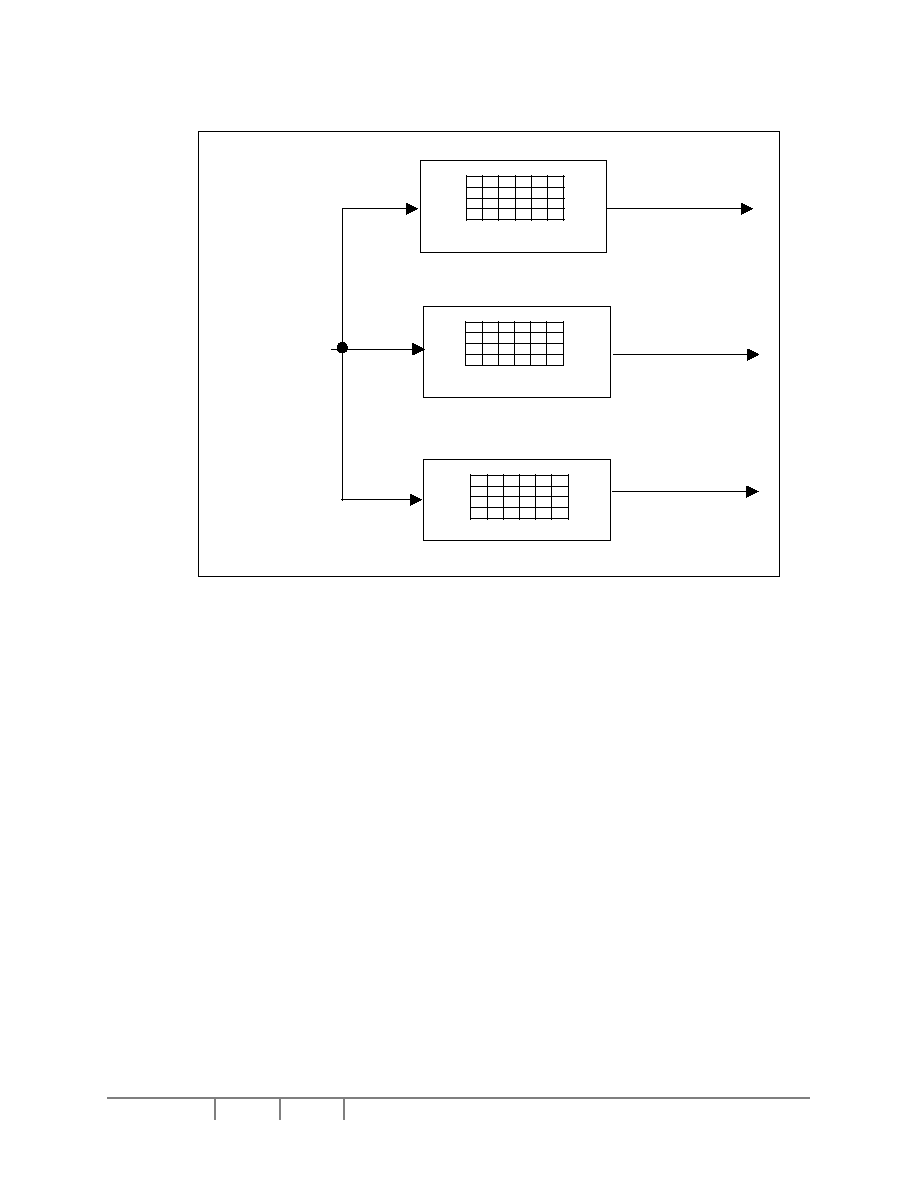
SSD1905
Rev 1.4
P 115/144 Oct 2003
Solomon Systech
15.2.2 2 Bit-Per-Pixel Color
2 bit-per-pixel data
from Display Buffer
00
01
02
03
6-bit Red Data
Red Look-Up Table 256x6
6-bit Green Data
Green Look-Up Table 256x6
6-bit Blue Data
Blue Look-Up Table 256x6
00
01
02
03
00
01
02
03
Figure 15-6 :
2 Bit-Per-Pixel Color Mode Data Output Path
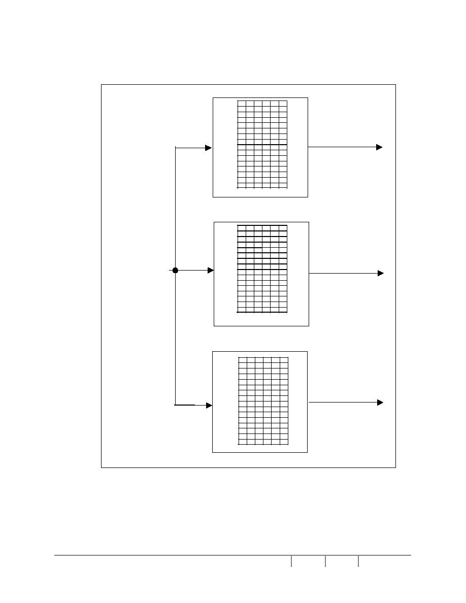
Solomon Systech
Oct 2003 P 116/144 Rev 1.4
SSD1905
15.2.3 4 Bit-Per-Pixel Color
4 bit-per-pixel data
from Display Buffer
00
01
02
03
04
05
06
07
08
09
0A
0B
0C
0D
0E
0F
6-bit Red Data
Red Look-Up Table 256x6
6-bit Green Data
Green Look-Up Table 256x6
6-bit Blue Data
Blue Look-Up Table 256x6
00
01
02
03
04
05
06
07
08
09
0A
0B
0C
0D
0E
0F
00
01
02
03
04
05
06
07
08
09
0A
0B
0C
0D
0E
0F
Figure 15-7 :
4 Bit-Per-Pixel Color Mode Data Output Path
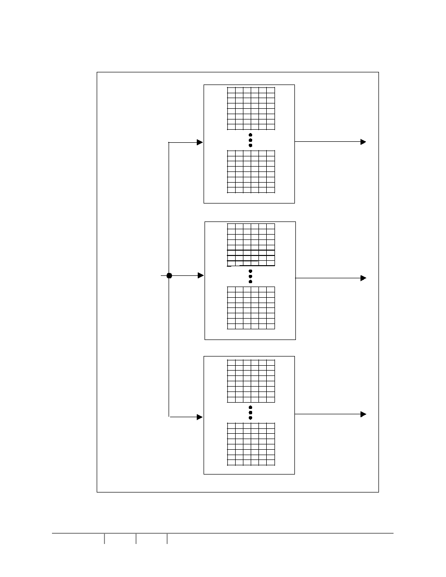
SSD1905
Rev 1.4
P 117/144 Oct 2003
Solomon Systech
15.2.4 8 Bit-per-pixel Color Mode
8 bit-per-pixel data
from Display Buffer
00
01
02
03
04
05
06
07
F8
F9
FA
FB
FC
FD
FE
FF
6-bit Red Data
Red Look-Up Table 256x6
00
01
02
03
04
05
06
07
F8
F9
FA
FB
FC
FD
FE
FF
6-bit Green Data
Green Look-Up Table 256x6
00
01
02
03
04
05
06
07
F8
F9
FA
FB
FC
FD
FE
FF
6-bit Blue Data
Blue Look-Up Table 256x6
Figure 15-8 :
8 Bit-per-pixel Color Mode Data Output Path
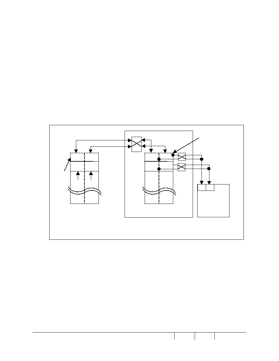
Solomon Systech
Oct 2003 P 118/144 Rev 1.4
SSD1905
15.2.5 16 Bit-Per-Pixel Color Mode
The LUT is bypassed at 16 bpp and the color data is directly mapped for this color depth. The color pixel is
arranged as 5-6-5 RGB format. See Figure 14-1 : 1/2/4/8/16 Bit-Per-Pixel Display Data Memory Organization.
16 Big-Endian Bus Interface
16.1 Byte Swapping Bus Data
The display buffer and register architecture of the SSD1905 is inherently little-endian. If configured as big-
endian (CF4 = 1 at reset), bus accesses are automatically handled by byte swapping all read/write data
to/from the internal display buffer and registers.
Bus data byte swapping translates all byte accesses correctly to the SSD1905 register and display buffer
locations. To maintain the correct translation for 16-bit word access, even address bytes must be mapped
to the MSB of the 16-bit word, and odd address bytes to the LSB of the 16-bit word. For example:
aa
cc
dd
bb
bb
dd
cc
aa
aabb ccdd
MSB
LSB
2
0
2
0
0
15
0
15
Display
Data
Byte Swap
System
Memory
Address
Display
Buffer
Address
D[15:8]
D[7:0]
* MSB is assumed to be associated with even address.
* LSB is assumed to be associated with odd address.
Display
Buffer
(Little-Endian)
System
Memory
(Big-Endian)
CPU Data
Byte Swap
Byte write 11h to register address 1Eh ->
REG[1Eh] <= 11h
Byte write 22h to register address 1Fh ->
REG[1Fh] <= 22h
Word write 1122h to register address 1Eh->
REG[1Eh] <= 11h
REG[1Fh] <= 22h
Figure 16-1 :
Byte-swapping for 16 Bpp
SSD1905
Rev 1.4
P 119/144 Oct 2003
Solomon Systech
16.1.1 16 Bpp Color Depth
For 16 bpp color depth, the Display Data Byte Swap bit (REG[71h] bit 6) must be set to 1
For 16 bpp color depth, the MSB of the 16-bit pixel data is stored at the even system memory address
location and the LSB of the 16-bit pixel data is stored at the odd system memory address location. Bus
data byte swapping (automatic when the SSD1905 is configured for Big-Endian) causes the 16-bit pixel
data to be stored byte-swapped in the SSD1905 display buffer. During display refresh this stored data
must be byte-swapped again before it is sent to the display.
16.1.2 1/2/4/8 Bpp Color Depth
For 1/2/4/8 bpp color depth, byte swapping must be performed on the bus data but not the display data.
For 1/2/4/8 bpp color depth, the Display Data Byte Swap bit (REG[71h] bit 6) must be set to 0.
11
22
22
11
11
22
0
0
0
15
0
15
System
Memory
Address
Display
Buffer
Address
D[15:8]
D[7:0]
* High byte lane (D[15:8]) data (e.g. 11) is associated with even address.
* Low byte lane (D[7:0]) data (e.g. 22) is associated with odd address.
Display
Buffer
(Little-Endian)
System
Memory
(Big-Endian)
CPU Data
Byte Swap
Figure 16-2 :
Byte-swapping for 1/2/4/8 Bpp

Solomon Systech
Oct 2003 P 120/144 Rev 1.4
SSD1905
17 Virtual Display Mode
Virtual display refers to the situation where the image to be viewed is larger than the physical display. The
difference can be in the horizontal, vertical or both dimensions. To view the image, the display is used as a
window into the display buffer. At any given time only a portion of the image is visible. Panning and scrolling
are used to view the full image. Panning describes the horizontal (side to side) motion of the display area.
Scrolling describes the vertical (up and down) motion of the display area.
The Main Window Display Start Address register specifies the starting address of main window image in the
display buffer. The Main Window Line Address Offset register determines the number of horizontal pixels in
the virtual image. Figure 17-1 : Main Window inside Virtual Image Area illustrates the situation.
320 x 240
Virtual Image Area
240 x 160
Main Window
Panning
Scrolling
Figure 17-1 : Main Window inside Virtual Image Area

SSD1905
Rev 1.4
P 121/144 Oct 2003
Solomon Systech
18 Display Rotate Mode
Most computer displays are refreshed in landscape orientation � from left to right and top to bottom. Computer
images are stored in the same manner. Display Rotate Mode is designed to rotate the displayed image on an
LCD by 90
�, 180�, or 270� in an counter-clockwise direction. The rotation is done in hardware and is
transparent to the user for all display buffer reads and writes. By processing the rotation in hardware, Display
Rotate Mode offers a performance advantage over software rotation of the displayed image.
The image is not actually rotated in the display buffer since there is no address translation during CPU
read/write. The image is rotated during display refresh.
18.1 90� Display Rotate Mode
The following figure shows how the programmer sees a 160x240 rotated image and how the image is being
displayed. The application image is written to the SSD1905 in the following sense: A�B�C�D. The display is
refreshed by the SSD1905 in the following sense: B-D-A-C.
A B
C D
Display
Rotate
Window
160
240
A B
C D
D
i
sp
l
a
y
Rot
a
t
e
Wi
ndow
240
160
display start address
(panel origin)
physical memory
start address
image seen by programmer
= image in display buffer
image refreshed by SSD1905
Figure 18-1 : Relationship Between The Screen Image and the Image Refreshed in 90
�
�
�
� Display Rotate
Mode.
18.1.1 Register Programming
Enable 90
�
�
�
� Display Rotate Mode
Set Display Rotate Mode Select bits to 01 (REG[71h] bits 1:0 = 01).
Display Start Address
The display refresh circuitry starts at pixel "B", therefore the Main Window Display Start Address
registers (REG[74h], REG[75h], REG[76h]) must be programmed with the address of pixel "B".
To calculate the value of the address of pixel "B" use the following formula (assumes 8bpp color
depth).
Main Window Display Start Address bits 16-0
= ((Image address + (panel height x bpp
� 8)) � 4) �1
= ((0 + (160 pixels x 8 bpp
� 8)) � 4) � 1
= 39 (27h)
Solomon Systech
Oct 2003 P 122/144 Rev 1.4
SSD1905
Line Address Offset
The Main Window Line Address Offset register (REG[78h], REG[79h]) is based on the display
width and programmed using the following formula.
Main Window Line Address Offset bits 9-0
= Display width in pixels
� (32 � bpp)
= 160 pixels
� (32 � 8 bpp)
= 40 (28h)
18.2 180� Display Rotate Mode
The following figure shows how the programmer sees a 240x160 landscape image and how the image is
being displayed. The application image is written to the SSD1905 in the following sense: A�B�C�D. The
display is refreshed by the SSD1905 in the following sense: D-C-B-A.
A B
C D
Display
Rotate
Window
physical memory
start address
image seen by programmer
= image in display buffer
160
240
240
160
display start address
(panel origin)
image refreshed by SSD1905
Disp
lay
Rota
te
Window
A
B
C
D
Figure 18-2 : Relationship Between The Screen Image and the Image Refreshed in 180
�
�
�
� Display Rotate
Mode.
18.2.1 Register Programming
Enable 180
�
�
�
� Display Rotate Mode
Set Display Rotate Mode Select bits to 10 (REG[71h] bits 1:0 = 10).
Display Start Address
The display refresh circuitry starts at pixel "D", therefore the Main Window Display Start Address
registers (REG[74h], REG[75h], REG[76h]) must be programmed with the address of pixel "D".
To calculate the value of the address of pixel "D" use the following formula (assumes 8bpp color
depth).
Main Window Display Start Address bits 16-0
= ((Image address + (image width x (panel height � 1) + panel width) x bpp
� 8) � 4) �1
= ((0 + (240 pixels x 159 pixels + 240 pixels) x 8 bpp
� 8) � 4) � 1
= 9599 (257Fh)

SSD1905
Rev 1.4
P 123/144 Oct 2003
Solomon Systech
Line Address Offset
The Main Window Line Address Offset register (REG[78h], REG[79h]) is based on the display
width and programmed using the following formula.
Main Window Line Address Offset bits 9-0
= Display width in pixels
� (32 � bpp)
= 240 pixels
� (32 � 8 bpp)
= 60 (3Ch)
18.3 270� Display Rotate Mode
The following figure shows how the programmer sees a 160x240 rotated image and how the image is
being displayed. The application image is written to the SSD1905 in the following sense: A�B�C�D. The
display is refreshed by the SSD1905 in the following sense: C-A-D-B.
A B
C D
Display
Rotate
Window
160
240
D
C
B
A
D
i
sp
l
a
y
Rot
a
t
e
Wi
ndow
240
160
display start address
(panel origin)
physical memory
start address
image seen by programmer
= image in display buffer
image refreshed by SSD1905
Figure 18-3 : Relationship Between The Screen Image and the Image Refreshed in 270
�
�
�
� Display Rotate
Mode.
18.3.1 Register Programming
Enable 270
�
�
�
� Display Rotate Mode
Set Display Rotate Mode Select bits to 11 (REG[71h] bits 1:0 = 11).
Display Start Address
The display refresh circuitry starts at pixel "C", therefore the Main Window Display Start Address
registers (REG[74h], REG[75h], REG[76h]) must be programmed with the address of pixel "C".
To calculate the value of the address of pixel "C" use the following formula (assumes 8bpp color
depth).
Main Window Display Start Address bits 16-0
= (Image address + ((panel width � 1) x image width x bpp
� 8) � 4)
= (0 + ((240 pixels � 1) x 160 pixels x 8 bpp
� 8) � 4)
= 9560 (2558h)
Solomon Systech
Oct 2003 P 124/144 Rev 1.4
SSD1905
Line Address Offset
The Main Window Line Address Offset register (REG[78h], REG[79h]) is based on the display
width and programmed using the following formula.
Main Window Line Address Offset bits 9-0
= Display width in pixels
� (32 � bpp)
= 160 pixels
� (32 � 8 bpp)
= 40 (28h)
19 Floating Window Mode
This mode enables a floating window within the main display window. The floating window can be
positioned anywhere within the virtual display and is controlled through the Floating Window control
registers (REG[7Ch] through REG[91h]). The floating window retains the same color depth and display
orientation as the main window.
The following diagram shows an example of a floating window within a main window and the registers
used to position it.
Normal Orientation Mode
Floating Window Start Y Position
(REG[89h],REG[88h])
Floating Window
Main Window
Floating Window End Y Position
(REG[91h],REG[90h])
Floating Window End X Position
(REG[8Dh],REG[8Ch])
panel's origin
Floating Window Start X Position
(REG[85h],REG[84h])
Figure 19-1 :
Floating Window with Display Rotate Mode disabled
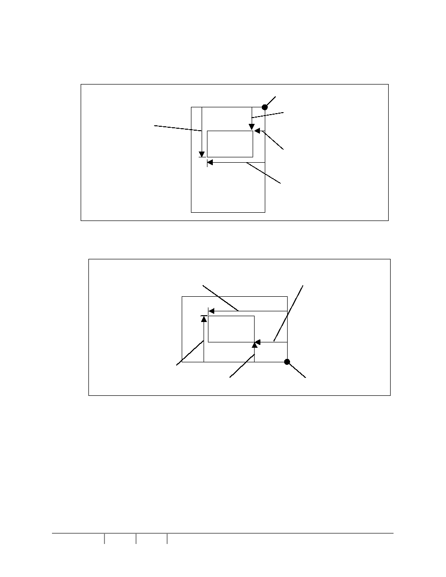
SSD1905
Rev 1.4
P 125/144 Oct 2003
Solomon Systech
19.1 With Display Rotate Mode Enabled
19.1.1 Display Rotate Mode 90�
90
�
�
�
� Display Rotate Mode
Floating Window Start Y Position
(REG[89h],REG[88h])
Floating window
Main Window
Floating Window End Y Position
(REG[91h],REG[90h])
Floating Window Start X Position
(REG[85h],REG[84h])
Floating Window End X Position
(REG[8Dh],REG[8Ch])
panel's origin
Figure 19-2 :
Floating Window with Display Rotate Mode 90� enabled
19.1.2 Display Rotate Mode 180�
180
�
�
�
� Display Rotate Mode
Floating Window
Main Window
Floating Window Start X Position
(REG[85h],REG[84h])
Floating Window End X Position
(REG[8Dh],REG[8Ch])
panel's origin
Floating Window Start Y Position
(REG[89h],REG[88h])
Floating Window End Y Position
(REG[91h],REG[90h])
Figure 19-3 :
Floating Window with Display Rotate Mode 180� enabled
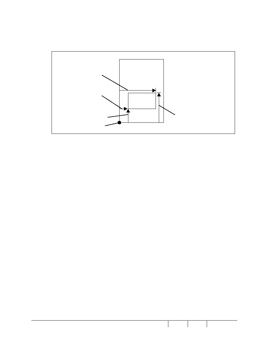
Solomon Systech
Oct 2003 P 126/144 Rev 1.4
SSD1905
19.1.3 Display Rotate Mode 270�
270
�
�
�
� Display Rotate Mode
Floating Window Start Y Position
(REG[89h],REG[88h])
Floating Window
Main Window
Floating Window End Y Position
(REG[91h],REG[90h])
Floating Window Start X Position
(REG[85h],REG[84h])
Floating Window End X Position
(REG[8Dh],REG[8Ch])
panel's origin
Figure 19-4
: Floating Window with Display Rotate Mode 270� enabled

SSD1905
Rev 1.4
P 127/144 Oct 2003
Solomon Systech
20 Hardware Cursor Mode
This mode enables two cursors on the main display window. The cursors can be positioned anywhere within the
display and are controlled through Cursor Mode registers (REG[C0h] through REG[111h]). Cursor support is
available only at 4/8/16-bpp display modes.
Each cursor pixel is 2-bit and the indexing scheme is as follows:
Table 20-1 : Indexing scheme for Hardware Cursor
Value
Color of Cursor 1 / Cursor 2
00
Transparent
01
Content of color index 1 register
(REG[E1h], REG[E0h] / REG[109h], REG[108h])
10
Content of color index 2 register
(REG[E5h], REG[E4h] / REG[10Dh], REG[10Ch])
11
Content of color index 3 register
(REG[E9h], REG[E8h] / REG[111h], REG[110h])
Three 16-bit color index registers (REG[E0h] through REG[111h]) have been implemented for each cursor. Only
the lower portion of the color index register is used in 4/8-bpp display modes. The LUT is bypassed and the color
data is directly mapped for 16-bpp display mode.
4 Bit-per-pixel
15
12 11
8 7
4 3
0
Don't Care
4-bit Color Index
8 Bit-per-pixel
15
12 11
8 7
4 3
0
Don't Care
8-bit Color Index
16 Bit-per-pixel (the index registers represents the 16-bit color component)
15 13
12
8
7
3
2 0
Green Component
Bits 2-0
Blue Component
Bits 4-0
Red Component
Bits 4-0
Green Component
Bits 5-3
The display precedence is Cursor1 > Cursor2 > Floating window > Main Window.
Main Window
Floating Window
Cursor 1
Cursor 2
Figure 20-1 : Display Precedence in Hardware Cursor
Note :
The maximum size for cursor is 32x32 pixels, while the minimum size varies for different color depths and display
orientations.

Solomon Systech
Oct 2003 P 128/144 Rev 1.4
SSD1905
The cursors retains the same color depth and display orientation as the main window. The following diagram
shows an example of two cursors within a main window and the registers used to position it.
Cursor1
Main-Window
Cursor1 Position X
(REG[D1h],REG[D0h])
panel's origin
Cursor1 Position Y
(REG[D5h],REG[D4h])
Cursor2
Cursor2 Position Y
(REG[FDh],REG[FCh])
Cursor2 Position X
(REG[F9h],REG[F8h])
Figure 20-2 : Cursors on the main window
20.1 With Display Rotate Mode Enabled
20.1.1 Display Rotate Mode 90
�
�
�
�
Cursor1
Main-Window
Cursor1 Position X
(REG[D1h],REG[D0h])
panel's origin
Cursor1 Position Y
(REG[D5h],REG[D4h])
Cursor2
Cursor2 Position Y
(REG[FDh],REG[FCh])
Cursor2 Position X
(REG[F9h],REG[F8h])
Figure 20-3 : Cursors with Display Rotate Mode 90
�
�
�
�
enabled
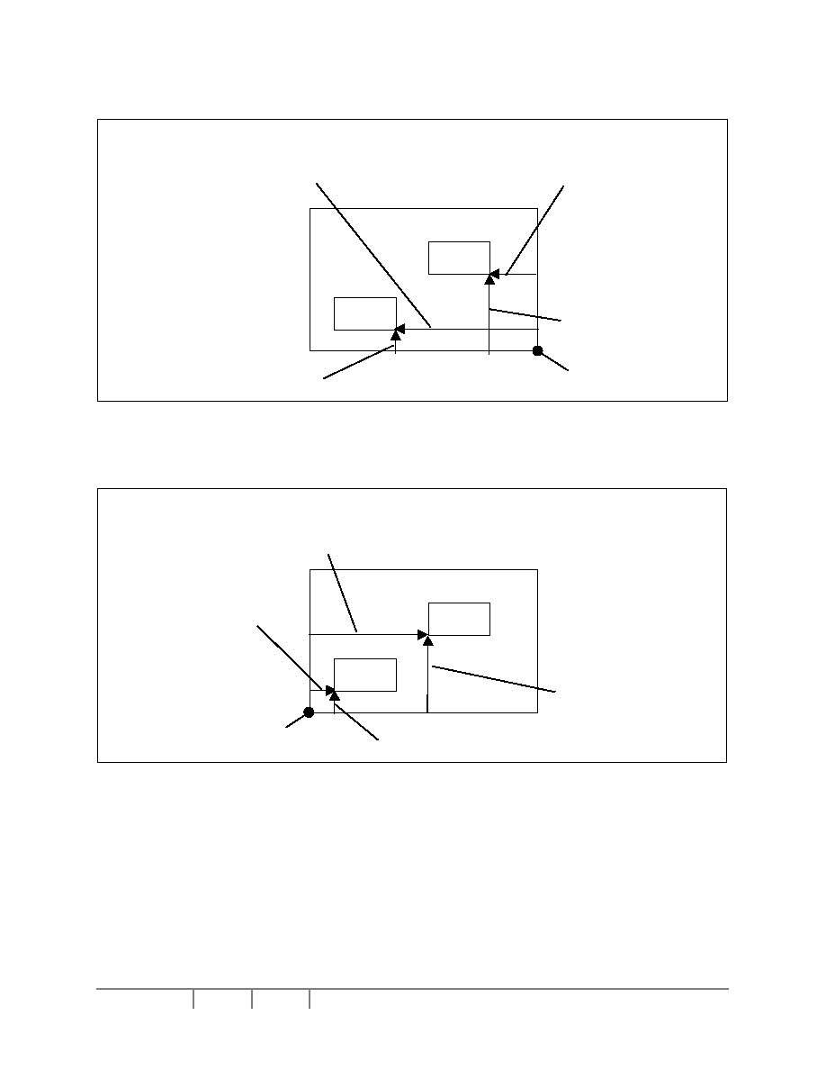
SSD1905
Rev 1.4
P 129/144 Oct 2003
Solomon Systech
20.1.2 Display Rotate Mode 180
�
�
�
�
Cursor1
Main-Window
Cursor1 Position X
(REG[D1h],REG[D0h])
panel's origin
Cursor1 Position Y
(REG[D5h],REG[D4h])
Cursor2
Cursor2 Position Y
(REG[FDh],REG[FCh])
Cursor2 Position X
(REG[F9h],REG[F8h])
Figure 20-4 : Cursors with Display Rotate Mode 180
�
�
�
�
enabled
20.1.3 Display Rotate Mode 270
�
�
�
�
Cursor1
Main-Window
Cursor1 Position X
(REG[D1h],REG[D0h])
panel's origin
Cursor1 Position Y
(REG[D5h],REG[D4h])
Cursor2
Cursor2 Position Y
(REG[FDh],REG[FCh])
Cursor2 Position X
(REG[F9h],REG[F8h])
Figure 20-5 : Cursors with Display Rotate Mode 270
�
�
�
�
enabled
20.2 Pixel format (Normal orientation mode)
Assume the pixel data stores start at address n, which n must be divisible by 4 (i.e. aligned to 32-bit boundary).
In this example, a 16x16 cursor is displayed which each cursor index is defined by x and y coordinate, C(y,x).
Solomon Systech
Oct 2003 P 130/144 Rev 1.4
SSD1905
20.2.1 4/8/16 Bit-per-pixel
7 6 5 4 3 2 1 0
Addr. n
C(0,0)
C(0,1)
C(0,2)
C(0,3)
Addr. n + 1
C(0,4)
C(0,5)
C(0,6)
C(0,7)
Addr. n + 2
C(0,8)
C(0,9)
C(0,10)
C(0,11)
Addr. n + 3
C(0,12)
C(0,13)
C(0,14)
C(0,15)
Addr. n + 4
C(1,0)
C(1,1)
C(1,2)
C(1,3)
.
.
.
Addr. n + 60
C(15,0)
C(15,1)
C(15,2)
C(15,3)
Addr. n + 61
C(15,4)
C(15,5)
C(15,6)
C(15,7)
Addr. n + 62
C(15,8)
C(15,9)
C(15,10)
C(15,11)
Addr. n + 63
C(15,12)
C(15,13)
C(15,14)
C(15,15)
20.3 Pixel format (90� Display Rotate Mode)
Assume the pixel data stores start at address n, which n must be divisible by 4 (i.e. aligned to 32-bit boundary).
In this example, a 16x16 cursor is displayed which each cursor index is defined x and y coordinate, C(y,x).
20.3.1 4 Bit-per-pixel
7 6 5 4 3 2 1 0
Addr. n
C(0,8)
C(0,9)
C(0,10)
C(0,11)
Addr. n + 1
C(0,12)
C(0,13)
C(0,14)
C(0,15)
Addr. n + 2
C(1,8)
C(1,9)
C(1,10)
C(1,11)
Addr. n + 3
C(1,12)
C(1,13)
C(1,14)
C(1,15)
.
.
.
Addr. n + 28
C(14,8)
C(14,9)
C(14,10)
C(14,11)
Addr. n + 29
C(14,12)
C(14,13)
C(14,14)
C(14,15)
Addr. n + 30
C(15,8)
C(15,9)
C(15,10)
C(15,11)
Addr. n + 31
C(15,12)
C(15,13)
C(15,14)
C(15,15)
Addr. n + 32
C(0,0)
C(0,1)
C(0,2)
C(0,3)
Addr. n + 33
C(0,4)
C(0,5)
C(0,6)
C(0,7)
Addr. n + 34
C(1,0)
C(1,1)
C(1,2)
C(1,3)
Addr. n + 35
C(1,4)
C(1,5)
C(1,6)
C(1,7)
.
.
.
Addr. n + 60
C(14,0)
C(14,1)
C(14,2)
C(14,3)
Addr. n + 61
C(14,4)
C(14,5)
C(14,6)
C(14,7)
Addr. n + 62
C(15,0)
C(15,1)
C(15,2)
C(15,3)
Addr. n + 63
C(15,4)
C(15,5)
C(15,6)
C(15,7)
SSD1905
Rev 1.4
P 131/144 Oct 2003
Solomon Systech
20.3.2 8 Bit-per-pixel
7 6 5 4 3 2 1 0
Addr. n
C(0,12)
C(0,13)
C(0,14)
C(0,15)
Addr. n + 1
C(1,12)
C(1,13)
C(1,14)
C(1,15)
Addr. n + 2
C(2,12)
C(2,13)
C(2,14)
C(2,15)
Addr. n + 3
C(3,12)
C(3,13)
C(3,14)
C(3,15)
.
.
.
Addr. n + 12
C(12,12)
C(12,13)
C(12,14)
C(12,15)
Addr. n + 13
C(13,12)
C(13,13)
C(13,14)
C(13,15)
Addr. n + 14
C(14,12)
C(14,13)
C(14,14)
C(14,15)
Addr. n + 15
C(15,12)
C(15,13)
C(15,14)
C(15,15)
Addr. n + 16
C(0,8)
C(0,9)
C(0,10)
C(0,11)
Addr. n + 17
C(1,8)
C(1,9)
C(1,10)
C(1,11)
Addr. n + 18
C(2,8)
C(2,9)
C(2,10)
C(2,11)
Addr. n + 19
C(3,8)
C(3,9)
C(3,10)
C(3,11)
.
.
.
Addr. n + 60
C(12,0)
C(12,1)
C(12,2)
C(12,3)
Addr. n + 61
C(13,0)
C(13,1)
C(13,2)
C(13,3)
Addr. n + 62
C(14,0)
C(14,1)
C(14,2)
C(14,3)
Addr. n + 63
C(15,0)
C(15,1)
C(15,2)
C(15,3)
20.3.3 16 Bit-per-pixel
7 6 5 4 3 2 1 0
Addr. n
C(0,14)
C(0,15)
C(1,14)
C(1,15)
Addr. n + 1
C(2,14)
C(2,15)
C(3,14)
C(3,15)
Addr. n + 2
C(4,14)
C(4,15)
C(5,14)
C(5,15)
Addr. n + 3
C(6,14)
C(6,15)
C(7,14)
C(7,15)
Addr. n + 4
C(8,14)
C(8,15)
C(9,14)
C(9,15)
Addr. n + 5
C(10,14)
C(10,15)
C(11,14)
C(11,15)
Addr. n + 6
C(12,14)
C(12,15)
C(12,14)
C(12,15)
Addr. n + 7
C(14,14)
C(14,15)
C(15,14)
C(15,15)
Addr. n + 8
C(0,12)
C(0,13)
C(1,12)
C(1,13)
Addr. n + 9
C(2,12)
C(2,13)
C(3,12)
C(3,13)
Addr. n + 10
C(4,12)
C(4,13)
C(5,12)
C(5,13)
Addr. n + 11
C(6,12)
C(6,13)
C(7,12)
C(7,13)
.
.
.
Addr. n + 60
C(8,0)
C(8,1)
C(9,0)
C(9,1)
Addr. n + 61
C(10,0)
C(10,1)
C(11,0)
C(11,1)
Addr. n + 62
C(12,0)
C(12,1)
C(12,0)
C(12,1)
Addr. n + 63
C(14,0)
C(14,1)
C(15,0)
C(15,1)
Solomon Systech
Oct 2003 P 132/144 Rev 1.4
SSD1905
20.4 Pixel format (180� Display Rotate Mode)
Assume the pixel data stores start at address n, which n must be divisible by 4 (i.e. aligned to 32-bit boundary).
In this example, a 16x16 cursor is displayed which each cursor index is defined by x and y coordinate, C(y,x).
20.4.1 4 Bit-per-pixel
7 6 5 4 3 2 1 0
Addr. n
C(15,8)
C(15,9)
C(15,10)
C(15,11)
Addr. n + 1
C(15,12)
C(15,13)
C(15,14)
C(15,15)
Addr. n + 2
C(15,0)
C(15,1)
C(15,2)
C(15,3)
Addr. n + 3
C(15,4)
C(15,5)
C(15,6)
C(15,7)
Addr. n + 4
C(14,8)
C(14,9)
C(14,10)
C(14,11)
.
.
.
Addr. n + 60
C(0,8)
C(0,9)
C(0,10)
C(0,11)
Addr. n + 61
C(0,12)
C(0,13)
C(0,14)
C(0,15)
Addr. n + 62
C(0,0)
C(0,1)
C(0,2)
C(0,3)
Addr. n + 63
C(0,4)
C(0,5)
C(0,6)
C(0,7)
20.4.2 8 Bit-per-pixel
7 6 5 4 3 2 1 0
Addr. n
C(15,12)
C(15,13)
C(15,14)
C(15,15)
Addr. n + 1
C(15,8)
C(15,9)
C(15,10)
C(15,11)
Addr. n + 2
C(15,4)
C(15,5)
C(15,6)
C(15,7)
Addr. n + 3
C(15,0)
C(15,1)
C(15,2)
C(15,3)
Addr. n + 4
C(14,12)
C(14,13)
C(14,14)
C(14,15)
.
.
.
Addr. n + 60
C(0,12)
C(0,13)
C(0,14)
C(0,15)
Addr. n + 61
C(0,8)
C(0,9)
C(0,10)
C(0,11)
Addr. n + 62
C(0,4)
C(0,5)
C(0,6)
C(0,7)
Addr. n + 63
C(0,0)
C(0,1)
C(0,2)
C(0,3)

SSD1905
Rev 1.4
P 133/144 Oct 2003
Solomon Systech
20.4.3 16 Bit-per-pixel
7 6 5 4 3 2 1 0
Addr. n
C(15,14)
C(15,15)
C(15,12)
C(15,13)
Addr. n + 1
C(15,10)
C(15,11)
C(15,8)
C(15,9)
Addr. n + 2
C(15,6)
C(15,7)
C(15,4)
C(15,5)
Addr. n + 3
C(15,2)
C(15,3)
C(15,0)
C(15,1)
Addr. n + 4
C(14,14)
C(14,15)
C(14,12)
C(14,13)
.
.
.
Addr. n + 60
C(0,14)
C(0,15)
C(0,12)
C(0,13)
Addr. n + 61
C(0,10)
C(0,11)
C(0,8)
C(0,9)
Addr. n + 62
C(0,6)
C(0,7)
C(0,4)
C(0,5)
Addr. n + 63
C(0,2)
C(0,3)
C(0,0)
C(0,1)
20.5 Pixel format (270� Display Rotate Mode)
Assume the pixel data stores start at address n, which n must be divisible by 4 (i.e. aligned to 32-bit boundary).
In this example, a 16x16 cursor is displayed which each cursor index is defined by x and y coordinate, C(y,x).
20.5.1 4 Bit-per-pixel
7 6 5 4 3 2 1 0
Addr. n
C(15,0)
C(15,1)
C(15,2)
C(15,3)
Addr. n + 1
C(15,4)
C(15,5)
C(15,6)
C(15,7)
Addr. n + 2
C(14,0)
C(14,1)
C(14,2)
C(14,3)
Addr. n + 3
C(14,4)
C(14,5)
C(14,6)
C(14,7)
.
.
.
Addr. n + 28
C(1,0)
C(1,1)
C(1,2)
C(1,3)
Addr. n + 29
C(1,4)
C(1,5)
C(1,6)
C(1,7)
Addr. n + 30
C(0,0)
C(0,1)
C(0,2)
C(0,3)
Addr. n + 31
C(0,4)
C(0,5)
C(0,6)
C(0,7)
Addr. n + 32
C(15,8)
C(15,9)
C(15,10)
C(15,11)
Addr. n + 33
C(15,12)
C(15,13)
C(15,14)
C(15,15)
Addr. n + 34
C(14,8)
C(14,9)
C(14,10)
C(14,11)
Addr. n + 35
C(14,12)
C(14,13)
C(14,14)
C(14,15)
.
.
.
Addr. n + 60
C(1,8)
C(1,9)
C(1,10)
C(1,11)
Addr. n + 61
C(1,12)
C(1,13)
C(1,14)
C(1,15)
Addr. n + 62
C(0,8)
C(0,9)
C(0,10)
C(0,11)
Addr. n + 63
C(0,12)
C(0,13)
C(0,14)
C(0,15)
Solomon Systech
Oct 2003 P 134/144 Rev 1.4
SSD1905
20.5.2 8 Bit-per-pixel
7 6 5 4 3 2 1 0
Addr. n
C(15,0)
C(15,1)
C(15,2)
C(15,3)
Addr. n + 1
C(14,0)
C(14,1)
C(14,2)
C(14,3)
Addr. n + 2
C(13,0)
C(13,1)
C(13,2)
C(13,3)
Addr. n + 3
C(12,0)
C(12,1)
C(12,2)
C(12,3)
.
.
.
Addr. n + 12
C(3,0)
C(3,1)
C(3,2)
C(3,3)
Addr. n + 13
C(2,0)
C(2,1)
C(2,2)
C(2,3)
Addr. n + 14
C(1,0)
C(1,1)
C(1,2)
C(1,3)
Addr. n + 15
C(0,0)
C(0,1)
C(0,2)
C(0,3)
Addr. n + 16
C(15,4)
C(15,5)
C(15,6)
C(15,7)
Addr. n + 17
C(14,4)
C(14,5)
C(14,6)
C(14,7)
Addr. n + 18
C(13,4)
C(13,5)
C(13,6)
C(13,7)
Addr. n + 19
C(12,4)
C(12,5)
C(12,6)
C(12,7)
.
.
.
Addr. n + 60
C(3,12)
C(3,13)
C(3,14)
C(3,15)
Addr. n + 61
C(2,12)
C(2,13)
C(2,14)
C(2,15)
Addr. n + 62
C(1,12)
C(1,13)
C(1,14)
C(1,15)
Addr. n + 63
C(0,12)
C(0,13)
C(0,14)
C(0,15)
20.5.3 16 Bit-per-pixel
7 6 5 4 3 2 1 0
Addr. n
C(15,0)
C(15,1)
C(14,0)
C(14,1)
Addr. n + 1
C(13,0)
C(13,1)
C(12,0)
C(12,1)
Addr. n + 2
C(11,0)
C(11,1)
C(10,0)
C(10,1)
Addr. n + 3
C(9,0)
C(9,1)
C(8,0)
C(8,1)
Addr. n + 4
C(7,0)
C(7,1)
C(6,0)
C(6,1)
Addr. n + 5
C(5,0)
C(5,1)
C(4,0)
C(4,1)
Addr. n + 6
C(3,0)
C(3,1)
C(2,0)
C(2,1)
Addr. n + 7
C(1,0)
C(1,1)
C(0,0)
C(0,1)
Addr. n + 8
C(15,2)
C(15,3)
C(14,2)
C(14,3)
Addr. n + 9
C(13,2)
C(13,3)
C(12,2)
C(12,3)
Addr. n + 10
C(11,2)
C(11,3)
C(10,2)
C(10,3)
Addr. n + 11
C(9,2)
C(9,3)
C(8,2)
C(8,3)
.
.
.
Addr. n + 60
C(7,14)
C(7,15)
C(6,14)
C(6,15)
Addr. n + 61
C(5,14)
C(5,15)
C(4,14)
C(4,15)
Addr. n + 62
C(3,14)
C(3,15)
C(2,14)
C(2,15)
Addr. n + 63
C(1,14)
C(1,15)
C(0,14)
C(0,15)

SSD1905
Rev 1.4
P 135/144 Oct 2003
Solomon Systech
21 APPLICATION EXAMPLES
AU
XC
L
K
CF
0
CF
1
CF
0
CF
2
Bia
s
Po
w
e
r
8-Bit
CSTN
LCD
Display
D[7:0]
LFRAME
LLINE
LSHIFT
MOD
COREVDD
IOVDD
LDATA[7:0]
LFRAME
LLINE
LSHIFT
LDEN
GPO
BS#
M/R#
CS#
A[16:1]
D[15:0]
WE0#
WE1#
RD0#
RD/WR#
WAIT#
CLKI
RESET#
A0
Generic #1
BUS
A[27:17]
CSn#
A[16:1]
D[15:0]
WE0#
WE1#
RD0#
RD1#
WAIT#
BUSCLK
RESET#
Oscillator
Decoder
SSD1905
3.3V
0.1�F
0.1�F
0.1�F
IOVDD
10k
4.7k
0.1�F
IOVDD
4.7k
10k
10k
Figure 21-1: Typical System Diagram (Generic #1 Bus)
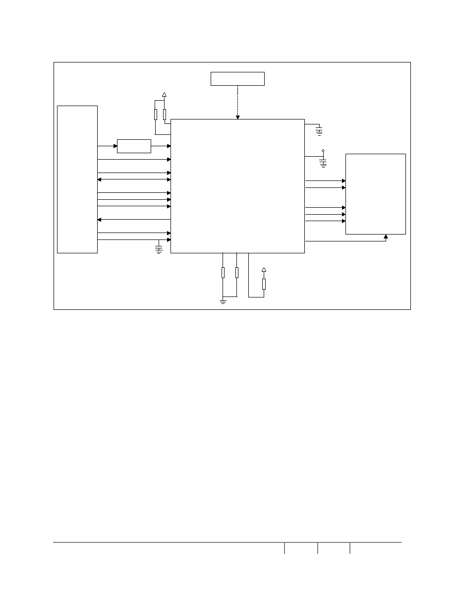
Solomon Systech
Oct 2003 P 136/144 Rev 1.4
SSD1905
AU
XC
L
K
CF
0
CF
1
CF
0
CF
2
Bia
s
Po
w
e
r
9-Bit
TFT
Display
D[8:0]
LFRAME
LLINE
LSHIFT
LDEN
COREVDD
IOVDD
LDATA[8:0]
LFRAME
LLINE
LSHIFT
LDEN
GPO
BS#
RD/WR#
M/R#
CS#
A[16:0]
D[15:0]
WE0#
WE1#
RD#
WAIT#
CLKI
RESET#
Generic #2
BUS
A[27:17]
CSn#
A[16:0]
D[15:0]
WE#
BHE#
RD#
WAIT#
BUSCLK
RESET#
Oscillator
Decoder
SSD1905
3.3V
0.1�F
0.1�F
0.1�F
IOVDD
10k
10k
0.1�F
IOVDD
10k
4.7k
4.7k
Figure 21-2 : Typical System Diagram (Generic #2 Bus)

SSD1905
Rev 1.4
P 137/144 Oct 2003
Solomon Systech
AU
XC
L
K
CF
0
CF
1
CF
0
CF
2
Bia
s
Po
w
e
r
18-Bit
HR-TFT
Display
D[17:0]
SPS
LP
CLK
PS
CLS
REV
SPL
COREVDD
IOVDD
LDATA[17:0]
LFRAME
LLINE
LSHIFT
GPIO0
GPIO1
GPIO2
GPIO3
GPO
RD#
WE0#
M/R#
CS#
A[16:1]
D[15:0]
A0
WE1#
BS#
RD/WR#
WAIT#
CLKI
RESET#
MC68K #1
BUS
A[23:17],
FC0, FC1
A[16:1]
D[15:0]
LDS#
UDS#
AS#
R/W#
DTACK#
CLK
RESET#
Oscillator
3.3V
SSD1905
Decoder
Decoder
0.1�F
0.1�F
IOVDD
10k
10k
0.1�F
IOVDD
10k
4.7k
4.7k
Figure 21-3 : Typical System Diagram (MC68K # 1, Motorola 16-Bit 68000)
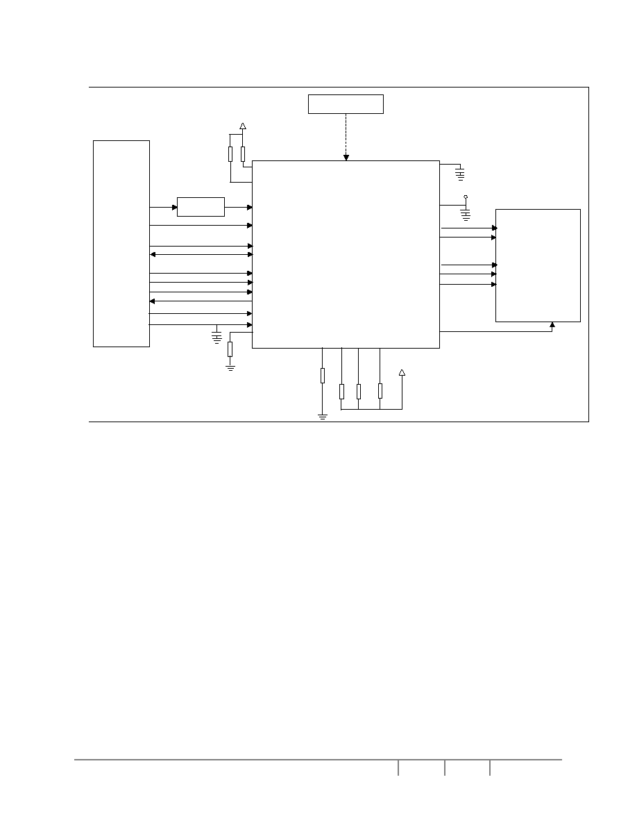
Solomon Systech
Oct 2003 P 138/144 Rev 1.4
SSD1905
AU
XC
L
K
CF
0
CF
1
CF
0
CF
2
CF
5
Bia
s
Po
w
e
r
12-bit
TFT
Display
D[11:0]
LSHIFT
LFRAME
LLINE
LDEN
COREVDD
IOVDD
LDATA[11:0]
LSHIFT
LFRAME
LLINE
LDEN
GPO
BS#
RD/WR#
M/R#
CS#
A[16:1]
D[15:0]
WE0#
WE1#
RD #
WAIT#
CLKI
RESET#
A0
MC68EZ328/
MC68VZ328
DragonBall
BUS
A[25:17]
CSX#
A[16:1]
D[15:0]
LWE#
UWE#
OE#
DTACK#
CLKO
RESET#
Oscillator
SSD1905
Decoder
3.3V
0.1
�F
0.1
�F
0.1
�F
IOVDD
10k
10k
4.7k
0.1
�F
IOVDD
10k
4.7k
10k
10k
Figure 21-4 : Typical System Diagram (Motorola MC68EZ328/MC68VZ328 "DragonBall" Bus)
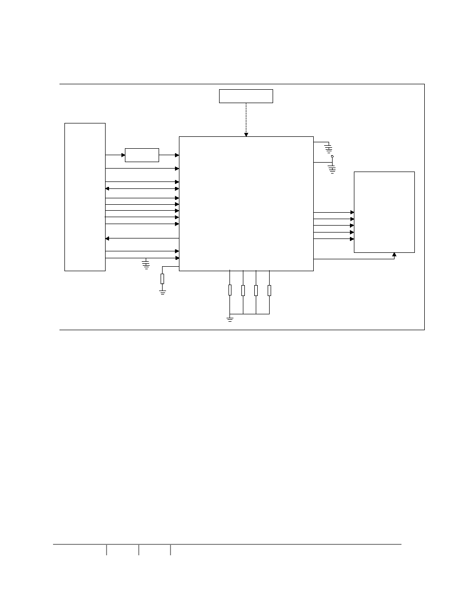
SSD1905
Rev 1.4
P 139/144 Oct 2003
Solomon Systech
AU
X
C
L
K
CF
0
CF
1
CF
0
CF
2
CF
5
B
i
as
P
o
wer
12-Bit
TFT
Display
D[11:0]
LFRAME
LLINE
LSHIFT
LDEN
COREVDD
IOVDD
LDATA[11:0]
LFRAME
LLINE
LSHIFT
LDEN
GPO
M/R#
CS#
A[16:1]
D[15:0]
WE0#
WE1#
BS#
RD/WR#
RD#
WAIT#
CLKI
RESET#
A0
SH-3
BUS
A[25:17]
CSn#
A[16:1]
D[15:0]
WE0#
WE1#
BS#
RD/WR#
RD#
WAIT#
CKIO
RESET#
Oscillator
Decoder
3.3V
SSD1905
4.7k
4.7k
4.7k
4.7k
4.7k
Figure 21-5 : Typical System Diagram (Hitachi SH-3 Bus)
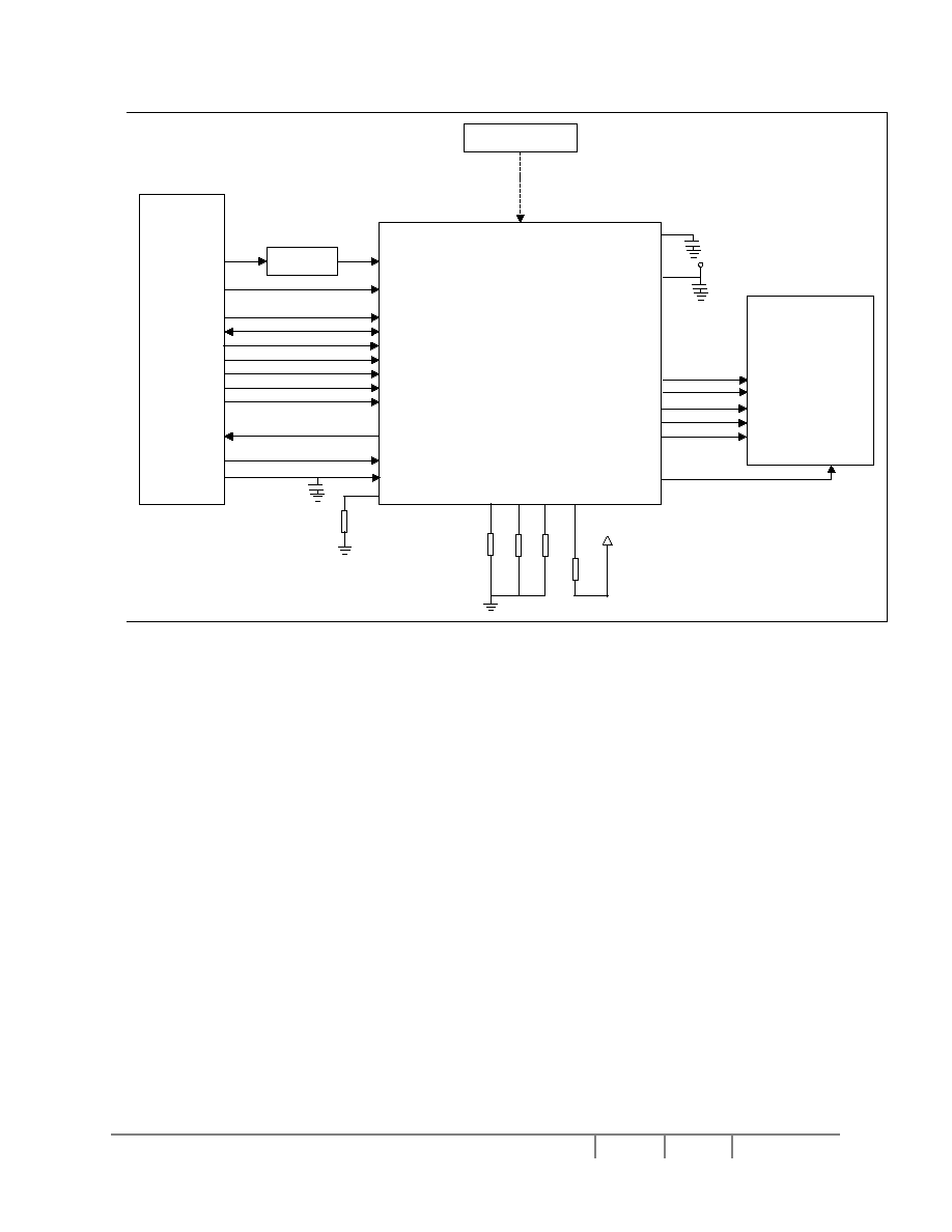
Solomon Systech
Oct 2003 P 140/144 Rev 1.4
SSD1905
AU
X
C
L
K
CF
0
CF
1
CF
0
CF
2
CF
5
Bia
s
Po
we
r
18-Bit
TFT
Display
D[17:0]
LFRAME
LLINE
LSHIFT
LDEN
COREVDD
IOVDD
LDATA[17:0]
LFRAME
LLINE
LSHIFT
LDEN
GPO
M/R#
CS#
A[16:1]
D[15:0]
WE0#
WE1#
BS#
RD/WR#
RD#
WAIT#
CLKI
RESET#
A0
SH-4
BUS
A[25:17]
CSn#
A[16:1]
D[15:0]
WE0#
WE1#
BS#
RD/WR#
RD#
RDY#
CKIO
RESET#
Oscillator
Decoder
3.3V
SSD1905
4.7k
4.7k
4.7k
IOVDD
10k
4.7k
Figure 21-6 : Typical System Diagram (Hitachi SH-4 Bus)
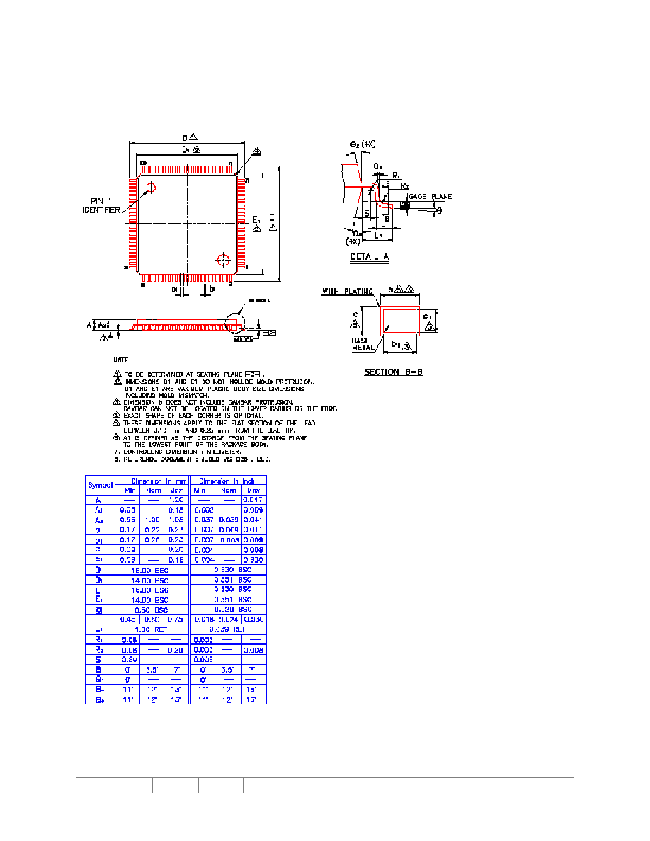
SSD1905
Rev 1.4
P 141/144 Oct 2003
Solomon Systech
22 APPENDIX
22.1 Package Mechanical Drawing for 100 pins TQFP
Solomon Systech
Oct 2003 P 142/144 Rev 1.4
SSD1905
22.2 Register Table
Table 22-1 : SSD1905 Register Table (1 of 2)
Register Pg
Register Pg
Read-Only Configuration Registers
Floating Window Registers
REG[01h] Display Buffer Size Register
15
REG[7Ch] Floating Window Display Start Address Register 0
36
REG[02h] Configuration Readback Register
15
REG[7Dh] Floating Window Display Start Address Register 1
36
REG[03h] Product / Revision Code Register
16
REG[7Eh] Floating Window Display Start Address Register 2
36
Clock Configuration Registers
REG[80h] Floating Window Line Address Offset Register 0
37
REG[04h] Memory Clock Configuration Register
16
REG[81h] Floating Window Line Address Offset Register 1
37
REG[05h] Pixel Clock Configuration Register
16
REG[84h] Floating Window Start Position X Register 0
37
Look-Up Table Registers
REG[85h] Floating Window Start Position X Register 1
38
REG[08h] Look-Up Table Blue Write Data Register
17
REG[88h] Floating Window Start Position Y Register 0
38
REG[09h] Look-Up Table Green Write Data Register
18
REG[89h] Floating Window Start Position Y Register 1
39
REG[0Ah] Look-Up Table Red Write Data Register
18
REG[8Ch] Floating Window End Position X Register 0
39
REG[0Bh] Look-Up Table Write Address Register
19
REG[8Dh] Floating Window End Position X Register 1
40
REG[0Ch] Look-Up Table Blue Read Data Register
19
REG[90h] Floating Window End Position Y Register 0
40
REG[0Dh] Look-Up Table Green Read Data Register
19
REG[91h] Floating Window End Position Y Register 1
41
REG[0Eh] Look-Up Table Red Read Data Register
20
Miscellaneous Registers
REG[0Fh] Look-Up Table Read Address Register
20
REG[A0h] Power Saving Configuration Register
41
Panel Configuration Registers
REG[A2h] Software Reset Register
42
REG[10h] Panel Type Register
21
REG[A4h] Scratch Pad Register 0
42
REG[11h] MOD Rate Register
22
REG[A5h] Scratch Pad Register 1
42
REG[12h] Horizontal Total Register
22
General Purpose IO Pins Registers
REG[14h] Horizontal Display Period Register
23
REG[A8h] General Purpose IO Pins Configuration Register 0
43
REG[16h] Horizontal Display Period Start Position Register 0
23
REG[A9h] General Purpose IO Pins Configuration Register 1
44
REG[17h] Horizontal Display Period Start Position Register 1
23
REG[ACh] General Purpose IO Pins Status/Control Register 0
44
REG[18h] Vertical Total Register 0
23
REG[ADh] General Purpose IO Pins Status/Control Register 1
45
REG[19h] Vertical Total Register 1
24
PWM Clock and CV Pulse Configuration Registers
REG[1Ch] Vertical Display Period Register 0
24
REG[B0h] PWM Clock / CV Pulse Control Register
46
REG[1Dh] Vertical Display Period Register 1
24
REG[B1h] PWM Clock / CV Pulse Configuration Register
47
REG[1Eh] Vertical Display Period Start Position Register 0
25
REG[B2h] CV Pulse Burst Length Register
48
REG[1Fh] Vertical Display Period Start Position Register 1
25
REG[B3h] PWM Duty Cycle Register
48
REG[20h] LLINE Pulse Width Register
25
REG[22h] LLINE Pulse Start Position Register 0
26
REG[23h] LLINE Pulse Start Position Register 1
26
REG[24h] LFRAME Pulse Width Register
26
REG[26h] LFRAME Pulse Start Position Register 0
27
REG[27h] LFRAME Pulse Start Position Register 1
27
REG[30h] LFRAME Pulse Start Offset Register 0
27
REG[31h] LFRAME Pulse Start Offset Register 1
27
REG[34h] LFRAME Pulse Stop Offset Register 0
28
REG[35h] LFRAME Pulse Stop Offset Register 1
28
REG[38h] HR-TFT Special Output Register
28
REG[3Ch] GPIO0 Pulse Start Register
29
REG[3Eh] GPIO0 Pulse Stop Register
29
REG[40h] GPIO2 Pulse Delay Register
30
REG[45h] STN Color Depth Control Register
30
REG[50h] Dynamic Dithering Control Register
31
Display Mode Registers
REG[70h] Display Mode Register
31
REG[71h] Special Effects Register
33
REG[74h] Main Window Display Start Address Register 0
34
REG[75h] Main Window Display Start Address Register 1
34
REG[76h] Main Window Display Start Address Register 2
35
REG[78h] Main Window Line Address Offset Register 0
35
REG[79h] Main Window Line Address Offset Register 1
35
SSD1905
Rev 1.4
P 143/144 Oct 2003
Solomon Systech
Table 22-2 : SSD1905 Register Table (2 of 2)
Register Pg
Cursor Mode Registers
REG[C0h] Cursor Feature Register
49
REG[C4h] Cursor1 Blink Total Register 0
49
REG[C5h] Cursor1 Blink Total Register 1
49
REG[C8h] Cursor1 Blink On Register 0
50
REG[C9h] Cursor1 Blink On Register 1
50
REG[CCh] Cursor1 Memory Start Register 0
50
REG[CDh] Cursor1 Memory Start Register 1
50
REG[CEh] Cursor1 Memory Start Register 2
50
REG[D0h] Cursor1 Position X Register 0
51
REG[D1h] Cursor1 Position X Register 1
51
REG[D4h] Cursor1 Position Y Register 0
51
REG[D5h] Cursor1 Position Y Register 1
51
REG[D8h] Cursor1 Horizontal size Register
52
REG[DCh] Cursor1 Vertical size Register
52
REG[E0h] Cursor1 Color Index1 Register 0
53
REG[E1h] Cursor1 Color Index1 Register 1
53
REG[E4h] Cursor1 Color Index2 Register 0
53
REG[E5h] Cursor1 Color Index2 Register 1
54
REG[E8h] Cursor1 Color Index3 Register 0
54
REG[E9h] Cursor1 Color Index3 Register 1
54
REG[ECh] Cursor2 Blink Total Register 0
54
REG[EDh] Cursor2 Blink Total Register 1
55
REG[F0h] Cursor2 Blink On Register 0
55
REG[F1h] Cursor2 Blink On Register 1
55
REG[F4h] Cursor2 Memory Start Register 0
55
REG[F5h] Cursor2 Memory Start Register 1
56
REG[F6h] Cursor2 Memory Start Register 2
56
REG[F8h] Cursor2 Position X Register 0
56
REG[F9h] Cursor2 Position X Register 1
56
REG[FCh] Cursor2 Position Y Register 0
56
REG[FDh] Cursor2 Position Y Register 1
57
REG[100h] Cursor2 Horizontal size Register
57
REG[104h] Cursor2 Vertical size Register
57
REG[108h] Cursor2 Color Index1 Register 0
58
REG[109h] Cursor2 Color Index1 Register 1
58
REG[10Ch] Cursor2 Color Index2 Register 0
58
REG[10Dh] Cursor2 Color Index2 Register 1
58
REG[110h] Cursor2 Color Index3 Register 0
59
REG[111h] Cursor2 Color Index3 Register 1
59

Solomon Systech
Oct 2003 P 144/144 Rev 1.4
SSD1905
Solomon Systech reserves the right to make changes without further notice to any products herein. Solomon Systech makes no warranty,
representation or guarantee regarding the suitability of its products for any particular purpose, nor does Solomon Systech assume any liability arising
out of the application or use of any product or circuit, and specifically disclaims any and all liability, including without limitation consequential or
incidental damages. "Typical" parameters can and do vary in different applications. All operating parameters, including "Typicals" must be validated
for each customer application by customer's technical experts. Solomon Systech does not convey any license under its patent rights nor the rights of
others. Solomon Systech products are not designed, intended, or authorized for use as components in systems intended for surgical implant into the
body, or other applications intended to support or sustain life, or for any other application in which the failure of the Solomon Systech product could
create a situation where personal injury or death may occur. Should Buyer purchase or use Solomon Systech products for any such unintended or
unauthorized application, Buyer shall indemnify and hold Solomon Systech and its offices, employees, subsidiaries, affiliates, and distributors
harmless against all claims, costs, damages, and expenses, and reasonable attorney fees arising out of, directly or indirectly, any claim of personal
injury or death associated with such unintended or unauthorized use, even if such claim alleges that Solomon Systech was negligent regarding the
design or manufacture of the part.
http://www.solomon-systech.com