
SN8P1602B
8-Bit Micro-Controller
SONiX TECHNOLOGY CO., LTD
Version 1.1
SN8P1602B
USER'S MANUAL
General Release Specification
S
S
O
O
N
N
i
i
X
X
8
8
-
-
B
B
i
i
t
t
M
M
i
i
c
c
r
r
o
o
-
-
C
C
o
o
n
n
t
t
r
r
o
o
l
l
l
l
e
e
r
r
SONIX reserves the right to make change without further notice to any products herein to improve reliability, function or design. SONIX does not
assume any liability arising out of the application or use of any product or circuit described herein; neither does it convey any license under its patent
rights nor the rights of others. SONIX products are not designed, intended, or authorized for us as components in systems intended, for surgical
implant into the body, or other applications intended to support or sustain life, or for any other application in which the failure of the SONIX product
could create a situation where personal injury or death may occur. Should Buyer purchase or use SONIX products for any such unintended or
unauthorized application. Buyer shall indemnify and hold SONIX and its officers, employees, subsidiaries, affiliates and distributors harmless against
all claims, cost, damages, and expenses, and reasonable attorney fees arising out of, directly or indirectly, any claim of personal injury or death
associated with such unintended or unauthorized use even if such claim alleges that SONIX was negligent regarding the design or manufacture of
the part.
SN8P1602B
8-Bit Micro-Controller
SONiX TECHNOLOGY CO., LTD
Version 1.1
AMENDENT HISTORY
Version Date
Description
VER 1.0
Sep. 2003
V1.0 First Issue
VER 1.1
Sep. 2003
1. Remove approval sheet
2. Remove PCB layout notice section.
3. Modify the description of code option notice.
4. Add the description of PEDGE register.
5. Modify the description of INTRQ register.
6. Change operating voltage range from "2.2V ~ 5.5V" to "2.4V ~ 5.5V" at
Fosc=3.579545 MHz, ambient temperature = 25
∞
C.

SN8P1602B
8-Bit Micro-Controller
SONiX TECHNOLOGY CO., LTD
Page 3
Version 1.1
Table of Content
AMENDENT HISTORY ............................................................................................................................... 2
1
1
1
PRODUCT OVERVIEW................................................................................................................. 8
GENERAL DESCRIPTION........................................................................................................................... 8
UPGRADE FROM SN8P1602/SN8P1603/SN8P1602A............................................................................... 8
FEATURES .................................................................................................................................................... 9
SELECTION TABLE..................................................................................................................................... 9
SYSTEM BLOCK DIAGRAM.................................................................................................................... 10
PIN ASSIGNMENT ..................................................................................................................................... 11
PIN DESCRIPTIONS .................................................................................................................................. 12
PIN CIRCUIT DIAGRAMS ........................................................................................................................ 12
2
2
2
CODE OPTION TABLE ............................................................................................................... 13
SN8P1602B .................................................................................................................................................. 13
3
3
3
ADDRESS SPACES ....................................................................................................................... 14
PROGRAM MEMORY (ROM)................................................................................................................... 14
OVERVIEW .............................................................................................................................................. 14
USER RESET VECTOR ADDRESS (0000H) ........................................................................................... 15
INTERRUPT VECTOR ADDRESS (0008H) ............................................................................................ 15
CHECKSUM CALCULATION ................................................................................................................. 17
GENERAL PURPOSE PROGRAM MEMORY AREA.............................................................................. 18
LOOK-UP TABLE DESCRIPTION.......................................................................................................... 18
JUMP TABLE DESCRIPTION................................................................................................................. 20
DATA MEMORY (RAM) ........................................................................................................................... 22
OVERVIEW .............................................................................................................................................. 22
WORKING REGISTERS............................................................................................................................. 23
Y, Z REGISTERS ...................................................................................................................................... 23

SN8P1602B
8-Bit Micro-Controller
SONiX TECHNOLOGY CO., LTD
Page 4
Version 1.1
R REGISTERS........................................................................................................................................... 24
PROGRAM FLAG ....................................................................................................................................... 25
RESET/WAKEUP FLAG .......................................................................................................................... 25
CARRY FLAG........................................................................................................................................... 25
DECIMAL CARRY FLAG......................................................................................................................... 25
ZERO FLAG ............................................................................................................................................. 25
ACCUMULATOR ....................................................................................................................................... 26
STACK OPERATIONS ............................................................................................................................... 27
OVERVIEW .............................................................................................................................................. 27
STACK REGISTERS................................................................................................................................. 28
STACK OPERATION EXAMPLE............................................................................................................. 29
PROGRAM COUNTER............................................................................................................................... 29
ONE ADDRESS SKIPPING ..................................................................................................................... 30
MULTI-ADDRESS JUMPING ................................................................................................................. 31
4
4
4
ADDRESSING MODE................................................................................................................... 32
OVERVIEW................................................................................................................................................. 32
IMMEDIATE ADDRESSING MODE....................................................................................................... 32
DIRECTLY ADDRESSING MODE .......................................................................................................... 32
INDIRECTLY ADDRESSING MODE ...................................................................................................... 32
5
5
5
SYSTEM REGISTER .................................................................................................................... 33
OVERVIEW................................................................................................................................................. 33
SYSTEM REGISTER ARRANGEMENT (BANK 0)................................................................................. 33
BYTES of SYSTEM REGISTER ................................................................................................................ 33
BITS of SYSTEM REGISTER.................................................................................................................... 34
6
6
6
POWER ON RESET ...................................................................................................................... 35
OVERVIEW................................................................................................................................................. 35
EXTERNAL RESET DESCRIPTION......................................................................................................... 36
LOW VOLTAGE DETECTOR (LVD) DESCRIPTION ............................................................................ 37

SN8P1602B
8-Bit Micro-Controller
SONiX TECHNOLOGY CO., LTD
Page 5
Version 1.1
7
7
7
OSCILLATORS ............................................................................................................................. 38
OVERVIEW................................................................................................................................................. 38
CLOCK BLOCK DIAGRAM .................................................................................................................... 38
OSCM REGISTER DESCRIPTION.......................................................................................................... 39
EXTERNAL HIGH-SPEED OSCILLATOR .............................................................................................. 40
OSCILLATOR MODE CODE OPTION ................................................................................................... 40
OSCILLATOR DEVIDE BY 2 CODE OPTION ....................................................................................... 40
OSCILLATOR SAFE GUARD CODE OPTION....................................................................................... 40
SYSTEM OSCILLATOR CIRCUITS ......................................................................................................... 41
External RC Oscillator Frequency Measurement .................................................................................... 42
INTERNAL LOW-SPEED OSCILLATOR ................................................................................................ 43
SYSTEM MODE DESCRIPTION............................................................................................................... 44
OVERVIEW .............................................................................................................................................. 44
NORMAL MODE...................................................................................................................................... 44
SLOW MODE ........................................................................................................................................... 44
GREEN MODE......................................................................................................................................... 44
POWER DOWN MODE ........................................................................................................................... 44
SYSTEM MODE CONTROL...................................................................................................................... 45
SYSTEM MODE SWITCHING ................................................................................................................. 46
WAKEUP TIME .......................................................................................................................................... 47
OVERVIEW .............................................................................................................................................. 47
HARDWARE WAKEUP............................................................................................................................ 47
EXTERNAL WAKEUP TRIGGER CONTROL ......................................................................................... 48
8
8
8
TIMERS .......................................................................................................................................... 49
WATCHDOG TIMER (WDT)..................................................................................................................... 49
TIMER0 (TC0) ............................................................................................................................................. 50
OVERVIEW .............................................................................................................................................. 50
TC0M MODE REGISTER ........................................................................................................................ 51
TC0C COUNTING REGISTER ................................................................................................................ 52
TC0 TIMER OPERATION SEQUENCE .................................................................................................. 53

SN8P1602B
8-Bit Micro-Controller
SONiX TECHNOLOGY CO., LTD
Page 6
Version 1.1
9
9
9
INTERRUPT................................................................................................................................... 54
OVERVIEW................................................................................................................................................. 54
INTEN INTERRUPT ENABLE REGISTER .............................................................................................. 55
INTRQ INTERRUPT REQUEST REGISTER............................................................................................ 55
INTERRUPT OPERATION DESCRIPTION.............................................................................................. 56
GIE GLOBAL INTERRUPT OPERATION............................................................................................... 56
INT0 (P0.0) INTERRUPT OPERATION .................................................................................................. 57
TC0 INTERRUPT OPERATION .............................................................................................................. 58
MULTI-INTERRUPT OPERATION ......................................................................................................... 59
1
1
1
0
0
0
I/O PORT ............................................................................................................................ 60
OVERVIEW................................................................................................................................................. 60
I/O PORT FUNCTION TABLE................................................................................................................... 61
I/O PORT MODE......................................................................................................................................... 61
I/O PULL UP REGISTER............................................................................................................................ 62
I/O PORT DATA REGISTER ..................................................................................................................... 62
1
1
1
1
1
1
CODING ISSUE ................................................................................................................. 63
TEMPLATE CODE ..................................................................................................................................... 63
PROGRAM CHECK LIST .......................................................................................................................... 67
1
1
1
2
2
2
INSTRUCTION SET TABLE........................................................................................... 68
1
1
1
3
3
3
ELECTRICAL CHARACTERISTIC .............................................................................. 69
ABSOLUTE MAXIMUM RATING............................................................................................................ 69

SN8P1602B
8-Bit Micro-Controller
SONiX TECHNOLOGY CO., LTD
Page 7
Version 1.1
STANDARD ELECTRICAL CHARACTERISTIC.................................................................................... 69
CHARACTERISTIC GRAPHS ................................................................................................................... 70
1
1
1
4
4
4
PACKAGE INFORMATION ........................................................................................... 73
P-DIP 18 PIN................................................................................................................................................ 73
SOP 18
PIN................................................................................................................................................... 74
SSOP 20 PIN ................................................................................................................................................ 75
SN8P1602B
8-Bit Micro-Controller
SONiX TECHNOLOGY CO., LTD
Page 8
Version 1.1
1
1
1
PRODUCT OVERVIEW
GENERAL DESCRIPTION
The SN8P1602B is an 8-bit micro-controller utilized CMOS technology and featured with low power consumption and
high performance by its unique electronic structure.
SN8P1602B is designed with the excellent IC structure including the program memory up to 1K-word OTP ROM, data
memory of 48-bytes RAM, one 8-bit timer (TC0), a watchdog timer, two interrupt sources (TC0, INT0), and 4-level
stack buffers. Besides, user can choose desired oscillator configuration for the controller. There are four external
oscillator configurations to select for generating system clock, including High/Low speed crystal, ceramic resonator or
cost-saving RC. SN8P1602B also includes an internal RC oscillator for slow mode controlled by programming.
UPGRADE FROM SN8P1602/SN8P1603/SN8P1602A
Item
SN8P1602B
SN8P1602A
SN8P1602
SN8P1603
Standby Current at 3V
<1uA
3 ~ 4uA
3 ~ 4uA
70uA
Pull-up resistor
Yes
Yes
-
-
Power On Reset / Brown Out Reset
Excellent Excellent - Good
Watchdog Clock Source
High Clock
Internal RC
High Clock
Internal RC
High Clock
High Clock
Watchdog Clock Source Fixed
at Internal RC and Internal RC
Clock Always Enable
Yes Yes
-
-
Green Mode
Yes
Yes
-
-
P0.0 Interrupt Edge
Falling/Rising/Both Falling/Rising/Both
Falling
Falling
Port 1 Wakeup
Level Change
Level Change
Low Level
Low Level
TC0 Event Counter
Yes
Yes
-
-
External Reset
Recommend Value
20K / 0.1uF
20K / 0.33uF
20K / 0.1uF 20K / 0.1uF
Power On Delay at 4Mhz
~ 200ms
~ 200ms
~ 70ms
~ 70ms
Low Power code option
Yes
Yes
-
-
LVD
1.8V
Always ON
1.8V
Always ON
2.4V
ON/OFF
2.4V
Always ON
SN8P1602B
8-Bit Micro-Controller
SONiX TECHNOLOGY CO., LTD
Page 9
Version 1.1
FEATURES
Memory configuration
Two interrupt sources
OTP ROM size: 1K * 16-bit.
One internal interrupt: TC0.
RAM size: 48 * 8-bit.
One external interrupt: INT0.
I/O pin configuration
Four levels stack buffer.
Input only: P0
Bi-directional: P1, P2,
Dual clock system offers four operating modes
Wakeup: P0, P1
External high clock: RC type up to 10 MHz
Pull-up resistors: P0, P1, P2
External high clock: Crystal type up to 16 MHz
External interrupt: P0
Internal low clock: RC type 16KHz(3V), 32KHz(5V)
Normal mode: Both high and low clock active
Slow mode: Low clock only
On chip watchdog timer.
Sleep mode: Both high and low clock stop
One 8-bit timer counters.
Green mode: Periodical wakeup by timer.
Package
57 powerful instructions
Four clocks per instruction cycle
P-DIP18, SOP18, SSOP20.
All of instructions are one word length.
Most of instructions are one cycle only.
Maximum instruction cycle is two.
All ROM area JMP instruction.
All ROM area lookup table function (MOVC)
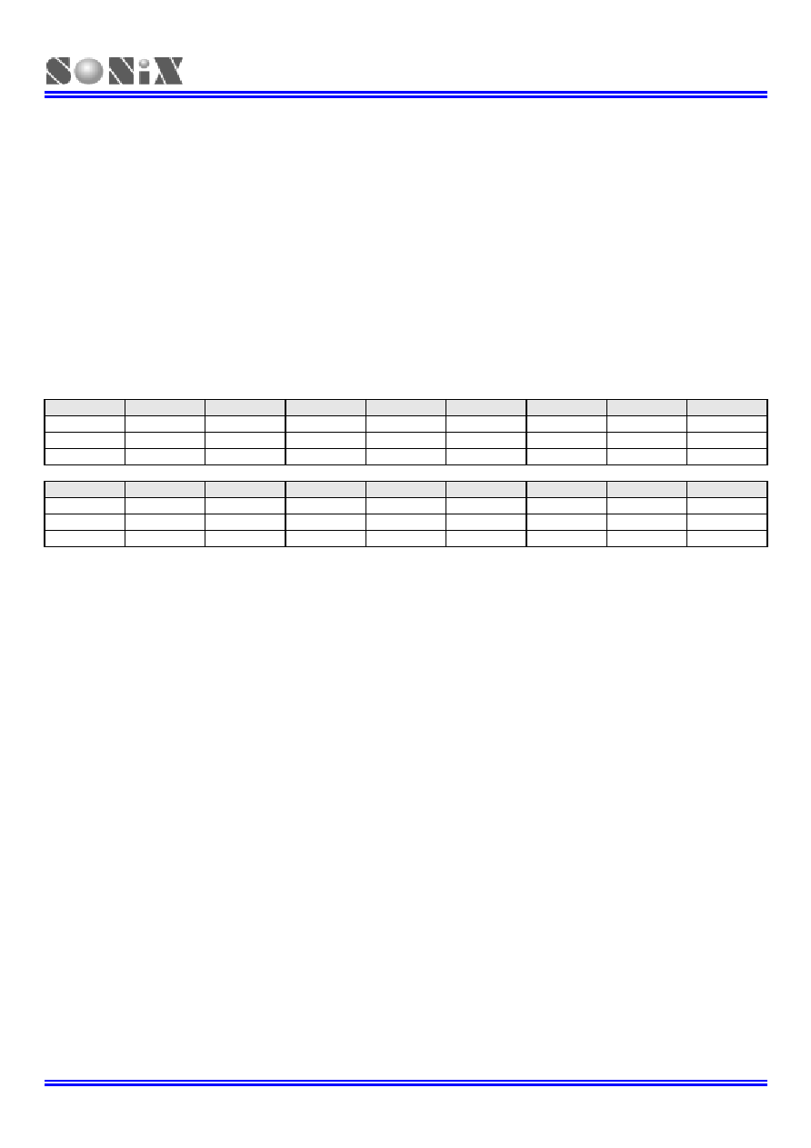
SELECTION TABLE
Timer
PWM Wakeup
CHIP
ROM RAM Stack
TC0 TC1
I/O
Green
Mode Buzzer Pin no.
Package
SN8P1602B 1K*16 48
4
V
-
14
V
-
6
DIP18/SOP18
/SSOP20
SN8P1602B
8-Bit Micro-Controller
SONiX TECHNOLOGY CO., LTD
Page 10
Version 1.1
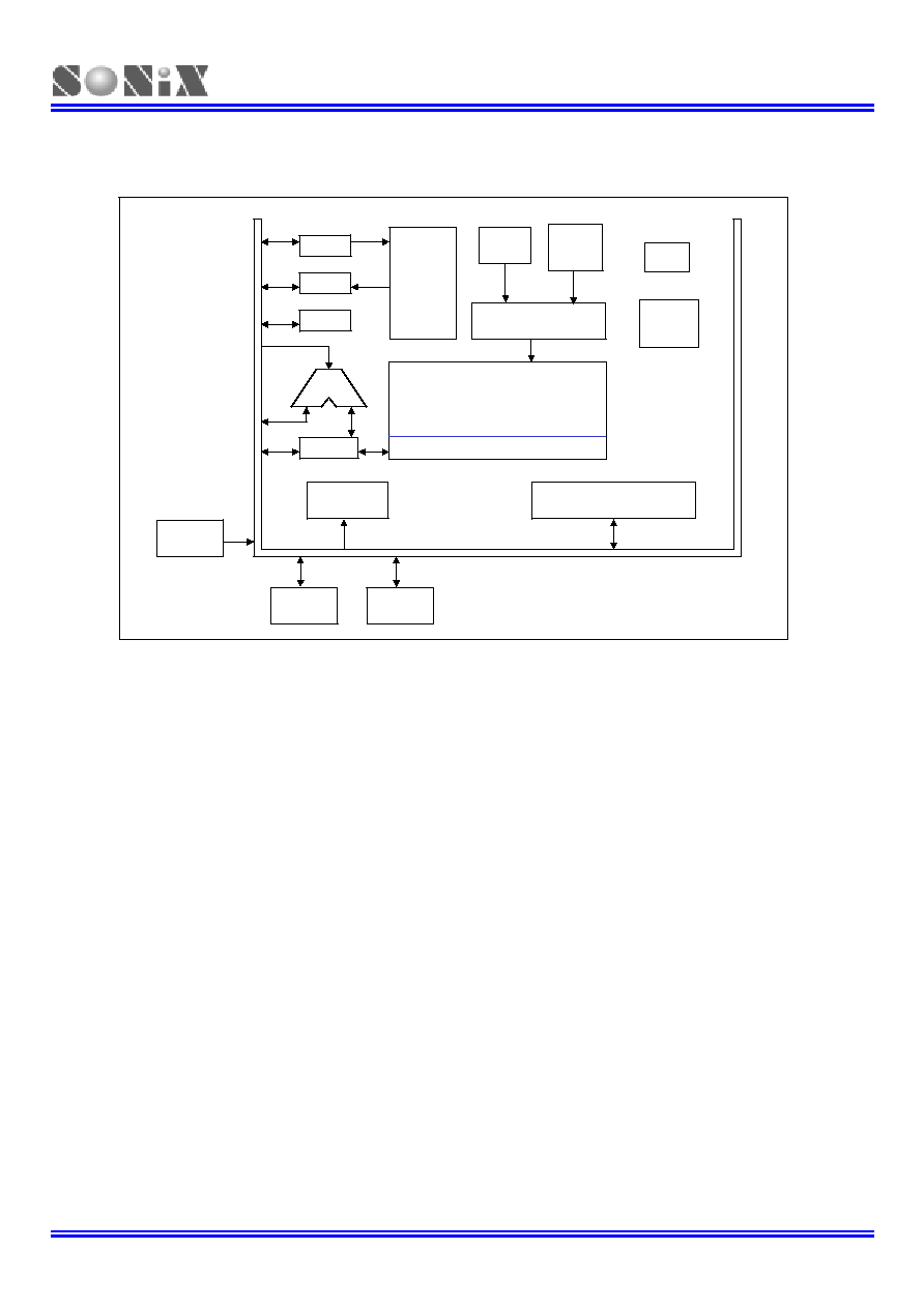
SYSTEM BLOCK DIAGRAM
SN8P1602B
PC
IR
ROM
H-OSC
TIMING GENERATOR
RAM
SYSTEM REGISTER
ALU
ACC
INTERRUPT
CONTROL
TIMER & COUNTER
PORT 0
PORT 2
PORT 1
FLAGS
Internal
RC
POR
Watch
Dog
PC
IR
ROM
H-OSC
TIMING GENERATOR
RAM
SYSTEM REGISTER
ALU
ACC
INTERRUPT
CONTROL
TIMER & COUNTER
PORT 0
PORT 2
PORT 1
FLAGS
Internal
RC
POR
Watch
Dog
PC
IR
ROM
H-OSC
TIMING GENERATOR
RAM
SYSTEM REGISTER
ALU
ACC
INTERRUPT
CONTROL
TIMER & COUNTER
PORT 0
PORT 2
PORT 1
FLAGS
Internal
RC
POR
Watch
Dog

SN8P1602B
8-Bit Micro-Controller
SONiX TECHNOLOGY CO., LTD
Page 11
Version 1.1
PIN ASSIGNMENT
OTP Type:
SN8P1602BP (P-DIP 18 pins)
SN8P1602BS (SOP 18 pins)
P1.2
1
U
18
P1.1
P1.3
2
17
P1.0
INT0/P0.0
3
16
XIN
RST/VPP
4
15
XOUT/P1.4
VSS
5
14
VDD
P2.0
6
13
P2.7
P2.1
7
12
P2.6
P2.2
8
11
P2.5
P2.3
9
10
P2.4
SN8P1602BP
SN8P1602BS
SN8P1602BX (SSOP 20 pins)
P1.2
1
U
20
P1.1
P1.3
2
19
P1.0
INT0/P0.0
3
18
XIN
RST/VPP
4
17
XOUT/P1.4
VSS
5
16
VDD
VSS
6
15
VDD
P2.0
7
14
P2.7
P2.1
8
13
P2.6
P2.2
9
12
P2.5
P2.3
10
11
P2.4
SN8P1602BX

SN8P1602B
8-Bit Micro-Controller
SONiX TECHNOLOGY CO., LTD
Page 12
Version 1.1
PIN DESCRIPTIONS
SN8P1602B
PAD NAME
TYPE
DESCRIPTION
VDD, VSS
P
Power supply input pins. Place the 0.1µF bypass capacitor between the VDD and VSS pin.
RST/VPP I,
P
RST: System reset input pin. Schmitt trigger structure, low active, normal stay to
"high".
VPP: OTP programming pin.
XIN
I
External oscillator input pin. RC mode input pin.
XOUT/P1.4
I/O External oscillator output pin. In RC mode is P1.4 I/O.
P0.0 / INT0
I
Port 0.0 and shared with INT0 trigger pin (Schmitt trigger) / Built-in pull-up resistors.
P1.0 ~ P1.4
I/O Port 1.0~Port 1.4 bi-direction pins / Built-in pull-up resistors.
P2.0 ~ P2.7
I/O Port 2.0~Port 2.7 bi-direction pins / Built-in pull-up resistors.
PIN CIRCUIT DIAGRAMS
SN8P1602B
Note: All of the latch output circuits are push-pull structures.
Port0 structure
PUR
PUR
PUR
PnM, PUR
Pin
PnM
Latch
Port1~Port2 structure
PnM
Pin
Int. bus
Port0 structure
PUR
PUR
PUR
PnM, PUR
Pin
PnM
Latch
Port1~Port2 structure
PnM
Pin
Int. bus
SN8P1602B
8-Bit Micro-Controller
SONiX TECHNOLOGY CO., LTD
Page 13
Version 1.1
2
2
2
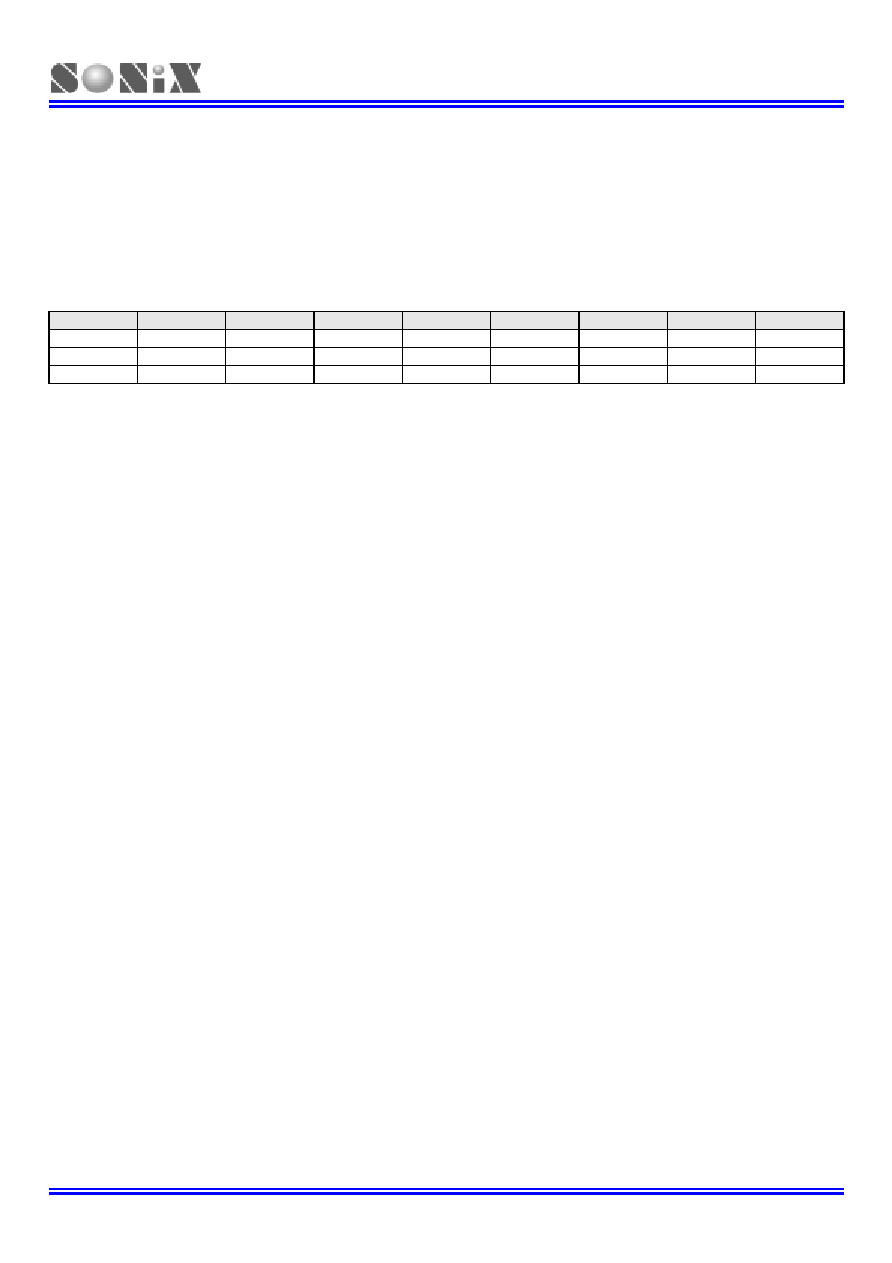
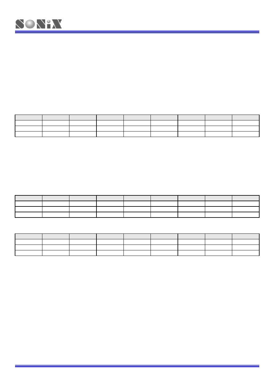
CODE OPTION TABLE
SN8P1602B
Code Option
Content
Function Description
RC
Low cost RC for external high clock oscillator
32K X'tal
Low frequency, power saving crystal (e.g. 32.768K) for external high
clock oscillator
12M X'tal
High speed crystal /resonator (e.g. 12M) for external high clock oscillator
High_Clk
4M X'tal
Standard crystal /resonator (e.g. 3.58M) for external high clock oscillator
Enable
External high clock divided by two, Fosc = high clock / 2
High_Clk / 2
Disable
Fosc = high clock
Enable
Enable Oscillator Safe Guard function to enhance noise immunity
performance.
OSG
Disable
Disable Oscillator Safe Guard function
Enable
Enable Watch Dog function
Watch_Dog
Disable
Disable Watch Dog function
Enable
Enable Low Power function to save Operating current
Low Power
Disable
Disable Low Power function
Enable
Enable Noise Filter function to enhance noise immunity performance
Noise Filter
Disable
Disable Noise Filter function
Enable
Enable ROM code Security function
Security
Disable
Disable ROM code Security function
Always_ON
Force Watch Dog Timer clock source come from INT 16K RC.
Also INT 16K RC never stop both in power down and green mode that
means Watch Dog Timer will always enable both in power down and
green mode.
INT_16K_RC
By_CPUM
Enable or Disable internal 16K(at 3V) RC clock by CPUM register
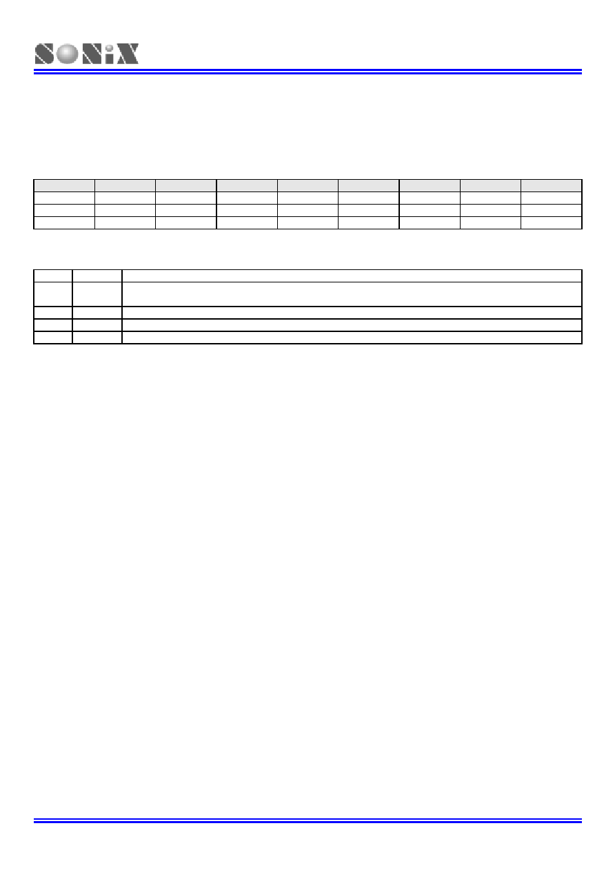
Table 2-1 SN8P1602B Code Option Table
This table is for design guidance, not tested or guaranteed. Some values presented are outside specified operating
range. This is for information only and devices are guaranteed to operate properly only within the specified range.
Code Option
Lowest Operation Voltage
Enable
Disable
4 MHz
16 MHz
-
Noise Filter/Low Power/OSG
2.2V
2.8V
Noise Filter
Low Power/OSG
2.2V
3.5V
Low Power
Noise Filter/OSG
2.2V
3.8V
OSG
Noise Filter/Low Power
2.2V
2.9V
Table 2-2 SN8P1602B Minimum Working Voltage vs. Code Option and clock frequency
Notice:
Under high noisy environment, enable "Noise Filter", "OSG" and disable "Low Power" is strongly
recommended.
The side effect is to increase the minimum working voltage if enables "Noise Filter"/"OSG"/ "Low Power"
code option. (Please refer to Characteristic Graphs)
Enable "Low Power" option will reduce operating current during the normal operating mode.
If users select "32K X'tal" in "High_Clk" option, assembler will force "OSG" to be enabled.
If users select "RC" in "High_Clk" option, assembler will force "High_Clk / 2" to be enabled.

SN8P1602B
8-Bit Micro-Controller
SONiX TECHNOLOGY CO., LTD
Page 14
Version 1.1
3
3
3
ADDRESS SPACES
PROGRAM MEMORY (ROM)
OVERVIEW
The SN8P1602B provides the program memory up to 1024 * 16-bit to be addressed and is able to fetch instructions
through 10-bit wide PC (Program Counter). It can look up ROM data by using ROM code registers (R, Y, Z).
1-word reset vector addresses
1-word interrupt vector addresses
1K words general purpose area
5-word reserved area
All of the program memory is partitioned into three coding areas. The first area is located from 00H to 03H(The Reset
vector area), the second area is a reserved area 04H ~07H, the 3
rd
area is for the interrupt vector and the user code
area from 0008H to 03FEH/0FFEH. The address 08H is the interrupt enter address point.
ROM
0000H
Reset vector
User reset vector
0001H
Jump to user start address
0002H
Jump to user start address
0003H
General purpose area
Jump to user start address
0004H
0005H
0006H
0007H
Reserved
0008H
Interrupt vector
User interrupt vector
0009H User
program
.
.
000FH
0010H
0011H
.
.
03FEH
General purpose area
End of user program
03FFH
Reserved

SN8P1602B
8-Bit Micro-Controller
SONiX TECHNOLOGY CO., LTD
Page 15
Version 1.1
USER RESET VECTOR ADDRESS (0000H)
A 1-word vector address area is used to execute system reset. After power on reset or watchdog timer overflow reset,
then the chip will restart the program from address 0000h and all system registers will be set as default values. The
following example shows the way to define the reset vector in the program memory.
Programming Tip: Defining Reset Vector
CHIP SN8P1602B
ORG
0
;
0000H
JMP
START
; Jump to user program address.
.
; 0004H ~ 0007H are reserved
ORG
10H
START:
; 0010H, The head of user program.
.
; User program
.
.
.
ENDP
; End of program
INTERRUPT VECTOR ADDRESS (0008H)
A 1-word vector address area is used to execute interrupt request. If any interrupt service executes, the program
counter (PC) value is stored in stack buffer and jump to 0008h of program memory to execute the vectored interrupt.
Users have to define the interrupt vector. The following example shows the way to define the interrupt vector in the
program memory.
Programming Tip: Defining Interrupt Vector (Example 1)
CHIP SN8P1602B
.DATA PFLAGBUF
.CODE
ORG
0
;
0000H
JMP
START
; Jump to user program address.
.
; 0004H ~ 0007H are reserved
ORG
8
; Interrupt service routine
B0XCH
A, ACCBUF
; B0XCH doesn't change C, Z flag
B0MOV
A,
PFLAG
B0MOV
PFLAGBUF, A
; Save PFLAG register in a buffer
.
.
B0MOV
A,
PFLAGBUF
B0MOV
PFLAG, A
; Restore PFLAG register from buffer
B0XCH
A, ACCBUF
; B0XCH doesn't change C, Z flag
RETI
; End of interrupt service routine
START:
; The head of user program.
.
; User program
.
JMP
START
; End of user program
ENDP
; End of program

SN8P1602B
8-Bit Micro-Controller
SONiX TECHNOLOGY CO., LTD
Page 16
Version 1.1
Programming Tip: Defining Interrupt Vector (Example 2)
CHIP SN8P1602B
.DATA PFLAGBUF
.CODE
ORG
0
;
0000H
JMP
START
; Jump to user program address.
.
; 0001H ~ 0007H are reserved
ORG
08
JMP
MY_IRQ
; 0008H, Jump to interrupt service routine address
ORG
10H
START:
; 0010H, The head of user program.
.
; User program
.
.
JMP
START
; End of user program
MY_IRQ:
;The head of interrupt service routine
B0XCH
A, ACCBUF
; B0XCH doesn't change C, Z flag
B0MOV
A,
PFLAG
B0MOV
PFLAGBUF, A
; Save PFLAG register in a buffer
.
.
B0MOV
A,
PFLAGBUF
B0MOV
PFLAG, A
; Restore PFLAG register from buffer
B0XCH
A, ACCBUF
; B0XCH doesn't change C, Z flag
RETI
; End of interrupt service routine
ENDP
; End of program
Remark: It is easy to understand the rules of SONIX program from demo programs given above. These
points are as following:
1. The address 0000H is a "JMP" instruction to make the program starts from the beginning.
2. The 0004H~0007H are reserved. Users is NOT allow to use 0004H~0007H addresses. The default
value might change from time to time during various production progress. We strongly suggest
users DO NOT take this value into the Check Sum. For detailed information, please check the
following Checksum Calculation section

SN8P1602B
8-Bit Micro-Controller
SONiX TECHNOLOGY CO., LTD
Page 17
Version 1.1
CHECKSUM CALCULATION
The ROM addresses 0004H~0007H and last address are reserved area. User should avoid these addresses
(0004H~0007H and last address) when calculate the Checksum value.
Example:
The demo program shows how to avoid 0004H~0007H when calculated Checksum from 00H to the end of
user's code
MOV
A,#END_USER_CODE$L
B0MOV
END_ADDR1,A
;save low end address to end_addr1
MOV
A,#END_USER_CODE$M
B0MOV
END_ADDR2,A
;save middle end address to end_addr2
CLR
Y
;set Y to 00H
CLR
Z
;set Z to 00H
@@:
CALL
YZ_CHECK
;call function of check yz value
MOVC
;
B0BSET
FC ;clear
C
flag
ADD
DATA1,A
;add A to Data1
MOV
A,R
ADC
DATA2,A
;add R to Data2
JMP
END_CHECK
;check if the YZ address = the end of code
AAA:
INCMS
Z
;Z=Z+1
JMP
@B
;if Z!= 00H calculate to next address
JMP
Y_ADD_1
;if Z=00H increase Y
END_CHECK:
MOV
A,END_ADDR1
CMPRS
A,Z
;check if Z = low end address
JMP
AAA
;if Not jump to checksum calculate
MOV
A,END_ADDR2
CMPRS
A,Y
;if Yes, check if Y = middle end address
JMP
AAA
;if Not jump to checksum calculate
JMP
CHECKSUM_END
;if Yes checksum calculated is done.
YZ_CHECK:
;check if YZ=0004H
MOV
A,#04H
CMPRS
A,Z
;check if Z=04H
RET
;if Not return to checksum calculate
MOV
A,#00H
CMPRS
A,Y
;if Yes, check if Y=00H
RET
;if Not return to checksum calculate
INCMS
Z
;if Yes, increase 4 to Z
INCMS
Z
INCMS
Z
INCMS
Z
RET
;set YZ=0008H then return
Y_ADD_1:
INCMS
Y
;increase
Y
NOP
JMP
@B
;jump to checksum calculate
CHECKSUM_END:
..........
..........
END_USER_CODE:
;Label of program end

SN8P1602B
8-Bit Micro-Controller
SONiX TECHNOLOGY CO., LTD
Page 18
Version 1.1
GENERAL PURPOSE PROGRAM MEMORY AREA
The ROM location 0009H~03FEH are used as general-purpose memory. The area is to store both instruction's
op-code and look-up table data. The SN8P1602B includes jump table function by using program counter (PC) and
look-up table function by using ROM code registers (R, Y, Z).
The boundary of program memory is separated by the high-byte program counter (PCH) every 100H. In jump table
function and look-up table function, the program counter can't leap over the boundary by program counter
automatically. Users need to modify the PCH value to "PCH+1" when the PCL overflows (from 0FFH to 000H).
LOOK-UP TABLE DESCRIPTION
In the ROM's data lookup function, Y register is pointed to the bit 8~bit 15 and Z register to the bit 0~bit 7 data of ROM
address. After MOVC instruction is executed, the low-byte data will be stored in ACC and high-byte data stored in R
register.
Example: To look up the ROM data located "TABLE1".
B0MOV
Y, #TABLE1$M
; To set lookup table1's middle address
B0MOV
Z, #TABLE1$L
; To set lookup table1's low address.
MOVC
; To lookup data, R = 00H, ACC = 35H
;
; Increment the index address for next address
INCMS Z
;
Z+1
JMP
@F
; Not overflow
INCMS
Y
; Z overflow (FFH 00), Y=Y+1
NOP
;
;
@@:
MOVC
; To lookup data, R = 51H, ACC = 05H.
.
.
;
TABLE1:
DW
0035H
; To define a word (16 bits) data.
DW
5105H
; "
DW
2012H
; "
CAUSION: The Y register will not increase automatically when Z register crosses boundary from 0xFF to
0x00. Therefore, user must take care
such
situation to avoid
loop-up table errors.
If
Z
register
overflows, Y register must be added one. The following INC_YZ macro shows a simple method to process
Y and Z registers automatically.
Note: Because the program counter (PC) is only 12-bit, the X register is useless in the application. Users
can omit "B0MOV X, #TABLE1$H". SONiX ICE supports larger program memory addressing capability.
Please be sure that X register is "0" to avoid unpredicted error in loop-up table operation.
Example: INC_YZ Macro
INC_YZ
MACRO
INCMS
Z
; Z+1
JMP
@F
; Not overflow
INCMS
Y
; Y+1
NOP
; Not overflow
@@:
ENDM

SN8P1602B
8-Bit Micro-Controller
SONiX TECHNOLOGY CO., LTD
Page 19
Version 1.1
The other example of loop-up table is to add Y or Z index register by accumulator. Please be careful if "carry" happen.
Example: Increase Y and Z register by B0ADD/ADD instruction
B0MOV
Y, #TABLE1$M
; To set lookup table's middle address.
B0MOV
Z, #TABLE1$L
; To set lookup table's low address.
B0MOV
A, BUF
; Z = Z + BUF.
B0ADD Z,
A
B0BTS1
FC
; Check the carry flag.
JMP
GETDATA
; FC = 0
INCMS
Y
; FC = 1. Y+1.
NOP
GETDATA:
;
MOVC
; To lookup data. If BUF = 0, data is 0x0035
; If BUF = 1, data is 0x5105
; If BUF = 2, data is 0x2012
.
.
.
.
;
TABLE1:
DW
0035H
; To define a word (16 bits) data.
DW
5105H
; "
DW
2012H
; "

SN8P1602B
8-Bit Micro-Controller
SONiX TECHNOLOGY CO., LTD
Page 20
Version 1.1
JUMP TABLE DESCRIPTION
The jump table operation is one of multi-address jumping function. Add low-byte program counter (PCL) and ACC
value to get one new PCL. The new program counter (PC) points to a series jump instructions as a listing table. It is
easy to make a multi-jump program depends on the value of the accumulator (A).
When carry flag occurs after executing of "ADD PCL, A", it will not affect PCH register. Users have to check if the jump
table crosses over the ROM page boundary or the listing file generated by SONIX assembly software. We suggest
users to place the jump table at the beginning of the program memory page (xx00H) to avoid errors to occur when
editing the program.
Example :
ORG
0X0100
; The jump table is from the head of the ROM boundary
B0ADD
PCL, A
; PCL = PCL + ACC, the PCH can't be changed.
JMP
A0POINT
; ACC = 0, jump to A0POINT
JMP
A1POINT
; ACC = 1, jump to A1POINT
JMP
A2POINT
; ACC = 2, jump to A2POINT
JMP
A3POINT
; ACC = 3, jump to A3POINT
In following example, the jump table starts at 0x00FD. When execute B0ADD PCL, A. If ACC = 0 or 1, the jump
table points to the right address. If the ACC is larger then 1 will cause error because PCH doesn't increase one
automatically. We can see the PCL = 0 when ACC = 2 but the PCH still keep in 0. The program counter (PC) will
enter
the wrong address 0x0000 and the system will be in a unexpected operation mode. It
is important to check whether the jump table crosses over the boundary (xxFFH to xx00H). A good coding
style is to put the jump table at the start of ROM boundary (e.g. 0100H).
Example (Incorrect): If the "jump table" crosses over ROM boundary, the program will cause the
errors to occur.
ROM Address
. .
. .
. .
0X00FD
B0ADD
PCL, A
; PCL = PCL + ACC, the PCH can't be changed.
0X00FE
JMP
A0POINT
; ACC = 0
0X00FF
JMP
A1POINT
; ACC = 1
0X0100
JMP
A2POINT
; ACC = 2
jump table cross boundary here
0X0101
JMP
A3POINT
; ACC = 3
. .
. .
SONIX provides a macro for safe jump table function. This macro will check the ROM boundary and move the jump
table to the right position automatically. The side effect of this macro maybe wastes some ROM size.
@JMP_A MACRO
VAL
IF
(($+1) !& 0XFF00) !!= (($+(VAL)) !& 0XFF00)
JMP
($ | 0XFF)
ORG
($ | 0XFF)
ENDIF
ADD
PCL,
A
ENDM
Note: "VAL" is the number of the jump table listing number.

SN8P1602B
8-Bit Micro-Controller
SONiX TECHNOLOGY CO., LTD
Page 21
Version 1.1
Example: "@JMP_A" application in SONIX macro file called "MACRO3.H".
B0MOV
A, BUF0
; "BUF0" is from 0 to 4.
@JMP_A
5
; The number of the jump table listing is five.
JMP
A0POINT
; If ACC = 0, jump to A0POINT
JMP
A1POINT
; ACC = 1, jump to A1POINT
JMP
A2POINT
; ACC = 2, jump to A2POINT
JMP
A3POINT
; ACC = 3, jump to A3POINT
JMP
A4POINT
; ACC = 4, jump to A4POINT
If the jump table position is from 00FDH to 0101H, the "@JMP_A" macro will make the jump table to start from 0100h.

SN8P1602B
8-Bit Micro-Controller
SONiX TECHNOLOGY CO., LTD
Page 22
Version 1.1
DATA MEMORY (RAM)
OVERVIEW
The SN8P1602B has internally built-in data memory up to 48 bytes for storing the general-purpose data.
48 * 8-bit RAM
The memory is separated into bank 0. The bank 0 uses the first 48 bytes as general-purpose area, and the remaining
128 bytes area as system register.
SN8P1602B
RAM location
000h
"
"
000h~02FH/07FH of Bank 0 store
general-purpose data (48 bytes
/128bytes).
"
"
"
02Fh
General purpose area
080h
"
080h~0FFh of Bank 0 store system
registers (128 bytes).
"
"
"
"
System register
BANK 0
0FFh
End of bank 0 area
SN8P1602B
8-Bit Micro-Controller
SONiX TECHNOLOGY CO., LTD
Page 23
Version 1.1
WORKING REGISTERS
These Y,Z registers can be used as the general-purpose working buffer or access ROM's and RAM's data. For
instance, all of the ROM table can be looked-up by Y and Z registers. The data of RAM memory can be indirectly
accessed with Y and Z registers.
Y, Z REGISTERS
The Y and Z registers are the 8-bit buffers. There are three major functions of these registers.
can be used as general working registers
can be used as RAM data pointers with @YZ register
can be used as ROM data pointer with the MOVC instruction for look-up table
084H
Bit 7
Bit 6
Bit 5
Bit 4
Bit 3
Bit 2
Bit 1
Bit 0
Y
YBIT7 YBIT6 YBIT5 YBIT4 YBIT3 YBIT2 YBIT1 YBIT0
Read/Write R/W
R/W
R/W R/W R/W R/W R/W R/W
After
reset
0 0 0 0 0 0 0 0
083H
Bit 7
Bit 6
Bit 5
Bit 4
Bit 3
Bit 2
Bit 1
Bit 0
Z
ZBIT7 ZBIT6 ZBIT5 ZBIT4 ZBIT3 ZBIT2 ZBIT1 ZBIT0
Read/Write R/W
R/W
R/W R/W R/W R/W R/W R/W
After
reset
0 0 0 0 0 0 0 0
Example: uses YZ register as the data pointer to access data in the RAM address 025H of bank0.
B0MOV
Y, #00H
; To set RAM bank 0 for Y register
B0MOV
Z, #25H
; To set location 25H for Z register
B0MOV
A, @YZ
; To read a data into ACC
Example: uses the YZ register as data pointer to clear the RAM data
B0MOV
Y, #0
; Y = 0, bank 0
B0MOV
Z, #07FH
; Y = 7FH, the last address of the data memory area
CLR_YZ_BUF:
CLR
@YZ
; Clear @YZ to be zero
DECMS
Z
; Z ≠ 1, if Z= 0, finish the routine
JMP
CLR_YZ_BUF
; Not zero
CLR
@YZ
END_CLR:
; End of clear general purpose data memory area of bank 0
.
SN8P1602B
8-Bit Micro-Controller
SONiX TECHNOLOGY CO., LTD
Page 24
Version 1.1
R REGISTERS
R register is an 8-bit buffer. There are two major functions of the register.
can be used as working register
for store high-byte data of look-up table
(MOVC instruction executed, the high-byte data of specified ROM address will be stored in R register and the
low-byte data will be stored in ACC).
082H
Bit 7
Bit 6
Bit 5
Bit 4
Bit 3
Bit 2
Bit 1
Bit 0
R
RBIT7 RBIT6 RBIT5 RBIT4 RBIT3 RBIT2 RBIT1 RBIT0
Read/Write R/W
R/W
R/W R/W R/W R/W R/W R/W
After
reset
0 0 0 0 0 0 0 0
Note: Please refer to the "LOOK-UP TABLE DESCRIPTION" about R register look-up table application.
SN8P1602B
8-Bit Micro-Controller
SONiX TECHNOLOGY CO., LTD
Page 25
Version 1.1
PROGRAM FLAG
The PFLAG includes carry flag (C), decimal carry flag (DC) and zero flag (Z). If the result of operating is zero or there is
carry, borrow occurrence, then these flags will be set to PFLAG register.
086H
Bit 7
Bit 6
Bit 5
Bit 4
Bit 3
Bit 2
Bit 1
Bit 0
PFLAG
NT0 NPD -
-
-
C DC Z
Read/Write
R/W R/W -
-
- R/W R/W R/W
After
reset
- - - - - 0 0 0
RESET/WAKEUP FLAG
NT0 NPD Description
0 0
During the sleep mode, the device wakes up by the watch dog.
Such function only valid when users set "INT_16K_RC" code option as "Always_On"
0
1
Watchdog timer overflow in normal/slow/green mode.
1
0
During the sleep mode, the device wakes up by the reset pin.
1
1
External reset or LVD reset active
Note: Watchdog timer can also be used as a fixed-period timer if the watchdog reset function has been disabled.
CARRY FLAG
C = 1: When executed arithmetic addition with overflow or executed arithmetic subtraction without borrow or executed
rotation instruction with logic "1" shifting out.
C = 0: When executed arithmetic addition without overflow or executed arithmetic subtraction with borrow or executed
rotation instruction with logic "0" shifting out.
DECIMAL CARRY FLAG
DC = 1: If executed arithmetic addition with overflow of low nibble or executed arithmetic subtraction without borrow of
low nibble.
DC = 0: If executed arithmetic addition without overflow of low nibble or executed arithmetic subtraction with borrow of
low nibble.
ZERO FLAG
Z = 1: When the content of ACC or target memory is zero after executing instructions involving a zero flag.
Z = 0: When the content of ACC or target memory is not zero after executing instructions involving a zero flag.

SN8P1602B
8-Bit Micro-Controller
SONiX TECHNOLOGY CO., LTD
Page 26
Version 1.1
ACCUMULATOR
The ACC is an 8-bit data register responsible for transferring or manipulating data between ALU and data memory. If
the result of operating is zero (Z) or there is carry (C or DC) occurrence, then these flags will be set to PFLAG register.
ACC is not in data memory (RAM), so ACC can't be access by "B0MOV" instruction during the instant addressing
mode.
Example: Read and write ACC value.
; Read ACC data and store in BUF data memory
MOV
BUF,
A
; Write a immediate data into ACC
MOV
A,
#0FH
; Write ACC data from BUF data memory
MOV
A,
BUF
The system doesn't store ACC and PFLAG value when interrupt executed. ACC and PFLAG data must be saved to
other data memories.
Example: Protect ACC and working registers.
ACCBUF
EQU
00H
; ACCBUF is ACC data buffer.
PFLAGBUF
EQU
01H
; PFLAGBUF is PFLAG data buffer.
INT_SERVICE:
B0XCH
A, ACCBUF
; Store ACC value
B0MOV
A, PFLAG
; Store PFLAG value
B0MOV
PFLAGBUF,A
.
.
.
.
B0MOV
A, PFLAGBUF
; Re-load PFLAG value
B0MOV
PFLAG,A
B0XCH
A, ACCBUF
; Re-load ACC by B0XCH command, and which will not
affect the PFLAG again.
RETI
; Exit interrupt service vector
Note: To save and re-load ACC data, users must use "B0XCH" instruction, or else the PFLAG Register
might be modified by ACC operation.
SN8P1602B
8-Bit Micro-Controller
SONiX TECHNOLOGY CO., LTD
Page 27
Version 1.1
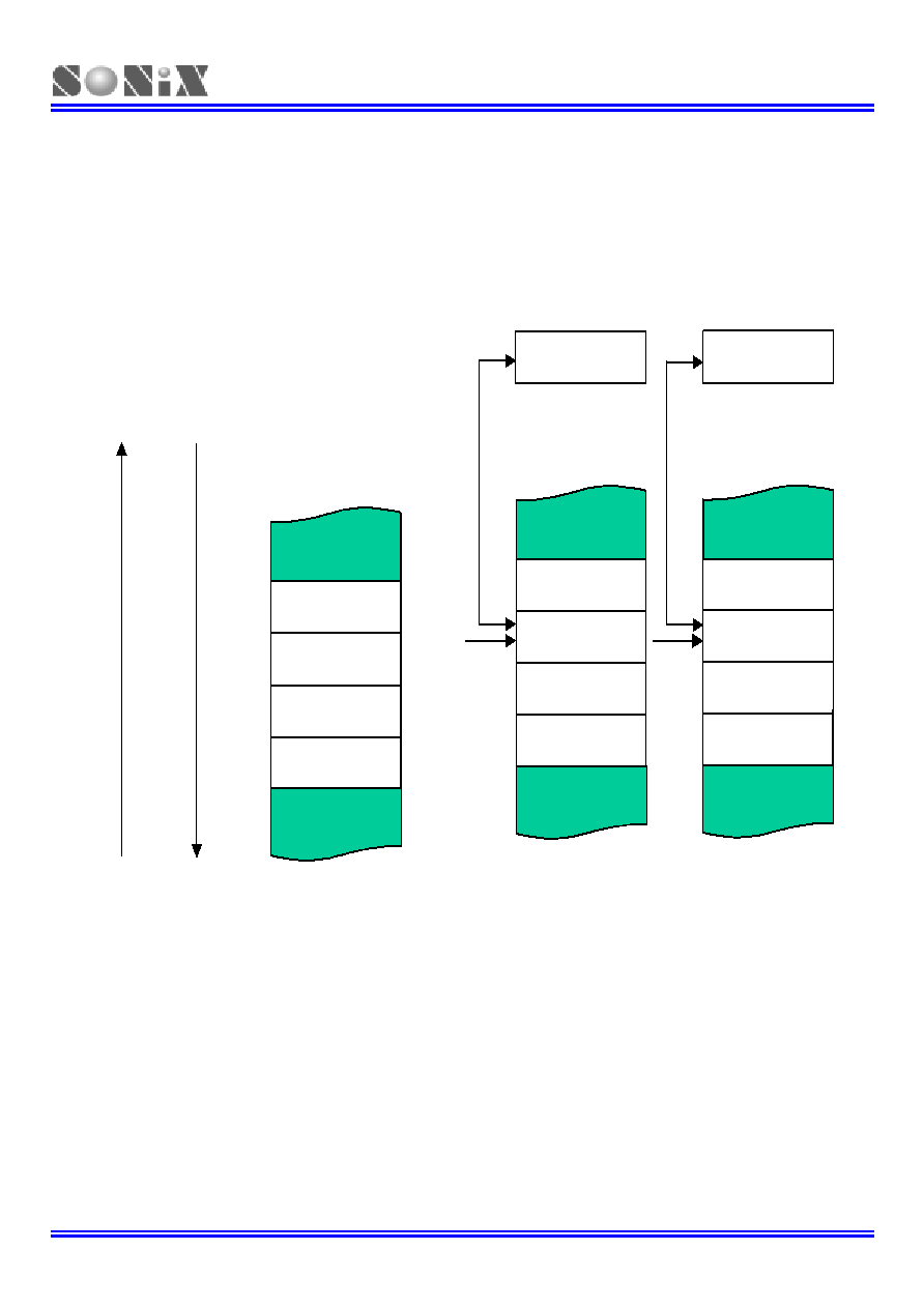
STACK OPERATIONS
OVERVIEW
The stack buffer of SN8P1602B has 4-level. These buffers are designed to push and pop up program counter's (PC)
data when interrupt service routine is executed. The STKP register is a pointer designed to point active level in order to
push or pop up data from stack buffer. The STKnH and STKnL are the stack buffers to store program counter (PC)
data.
STKP = 0
STKP = 1
STKP = 2
STKP = 3
STKP -1
STKP + 1
CALL /
interrupt
RET /
RETI
STKP
PCH
PCL
STKP
STK0H
STK1H
STK2H
STK3H
STK0L
STK1L
STK2L
STK3L
STKP = 0
STKP = 1
STKP = 2
STKP = 3
STKP = 0
STKP = 1
STKP = 2
STKP = 3
STKP -1
STKP + 1
CALL /
interrupt
RET /
RETI
STKP -1
STKP + 1
STKP -1
STKP -1
STKP + 1
CALL /
interrupt
RET /
RETI
STKP
STKP
PCH
PCL
PCH
PCH
PCL
PCL
STKP
STKP
STK0H
STK1H
STK2H
STK3H
STK0L
STK1L
STK2L
STK3L
SN8P1602B
8-Bit Micro-Controller
SONiX TECHNOLOGY CO., LTD
Page 28
Version 1.1
STACK REGISTERS
The stack pointer (STKP) is a 3-bit register to store the address used to access the stack buffer, 10-bit data memory
(STKnH and STKnL) set aside for temporary storage of stack addresses.
The two stack operations are writing to the top of the stack (push) and reading from the top of stack (pop). Push
operation decrements the STKP and the pop operation increments each time. That makes the STKP always point to
the top address of stack buffer and write the last program counter value (PC) into the stack buffer.
The program counter (PC) value is stored in the stack buffer before a CALL instruction executed or during interrupt
service routine. Stack operation is a LIFO type (Last in and first out). The stack pointer (STKP) and stack buffer
(STKnH and STKnL) are located in the system register area bank 0.
SN8P1602B
0DFH
Bit 7
Bit 6
Bit 5
Bit 4
Bit 3
Bit 2
Bit 1
Bit 0
STKP
GIE
- - - -
STKPB2
STKPB1
STKPB0
Read/Write
R/W
- - - -
R/W
R/W
R/W
After
reset
0 - - - - 1 1 1
STKPBn: Stack pointer (n = 0 ~ 2)
GIE: Global interrupt control bit. 0 = disable, 1 = enable. Please refer to the interrupt chapter.
Example: Stack pointer (STKP) reset, we strongly recommended to clear the stack pointers in the
beginning of the program.
MOV
A,
#00000111B
B0MOV
STKP,
A
SN8P1602B
0F0H~0FFH
Bit 7
Bit 6
Bit 5
Bit 4
Bit 3
Bit 2
Bit 1
Bit 0
STKnH
- - - - - -
SnPC9
SnPC8
Read/Write
- - - - - -
R/W
R/W
After
reset
- - - - - - 0 0
STKn = <STKnH , STKnL> (n = 3 ~ 0)
SN8P1602B
0F0H~0FFH
Bit 7
Bit 6
Bit 5
Bit 4
Bit 3
Bit 2
Bit 1
Bit 0
STKnL
SnPC7 SnPC6 SnPC5 SnPC4 SnPC3 SnPC2 SnPC1 SnPC0
Read/Write R/W
R/W
R/W R/W R/W R/W R/W R/W
After
reset
0 0 0 0 0 0 0 0
For SN8P1602B : STKn = <STKnH , STKnL> (n = 3 ~ 0)
SN8P1602B
8-Bit Micro-Controller
SONiX TECHNOLOGY CO., LTD
Page 29
Version 1.1
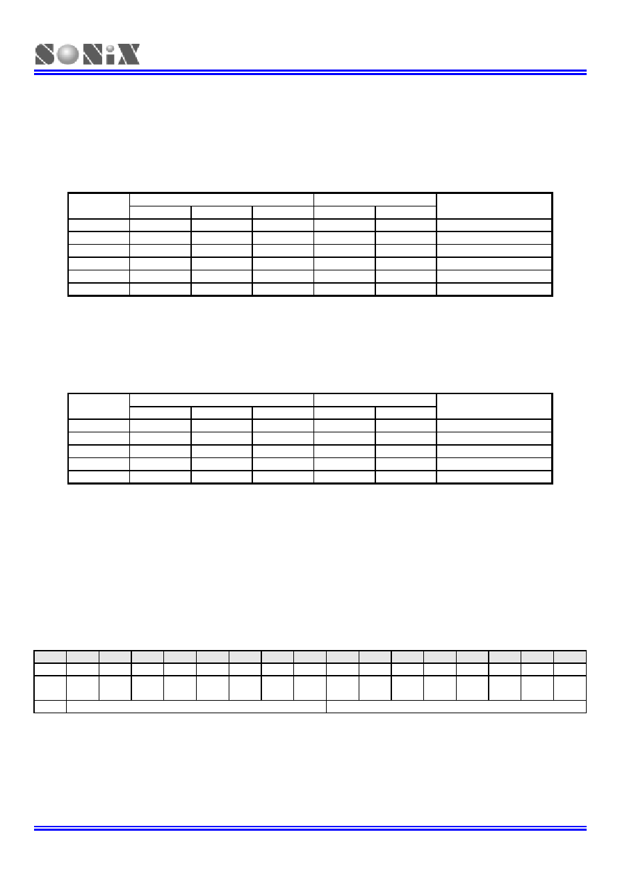
STACK OPERATION EXAMPLE
The two kinds of Stack-Save operations refer to the stack pointer (STKP) and write the content of program counter (PC)
to the stack buffer are CALL instruction and interrupt service. Under each condition, the STKP decreases and points to
the next available stack location. The stack buffer stores the program counter about the op-code address. The
Stack-Save operation is as the following table.
SN8P1602B
STKP Register
Stack Buffer
Stack Level
STKPB2 STKPB1 STKPB0 High
Byte
Low
Byte
Description
0
1 1 1
Free
Free
-
1
1 1 0
STK0H
STK0L
-
2
1 0 1
STK1H
STK1L
-
3
1 0 0
STK2H
STK2L
-
4
0 1 1
STK3H
STK3L
-
> 4
0 1 0 - -
Stack Over, error
There are Stack-Restore operations correspond to each push operation to restore the program counter (PC). The RETI
instruction uses for interrupt service routine. The RET instruction is for CALL instruction. When a pop operation occurs,
the STKP is incremented and points to the next free stack location. The stack buffer restores the last program counter
(PC) to the program counter registers. The Stack-Restore operation is as the following table.
SN8P1602B
STKP Register
Stack Buffer
Stack Level
STKPB2 STKPB1 STKPB0 High
Byte
Low
Byte
Description
4
0 1 1
STK3H
STK3L
-
3
1 0 0
STK2H
STK2L
-
2
1 0 1
STK1H
STK1L
-
1
1 1 0
STK0H
STK0L
-
0
1 1 1
Free
Free
-
PROGRAM COUNTER
The program counter (PC) is a 10-bit binary counter separated into the high-byte 2 and the low-byte 8 bits. This
counter is responsible for pointing a location in order to fetch an instruction for kernel circuit. Normally, the program
counter is automatically incremented with each instruction during program execution.
Besides, it can be replaced with specific address by executing CALL or JMP instruction. When JMP or CALL instruction
is executed, the destination address will be inserted to bit 0 ~ bit 9.
SN8P1602B
Bit 15 Bit 14 Bit 13 Bit 12 Bit 11 Bit 10 Bit 9 Bit 8
Bit 7 Bit 6 Bit 5 Bit 4 Bit 3 Bit 2
Bit 1 Bit 0
PC
- - - - - -
PC9
PC8
PC7
PC6
PC5
PC4
PC3
PC2
PC1
PC0
After
reset
- - - - - - 0 0 0 0 0 0 0 0 0 0
PCH
PCL

SN8P1602B
8-Bit Micro-Controller
SONiX TECHNOLOGY CO., LTD
Page 30
Version 1.1
ONE ADDRESS SKIPPING
There are nine instructions (CMPRS, INCS, INCMS, DECS, DECMS, BTS0, BTS1, B0BTS0, B0BTS1) with one
address skipping function. If the result of these instructions is true, the PC will add 2 steps to skip next instruction.
If the condition of bit test instruction is true, the PC will add 2 steps to skip next instruction.
B0BTS1
FC
; To skip, if Carry_flag = 1
JMP
C0STEP
; Else jump to C0STEP.
.
C0STEP: NOP
B0MOV
A, BUF0
; Move BUF0 value to ACC.
B0BTS0
FZ
; To skip, if Zero flag = 0.
JMP
C1STEP
; Else jump to C1STEP.
.
C1STEP: NOP
If the ACC is equal to the immediate data or memory, the PC will add 2 steps to skip next instruction.
CMPRS
A, #12H
; To skip, if ACC = 12H.
JMP
C0STEP
; Else jump to C0STEP.
.
C0STEP: NOP
If the destination increased by 1, which results overflow of 0xFF to 0x00, the PC will add 2 steps to skip next
instruction.
INCS instruction:
INCS
BUF0
JMP
C0STEP
; Jump to C0STEP if ACC is not zero.
...
C0STEP: NOP
INCMS instruction:
INCMS
BUF0
JMP
C0STEP
; Jump to C0STEP if BUF0 is not zero.
...
C0STEP: NOP
If the destination decreased by 1, which results underflow of 0x00 to 0xFF, the PC will add 2 steps to skip next
instruction.
DECS instruction:
DECS
BUF0
JMP
C0STEP
; Jump to C0STEP if ACC is not zero.
...
C0STEP: NOP
DECMS instruction:
DECMS
BUF0
JMP
C0STEP
; Jump to C0STEP if BUF0 is not zero.
...
C0STEP: NOP

SN8P1602B
8-Bit Micro-Controller
SONiX TECHNOLOGY CO., LTD
Page 31
Version 1.1
MULTI-ADDRESS JUMPING
Users can jump around the multi-address by either JMP instruction or ADD M, An instruction (M = PCL) to activate
multi-address jumping function. If carry flag occurs after execution of ADD PCL, A, the carry flag will not affect PCH
register.
Example: If PC = 0323H (PCH = 03H
PCL = 23H)
; PC = 0323H
MOV
A,
#28H
B0MOV
PCL, A
; Jump to address 0328H
.
.
.
.
; PC = 0328H
.
.
MOV
A,
#00H
B0MOV
PCL, A
; Jump to address 0300H
Example: If PC = 0323H (PCH = 03H
PCL = 23H)
; PC = 0323H
B0ADD
PCL, A
; PCL = PCL + ACC, the PCH cannot be changed.
JMP
A0POINT
; If ACC = 0, jump to A0POINT
JMP
A1POINT
; ACC = 1, jump to A1POINT
JMP
A2POINT
; ACC = 2, jump to A2POINT
JMP
A3POINT
; ACC = 3, jump to A3POINT
.
.
;

SN8P1602B
8-Bit Micro-Controller
SONiX TECHNOLOGY CO., LTD
Page 32
Version 1.1
4
4
4
ADDRESSING MODE
OVERVIEW
The SN8P1602B provides three addressing modes to access RAM data, including immediate addressing mode,
directly addressing mode and indirectly address mode.
IMMEDIATE ADDRESSING MODE
The immediate addressing mode uses an immediate data to set up the location (" MOV A, # I ", " B0MOV M, # I ") in
ACC or specific RAM.
Immediate addressing mode
MOV
A, #12H
; To set an immediate data 12H into ACC
DIRECTLY ADDRESSING MODE
The directly addressing mode moves the content of RAM location in or out of ACC.(" MOV A,12H ", " MOV 12H,
A ").
Directly addressing mode
B0MOV
A, 12H
; To get a content of location 12H of bank 0 and save in ACC
INDIRECTLY ADDRESSING MODE
The indirectly addressing mode is to access the memory by the data pointer registers (Y/Z).
Example: Indirectly addressing mode with @YZ register
CLR
Y
; To clear Y register to access RAM bank 0.
B0MOV
Z, #12H
; To set an immediate data 12H into Z register.
B0MOV
A, @YZ
; Use data pointer @YZ reads a data from RAM location
; 012H into ACC.
SN8P1602B
8-Bit Micro-Controller
SONiX TECHNOLOGY CO., LTD
Page 33
Version 1.1
5
5
5
SYSTEM REGISTER
OVERVIEW
The RAM area located in 80H~FFH bank 0 is system register area. The main purpose of system registers is to control
peripheral hardware of the chip. Using system registers can control I/O ports, timers and counters by programming.
The memory map provides an easy and quick reference source for writing application program. These system registers
accessing is controlled by the selected memory bank (RBANK = 0) or the bank 0 read/write instruction (B0MOV,
B0BSET, B0BCLR...).
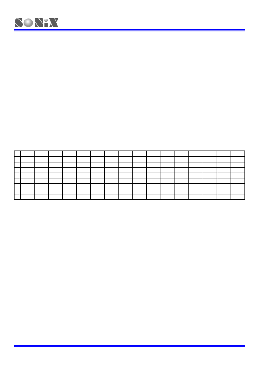
SYSTEM REGISTER ARRANGEMENT (BANK 0)
BYTES of SYSTEM REGISTER
SN8P1602B
0 1 2 3 4 5 6 7 8 9 A B C D E F
8
- - R Z Y -
PFLAG RPAGE
- - - - - - - -
9
- - - - - - - - - - - - - - - -
A
- - - - - - - - - - - - - - - -
B
- - - - - - - - - - - - - -
PUR
PEDGE
C
P1W
P1M
P2M
- - - - -
INTRQ INTEN OSCM
- - -
PCL
PCH
D
P0
P1
P2 - - - - -
T0M
-
TC0M
TC0C
- - -
STKP
E
- - - - - - -
@YZ
- - - - - - - -
F
- - - - - - - -
STK3L STK3H STK2L STK2H
STK1L
STK1H STK0L STK0H
Description
PFLAG = ROM page and special flag register.
R = Working register and ROM look-up data buffer.
P1W = Port 1 wakeup register.
Y, Z = Working, @YZ and ROM addressing register.
PnM = Port n input/output mode register.
Pn = Port n data buffer.
INTRQ = Interrupt request register.
INTEN = Interrupt enable register.
OSCM = Oscillator mode register.
PCH, PCL = Program counter.
TCnM = Timer n mode register.
TCnC = Timer n counting register.
T0M.1= TC0GN, TC0 green mode wakeup flag.
STKP = Stack pointer buffer.
STK0~STK3 = Stack 0 ~ stack 3 buffer.
@YZ = RAM YZ indirect addressing index pointer.
SN8P1602B
8-Bit Micro-Controller
SONiX TECHNOLOGY CO., LTD
Page 34
Version 1.1
BITS of SYSTEM REGISTER
SN8P1602B system register table
Address
Bit7 Bit6 Bit5 Bit4 Bit3 Bit2 Bit1 Bit0
R/W Remarks
082H RBIT7 RBIT6 RBIT5 RBIT4 RBIT3 RBIT2 RBIT1 RBIT0 R/W
R
083H ZBIT7 ZBIT6 ZBIT5 ZBIT4 ZBIT3 ZBIT2 ZBIT1 ZBIT0
R/W
Z
084H YBIT7 YBIT6 YBIT5 YBIT4 YBIT3 YBIT2 YBIT1 YBIT0 R/W
Y
086H NT0 NPD -
-
-
C
DC
Z R/W
PFLAG
0BEH
- - - - -
PUR2
PUR1
PUR0
W
PUR
0BFH
PEDGEN -
- P00G1
P00G0 -
-
- W
PEDGE
0C0H 0
0
0 P14W P13W P12W P11W P10W
R/W
P1W
wakeup
register
0C1H 0
0
0 P14M P13M P12M P11M P10M
R/W
P1M
I/O
direction
0C2H P27M P26M P25M P24M P23M P22M P21M P20M
R/W
P2M
I/O
direction
0C8H
0 0
TC0IRQ
0 0 0 0
P00IRQ
R/W
INTRQ
0C9H 0
0 TC0IEN 0
0
0
0 P00IEN
R/W
INTEN
0CAH WTCKS WDRST
0
CPUM1
CPUM0
CLKMD
STPHX
0 R/W
OSCM
0CEH PC7 PC6 PC5 PC4 PC3 PC2 PC1 PC0
R/W
PCL
0CFH
- - - - - -
PC9
PC8
R/W
PCH
0D0H
- - - - - - -
P00
R
P0
data
buffer
0D1H -
-
- P14 P13 P12 P11 P10
R/W
P1
data
buffer
0D2H P27 P26 P25 P24 P23 P22 P21 P20
R/W
P2
data
buffer
0D8H
- - - - - -
TC0GN
-
R/W
T0M
0DAH TC0ENB
TC0rate2
TC0rate1
TC0rate0
TC0CKS
0
0
0
R/W
TC0M
0DBH TC0C7 TC0C6 TC0C5 TC0C4 TC0C3 TC0C2 TC0C1 TC0C0 R/W
TC0C
0DFH
GIE
- - - -
STKPB2
STKPB1
STKPB0
R/W
STKP
stack
pointer
0E7H @YZ7 @YZ6 @YZ5 @YZ4 @YZ3 @YZ2 @YZ1 @YZ0 R/W
@YZ
index
pointer
0F8H S3PC7 S3PC6 S3PC5 S3PC4 S3PC3 S3PC2 S3PC1 S3PC0 R/W
STK3L
0F9H
- - - - - -
S3PC9
S3PC8
R/W
STK3H
0FAH S2PC7 S2PC6 S2PC5 S2PC4 S2PC3 S2PC2 S2PC1 S2PC0 R/W
STK2L
0FBH
- - - - - -
S2PC9
S2PC8
R/W
STK2H
0FCH S1PC7 S1PC6 S1PC5 S1PC4 S1PC3 S1PC2 S1PC1 S1PC0 R/W
STK1L
0FDH
- - - - - -
S1PC9
S1PC8
R/W
STK1H
0FEH S0PC7 S0PC6 S0PC5 S0PC4 S0PC3 S0PC2 S0PC1 S0PC0 R/W
STK0L
0FFH
- - - - - -
S0PC9
S0PC8
R/W
STK0H
Note
a):
To avoid system error, please be sure to put all the "0" as it indicates in the above table
b). All of register names had been declared in SN8ASM assembler.
c). One-bit name had been declared in SN8ASM assembler with "F" prefix code.
d). "b0bset", "b0bclr", "bset", "bclr" instructions are only available to the "R/W" registers.
e). For detail description, please refer to the "System Register Quick Reference Table"

SN8P1602B
8-Bit Micro-Controller
SONiX TECHNOLOGY CO., LTD
Page 35
Version 1.1
6
6
6
POWER ON RESET
OVERVIEW
SN8P1602B provides two system resets. One is external reset and the other is internal low voltage detector (LVD). The
external reset is a simple RC circuit connecting to the reset pin. The low voltage detector (LVD) is built in internal circuit.
When one of the reset devices occurs, the system will reset and the system registers become initial value. The timing
diagram is as the following.
VDD
External Reset
Internal Reset Signal
End of LVD Reset
LVD
End of External Reset
LVD Detect Level
External Reset Detect Level
SN8P1602B power on reset timing diagram

SN8P1602B
8-Bit Micro-Controller
SONiX TECHNOLOGY CO., LTD
Page 36
Version 1.1
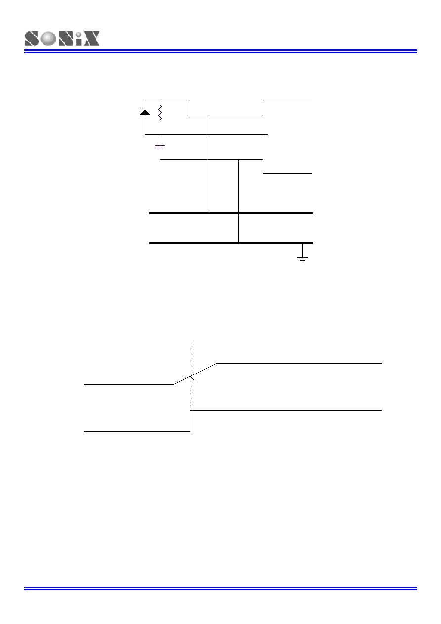
EXTERNAL RESET DESCRIPTION
The external reset is a low level active device. The reset pin receives the low voltage and resets the system. When the
voltage detects high level, it stops resetting the system. Users can use an external reset circuit to control system
operation.
External Reset
VDD
Internal Reset Signal
External Reset Detect Level
End of External Reset
System Reset
Users must make sure the VDD is stable earlier than external reset. Otherwise, the power on reset maybe fail.
The external reset circuit is a simple RC circuit as the following figure.
GND
VCC
RST
VDD
MCU
VSS
R
20K ohm
C
0.1uF
SN8P1602B
8-Bit Micro-Controller
SONiX TECHNOLOGY CO., LTD
Page 37
Version 1.1
Under different environment, by placing a diode in between VCC and reset pin will help the Brownout reset.
GND
VCC
RST
VDD
MCU
VSS
R
20K ohm
C
0.1uF
DIODE
LOW VOLTAGE DETECTOR (LVD) DESCRIPTION
The LVD is a low voltage detector. It detects VDD level and reset the system as the VDD lower than the detected
voltage. The detect level is 1.8V. If the VDD lower than 1.8V, the system resets.
System Reset
LVD Detect Level
End of LVD Reset
VDD
LVD
SN8P1602B
8-Bit Micro-Controller
SONiX TECHNOLOGY CO., LTD
Page 38
Version 1.1
7
7
7
OSCILLATORS
OVERVIEW
The SN8P1602B is a dual clock micro-controller system. There are external high-speed clock and internal low-speed
clock. The high-speed clock is generated from the external oscillator circuit. The low-speed clock is generated from
on-chip RC oscillator circuit.
Both the external high-speed clock and the internal low-speed clock can be system clock (Fosc). The system clock is
divided by 4 to be the instruction cycle (Fcpu).
Fcpu = Fosc / 4
CLOCK BLOCK DIAGRAM
fl
CPUM0
LXOSC.
fcpu
fosc/4
CPUM0
fh
HXOSC.
XIN
XOUT
STPHX
HXRC
CPUM0
Divided by 4
CLKMD
Divided by 2
OSG
Divided by 2
1 : Disable
0 : Enable
OSG : Oscillator Safe Guard
1 : Disable -- System Default
0 : Enable
HXRC(1:0) is code option
∑00= RC
∑01 =32 Khz Oscillator
∑10 = High Speed Oscillator (>10Mhz)
∑11 = Standard Oscillator (4Mhz)
fl
CPUM0
LXOSC.
fl
CPUM0
LXOSC.
fcpu
fosc/4
CPUM0
fcpu
fosc/4
CPUM0
fh
HXOSC.
XIN
XOUT
STPHX
HXRC
CPUM0
fh
HXOSC.
XIN
XOUT
STPHX
HXRC
CPUM0
Divided by 4
CLKMD
Divided by 4
Divided by 4
CLKMD
Divided by 2
Divided by 2
OSG
OSG
Divided by 2
1 : Disable
0 : Enable
OSG : Oscillator Safe Guard
1 : Disable -- System Default
0 : Enable
HXRC(1:0) is code option
∑00= RC
∑01 =32 Khz Oscillator
∑10 = High Speed Oscillator (>10Mhz)
∑11 = Standard Oscillator (4Mhz)
HXOSC: External high-speed clock
LXOSC: Internal low-speed clock
OSG: Oscillator safe guard

SN8P1602B
8-Bit Micro-Controller
SONiX TECHNOLOGY CO., LTD
Page 39
Version 1.1
OSCM REGISTER DESCRIPTION
The OSCM register is an oscillator control register. It controls oscillator status, system mode, watchdog timer clock
rate.
0CAH
Bit 7
Bit 6
Bit 5
Bit 4
Bit 3
Bit 2
Bit 1
Bit 0
OSCM
WTCKS WDRST
0
CPUM1 CPUM0 CLKMD STPHX
0
Read/Write R/W
R/W
- R/W R/W R/W R/W -
After
reset
0 0 - 0 0 0 0 -
STPHX: External high-speed oscillator control bit. 0 = free run, 1 = stop. This bit only controls external high-speed
oscillator. If STPHX=1, the internal low-speed RC oscillator is still running.
CLKMD: System high/Low clock mode: bit 0 = normal (dual) mode, 1 = slow mode.
CPUM1, CPUM0: CPU operating mode control bit:
00 = normal
01 = sleep (power down) mode
10 = green mode
11 = reserved.
WDRST: Watchdog timer reset bit
0 = Non-reset
1 = clear the watchdog timer's counter.
Please refer to the "watchdog timer chapter" for detailed information.
WTCKS: Watchdog clock source
0 = Fcpu
1 = internal RC low clock
SN8P1602B
8-Bit Micro-Controller
SONiX TECHNOLOGY CO., LTD
Page 40
Version 1.1
EXTERNAL HIGH-SPEED OSCILLATOR
SN8P1602B can be operated in four different oscillator modes. There are external RC oscillator modes, high
crystal/resonator mode (12M code option), standard crystal/resonator mode (4M code option) and low crystal mode
(32K code option). For different application, the users can select one of suitable oscillator mode by programming code
option to generate system high-speed clock source after reset.
Example: Stop external high-speed oscillator
B0BSET
FSTPHX
; To stop external high-speed oscillator only.
Example: When entering the Power Down mode, both external high-speed oscillator and internal
low-speed oscillator will be stopped.
B0BSET
FCPUM0
; To stop external high-speed oscillator and internal low-speed
; oscillator called power down mode (sleep mode).
OSCILLATOR MODE CODE OPTION
SN8P1602B has four oscillator modes for different applications. These modes are 4M, 12M, 32K and RC. The main
purpose is to support different oscillator types and frequencies. MCU needs more current when operating at
High-speed mode than the low-speed mode. For crystals, there are three steps to select. If the oscillator is RC type, to
select "RC" and the system will divide the frequency by 2 automatically. User can select oscillator mode from code
option table before compiling. Following is the code option table.
Code Option
Oscillator Mode
Remark
00
RC mode
Output the Fcpu square wave from Xout pin.
01
32K 32768Hz
10
12M 12MHz
~
16MHz
11
4M 3.58MHz
OSCILLATOR DEVIDE BY 2 CODE OPTION
SN8P1602B has a code option to divide external clock by 2,called "High_Clk / 2". If "High_Clk / 2" is enabled, the
external clock frequency is divided by 8 for the Fcpu. Fcpu is equal to Fosc/8. If "High_Clk / 2" is disabled, the Fcpu is
equal to Fosc/4.
Note: In RC mode, "High_Clk / 2" is always enabled.
OSCILLATOR SAFE GUARD CODE OPTION
SN8P1602B builds in an oscillator safe guard (OSG) to make oscillator more stable. It is a low-pass filter circuit and
stops high frequency noise into system from external oscillator circuit. This function makes system to work better under
AC noisy conditions.

SN8P1602B
8-Bit Micro-Controller
SONiX TECHNOLOGY CO., LTD
Page 41
Version 1.1
SYSTEM OSCILLATOR CIRCUITS
MCU
XIN
VDD
XOUT
VSS
CRYSTAL
20PF
20PF
Crystal/Ceramic Oscillator
MCU
XIN
VDD
VSS
XOUT
C
R
RC Oscillator
XIN
VDD
MCU
VSS
XOUT
External Clock Input
External clock input
Note1: The external oscillator circuit must be directly from Vss pin of micro-controller.
Note2: The input source of XIN pin received from external oscillator circuit, the code option can be either
be RC type oscillator or crystal type oscillator.
Note3: In RC type oscillator code option situation, the external clock frequency is automatically divided
by 2.

SN8P1602B
8-Bit Micro-Controller
SONiX TECHNOLOGY CO., LTD
Page 42
Version 1.1
External RC Oscillator Frequency Measurement
There are two ways to get the Fosc frequency of external RC oscillator. One way is to measure the XOUT output
waveform. Moreover, the other way is to measure the external RC frequency by software instruction cycle (Fcpu).
Example: Fcpu instruction cycle of external oscillator
B0BSET
P1M.0
; Set P1.0 to be output mode for outputting Fcpu toggle signal.
@@:
B0BSET
P1.0
; Output Fcpu toggle signal in low-speed clock mode.
B0BCLR
P1.0
; Measure the Fcpu frequency by oscilloscope.
JMP
@B
Note: Do not measure the RC frequency directly from XIN, the probe impendence will affect the RC
value.
SN8P1602B
8-Bit Micro-Controller
SONiX TECHNOLOGY CO., LTD
Page 43
Version 1.1
INTERNAL LOW-SPEED OSCILLATOR
The internal low-speed oscillator is built in the micro-controller. The low-speed clock source is a RC type oscillator
circuit.
Example: Stop internal low-speed oscillator
B0BSET
FCPUM0
; To stop external high-speed oscillator and internal low-speed
; oscillator called power down mode (sleep mode).
Note: The internal low-speed clock can't be turned off individually. It is controlled by CPUM0 bit of OSCM
register.
The low-speed oscillator uses RC type oscillator circuit. The frequency is affected by the voltage and temperature of
the system. In common condition, the frequency of the RC oscillator is about 16KHz at 3V and 32KHz at 5V. The
relation between the RC frequency and voltage is as the following figure.
Internal RC vs. VDD
7.329
8.663
11.998
15.333
18.668
22.003
25.338
28.673
32.008
35.343
38.678
0
5
10
15
20
25
30
35
40
1.80
2.00
2.50
3.00
3.50
4.00
4.50
5.00
5.50
6.00
6.50
VDD (Volts)
Fintrc (KHz)
Example: Measure the internal RC frequency by instruction cycle (Fcpu). The internal RC frequency is the
Fcpu multiplied by 4. We can get the Fosc frequency of internal RC from the Fcpu frequency.
B0BSET
P1M.0
; Set P1.0 to be output mode for outputting Fcpu toggle signal.
B0BSET
FCLKMD
; Switch the system clock to internal low-speed clock mode.
@@:
B0BSET
P1.0
; Output Fcpu toggle signal in low-speed clock mode.
B0BCLR
P1.0
; Measure the Fcpu frequency by oscilloscope.
JMP
@B

SN8P1602B
8-Bit Micro-Controller
SONiX TECHNOLOGY CO., LTD
Page 44
Version 1.1
SYSTEM MODE DESCRIPTION
OVERVIEW
The chip is featured with low power consumption by switching around four different modes as following.
High-speed mode
Low-speed mode
Power-down mode (Sleep mode)
Green mode
NORMAL MODE
In normal mode, the system clock source is external high-speed clock. After power on, the system works under normal
mode. The instruction cycle is fosc/4. When the external high-speed oscillator is 3.58MHz, the instruction cycle is
3.58MHz/4 = 895KHz. From normal mode, the system can get into power down mode, slow mode and green mode.
SLOW MODE
In slow mode, the system clock source is internal low-speed RC clock. To set CLKMD =1, the system switches into
slow mode. In slow mode, the system functions similar to the normal mode except using the internal RC clock. The
system in slow mode can switch back to high-speed normal mode. On the other hand, it can be easily switch to power
down mode and green mode for less power consumption.
GREEN MODE
The green mode provides a time-variable wakeup function. Users can decide wakeup time by setting TC0 timer. There
are two paths into green mode. One is from normal mode and the other is from slow mode. In normal mode, the TC0
timer overflow time is very short. In slow mode, the overflow time is longer. Users can select appropriate situation for
their applications. Under green mode, the power consumption is around 5uA in 3V condition. The system can be
waked up to last system mode by TC0 timer timeout and P0 trigger signal.
POWER DOWN MODE
The power down mode is also called sleep mode. The MCU stops working as sleeping status. To set CUPM0 = 1, the
system gets into power down mode. The external high-speed and low-speed oscillators are turned off. The system can
be waked up by P0, P1 trigger signal.
SN8P1602B
8-Bit Micro-Controller
SONiX TECHNOLOGY CO., LTD
Page 45
Version 1.1
SYSTEM MODE CONTROL
SN8P1602B Type
Operating mode description
MODE NORMAL SLOW GREEN
POWER
DOWN
(SLEEP)
REMARK
HX osc.
Running
By STPHX
By STPHX
Stop
LX
osc. Running Running Running Stop
CPU instruction
Executing Executing
Stop
Stop
TC0 timer
*Active
*Active *Active Inactive
* Active by
program
Watchdog timer
Active
Active
By
INT_16K_RC
By
INT_16K_RC
Internal
interrupt
All active
All active
TC0
All inactive
External
interrupt
All active
All active
All active
All inactive
Wakeup source
-
-
P0, P1, TC0
Reset
P0, P1, Reset
Normal Mode
Green Mode
Slow Mode
Power Down Mode
(Sleep Mode)
P0, P1 wake-up function active.
External reset circuit active.
CPUM1, CPUM0 = 01
CLKMD = 0
CLKMD = 1
CPUM1, CPUM0 = 10
P0, P1 wake-up function active.
TC0 time out.
P0, P1 wake-up function active.
TC0 time out.
External reset circuit active.
External reset circuit active.

SN8P1602B
8-Bit Micro-Controller
SONiX TECHNOLOGY CO., LTD
Page 46
Version 1.1
SYSTEM MODE SWITCHING
Switch normal/slow mode to power down (sleep) mode.
CPUM0 = 1
B0BSET
FCPUM0
; Set CPUM0 = 1.
During the sleep, only the wakeup pin and reset can wakeup the system back to the normal mode.
Switch normal mode to slow mode.
B0BSET
FCLKMD
;To set CLKMD = 1, Change the system into slow mode
B0BSET
FSTPHX
;To stop external high-speed oscillator for power saving.
Switch slow mode to normal mode (The external high-speed oscillator is still running)
B0BCLR
FCLKMD
;To set CLKMD = 0
Switch slow mode to normal mode (The external high-speed oscillator stops)
If external high clock stop and program want to switch back normal mode. It is necessary to delay at least 10mS for
external clock stable.
B0BCLR
FSTPHX
; Turn on the external high-speed oscillator.
B0MOV
Z, #27
; If VDD = 5V, internal RC=32KHz (typical) will delay
@@:
DECMS
Z
; 0.125ms X 81 = 10.125ms for external clock stable
JMP
@B
;
B0BCLR
FCLKMD
; Change the system back to the normal mode
Example: Go into Green mode and enable TC0 wakeup function.
; Set TC0 timer wakeup function.
B0BCLR
FTC0IEN
; To disable TC0 interrupt service
B0BCLR
FTC0ENB
; To disable TC0 timer
MOV
A,#20H
;
B0MOV
TC0M,A
; To set TC0 clock = Fcpu / 64
MOV
A,#74H
B0MOV
TC0C,A
; To set TC0C initial value = 74H (To set TC0 interval = 10
ms)
B0BCLR
FTC0IEN
; To disable TC0 interrupt service
B0BCLR
FTC0IRQ
; To clear TC0 interrupt request
B0BSET
FTC0ENB
; To enable TC0 timer
B0BSET
FTC0GN
; To enable TC0 wakeup function
; Go into green mode
B0BCLR
FCPUM0
;To set CPUMx = 10
B0BSET
FCPUM1
Note: If TC0ENB = 0 or TC0GN = 0, TC0 will not be able to wakeup from green mode to normal/slow mode
function.
SN8P1602B
8-Bit Micro-Controller
SONiX TECHNOLOGY CO., LTD
Page 47
Version 1.1
WAKEUP TIME
OVERVIEW
The external high-speed oscillator needs a delay time from stopping to operating. The delay is necessary for oscillator
to be stabilized.. The delay time for external high-speed oscillator restart is sometimes called wakeup time.
Following are two conditions require wakeup time, one is switching power down mode to normal mode, and the other is
switching slow mode to normal mode. For the first condition, SN8P1602B provides 2048 oscillator clocks as the
wakeup time. The second condition, users need to take the wakeup time into consideration, which involved stabilizing
period for start up the external high-speed oscillator.
HARDWARE WAKEUP
When the system is in power down mode (sleep mode), the external high-speed oscillator stops. When waked up from
power down mode, MCU waits for 2048 external high-speed oscillator clocks as the wakeup time to stable the oscillator
circuit. After the wakeup time, the system goes into the normal mode. The value of the wakeup time is as the following.
The Wakeup time = 1/Fosc * 2048 (sec) + X'tal settling time
The X'tal settling time is depended on the X'tal type. Typically, it is about 2~4mS.
Example: In power down mode (sleep mode), the system is waked up by P0 or P1 trigger signal. After the
wakeup time, the system goes into normal mode. The wakeup time of P0, P1 wakeup function is as the
following.
The wakeup time = 1/Fosc * 2048 = 0.57 ms
(Fosc = 3.58MHz)
The total wakeup time = 0.57ms + X'tal settling time
Under power down mode (sleep mode), only the I/O ports with wakeup function are able to wake the system up to
normal mode. The Port 0 and Port 1 have wakeup function. Port 0 wakeup function always enables, but the Port 1 is
controlled by the P1W register.
SN8P1602B
0C0H
Bit 7
Bit 6
Bit 5
Bit 4
Bit 3
Bit 2
Bit 1
Bit 0
P1W
0
0
0 P14W P13W P12W P11W P10W
Read/Write
-
-
- R/W R/W R/W R/W R/W
After
reset
- - - 0 0 0 0 0
P10W~P14W: Port 1 wakeup function control bits. 0 = none wakeup function, 1 = Enable each pin of Port 1 wakeup
function.

SN8P1602B
8-Bit Micro-Controller
SONiX TECHNOLOGY CO., LTD
Page 48
Version 1.1
EXTERNAL WAKEUP TRIGGER CONTROL
In the SN8P1602B, the wakeup trigger direction is control by PEDGE register.
PEDGE initial value = 0xx0 0xxx
0BFH
Bit 7
Bit 6
Bit 5
Bit 4
Bit 3
Bit 2
Bit 1
Bit 0
PEDGE
PEDGEN
-
- P00G1
P00G0 -
-
-
R/W
- -
R/W
R/W
- - -
Bit7
PEDGEN: Interrupt and wakeup trigger edge control bit.
0 = Disable edge trigger function.
Port 0: Low-level wakeup trigger and falling edge interrupt trigger.
Port 1: Low-level wakeup trigger.
1 = Enable edge trigger function.
P0.0: Wakeup and interrupt trigger is controlled by P00G1 and P00G0 bits.
Port 1: Level change (falling or rising edge) wakeup trigger.
Bit[4:3]
P00G[1:0]: Port 0.0 edge select bits.
00 = reserved,
01 = rising edge,
10 = falling edge,
11 = rising/falling bi-direction.

SN8P1602B
8-Bit Micro-Controller
SONiX TECHNOLOGY CO., LTD
Page 49
Version 1.1
8
8
8
TIMERS
WATCHDOG TIMER (WDT)
The watchdog timer (WDT) is a binary up counter designed for monitoring program execution. If the program goes into
the unknown status by noise interference, WDT overflow signal raises and resets MCU. The instruction that clears the
watchdog timer (" B0BSET FWDRST ") should be executed within a certain period. If an instruction that clears the
watchdog timer is not executed within the period and the watchdog timer overflows, reset signal is generated and
system is restarted.
0CAH
Bit 7
Bit 6
Bit 5
Bit 4
Bit 3
Bit 2
Bit 1
Bit 0
OSCM
WTCKS WDRST
0
CPUM1 CPUM0 CLKMD STPHX
0
Read/Write R/W
R/W
- R/W R/W R/W R/W -
After
reset
0 0 - 0 0 0 0 -
WDRST: Watchdog timer reset bit. 0 = Non reset, 1 = clear the watchdog timer counter.
WTCKS: Watchdog clock source select bit 0 = Fcpu, 1 = internal RC low clock.
Watchdog timer overflow table.
WTCKS
CLKMD
Code Option
Watchdog Timer Overflow Time
0
0
4M_X'tal / 12M_X'tal / RC
1 / ( Fcpu
˜
2
14
˜
16 ) = 293 ms, Fosc=3.58MHz
0 0
32K_X'tal
1 / ( Fcpu
˜
2
8
˜
16 ) = 500 ms, Fosc=32768Hz
0 1
-
1 / ( Fcpu
˜
2
14
˜
16 ) = 65.5s, Fosc=16KHz@3V
1 -
-
1 / ( 16K
˜
512
˜
16 ) ~ 0.5s @3V
- - Enable
Int_16K_RC
1 / ( 16K
˜
512
˜
16 ) ~ 0.5s @3V
Note: The watchdog timer can be enabled or disabled by the code option. If disabled, the watchdog
timer can also be served as fixed-period timer by checking the NT0 flag.
Example: An operation of watchdog timer is as following. To clear the watchdog timer counter in the top
of the main routine of the program.
Main:
B0BSET
FWDRST
; Clear the watchdog timer counter.
. .
CALL
SUB1
CALL
SUB2
. .
. .
. .
JMP
MAIN

SN8P1602B
8-Bit Micro-Controller
SONiX TECHNOLOGY CO., LTD
Page 50
Version 1.1
TIMER0 (TC0)
OVERVIEW
The TC0 is an 8-bit binary up timer and event counter,
using TC0M register to select TC0C's clock source from GTMR
or from external INT0 pin ( falling edge trigger) for counting a precision time. If TC0 timer occurs an overflow (from FFH
to 00H), it will continue counting and issue a time-out signal to trigger TC0 interrupt to request interrupt service.
The main purposes of the TC0 timer is as following.
8-bit programmable timer: Generates interrupts at specific time intervals based on the selected clock
frequency.
External event counter: Counts system "events" based on falling edge detection of external clock signals at
the INT0 input pin.
˜
2
(8
-TC0Rate
)
Fcpu
TC0enb
TC0C
8-bit b inary counter
TC0 Time out
pre_load
INT0
(schmitter trigger)
TC0cks
Internal data bus
CPUM1,0
˜
2
(8
-TC0Rate
)
Fcpu
TC0enb
TC0C
8-bit b inary counter
TC0 Time out
pre_load
INT0
(schmitter trigger)
TC0cks
Internal data bus
CPUM1,0

SN8P1602B
8-Bit Micro-Controller
SONiX TECHNOLOGY CO., LTD
Page 51
Version 1.1
TC0M MODE REGISTER
The TC0M is an 8-bit read/write timer mode register. By loading different value into the TC0M register, users can
modify the timer period as program executing.
Eight rates for TC0 timer can be selected by TC0RATE0 ~ TC0RATE2 bits. The range is from fcpu/2 to fcpu/256. The
TC0M initial value is zero and the rate is fcpu/256. The bit7 of TC0M called TC0ENB is the control bit to start TC0 timer.
The combination of these bits is to determine the TC0 timer clock frequency and the intervals.
0DAH
Bit 7
Bit 6
Bit 5
Bit 4
Bit 3
Bit 2
Bit 1
Bit 0
TC0M
TC0ENB TC0rate2 TC0rate1
TC0rate0
TC0CKS
0
0
0
Read/Write
R/W R/W R/W R/W R/W -
-
-
After
reset
0 0 0 0 0 - - -
TC0ENB: TC0 counter enable bit. "0" = disable, "1" = enable.
TC0RATE2~TC0RATE0: TC0 internal clock select bits. 000 = fcpu/256, 001 = fcpu/128, ... , 110 = fcpu/4, 111 =
fcpu/2.
TC0CKS: TC0 clock source select bit. 0 = Fcpu, 1 = External clock comes from INT0/P0.0 pin.
Note1: The ICE S8KC does not support the PWM0OUT and TC0OUT Function. The PWM0OUT and
TC0OUT must use the S8KD ICE (or later) to verify the function.
Note2: When TC0CKS=1, TC0 became an external event counter. No more P0.0 interrupt request will be
raised. (P0.0IRQ will be always 0)
SN8P1602B
8-Bit Micro-Controller
SONiX TECHNOLOGY CO., LTD
Page 52
Version 1.1
TC0C COUNTING REGISTER
TC0C is an 8-bit counter register for the timer (TC0). TC0C must be reset whenever the TC0ENB is set to "1" to start
the timer. TC0C is incremented each time a clock pulse of the frequency determined by TC0RATE0 ~ TC0RATE2.
When TC0C has incremented to "0FFH", it counts to "00H" an overflow generated. Under TC0 interrupt service request
(TC0IEN) enable condition, the TC0 interrupt request flag will be set to "1" and the system executes the interrupt
service routine. The TC0C has no auto reload function. After TC0C overflow, the TC0C is continuing counting. Users
need to redefine the TC0C value to get an accurate time.
0DBH
Bit 7
Bit 6
Bit 5
Bit 4
Bit 3
Bit 2
Bit 1
Bit 0
TC0C
TC0C7 TC0C6 TC0C5 TC0C4 TC0C3 TC0C2 TC0C1 TC0C0
Read/Write R/W
R/W
R/W R/W R/W R/W R/W R/W
After
reset
0 0 0 0 0 0 0 0
The basic timer table interval time of TC0
High speed mode (Fcpu = 3.58MHz / 4)
Low speed mode (Fcpu = 32768Hz / 4)
TC0RATE TC0CLOCK
Max overflow interval One step = max/256
Max overflow interval One step = max/256
000
fcpu/256
73.2 ms
286us
8000 ms
31.25 ms
001
fcpu/128
36.6 ms
143us
4000 ms
15.63 ms
010
fcpu/64
18.3 ms
71.5us
2000 ms
7.8 ms
011
fcpu/32
9.15 ms
35.8us
1000 ms
3.9 ms
100
fcpu/16
4.57 ms
17.9us
500 ms
1.95 ms
101
fcpu/8
2.28 ms
8.94us
250 ms
0.98 ms
110
fcpu/4
1.14 ms
4.47us
125 ms
0.49 ms
111
fcpu/2
0.57 ms
2.23us
62.5 ms
0.24 ms
The equation of TC0C initial value is as following.
TC0C initial value = 256 - (TC0 interrupt interval time * input clock)
Example: To set 10ms interval time for TC0 interrupt at 3.58MHz high-speed mode. TC0C value (74H) =
256 - (10ms * fcpu/64)
TC0C initial value = 256 - (TC0 interrupt interval time * input clock)
= 256 - (10ms * 3.58 * 10
6
/ 4 / 64)
= 256 - (10
-2
* 3.58 * 10
6
/ 4 / 64)
= 116
= 74H

SN8P1602B
8-Bit Micro-Controller
SONiX TECHNOLOGY CO., LTD
Page 53
Version 1.1
TC0 TIMER OPERATION SEQUENCE
The TC0 timer's sequence of operation may be as following.
Set the TC0C initial value to setup the interval time.
Set the TC0ENB to be "1" to enable TC0 timer.
TC0C is incremented by one after each clock pulse corresponding to TC0M selection.
TC0C overflow if TC0C from FFH to 00H.
When TC0C overflow occur, the TC0IRQ flag is set to be "1" by hardware.
Execute the interrupt service routine.
Users reset the TC0C value and resume the TC0 timer operation.
Example: Setup the TC0M and TC0C.
B0BCLR
FTC0IEN
; To disable TC0 interrupt service
B0BCLR
FTC0ENB
; To disable TC0 timer
MOV
A,#20H
;
B0MOV
TC0M,A
; To set TC0 clock = Fcpu / 64
MOV
A,#74H
; To set TC0C initial value = 74H
B0MOV
TC0C,A
;(To
set
TC0 interval = 10 ms)
B0BSET
FTC0IEN
; To enable TC0 interrupt service
B0BCLR
FTC0IRQ
; To clear TC0 interrupt request
B0BSET
FTC0ENB
; To enable TC0 timer
Example: TC0 interrupt service routine.
ORG
8
; Interrupt vector
JMP
INT_SERVICE
INT_SERVICE:
B0XCH
A, ACCBUF
; B0xch instruction do not change C,Z flag
B0MOV
A,
PFLAG
B0MOV
PFLAGBUF,
A
B0BTS1
FTC0IRQ
; Check TC0IRQ
JMP
EXIT_INT
; TC0IRQ = 0, exit interrupt vector
B0BCLR
FTC0IRQ
; Reset TC0IRQ
MOV
A,#74H
; Reload TC0C
B0MOV
TC0C,A
.
.
; TC0 interrupt service routine
. .
JMP
EXIT_INT
; End of TC0 interrupt service routine and exit interrupt
vector
. .
. .
EXIT_INT:
B0MOV
A,
PFLAGBUF
B0MOV
PFLAG,
A
B0XCH
A, ACCBUF
; Restore ACC value.
RETI
; Exit interrupt vector

SN8P1602B
8-Bit Micro-Controller
SONiX TECHNOLOGY CO., LTD
Page 54
Version 1.1
9
9
9
INTERRUPT
OVERVIEW
The SN8P1602B provides 2 interrupt sources, including 1 internal interrupt (TC0) and 1 external interrupt (INT0). The
external interrupt can wakeup the chip while the system is switched from power down mode to high-speed normal
mode. Once interrupt service is executed, the GIE bit in STKP register will clear to "0" for stopping other interrupt
request. On the contrast, when interrupt service exits, the GIE bit will set to "1" to accept the next interrupts' request. All
of the interrupt request signals are stored in INTRQ register.
SN8P1602B
Note: The GIE bit must enable during all interrupt operation.
INTRQ
2-bit
Latchs
TC0IRQ
Interrupt
enable
gating
Global interrupt request signal
Interrupt vector address (0008H)
TC0 time out
INTEN Interrupt enable register
The interrupt trigger edge :
INT0 = falling edge
P00IRQ
INT0 trigger
INTRQ
2-bit
Latchs
TC0IRQ
Interrupt
enable
gating
Global interrupt request signal
Interrupt vector address (0008H)
TC0 time out
INTEN Interrupt enable register
The interrupt trigger edge :
INT0 = falling edge
P00IRQ
INT0 trigger
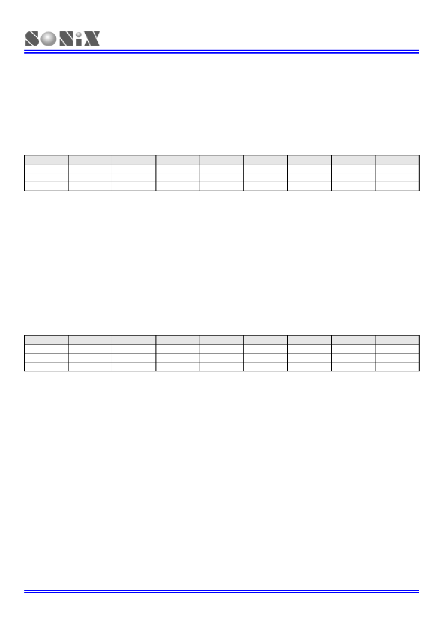
SN8P1602B
8-Bit Micro-Controller
SONiX TECHNOLOGY CO., LTD
Page 55
Version 1.1
INTEN INTERRUPT ENABLE REGISTER
INTEN is the interrupt request control register including one internal interrupts, one external interrupts enable control
bits. One of the register to be set "1" is to enable the interrupt request function. Once of the interrupt occur, the stack is
incremented and program jump to ORG 8 to execute interrupt service routines. The program exits the interrupt service
routine when the returning interrupt service routine instruction (RETI) is executed.
SN8P1602B
0C9H
Bit 7
Bit 6
Bit 5
Bit 4
Bit 3
Bit 2
Bit 1
Bit 0
INTEN
0 0
TC0IEN
0 0 0 0
P00IEN
Read/Write
- -
R/W
- - - -
R/W
After
reset
- - 0 - - - - 0
P00IEN : External P0.0 interrupt control bit. 0 = disable, 1 = enable.
TC0IEN : Timer 0 interrupt control bit 0 = disable, 1 = enable.
INTRQ INTERRUPT REQUEST REGISTER
INTRQ is the interrupt request flag register. The register includes all interrupt request indication flags. Each one of the
interrupt requests occurs, the bit of the INTRQ register would be set "1". The INTRQ value needs to be clear by
programming after detecting the flag. In the interrupt vector of program, users know the any interrupt requests
occurring by the register and do the routine corresponding of the interrupt request.
SN8P1602B
0C8H
Bit 7
Bit 6
Bit 5
Bit 4
Bit 3
Bit 2
Bit 1
Bit 0
INTRQ
0 0
TC0IRQ
0 0 0 0
P00IRQ
Read/Write
- -
R/W
- - - -
R/W
After
reset
- - 0 - - - - 0
P00IRQ : External P0.0 interrupt request bit. 0 = non-request, 1 = request.
TC0IRQ : TC0 timer interrupt request controls bit 0 = non request, 1 = request.
When interrupt occurs, the related request bit of INTRQ register will be set to "1" no matter the related enable bit of
INTEN register is enabled or disabled. If the related bit of INTEN = 1 and the related bit of INTRQ is also set to be "1".
As the result, the system will execute the interrupt vector (ORG 8). If the related bit of INTEN = 0, moreover, the
system won't execute interrupt vector even when the related bit of INTRQ is set to be "1". Users need to be cautious
with the operation under multi-interrupt situation.
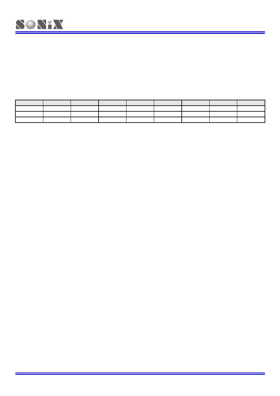
SN8P1602B
8-Bit Micro-Controller
SONiX TECHNOLOGY CO., LTD
Page 56
Version 1.1
INTERRUPT OPERATION DESCRIPTION
GIE GLOBAL INTERRUPT OPERATION
GIE is the global interrupt control bit. All interrupts start work after the GIE = 1. It is necessary for interrupt service
request. One of the interrupt requests occurs, and the program counter (PC) points to the interrupt vector (ORG 8) and
the stack add 1 level.
SN8P1602B
0DFH
Bit 7
Bit 6
Bit 5
Bit 4
Bit 3
Bit 2
Bit 1
Bit 0
STKP
GIE
- - - -
STKPB2
STKPB1
STKPB0
Read/Write
R/W
- - - -
R/W
R/W
R/W
After
reset
0 - - - - 1 1 1
GIE: Global interrupt control bit. 0 = disable, 1 = enable.
Example: Set global interrupt control bit (GIE).
B0BSET
FGIE
; Enable GIE
Note: The GIE bit must enable during all interrupt operation.

SN8P1602B
8-Bit Micro-Controller
SONiX TECHNOLOGY CO., LTD
Page 57
Version 1.1
INT0 (P0.0) INTERRUPT OPERATION
The P0.0 interrupt trigger direction is control by PEDGE register.
PEDGE initial value = 0xx0 0xxx
0BFH
Bit 7
Bit 6
Bit 5
Bit 4
Bit 3
Bit 2
Bit 1
Bit 0
PEDGE
PEDGEN
-
- P00G1
P00G0 -
-
-
R/W
- -
R/W
R/W
- - -
Bit7
PEDGEN: Interrupt and wakeup trigger edge control bit.
0 = Disable edge trigger function.
Port 0: Low-level wakeup trigger and falling edge interrupt trigger.
Port 1: Low-level wakeup trigger.
1 = Enable edge trigger function.
P0.0: Wakeup and interrupt trigger is controlled by P00G1 and P00G0 bits.
Port 1: Level change (falling or rising edge) wakeup trigger.
Bit[4:3]
P00G[1:0]: Port 0.0 edge select bits.
00 = reserved,
01 = rising edge,
10 = falling edge,
11 = rising/falling bi-direction.
Example: INT0 interrupt request setup.
B0BSET
FP00IEN
;
Enable
INT0 interrupt service
B0BCLR
FP00IRQ
; Clear INT0 interrupt request flag
B0BSET
FGIE
; Enable GIE
Example: INT0 interrupt service routine.
ORG
8
; Interrupt vector
JMP
INT_SERVICE
INT_SERVICE:
B0XCH
A, ACCBUF
; Store ACC value.
B0MOV
A,
PFLAG
B0MOV
PFLAGBUF,
A
B0BTS1
FP00IRQ
; Check P00IRQ
JMP
EXIT_INT
; P00IRQ = 0, exit interrupt vector
B0BCLR
FP00IRQ
; Reset P00IRQ
.
.
; INT0 interrupt service routine
. .
EXIT_INT:
B0MOV
A,
PFLAGBUF
B0MOV
PFLAG,
A
B0XCH
A, ACCBUF
; Restore ACC value.
RETI
; Exit interrupt vector
When the INT0 trigger occurs, the P00IRQ will be set to "1" no matter the P00IEN is enable or disable. If the P00IEN =
1 and the trigger event P00IRQ is also set to be "1". As the result, the system will execute the interrupt vector (ORG
8). If the P00IEN = 0 and the trigger event P00IRQ is still set to be "1". Moreover, the system won't execute interrupt
vector even when the P00IRQ is set to be "1". Users need to be cautious with the operation under multi-interrupt
situation.

SN8P1602B
8-Bit Micro-Controller
SONiX TECHNOLOGY CO., LTD
Page 58
Version 1.1
TC0 INTERRUPT OPERATION
Example: TC0 interrupt request setup.
B0BCLR
FTC0IEN
; Disable TC0 interrupt service
B0BCLR
FTC0ENB
; Disable TC0 timer
MOV
A,
#20H
;
B0MOV
TC0M, A
; Set TC0 clock = Fcpu / 64
MOV
A, #74H
; Set TC0C initial value = 74H
B0MOV
TC0C, A
; Set TC0 interval = 10 ms
B0BSET
FTC0IEN
; Enable TC0 interrupt service
B0BCLR
FTC0IRQ
; Clear TC0 interrupt request flag
B0BSET
FTC0ENB
; Enable TC0 timer
B0BSET
FGIE
; Enable GIE
Example: TC0 interrupt service routine.
ORG
8
; Interrupt vector
JMP
INT_SERVICE
INT_SERVICE:
B0XCH
A, ACCBUF
; Store ACC value.
B0MOV
A,
PFLAG
B0MOV
PFLAGBUF,
A
B0BTS1
FTC0IRQ
; Check TC0IRQ
JMP
EXIT_INT
; TC0IRQ = 0, exit interrupt vector
B0BCLR
FTC0IRQ
; Reset TC0IRQ
MOV
A,
#74H
B0MOV
TC0C, A
; Reset TC0C.
.
.
; TC0 interrupt service routine
. .
EXIT_INT:
B0MOV
A,
PFLAGBUF
B0MOV
PFLAG,
A
B0XCH
A, ACCBUF
; Restore ACC value.
RETI
; Exit interrupt vector
When the TC0C counter overflows, the TC0IRQ will be set to "1" no matter the TC0IEN is enable or disable. If the
TC0IEN and the trigger event TC0IRQ is set to be "1". As the result, the system will execute the interrupt vector. If the
TC0IEN = 0, the trigger event TC0IRQ is still set to be "1". Moreover, the system won't execute interrupt vector even
when the TC0IEN is set to be "1". Users need to be cautious with the operation under multi-interrupt situation.

SN8P1602B
8-Bit Micro-Controller
SONiX TECHNOLOGY CO., LTD
Page 59
Version 1.1
MULTI-INTERRUPT OPERATION
Under certain condition, the software designer uses more than one interrupt requests. Processing multi-interrupt
request requires setting the priority of the interrupt requests. The IRQ flags of interrupts are controlled by the interrupt
event. Nevertheless, the IRQ flag "1" doesn't mean the system will execute the interrupt vector. And which means the
IRQ flags can be set "1" by the events without enable the interrupt. Once the event occurs, the IRQ will be logic "1".
The IRQ and its trigger event relationship is as the below table.
Interrupt Name
Trigger Event Description
P00IRQ
P0.0 trigger controlled by PEDGE
TC0IRQ TC0C
overflow
For multi-interrupt conditions, two things need to be taking care of. One is to set the priority for these interrupt requests.
Two is using IEN and IRQ flags to decide which interrupt to be executed. Users have to check interrupt control bit and
interrupt request flag in interrupt routine.
Example: Check the interrupt request under multi-interrupt operation
ORG
8
; Interrupt vector
B0XCH
A, ACCBUF
; Store ACC value.
B0MOV
A, PFLAG
; Store PFLAG value
B0MOV
PFLAGBUF,A
INTP00CHK:
; Check INT0 interrupt request
B0BTS1
FP00IEN
; Check P00IEN
JMP
INTTC0CHK
; Jump check to next interrupt
B0BTS0
FP00IRQ
; Check P00IRQ
JMP
INTP00
; Jump to INT0 interrupt service routine
INTTC0CHK:
; Check TC0 interrupt request
B0BTS1
FTC0IEN
; Check TC0IEN
JMP
INT_EXIT
; Jump to exit of IRQ
B0BTS0
FTC0IRQ
; Check TC0IRQ
JMP
INTTC0
; Jump to TC0 interrupt service routine
INT_EXIT:
B0MOV
A, PFLAGBUF
; Restore PFLAG value
B0MOV
PFLAG,A
B0XCH
A, ACCBUF
; Restore ACC value.
RETI
; Exit interrupt vector

SN8P1602B
8-Bit Micro-Controller
SONiX TECHNOLOGY CO., LTD
Page 60
Version 1.1
1
1
1
0
0
0
I/O PORT
OVERVIEW
The SN8P1602B provides 3 ports for users' application, consisting one input only port (P0) and two I/O ports (P1, P2,).
Each port consists input pull-up resistors. The direction of I/O port can be selected by PnM register. When the system
resets, these ports will then be set as input port without pull up resistors.
The pull-up resistor can be set up by PUR register.
SN8P1602B
Note: All of the latch output circuits are push-pull structures.
.
Port0 structure
PUR
PUR
PUR
PnM, PUR
Pin
PnM
Latch
Port1~Port2 structure
PnM
Pin
Int. bus
Port0 structure
PUR
PUR
PUR
PnM, PUR
Pin
PnM
Latch
Port1~Port2 structure
PnM
Pin
Int. bus
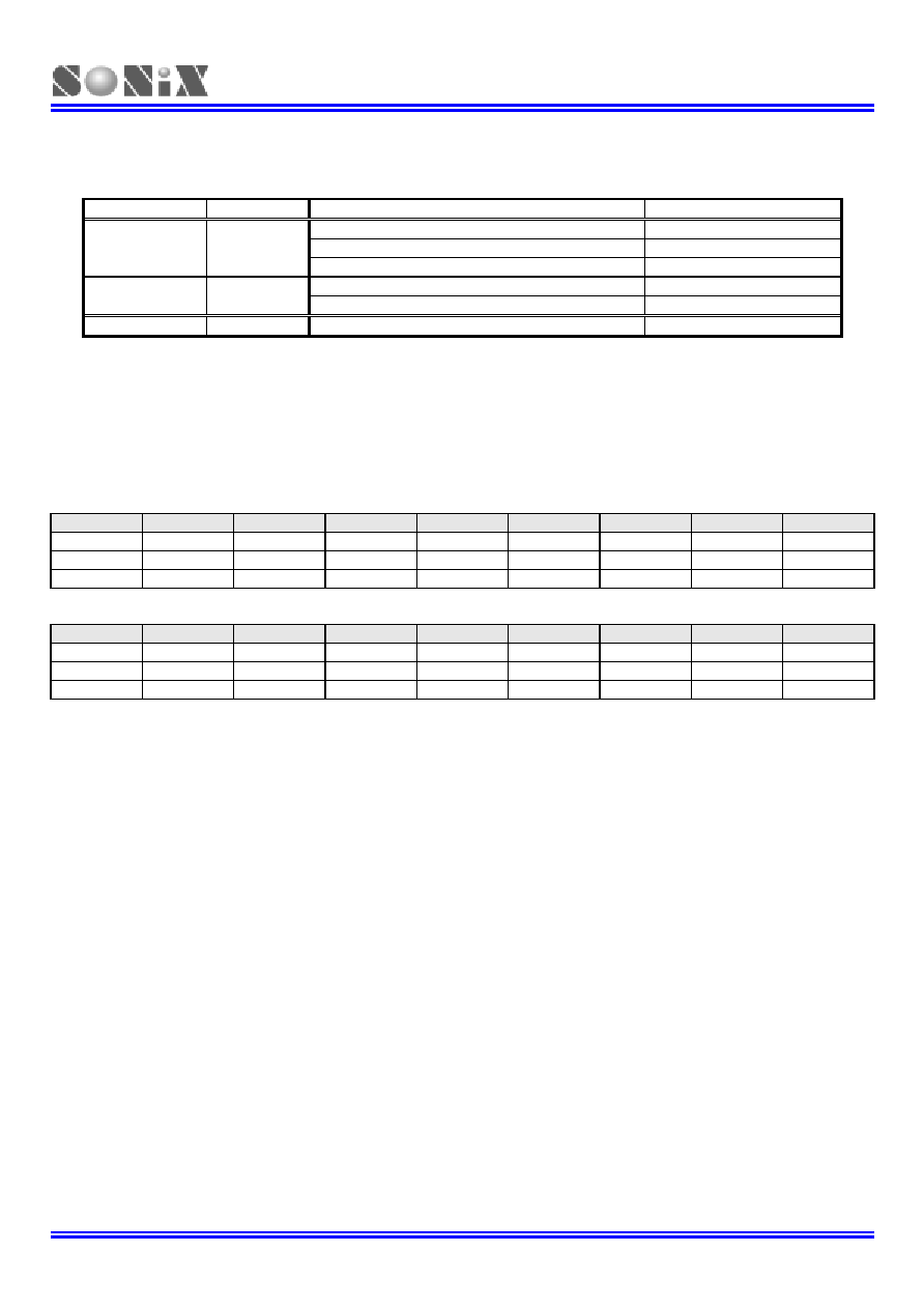
SN8P1602B
8-Bit Micro-Controller
SONiX TECHNOLOGY CO., LTD
Page 61
Version 1.1
I/O PORT FUNCTION TABLE
SN8P1602B
Port/Pin I/O
Function
Description
Remark
General-purpose input function
External interrupt (INT0)
See <P00G1,P00G0>
P0.0 I
Wakeup from power down mode
See <P00G1,P00G0>
General-purpose input/output function
P1.0~P1.4 I/O
Wakeup from power down mode
Level Change
P2.0~P2.7
I/O
General-purpose input/output function
Note: The P1.4 enables when the external oscillator is RC type.
I/O PORT MODE
The port direction is programmed by PnM register. Port 0 is always input mode. Port 1 and Port 2 can select input or
output direction.
SN8P1602B
0C1H
Bit 7
Bit 6
Bit 5
Bit 4
Bit 3
Bit 2
Bit 1
Bit 0
P1M
0
0
0 P14M P13M P12M P11M P10M
Read/Write
-
-
- R/W R/W R/W R/W R/W
After
reset
- - - 0 0 0 0 0
SN8P1602B
0C2H
Bit 7
Bit 6
Bit 5
Bit 4
Bit 3
Bit 2
Bit 1
Bit 0
P2M
P27M P26M P25M P24M P23M P22M P21M P20M
Read/Write R/W
R/W
R/W R/W R/W R/W R/W R/W
After
reset
0 0 0 0 0 0 0 0
When PnM=0, the Pn is input mode
PnM=1, the Pn is output mode
Users can program them by bit control instructions (B0BSET, B0BCLR).
Example: I/O mode selecting
CLR
P1M
; Set all ports to be input mode.
CLR
P2M
MOV
A, #0FFH
; Set all ports to be output mode.
B0MOV
P1M,
A
B0MOV
P2M,
A
B0BCLR
P1M.2
; Set P1.2 to be input mode.
B0BSET
P1M.2
; Set P1.2 to be output mode.
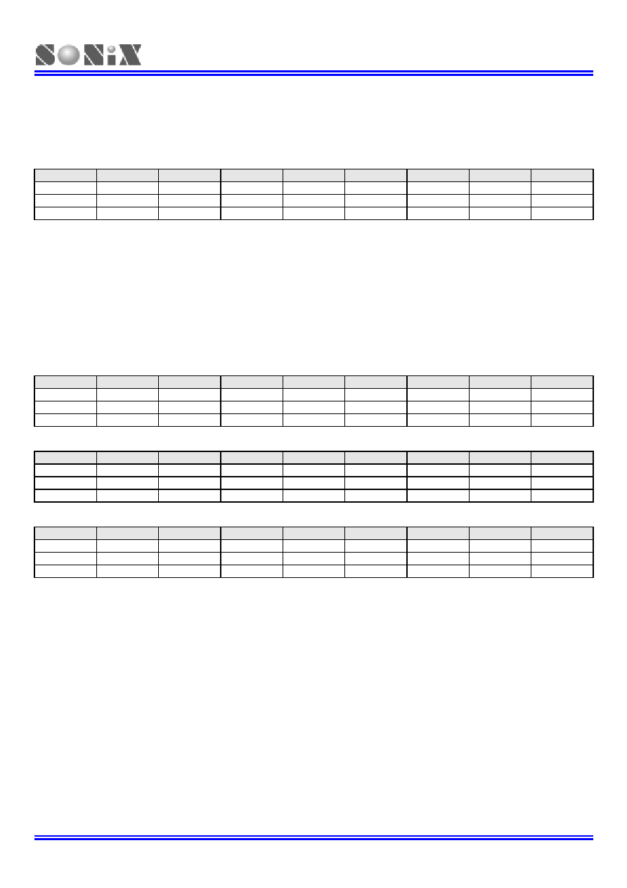
SN8P1602B
8-Bit Micro-Controller
SONiX TECHNOLOGY CO., LTD
Page 62
Version 1.1
I/O PULL UP REGISTER
SN8P1602B
0BEH
Bit 7
Bit 6
Bit 5
Bit 4
Bit 3
Bit 2
Bit 1
Bit 0
PUR
- - - - -
PUR2
PUR1
PUR0
Read/Write
- - - - - W
W
W
After
reset
- - - - - 0 0 0
Example: I/O Pull up Register
CLR
PUR
; Disable all ports Pull-up register.
MOV
A, #07H
; Enable Port0, 1, 2 Pull-up register,
B0MOV
PUR,
A
;
I/O PORT DATA REGISTER
SN8P1602B
0D0H
Bit 7
Bit 6
Bit 5
Bit 4
Bit 3
Bit 2
Bit 1
Bit 0
P0
- - - - - - -
P00
Read/Write
- - - - - - - R
After
reset
- - - - - - - 0
SN8P1602B
0D1H
Bit 7
Bit 6
Bit 5
Bit 4
Bit 3
Bit 2
Bit 1
Bit 0
P1
-
-
- P14 P13 P12 P11 P10
Read/Write
-
-
- R/W R/W R/W R/W R/W
After
reset
- - - 0 0 0 0 0
SN8P1602B
0D2H
Bit 7
Bit 6
Bit 5
Bit 4
Bit 3
Bit 2
Bit 1
Bit 0
P2
P27 P26 P25 P24 P23 P22 P21 P20
Read/Write R/W
R/W
R/W R/W R/W R/W R/W R/W
After
reset
0 0 0 0 0 0 0 0
Example: Read data from input port.
B0MOV
A, P0
; Read data from Port 0
B0MOV
A, P1
; Read data from Port 1
B0MOV
A, P2
; Read data from Port 2
Example: Write data to output port.
MOV
A, #55H
; Write data 55H to Port 1 and Port 2
B0MOV
P1,
A
B0MOV
P2,
A
Example: Write one bit data to output port.
B0BSET
P1.3
; Set P1.3 and P2.5 to be "1".
B0BSET
P2.5
B0BCLR
P1.3
; Set P1.3 and P2.5 to be "0".
B0BCLR
P2.5
Example: Port bit test.
B0BTS1
P0.0
; Bit test 1 for P0.0
B0BTS0
P1.2
; Bit test 0 for P1.2

SN8P1602B
8-Bit Micro-Controller
SONiX TECHNOLOGY CO., LTD
Page 63
Version 1.1
1
1
1
1
1
1
CODING ISSUE
TEMPLATE CODE
;*******************************************************************************
; FILENAME : TEMPLATE.ASM
; AUTHOR
: SONiX
; PURPOSE
: Template Code for SN8X16XX
; REVISION : 09/01/2002 V1.0
First issue
;*******************************************************************************
;* (c) Copyright 2002, SONiX TECHNOLOGY CO., LTD.
;*******************************************************************************
CHIP SN8P1602B
;
Select
the
CHIP
;-------------------------------------------------------------------------------
;
Include
Files
;-------------------------------------------------------------------------------
.nolist
;
do
not
list
the
macro
file
INCLUDESTD
MACRO1.H
INCLUDESTD
MACRO2.H
INCLUDESTD
MACRO3.H
.list
;
Enable
the
listing
function
;-------------------------------------------------------------------------------
;
Constants
Definition
;-------------------------------------------------------------------------------
;
ONE
EQU
1
;-------------------------------------------------------------------------------
;
Variables
Definition
;-------------------------------------------------------------------------------
.DATA
org
0h
;Data
section
start
from
RAM
address
0
Wk00 DS
1
;Temporary
buffer
for
main
loop
Iwk00
DS
1
;Temporary
buffer
for
ISR
AccBuf
DS
1
;Accumulator
buffer
PflagBuf DS
1
;PFLAG
buffer
;-------------------------------------------------------------------------------
;
Bit
Variables
Definition
;-------------------------------------------------------------------------------
Wk00B0 EQU Wk00.0 ;Bit 0 of Wk00
Iwk00B1
EQU Iwk00.1 ;Bit 1 of Iwk00

SN8P1602B
8-Bit Micro-Controller
SONiX TECHNOLOGY CO., LTD
Page 64
Version 1.1
;-------------------------------------------------------------------------------
;
Code
section
;-------------------------------------------------------------------------------
.CODE
ORG
0
;Code
section
start
jmp
Reset
;Reset
vector
;Address
4
to
7
are
reserved
ORG
8
jmp
Isr
;Interrupt
vector
ORG
10h
;-------------------------------------------------------------------------------
; Program reset section
;-------------------------------------------------------------------------------
Reset:
mov
A,#07Fh
;Initial
stack
pointer
and
b0mov
STKP,A
;disable
global
interrupt
b0mov
PFLAG,#00h
;pflag = x,x,x,x,x,c,dc,z
mov
A,#40h
;Clear watchdog timer and initial system mode
b0mov OSCM,A
call
ClrRAM
;Clear RAM
call
SysInit
;System initial
b0bset FGIE ;Enable
global
interrupt
;-------------------------------------------------------------------------------
; Main routine
;-------------------------------------------------------------------------------
Main:
b0bset
FWDRST
;Clear
watchdog
timer
call
MnApp
jmp
Main
;-------------------------------------------------------------------------------
; Main application
;-------------------------------------------------------------------------------
MnApp:
; Put your main program here
ret
;-----------------------------------
; Jump table routine
;-----------------------------------
ORG
0x0100
;The jump table should start from the head
;of
boundary.
b0mov
A,Wk00
and
A,#3
ADD PCL,A
jmp JmpSub0
jmp JmpSub1
jmp JmpSub2
;-----------------------------------

SN8P1602B
8-Bit Micro-Controller
SONiX TECHNOLOGY CO., LTD
Page 65
Version 1.1
JmpSub0:
; Subroutine 1
jmp
JmpExit
JmpSub1:
; Subroutine 2
jmp
JmpExit
JmpSub2:
; Subroutine 3
jmp
JmpExit
JmpExit:
ret
;Return
Main
;-------------------------------------------------------------------------------
; Isr (Interrupt Service Routine)
; Arguments :
; Returns
:
; Reg Change:
;-------------------------------------------------------------------------------
Isr:
;-----------------------------------
; Save ACC
;-----------------------------------
b0xch
A,AccBuf
;B0xch instruction do not change C,Z flag
b0mov A,PFLAG
b0mov PflagBuf,A
;-----------------------------------
; Interrupt service routine
;-----------------------------------
b0bts0 FP00IRQ
jmp INT0isr
b0bts0 FTC0IRQ
jmp TC0isr
;-----------------------------------
; Exit interrupt service routine
;-----------------------------------
IsrExit:
b0mov A, PflagBuf
b0mov PFLAG, A
;Restore the PFlag
b0xch
A,AccBuf ;Restore
the
Reg.
A
;B0xch instruction do not change C,Z flag
reti ;Exit
the
interrupt
routine

SN8P1602B
8-Bit Micro-Controller
SONiX TECHNOLOGY CO., LTD
Page 66
Version 1.1
;-------------------------------------------------------------------------------
; INT0 interrupt service routine
;-------------------------------------------------------------------------------
INT0isr:
b0bclr
FP00IRQ
;Process P0.0 external interrupt here
jmp
IsrExit
;-------------------------------------------------------------------------------
; TC0 interrupt service routine
;-------------------------------------------------------------------------------
TC0isr:
b0bclr
FTC0IRQ
;Process TC0 interrupt here
jmp
IsrExit
;-------------------------------------------------------------------------------
; SysInit
; System initial to define Register, RAM, I/O, Timer......
;-------------------------------------------------------------------------------
SysInit:
ret
;-------------------------------------------------------------------------------
; ClrRAM
; Use index @YZ to clear RAM (00h~2Fh)
;-------------------------------------------------------------------------------
ClrRAM:
clr
Y
;
b0mov
Z,#0x2f
;Set
@YZ
address
from
2fh
ClrRAM10:
clr
@YZ
;Clear
@YZ
content
decms
Z
;z = z ≠ 1 , skip next if z=0
jmp
ClrRAM10
clr
@YZ
;Clear
address
$00
ret
;-------------------------------------------------------------------------------
ENDP

SN8P1602B
8-Bit Micro-Controller
SONiX TECHNOLOGY CO., LTD
Page 67
Version 1.1
PROGRAM CHECK LIST
Item
Description
Undefined Bits
All bits those are marked as "0" (undefined bits) in system registers should be set "0" to avoid
unpredicted system errors.
Interrupt
Do not enable interrupt before initializing RAM.
Non-Used I/O
Non-used I/O ports should be set as output low mode or pull-up at input mode to save
current consumption.
Sleep Mode
Enable on-chip pull-up resistors of port 0 and port 1 to avoid unpredicted wakeup.
Stack Buffer
Be careful of function call and interrupt service routine operation. Don't let stack buffer
overflow or underflow.
System Initial
1. Write 0x7F into STKP register to initial stack pointer and disable global interrupt
2. Clear all RAM.
3. Initialize all system register even unused registers.
Noisy Immunity
1. Enable OSG and High_Clk / 2 code option together
2. Enable noise filter code option in SN8P1602B.
3. Enable the watchdog option to protect system crash.
4. Non-used I/O ports should be set as output low mode
5. Constantly refresh important system registers and variables in RAM to avoid system
crash by a high electrical fast transient noise.
6. Disable Low Power Function

SN8P1602B
8-Bit Micro-Controller
SONiX TECHNOLOGY CO., LTD
Page 68
Version 1.1
1
1
1
2
2
2
INSTRUCTION SET TABLE
Field Mnemonic
Description
C
DC
Z
Cycle
MOV
A,M A
M
- -
1
M
MOV
M,A M
A
- - - 1
O
B0MOV A,M A
M (bank 0)
- -
1
V
B0MOV M,A M (bank 0)
A
- - - 1
E
MOV
A,I
A
I
- - - 1
B0MOV M,I M
I, (M = only for Working registers R, Y, Z , RBANK & PFLAG)
- - - 1
XCH
A,M A
M
- - - 1
B0XCH A,M A
M (bank 0)
- - - 1
MOVC
R, A
ROM [Y,Z]
- - - 2
ADC
A,M A
A + M + C, if occur carry, then C=1, else C=0
1
A
ADC
M,A M
A + M + C, if occur carry, then C=1, else C=0
1
R
ADD
A,M A
A + M, if occur carry, then C=1, else C=0
1
I
ADD
M,A
M
A + M, if occur carry, then C=1, else C=0
1
T B0ADD
M,A
M (bank 0)
M (bank 0) + A, if occur carry, then C=1, else C=0
1
H
ADD
A,I
A
A + I, if occur carry, then C=1, else C=0
1
M
SBC
A,M A
A - M - /C, if occur borrow, then C=0, else C=1
1
E
SBC
M,A M
A - M - /C, if occur borrow, then C=0, else C=1
1
T
SUB
A,M A
A - M, if occur borrow, then C=0, else C=1
1
I
SUB
M,A
M
A - M, if occur borrow, then C=0, else C=1
1
C
SUB
A,I
A
A - I, if occur borrow, then C=0, else C=1
1
DAA
To adjust ACC's data format from HEX to DEC.
- - 1
AND
A,M A
A and M
- -
1
L
AND
M,A M
A and M
- -
1
O
AND
A,I
A
A and I
- -
1
G
OR
A,M A
A or M
- -
1
I
OR
M,A M
A or M
- -
1
C
OR
A,I
A
A or I
- -
1
XOR
A,M A
A xor M
- -
1
XOR
M,A M
A xor M
- -
1
XOR
A,I A
A xor I
- -
1
SWAP M
A (b3~b0, b7~b4)
M(b7~b4, b3~b0)
- - - 1
P
SWAPM M
M(b3~b0, b7~b4)
M(b7~b4, b3~b0)
- - - 1
R
RRC
M
A
RRC M
- - 1
O
RRCM M
M
RRC M
- - 1
C
RLC
M
A
RLC M
- - 1
E
RLCM M
M
RLC M
- - 1
S
CLR
M
M
0
- - - 1
S
BCLR
M.b M.b
0
- - - 1
BSET
M.b M.b
1
- - - 1
B0BCLR M.b M(bank 0).b
0
- - - 1
B0BSET M.b M(bank 0).b
1
- - - 1
CMPRS A,I ZF,C
A - I, If A = I, then skip next instruction
-
1 + S
B
CMPRS A,M ZF,C
A ≠ M, If A = M, then skip next instruction
-
1 + S
R
INCS
M
A
M + 1, If A = 0, then skip next instruction
- - - 1
+
S
A
INCMS M
M
M + 1, If M = 0, then skip next instruction
- - - 1
+
S
N
DECS
M
A
M - 1, If A = 0, then skip next instruction
- - - 1
+
S
C
DECMS M
M
M - 1, If M = 0, then skip next instruction
- - - 1
+
S
H
BTS0
M.b
If M.b = 0, then skip next instruction
-
-
-
1 + S
BTS1
M.b
If M.b = 1, then skip next instruction
-
-
-
1 + S
B0BTS0
M.b
If M(bank 0).b = 0, then skip next instruction
-
-
-
1 + S
B0BTS1
M.b
If M(bank 0).b = 1, then skip next instruction
-
-
-
1 + S
JMP
d
PC15/14
RomPages1/0, PC13~PC0 d
- - - 2
CALL
d
Stack
PC15~PC0, PC15/14 RomPages1/0, PC13~PC0 d
- - - 2
M
RET
PC
Stack
- - - 2
I
RETI
PC
Stack, and to enable global interrupt
- - - 2
S
RETLW
PC
Stack, and to load a value by PC+A
- - - 2
C
NOP
No
operation
- - - 1
Note: Any instruction that read/write from OSCM, will add an extra cycle.
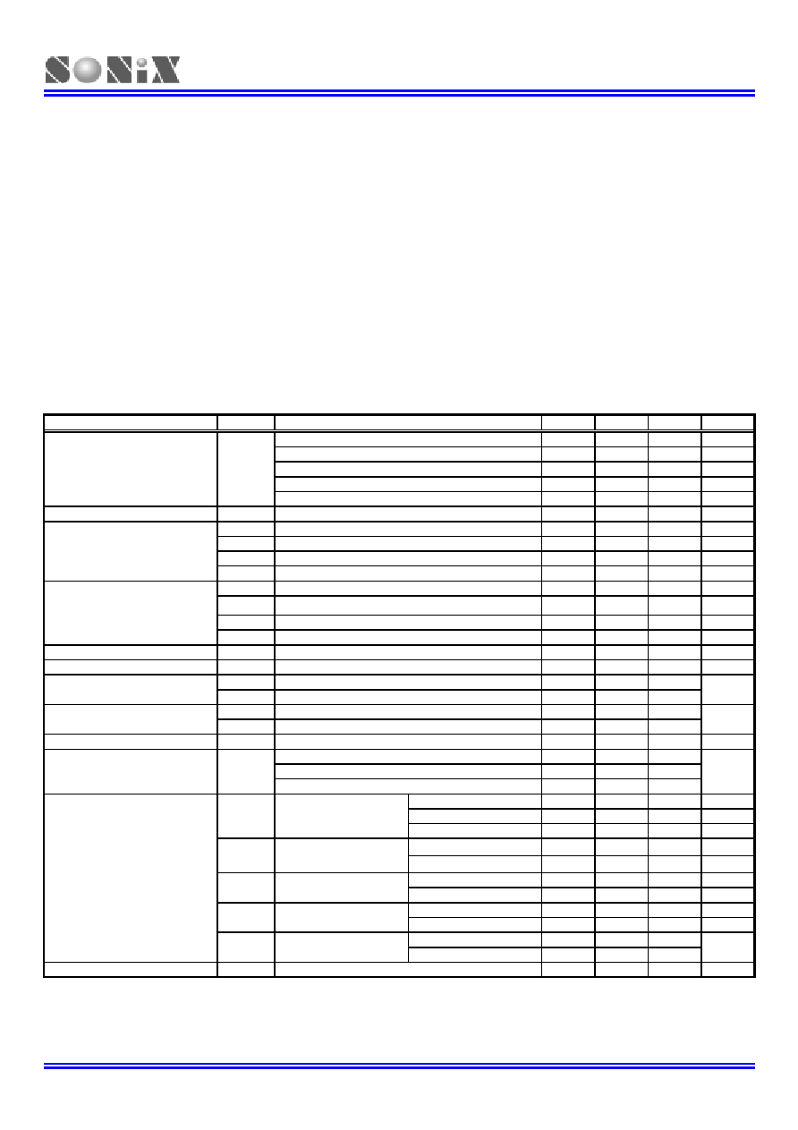
SN8P1602B
8-Bit Micro-Controller
SONiX TECHNOLOGY CO., LTD
Page 69
Version 1.1
1
1
1
3
3
3
ELECTRICAL CHARACTERISTIC
ABSOLUTE MAXIMUM RATING
(All of the voltages referenced to Vss)
Supply voltage (Vdd)............................................................................................................... - 0.3V ~ 6.0V
Input in voltage (Vin)..................................................................................................Vss - 0.2V ~ Vdd + 0.2V
Operating ambient temperature (Top)......................................................................................-20
∞
C ~ + 70
∞
C
Storage ambient temperature (Tstor).......................................................................................-30
∞
C ~ + 125
∞
C
Power consumption (Pc)..................................................................................................................500 mW
STANDARD ELECTRICAL CHARACTERISTIC
SN8P1602B
(All of voltages referenced to Vss, Vdd = 5.0V, Fosc = 3.579545 MHz, ambient temperature is 25
∞
C unless otherwise notice.)
PARAMETER SYM.
DESCRIPTION
MIN.
TYP.
MAX.
UNIT
Normal mode (OSG, Low Power Disable)
2.4
5.0
5.5
V
Normal mode (OSG Enable, Low Power Disable)
2.4
5.0
5.5
V
Normal mode (OSG Disable, Low Power Enable)
2.9
5.0
5.5
V
Normal mode (OSG, Low Power Enable)
2.9
5.0
5.5
V
Operating voltage
Vdd
Programming mode, Vpp = 12.5V
4.5
5.0
5.5
V
RAM Data Retention voltage
Vdr
-
1.5
-
V
ViL1
All input pins except those specified below
Vss
-
0.3Vdd
V
ViL2
Input with Schmitt trigger buffer - Port0
Vss
-
0.2Vdd
V
ViL3
Reset pin ; Xin ( in RC mode )
Vss
-
0.3Vdd
V
Input Low Voltage
ViL4
Xin ( in X'tal mode )
Vss
-
0.3Vdd
V
ViH1
All input pins except those specified below
0.7Vdd
-
Vdd
V
ViH2
Input with Schmitt trigger buffer ≠Port0
0.8Vdd
-
Vdd
V
ViH3
Reset pin ; Xin ( in RC mode )
0.9Vdd
-
Vdd
V
Input High Voltage
ViH4
Xin ( in X'tal mode )
0.7Vdd
-
Vdd
V
Reset pin leakage current
Ilekg
Vin = Vdd
-
-
1
uA
I/O port input leakage current
Ilekg
Pull-up resistor disable, Vin = Vdd
-
-
2
uA
Port1 output source current
IoH
Vop = Vdd ≠ 0.5V
-
12
-
sink current
IoL
Vop = Vss + 0.5V
-
15
-
mA
Port2 output source current
IoH
Vop = Vdd ≠ 0.5V
-
12
-
sink current
IoL
Vop = Vss + 0.5V
-
15
-
mA
INTn trigger pulse width
Tint0
INT0 ~ INT2 interrupt request pulse width
2/fcpu
-
-
cycle
Crystal type or ceramic resonator
32768
4M
16M
VDD = 3V, RC type for external mode
-
6M
-
Oscillator Frequency
Fhosc
VDD = 5V, RC type for external mode
-
10M
-
Hz
Vdd= 5V 4Mhz
-
3
8
mA
Vdd= 3V 4Mhz
-
1
2
mA
Idd1
Run Mode
(Low Power Disable)
Vdd= 3V 32768Hz
-
50
100
uA
Vdd= 5V 4Mhz
-
2
5
mA
Idd2
Run Mode
(Low Power Enable)
Vdd= 3V 4Mhz
-
0.8
2
mA
Vdd= 5V 32KHz Int. RC
-
25
50
uA
Idd3
Slow mode
(Stop High Clock)
Vdd= 3V 16KHz Int. RC
-
7
20
uA
Vdd= 5V
-
1
2
uA
Idd4 Sleep
mode
Vdd= 3V
-
0.6
1
uA
Vdd= 5V 32KHz Int. RC
-
15
30
Supply Current
Idd5
Green Mode
(Stop High Clock)
Vdd= 3V 16KHz Int. RC
3
10
uA
LVD Detect Voltage
Vdet
Low voltage detect level
-
1.8
-
V
Note: Date in Typical (TYP.) column is base on characterization results at 25. This data is design for
guidance only and is not tested.
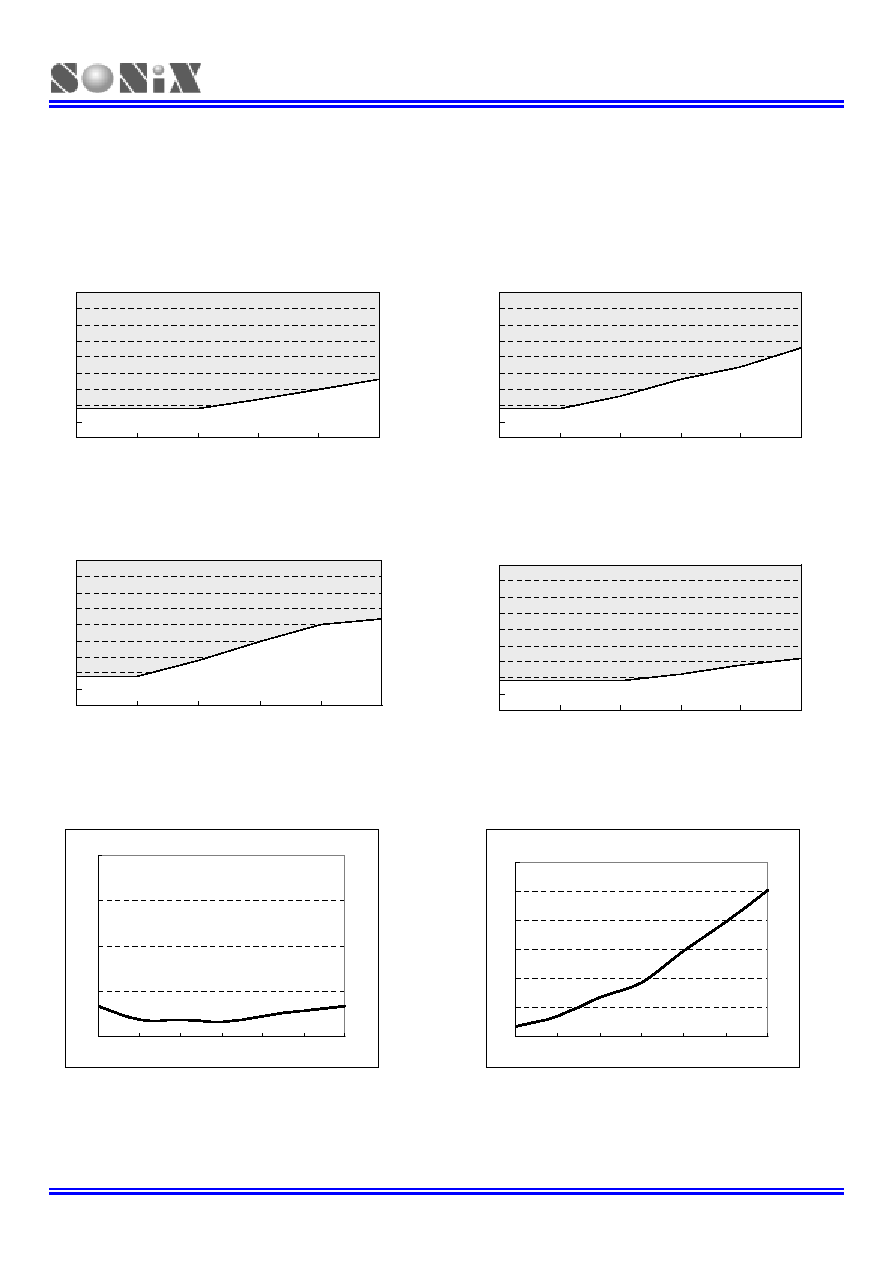
SN8P1602B
8-Bit Micro-Controller
SONiX TECHNOLOGY CO., LTD
Page 70
Version 1.1
CHARACTERISTIC GRAPHS
The Graphs in this section are for design guidance, not tested or guaranteed. In some graphs, the data presented are
outside specified operating range. This is for information only and devices are guaranteed to operate properly only
within the specified range.
SN8P1602B
Figure 13-1Working Voltage vs. Frequency Figure 13-2 Working Voltage vs. Frequency
(OSG, Low Power, Noise Filter Disable) (Noise Filter Enable, OSG, Low Power Disable)
Figure 13-3 Working Voltage vs. Frequency Figure 13-4 Working Voltage vs. Frequency
(Low Power Enable, OSG, Noise Filter Disable) (OSG Enable, Noise filter, Low Power Disable)
Figure 13-5 Typical Stop Mode current (Idd4) vs. VDD Figure 13-6 Typical Slow Mode current (Idd3) vs. VDD
(Stop High Clock)
0.0
0.5
1.0
1.5
2.0
2.0
2.5
3.0
3.5
4.0
4.5
5.0
VDD
uA
0
5
10
15
20
25
30
2.0
2.5
3.0
3.5
4.0
4.5
5.0
VDD
uA
Working area
1.0
1.5
2.0
2.5
3.0
3.5
4.0
4.5
5.0
5.5
2
4
8
12
16
20
Fosc
MHz
VDD
Working area
1.0
1.5
2.0
2.5
3.0
3.5
4.0
4.5
5.0
5.5
2
4
8
12
16
20
Fosc
MHz
VDD
Working area
1.0
1.5
2.0
2.5
3.0
3.5
4.0
4.5
5.0
5.5
2
4
8
12
16
20
Fosc
MHz
VDD
Working area
1.0
1.5
2.0
2.5
3.0
3.5
4.0
4.5
5.0
5.5
2
4
8
12
16
20
Fosc
MHz
VDD

SN8P1602B
8-Bit Micro-Controller
SONiX TECHNOLOGY CO., LTD
Page 71
Version 1.1
Figure 13-7 Typical Run Mode current (Idd1) vs. Fosc Figure 13-8 Typical Run Mode current (Idd2) vs. Fosc
(Low Power Disable) (Low Power Enable)
Figure 13-9 Typical Green Mode current vs. Fosc Figure 13-10 Typical Green Mode current vs. VDD
(Without Stopping High clock) (Stop High clock)
Figure 13-11 Typical IOH vs. VDD Figure 13-12 Typical IOL vs. VDD
0
2
4
6
8
10
2
6
10
14
18
Fosc
MHz
mA
3V
5V
0
2
4
6
8
10
2
6
10
14
18
Fosc
MHz
mA
3V
5V
0.0
1.0
2.0
3.0
4.0
2
6
10
14
18
Fosc
MHz
mA
3V
5V
0
2
4
6
8
10
12
14
16
2.0
2.5
3.0
3.5
4.0
4.5
5.0
VDD
uA
-14
-12
-10
-8
-6
-4
-2
0
2.0
2.5
3.0
3.5
4.0
4.5
5.0
VDD
mA
0
2
4
6
8
10
12
14
16
2.0
2.5
3.0
3.5
4.0
4.5
5.0
VDD
mA

SN8P1602B
8-Bit Micro-Controller
SONiX TECHNOLOGY CO., LTD
Page 72
Version 1.1
Figure 13-13 Typical Slow Mode Frequency vs. VDD
0
5
10
15
20
25
30
2.0
2.5
3.0
3.5
4.0
4.5
5.0
VDD
Fosc
KHz

SN8P1602B
8-Bit Micro-Controller
SONiX TECHNOLOGY CO., LTD
Page 73
Version 1.1
1
1
1
4
4
4
PACKAGE INFORMATION
P-DIP 18 PIN
MIN NOR MAX MIN NOR MAX
SYMBOLS
(inch) (mm)
A - -
0.210
- -
5.334
A1 0.015 -
- 0.381 -
-
A2 0.125
0.130
0.135 3.175 3.302
3.429
D 0.880
0.900
0.920
22.352
22.860
23.368
E 0.300
7.620
E1 0.245
0.250
0.255 6.223
6.350
6.477
L 0.115
0.130
0.150
2.921
3.302
3.810
B
0.335 0.355 0.375 8.509 9.017 9.525
∞ 0∞ 7∞ 15∞ 0∞ 7∞ 15∞
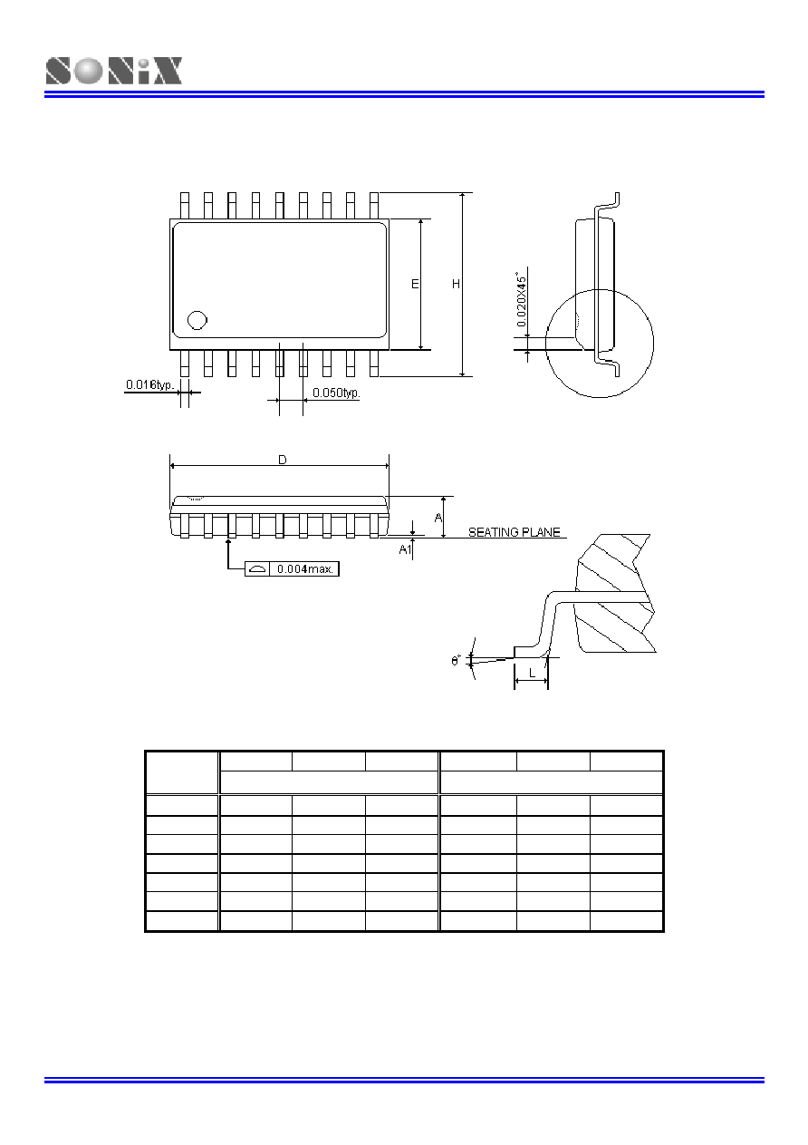
SN8P1602B
8-Bit Micro-Controller
SONiX TECHNOLOGY CO., LTD
Page 74
Version 1.1
SOP 18 PIN
MIN NOR MAX MIN NOR MAX
SYMBOLS
(inch) (mm)
A 0.093
0.099
0.104
2.362
2.502
2.642
A1 0.004
0.008
0.012 0.102 0.203
0.305
D 0.447
0.455
0.463
11.354
11.557
11.760
E 0.291
0.295
0.299
7.391
7.493
7.595
H 0.394
0.407
0.419
10.008
10.325
10.643
L 0.016
0.033
0.050
0.406
0.838
1.270
∞ 0∞ 4∞ 8∞ 0∞ 4∞ 8∞
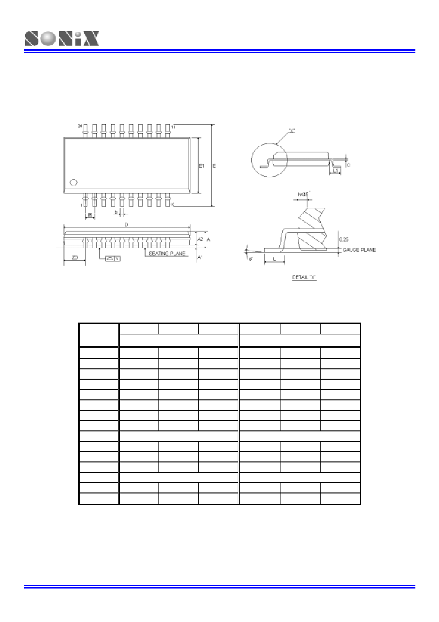
SN8P1602B
8-Bit Micro-Controller
SONiX TECHNOLOGY CO., LTD
Page 75
Version 1.1
SSOP 20 PIN
MIN NOR MAX MIN NOR MAX
SYMBOLS
(inch) (mm)
A 0.053
0.063
0.069
1.350
1.600
1.750
A1 0.004
0.006
0.010 0.100 0.150
0.250
A2 - -
0.059 - -
1.500
b 0.008
0.010
0.012
0.200
0.254
0.300
c 0.007
0.008
0.010
0.180
0.203
0.250
D 0.337
0.341
0.344
8.560
8.660
8.740
E 0.228
0.236
0.244
5.800
6.000
6.200
E1 0.150
0.154
0.157 3.800
3.900
4.000
[e] 0.025
0.635
h 0.010
0.017
0.020
0.250
0.420
0.500
L 0.016
0.025
0.050
0.400
0.635
1.270
L1 0.039
0.041
0.043 1.000
1.050
1.100
ZD 0.059
1.500
Y - -
0.004
- -
0.100
∞ 0∞ - 8∞ 0∞ - 8∞

SN8P1602B
8-Bit Micro-Controller
SONiX TECHNOLOGY CO., LTD
Page 76
Version 1.1
SONIX reserves the right to make change without further notice to any products herein to improve reliability, function or
design. SONIX does not assume any liability arising out of the application or use of any product or circuit described herein;
neither does it convey any license under its patent rights nor the rights of others. SONIX products are not designed,
intended, or authorized for us as components in systems intended, for surgical implant into the body, or other applications
intended to support or sustain life, or for any other application in which the failure of the SONIX product could create a
situation where personal injury or death may occur. Should Buyer purchase or use SONIX products for any such
unintended or unauthorized application. Buyer shall indemnify and hold SONIX and its officers , employees, subsidiaries,
affiliates and distributors harmless against all claims, cost, damages, and expenses, and reasonable attorney fees arising
out of, directly or indirectly, any claim of personal injury or death associated with such unintended or unauthorized use
even if such claim alleges that SONIX was negligent regarding the design or manufacture of the part.
Main Office:
Address: 9F, NO. 8, Hsien Cheng 5th St, Chupei City, Hsinchu, Taiwan R.O.C.
Tel: 886-3-551 0520
Fax: 886-3-551 0523
Taipei Office:
Address: 15F-2, NO. 171, Song Ted Road, Taipei, Taiwan R.O.C.
Tel: 886-2-2759 1980
Fax: 886-2-2759 8180
Hong Kong Office:
Address: Flat 3 9/F Energy Plaza 92 Granville Road, Tsimshatsui East Kowloon.
Tel: 852-2723 8086
Fax: 852-2723 9179
Technical Support by Email:
Sn8fae@sonix.com.tw