 | –≠–ª–µ–∫—Ç—Ä–æ–Ω–Ω—ã–π –∫–æ–º–ø–æ–Ω–µ–Ω—Ç: SN8P2501A | –°–∫–∞—á–∞—Ç—å:  PDF PDF  ZIP ZIP |

SN8P2501A
8-Bit Micro-Controller
SONiX TECHNOLOGY CO., LTD
Preliminary Version 0.2
SN8P2501A
USER'S MANUAL
Preliminary Specification Version 0.2
S
S
O
O
N
N
i
i
X
X
8
8
-
-
B
B
i
i
t
t
M
M
i
i
c
c
r
r
o
o
-
-
C
C
o
o
n
n
t
t
r
r
o
o
l
l
l
l
e
e
r
r
SONIX reserves the right to make change without further notice to any products herein to improve reliability, function or design. SONIX does not
assume any liability arising out of the application or use of any product or circuit described herein; neither does it convey any license under its patent
rights nor the rights of others. SONIX products are not designed, intended, or authorized for us as components in systems intended, for surgical
implant into the body, or other applications intended to support or sustain life, or for any other application in which the failure of the SONIX product
could create a situation where personal injury or death may occur. Should Buyer purchase or use SONIX products for any such unintended or
unauthorized application. Buyer shall indemnify and hold SONIX and its officers, employees, subsidiaries, affiliates and distributors harmless against
all claims, cost, damages, and expenses, and reasonable attorney fees arising out of, directly or indirectly, any claim of personal injury or death
associated with such unintended or unauthorized use even if such claim alleges that SONIX was negligent regarding the design or manufacture of
the part.

SN8P2501A
8-Bit Micro-Controller
SONiX TECHNOLOGY CO., LTD
Page 1
Preliminary Version 0.2
AMENDENT HISTORY
Version Date
Description
VER 0.1
Jan. 2004
Preliminary Version 0.1 first issue
VER 0.2
Jan. 2004
Preliminary Version 0.2. Add SSOP 16 pin package information.

SN8P2501A
8-Bit Micro-Controller
SONiX TECHNOLOGY CO., LTD
Page 2
Preliminary Version 0.2
Table of Content
AMENDENT HISTORY ................................................................................................................. 1
1
1
1
PRODUCT OVERVIEW ..................................................................................................... 6
1.1 SYSTEM
BLOCK DIAGRAM.............................................................................................. 7
1.2 PIN
ASSIGNMENT............................................................................................................. 8
1.3 PIN
DESCRIPTIONS ......................................................................................................... 8
1.4 PIN
CIRCUIT DIAGRAMS.................................................................................................. 9
2
2
2
CENTRAL PROCESSOR UNIT (CPU) ............................................................................ 10
2.1 MEMORY MAP ................................................................................................................ 10
2.1.1 PROGRAM
MEMORY (ROM)................................................................................... 10
2.1.2 DATA
MEMORY (RAM) ............................................................................................ 17
2.1.3 CODE
OPTION TABLE............................................................................................. 18
2.1.4 SYSTEM
REGISTER ................................................................................................ 19
2.2 ACCUMULATOR.............................................................................................................. 22
2.3 PROGRAM
FLAG ............................................................................................................ 23
2.3.1 RESET
FLAG............................................................................................................ 23
2.3.2 CARRY
FLAG ........................................................................................................... 23
2.3.3 DECIMAL
CARRY FLAG .......................................................................................... 23
2.3.4 ZERO FLAG.............................................................................................................. 23
2.4 PROGRAM
COUNTER .................................................................................................... 24
2.4.1 ONE
ADDRESS SKIPPING ...................................................................................... 24
2.4.2 MULTI-ADDRESS JUMPING.................................................................................... 25
2.5 ADDRESSING MODE...................................................................................................... 26
2.5.1 IMMEDIATE
ADDRESSING MODE.......................................................................... 26
2.5.2 ........................................................................................................................................ 26
2.5.3 DIRECTLY
ADDRESSING MODE ............................................................................ 26
2.5.4 ........................................................................................................................................ 26
2.5.5 INDIRECTLY
ADDRESSING MODE ........................................................................ 26
2.6 STACK
OPERATIONS..................................................................................................... 27
2.6.1 OVERVIEW............................................................................................................... 27
2.6.2 STACK
REGISTERS ................................................................................................ 28
2.6.3 STACK
OPERATION EXAMPLE .............................................................................. 29

SN8P2501A
8-Bit Micro-Controller
SONiX TECHNOLOGY CO., LTD
Page 3
Preliminary Version 0.2
3
3
3
RESET ............................................................................................................................. 30
3.1 OVERVIEW...................................................................................................................... 30
3.2 EXTERNAL
RESET
DESCRIPTION ................................................................................ 31
3.3
LOW VOLTAGE DETECTOR (LVD) DESCRIPTION....................................................... 32
4
4
4
OSCILLATOR AND SYSTEM CLOCK............................................................................ 33
4.1 OVERVIEW...................................................................................................................... 33
4.2 CLOCK
BLOCK
DIAGRAM .............................................................................................. 33
4.3 OSCM
REGISTER
DESCRIPTION.................................................................................. 34
4.4
EXTERNAL SYSTEM OSCILLATOR CIRCUITS ............................................................. 35
4.4.1 OSCILLATOR
FREQUENCY MEASUREMENT ....................................................... 36
4.4.2 INTERNAL
LOW-SPEED RC OSCILLATOR ............................................................ 37
5
5
5
SYSTEM OPERATION MODE ........................................................................................ 38
5.1 OVERVIEW...................................................................................................................... 38
5.2 NORMAL MODE .............................................................................................................. 38
5.3 SLOW MODE................................................................................................................... 38
5.4 GREEN MODE................................................................................................................. 38
5.5 POWER
DOWN MODE.................................................................................................... 38
5.6 SYSTEM
MODE
CONTROL ............................................................................................ 39
5.6.1 SYSTEM
MODE SWITCHING .................................................................................. 40
5.7 WAKEUP.......................................................................................................................... 42
5.7.1 OVERVIEW............................................................................................................... 42
5.7.2 WAKEUP
TIME ......................................................................................................... 42
5.7.3
P1W WAKEUP CONTROL REGISTER .................................................................... 42
6
6
6
INTERRUPT..................................................................................................................... 43
6.1 OVERVIEW...................................................................................................................... 43
6.2 INTEN
INTERRUPT
ENABLE REGISTER....................................................................... 43
6.3
INTRQ INTERRUPT REQUEST REGISTER ................................................................... 44
6.4 INTERRUPT
OPERATION DESCRIPTION ..................................................................... 44

SN8P2501A
8-Bit Micro-Controller
SONiX TECHNOLOGY CO., LTD
Page 4
Preliminary Version 0.2
6.4.1
GIE GLOBAL INTERRUPT OPERATION ................................................................. 44
6.4.2
INT0 (P0.0) INTERRUPT OPERATION .................................................................... 45
6.4.3 T0
INTERRUPT OPERATION .................................................................................. 46
6.4.4 TC0
INTERRUPT OPERATION................................................................................ 47
6.4.5 MULTI-INTERRUPT OPERATION............................................................................ 48
7
7
7
I/O PORT ......................................................................................................................... 49
7.1 I/O
PORT MODE.............................................................................................................. 49
7.2
I/O PULL UP REGISTER ................................................................................................. 50
7.3 I/O
OPEN-DRAIN REGISTER.......................................................................................... 50
7.4
I/O PORT DATA REGISTER............................................................................................ 51
8
8
8
TIMERS............................................................................................................................ 52
8.1 WATCHDOG
TIMER........................................................................................................ 52
8.2 TIMER
0 (T0) ................................................................................................................... 53
8.2.1 OVERVIEW............................................................................................................... 53
8.2.2 T0M
MODE
REGISTER............................................................................................ 53
8.2.3 T0C
COUNTING REGISTER .................................................................................... 54
8.3 TIMER/COUNTER 0 (TC0) .............................................................................................. 55
8.3.1 OVERVIEW............................................................................................................... 55
8.3.2 TC0M
MODE REGISTER ......................................................................................... 56
8.3.3 TC0C
COUNTING REGISTER ................................................................................. 57
8.4 BUZZER
OUTPUT ........................................................................................................... 58
8.4.1 TC0OUT
FREQUENCY TABLE ................................................................................ 59
8.5
PWM FUNCTION DESCRIPTION.................................................................................... 61
8.5.1 OVERVIEW............................................................................................................... 61
8.5.2 PWM
PROGRAM
DESCRIPTION ............................................................................ 62
9
9
9
INSTRUCTION SET TABLE............................................................................................ 63
1
1
1
0
0
0
ELECTRICAL CHARACTERISTIC........................................................................... 64
10.1 ABSOLUTE
MAXIMUM RATING ..................................................................................... 64

SN8P2501A
8-Bit Micro-Controller
SONiX TECHNOLOGY CO., LTD
Page 5
Preliminary Version 0.2
10.2 ELECTRICAL
CHARACTERISTIC................................................................................... 64
1
1
1
1
1
1
PACKAGE INFORMATION...................................................................................... 65
11.1 P-DIP
14 PIN.................................................................................................................... 65
11.2 SOP
14 PIN...................................................................................................................... 66
11.3 SSOP
16 PIN ................................................................................................................... 67
SN8P2501A
8-Bit Micro-Controller
SONiX TECHNOLOGY CO., LTD
Page 6
Preliminary Version 0.2
1
1
1
PRODUCT OVERVIEW
FEATURES
Memory configuration
One channel PWM output. (PWM0)
OTP ROM size: 1K * 16 bits.
One channel Buzzer output. (BZ0)
RAM size: 48 * 8 bits.
Two 8-bit timer counters. (T0, TC0).
One RTC timer. (T0)
Four levels stack buffer.
On chip watchdog timer.
I/O pin configuration
Three system clocks
Input only: P1.1.
External high clock: RC type up to 10 MHz
Bi-directional: P0, P1, P2, P5.
External high clock: Crystal type up to 16 MHz
Wakeup: P0, P1.
Internal low clock: RC type 16KHz(3V), 32KHz(5V)
Pull-up resisters: P0, P1, P2, P5.
Internal high clock: 16MHz RC type.
External interrupt: P0.
One pin with open-drain: P1.0.
Four operating modes
Normal mode: Both high and low clock active
3 interrupt sources
Slow mode: Low clock only
Two internal interrupts: T0, TC0.
Sleep mode: Both high and low clock stop
One external interrupts: INT0.
Green mode: Periodical wakeup by T0 Timer
Powerful instructions
Package (Chip form support)
One clock per machine cycle
PDIP 14 pins
Most of instructions are one cycle only.
SOP 14 pins
All ROM area JMP instruction.
SSOP 16 pins
All ROM area lookup table function (MOVC)
FEATURES TABLE
Timer
PWM
CHIP
ROM RAM Stack
T0 TC0
RTC I/O
Green
Mode Buzzer
Wakeup
Pin No.
Package
SN8P2501A 1K*16 48 4 V V V 12
V V 5 DIP14/SOP14/SSOP16
SN8P1602B 1K*16 48 4 - V
-
14
V
-
6 DIP18/SOP18/SSOP20
SN8P2602A 1K*16 48
4
V
V
-
15
V
V
7
DIP18/SOP18/SSOP20

SN8P2501A
8-Bit Micro-Controller
SONiX TECHNOLOGY CO., LTD
Page 7
Preliminary Version 0.2
1.1 SYSTEM BLOCK DIAGRAM
PC
IR
R
O
M
H-OSC
TIMING GENERATOR
RAM
SYSTEM REGISTER
ALU
ACC
INTERRUPT
CONTROL
TIMER & COUNTER
PORT 0
PORT 2
PORT 1
FLAGS
Internal
Low
RC
POR
Watch
Dog
SN8P2501A
PWM
PORT 5
PWM & BUZZER
Internal
High
RC
PC
IR
R
O
M
H-OSC
TIMING GENERATOR
RAM
SYSTEM REGISTER
ALU
ACC
INTERRUPT
CONTROL
TIMER & COUNTER
PORT 0
PORT 2
PORT 1
FLAGS
Internal
Low
RC
POR
Watch
Dog
SN8P2501A
PWM
PORT 5
PWM & BUZZER
Internal
High
RC

SN8P2501A
8-Bit Micro-Controller
SONiX TECHNOLOGY CO., LTD
Page 8
Preliminary Version 0.2
1.2 PIN
ASSIGNMENT
SN8P2501AP (P-DIP 14 pins)
SN8P2501AS (SOP 14 pins)
SN8P2501AX (SSOP 16 pins)
P2.2
1 U 14
P2.3
P2.1
2 13
P2.4
P2.0
3 12
P2.5
VDD
4 11
VSS
XIN/P1.3
5 10
P0.0/INT0
XOUT/P1.2
6 9
P1.0
VPP/RST/P1.1
7 8
P5.4/PWM0/BZ0
SN8P2501AP
SN8P2501AS
P2.2
1 U 16
P2.3
P2.1
2 15
P2.4
P2.0
3 14
P2.5
VDD
4 13
VSS
VDD
5 12
VSS
XIN/P1.3
6 11
P0.0/INT0
XOUT/P1.2
7 10
P1.0
VPP/RST/P1.1
8 9
P5.4/PWM0/BZ0
SN8P2501AX
1.3 PIN
DESCRIPTIONS
SN8P2501A
PAD NAME
TYPE
DESCRIPTION
VDD, VSS
P
Power supply input pins. Place the 0.1µF bypass capacitor between the VDD and VSS pin.
P1.1/RST/VPP I,
P
P1.1: Input only pin (Schmitt trigger) if disable external reset function.
P1.1 without build-in pull-up resister
RST: System reset input pin. Schmitt trigger structure, low active, normal stay to "high".
VPP: OTP programming pin.
P1.3/XIN I/O
P1.3: I/O pin (Schmitt trigger) if high clock select internal high RC oscillator / Built-in pull-up
resister.
XIN: Oscillator input pin if high clock select external oscillator (crystal or RC type).
P1.2/XOUT I/O
P1.2: I/O pin (Schmitt trigger) if high clock select internal high RC oscillator or external RC
type oscillator / Built-in pull-up resister.
XOUT: Oscillator output pin if high clock select external crystal type oscillator.
P0.0/INT0 I/O
P0.0: I/O pin (Schmitt trigger) and shared with INT0 trigger pin (Schmitt trigger) / Built-in
pull-up resister.
TC0 event counter clock input pin.
P1.0
I/O Port 1.0 bi-direction pin (Schmitt trigger) / Built-in pull-up resister / Open-Drain pin.
P5.4/BZ0/PWM0 I/O
Port 5.4 bi-direction pin (Schmitt trigger) / Built-in pull-up resister.
TC0 ˜ 2 signal output pin for buzzer and PWM output pin.
P2.0~P2.5
I/O Port 2.0~Port 2.5 bi-direction pins (Schmitt trigger) / Built-in pull-up resisters.
SN8P2501A
8-Bit Micro-Controller
SONiX TECHNOLOGY CO., LTD
Page 9
Preliminary Version 0.2
1.4 PIN CIRCUIT DIAGRAMS
Port 0, 2, 5 structure:
Pull-Up
PnM, PnUR
Pin
Int. bus
Output
Latch
PnM
PnM
Pull-Up
PnM, PnUR
Pin
Int. bus
Output
Latch
PnM
PnM
PnM
PnM
Port 1.0 structure:
Pull-Up
PnM, PnUR
Pin
Int. bus
Output
Latch
PnM
PnM
Open-Drain
P1OC
Pull-Up
PnM, PnUR
Pin
Pin
Int. bus
Output
Latch
PnM
PnM
PnM
PnM
Open-Drain
P1OC
P1OC
Port 1.2 and Port 1.3 structure:
Pull-Up
PnM, PnUR
Pin
Int. bus
Output
Latch
PnM
PnM
Oscillator
Code Option
Int. Osc.
Pull-Up
PnM, PnUR
Pin
Pin
Int. bus
Output
Latch
PnM
PnM
PnM
Oscillator
Code Option
Int. Osc.
Port 1.1 structure:
Int. bus
Int. Rst
Pin
Ext. Rst Code Option
Int. bus
Int. Rst
Pin
Pin
Ext. Rst Code Option
SN8P2501A
8-Bit Micro-Controller
SONiX TECHNOLOGY CO., LTD
Page 10
Preliminary Version 0.2
2
2
2
CENTRAL PROCESSOR UNIT (CPU)
2.1 MEMORY
MAP
2.1.1 PROGRAM MEMORY (ROM)
1K words ROM
ROM
0000H
Reset vector
User reset vector
0001H
Jump to user start address
0002H
Jump to user start address
0003H
General purpose area
Jump to user start address
0004H
0005H
0006H
0007H
Reserved
0008H
Interrupt vector
User interrupt vector
0009H User
program
.
.
000FH
0010H
0011H
.
.
.
.
.
03FBH
General purpose area
End of user program
03FCH
03FDH
03FEH
03FFH
Reserved

SN8P2501A
8-Bit Micro-Controller
SONiX TECHNOLOGY CO., LTD
Page 11
Preliminary Version 0.2
USER RESET VECTOR ADDRESS (0000H)
A one-word vector address area is used to execute system reset. After power on reset or watchdog timer overflow
reset, then the chip will restart the program from address 0000h and all system registers will be set as default values.
The following example shows the way to define the reset vector in the program memory.
Programming Tip: Defining Reset Vector
CHIP SN8P2501A
ORG
0
;
0000H
JMP
START
; Jump to user program address.
.
; 0004H ~ 0007H are reserved
ORG
10H
START:
; 0010H, The head of user program.
.
; User program
.
.
.
ENDP
; End of program
INTERRUPT VECTOR ADDRESS (0008H)
A 1-word vector address area is used to execute interrupt request. If any interrupt service executes, the program
counter (PC) value is stored in stack buffer and jump to 0008h of program memory to execute the vectored interrupt.
Users have to define the interrupt vector. The following example shows the way to define the interrupt vector in the
program memory.
Programming Tip: Defining Interrupt Vector (Example 1)
CHIP SN8P2501A
.DATA ACCBUF
PFLAGBUF
.CODE
ORG
0
;
0000H
JMP
START
; Jump to user program address.
.
; 0004H ~ 0007H are reserved
ORG
8
; Interrupt service routine
B0XCH
A, ACCBUF
; B0XCH doesn't change C, Z flag
B0MOV
A,
PFLAG
B0MOV
PFLAGBUF, A
; Save PFLAG register in a buffer
.
.
B0MOV
A,
PFLAGBUF
B0MOV
PFLAG, A
; Restore PFLAG register from buffer
B0XCH
A, ACCBUF
; B0XCH doesn't change C, Z flag
RETI
; End of interrupt service routine
START:
; The head of user program.
.
; User program
.
JMP
START
; End of user program
ENDP
; End of program

SN8P2501A
8-Bit Micro-Controller
SONiX TECHNOLOGY CO., LTD
Page 12
Preliminary Version 0.2
Programming Tip: Defining Interrupt Vector (Example 2)
CHIP SN8P2501A
.DATA ACCBUF
PFLAGBUF
.CODE
ORG
0
;
0000H
JMP
START
; Jump to user program address.
.
; 0001H ~ 0007H are reserved
ORG
08
JMP
MY_IRQ
; 0008H, Jump to interrupt service routine address
ORG
10H
START:
; 0010H, The head of user program.
.
; User program
.
.
JMP
START
; End of user program
MY_IRQ:
;The head of interrupt service routine
B0XCH
A, ACCBUF
; B0XCH doesn't change C, Z flag
B0MOV
A,
PFLAG
B0MOV
PFLAGBUF, A
; Save PFLAG register in a buffer
.
.
B0MOV
A,
PFLAGBUF
B0MOV
PFLAG, A
; Restore PFLAG register from buffer
B0XCH
A, ACCBUF
; B0XCH doesn't change C, Z flag
RETI
; End of interrupt service routine
ENDP
; End of program
Remark: It is easy to understand the rules of SONIX program from demo programs given above. These
points are as following:
1. The address 0000H is a "JMP" instruction to make the program starts from the beginning.
2. The 0004H~0007H are reserved. Users is NOT allow to use 0004H~0007H addresses. We strongly
suggest users DO NOT take this value into the Check Sum. For detailed information, please check the
following Checksum Calculation section.

SN8P2501A
8-Bit Micro-Controller
SONiX TECHNOLOGY CO., LTD
Page 13
Preliminary Version 0.2
CHECKSUM CALCULATION
The ROM addresses 0004H~0007H and last address are reserved area. User should avoid these addresses
(0004H~0007H and last address) when calculate the Checksum value.
Example:
The demo program shows how to avoid 0004H~0007H when calculated Checksum from 00H to the end of
user's code
MOV
A,#END_USER_CODE$L
B0MOV
END_ADDR1,A
;save low end address to end_addr1
MOV
A,#END_USER_CODE$M
B0MOV
END_ADDR2,A
;save middle end address to end_addr2
CLR
Y
;set Y to 00H
CLR
Z
;set Z to 00H
@@:
CALL
YZ_CHECK
;call function of check yz value
MOVC
;
B0BSET
FC ;clear
C
flag
ADD
DATA1,A
;add A to Data1
MOV
A,R
ADC
DATA2,A
;add R to Data2
JMP
END_CHECK
;check if the YZ address = the end of code
AAA:
INCMS
Z
;Z=Z+1
JMP
@B
;if Z!= 00H calculate to next address
JMP
Y_ADD_1
;if Z=00H increase Y
END_CHECK:
MOV
A,END_ADDR1
CMPRS
A,Z
;check if Z = low end address
JMP
AAA
;if Not jump to checksum calculate
MOV
A,END_ADDR2
CMPRS
A,Y
;if Yes, check if Y = middle end address
JMP
AAA
;if Not jump to checksum calculate
JMP
CHECKSUM_END
;if Yes checksum calculated is done.
YZ_CHECK:
;check if YZ=0004H
MOV
A,#04H
CMPRS
A,Z
;check if Z=04H
RET
;if Not return to checksum calculate
MOV
A,#00H
CMPRS
A,Y
;if Yes, check if Y=00H
RET
;if Not return to checksum calculate
INCMS
Z
;if Yes, increase 4 to Z
INCMS
Z
INCMS
Z
INCMS
Z
RET
;set YZ=0008H then return
Y_ADD_1:
INCMS
Y
;increase
Y
NOP
JMP
@B
;jump to checksum calculate
CHECKSUM_END:
..........
..........
END_USER_CODE:
;Label of program end

SN8P2501A
8-Bit Micro-Controller
SONiX TECHNOLOGY CO., LTD
Page 14
Preliminary Version 0.2
GENERAL PURPOSE PROGRAM MEMORY AREA
The ROM location 0009H~03FBH are used as general-purpose memory. The area is to store both instruction's
op-code and look-up table data. The SN8P2501A includes jump table function by using program counter (PC) and
look-up table function by using ROM code registers (R, Y, Z).
LOOK-UP TABLE DESCRIPTION
In the ROM's data lookup function, Y register is pointed to the bit 8~bit 15 and Z register to the bit 0~bit 7 data of ROM
address. After MOVC instruction executed, the low-byte data will be stored in ACC and high-byte data stored in R
register.
Example: To look up the ROM data located "TABLE1".
B0MOV
Y, #TABLE1$M
; To set lookup table1's middle address
B0MOV
Z, #TABLE1$L
; To set lookup table1's low address.
MOVC
; To lookup data, R = 00H, ACC = 35H
;
; Increment the index address for next address
INCMS Z
;
Z+1
JMP
@F
; Not overflow
INCMS
Y
; Z overflow (FFH 00), Y=Y+1
NOP
;
;
@@:
MOVC
; To lookup data, R = 51H, ACC = 05H.
.
.
;
TABLE1:
DW
0035H
; To define a word (16 bits) data.
DW
5105H
; "
DW
2012H
; "
CAUSION: The Y register will not increase automatically when Z register crosses boundary from 0xFF to
0x00. Therefore, user must take care
such
situation to avoid
loop-up table errors.
If
Z
register
overflows, Y register must be added one. The following INC_YZ macro shows a simple method to process
Y and Z registers automatically.
Example: INC_YZ Macro
INC_YZ
MACRO
INCMS
Z
; Z+1
JMP
@F
; Not overflow
INCMS
Y
; Y+1
NOP
; Not overflow
@@:
ENDM

SN8P2501A
8-Bit Micro-Controller
SONiX TECHNOLOGY CO., LTD
Page 15
Preliminary Version 0.2
The other example of loop-up table is to add Y or Z index register by accumulator. Please be careful if "carry" happen.
Example: Increase Y and Z register by B0ADD/ADD instruction
B0MOV
Y, #TABLE1$M
; To set lookup table's middle address.
B0MOV
Z, #TABLE1$L
; To set lookup table's low address.
B0MOV
A, BUF
; Z = Z + BUF.
B0ADD Z,
A
B0BTS1
FC
; Check the carry flag.
JMP
GETDATA
; FC = 0
INCMS
Y
; FC = 1. Y+1.
NOP
GETDATA:
;
MOVC
; To lookup data. If BUF = 0, data is 0x0035
; If BUF = 1, data is 0x5105
; If BUF = 2, data is 0x2012
.
.
.
.
;
TABLE1:
DW
0035H
; To define a word (16 bits) data.
DW
5105H
; "
DW
2012H
; "

SN8P2501A
8-Bit Micro-Controller
SONiX TECHNOLOGY CO., LTD
Page 16
Preliminary Version 0.2
JUMP TABLE DESCRIPTION
The jump table operation is one of multi-address jumping function. Add low-byte program counter (PCL) and ACC
value to get one new PCL. The new program counter (PC) points to a series jump instructions as a listing table. It is
easy to make a multi-jump program depends on the value of the accumulator (A).
Example :
ORG
0X0100
; The jump table is from the head of the ROM boundary
B0ADD
PCL, A
; PCL = PCL + ACC, the PCH can't be changed.
JMP
A0POINT
; ACC = 0, jump to A0POINT
JMP
A1POINT
; ACC = 1, jump to A1POINT
JMP
A2POINT
; ACC = 2, jump to A2POINT
JMP
A3POINT
; ACC = 3, jump to A3POINT
SONIX provides a macro for safe jump table function. This macro will check the ROM boundary and move the jump
table to the right position automatically. The side effect of this macro maybe wastes some ROM size.
@JMP_A MACRO
VAL
IF
(($+1) !& 0XFF00) !!= (($+(VAL)) !& 0XFF00)
JMP
($ | 0XFF)
ORG
($ | 0XFF)
ENDIF
ADD
PCL,
A
ENDM
Note: "VAL" is the number of the jump table listing number.
Example: "@JMP_A" application in SONIX macro file called "MACRO3.H".
B0MOV
A, BUF0
; "BUF0" is from 0 to 4.
@JMP_A
5
; The number of the jump table listing is five.
JMP
A0POINT
; If ACC = 0, jump to A0POINT
JMP
A1POINT
; ACC = 1, jump to A1POINT
JMP
A2POINT
; ACC = 2, jump to A2POINT
JMP
A3POINT
; ACC = 3, jump to A3POINT
JMP
A4POINT
; ACC = 4, jump to A4POINT
If the jump table position is from 00FDH to 0101H, the "@JMP_A" macro will make the jump table to start from 0100h.

SN8P2501A
8-Bit Micro-Controller
SONiX TECHNOLOGY CO., LTD
Page 17
Preliminary Version 0.2
2.1.2 DATA MEMORY (RAM)
48 X 8-bit RAM
Address
RAM location
000h
"
"
"
"
"
02Fh
General purpose area
080h
"
80h~FFh of Bank 0 store system
registers (128 bytes).
"
"
"
"
System register
BANK 0
0FFh
End of bank 0 area

SN8P2501A
8-Bit Micro-Controller
SONiX TECHNOLOGY CO., LTD
Page 18
Preliminary Version 0.2
2.1.3 CODE OPTION TABLE
Code Option
Content
Function Description
RC
Low cost RC for external high clock oscillator and XOUT becomes to
general purpose I/O (P1.2).
32K X'tal
Low frequency, power saving crystal (e.g. 32.768KHz) for external high
clock oscillator.
12M X'tal
High speed crystal /resonator (e.g. 12MHz) for external high clock
oscillator.
4M X'tal
Standard crystal /resonator (e.g. 4M) for external high clock oscillator.
IHRC_16M
Internal high RC 16MHz and external oscillator pins as general purpose
I/O (XIN to P1.3, XOUT to P1.2).
High_Clk
IHRC_RTC
Internal high RC 16MHz with RTC function and external oscillator pins
connect with 32.768KHz crystal to generating real time clock.
Always_On
Watchdog timer always on even in power down and green mode.
Enable
Enable watchdog timer. Watchdog timer stops in power down mode and
green mode.
Watch_Dog
Disable Disable
Watchdog
function.
Fosc/1
Instruction cycle is oscillator clock.
Notice: In Fosc/1, Low Power must be disabled
Fosc/2
Instruction cycle is 2 oscillator clocks.
Notice: In Fosc/2 Low Power must be disabled
Fosc/4
Instruction cycle is 4 oscillator clocks.
Fosc/8
Instruction cycle is 8 oscillator clocks.
Fosc/16
Instruction cycle is 16 oscillator clocks.
Fosc/32
Instruction cycle is 32 oscillator clocks.
Fcpu
Fosc/64
Instruction cycle is 64 oscillator clocks.
-2MHz
Internal high RC 16MHz typical frequency - 2MHz.
-1MHz
Internal high RC 16MHz typical frequency -1MHz.
Normal
Internal high RC 16MHz typical frequency.
+1MHz
Internal high RC 16MHz typical frequency + 1MHz.
16M_IHRC
+2MHz
Internal high RC 16MHz typical frequency + 2MHz.
Reset
Enable External reset pin.
Reset_Pin
P11
Enable P1.1 input only without pull-up resister.
Enable
Enable ROM code Security function.
Security
Disable
Disable ROM code Security function.
Enable
Enable Low Power function to save Operating current.
Low Power
Disable Normal.
Enable
Enable Noise Filter and the Fcpu is Fosc/4~Fosc/64.
Noise_Filter
Disable
Disable Noise Filter and the Fcpu is Fosc/1~Fosc/64.
Notice:
If users define watchdog as "Always_On", assembler will Enable "Watch_Dog" automatically.
Enable "Low Power" option will reduce operating current except in "High_Clk = 32K X'tal" and
slow mode.
Enable "Low Power" will limit the Fcpu = Fosc/4 ~ Fosc/64.
Enable "Noise_Filter" will limit the Fcpu = Fosc/4 ~ Fosc/64.
Fcpu code option is only available for High Clock.
SN8P2501A
8-Bit Micro-Controller
SONiX TECHNOLOGY CO., LTD
Page 19
Preliminary Version 0.2
2.1.4 SYSTEM REGISTER
BYTES of SYSTEM REGISTER
SN8P2501A
0 1 2 3 4 5 6 7 8 9 A B C D E F
8
- - R
Z
Y -
PFLAG
-
OPTION
- - - - - - -
9
- - - - - - - - - - - - - - - -
A
- - - - - - - - - - - - - - - -
B
- - - - - - - -
P0M - - - - - - PEDGE
C
P1W P1M P2M -
- P5M -
- INTRQ
INTEN OSCM
- WDTR
TC0R
PCL
PCH
D
P0 P1 P2 - - P5 - - T0M T0C
TC0M
TC0C - - - STKP
E
P0UR P1UR P2UR -
- P5UR
-
@YZ
-
P1OC
-
-
-
-
-
-
F
- - - - - - - -
STK3L
STK3H STK2L STK2H
STK1L
STK1H STK0L STK0H
Description
PFLAG = ROM page and special flag register.
R = Working register and ROM look-up data buffer.
P1W = Port 1 wakeup register.
Y, Z = Working, @YZ and ROM addressing register.
PEDGE = P0.0 edge direction register.
OPTION = RTC period selection register.
PnM = Port n input/output mode register.
Pn = Port n data buffer.
P1OC = Port 1 open-drain control register.
PnUR = Port n pull-up resister control register.
INTRQ = Interrupt request register.
INTEN = Interrupt enable register.
OSCM = Oscillator mode register.
PCH, PCL = Program counter.
T0M = T0 mode register.
T0C = TC0 counting register.
TC0M = TC0 mode register.
TC0C = TC0 counting register.
TC0R = TC0 auto-reload data buffer.
WDTR = Watchdog timer clear register.
STKP = Stack pointer buffer.
STK0~STK3 = Stack 0 ~ stack 3 buffer.
@YZ = RAM YZ indirect addressing index pointer.

SN8P2501A
8-Bit Micro-Controller
SONiX TECHNOLOGY CO., LTD
Page 20
Preliminary Version 0.2
BITS of SYSTEM REGISTER
SN8P2501A system register table
Address
Bit7 Bit6 Bit5 Bit4 Bit3 Bit2 Bit1 Bit0
R/W Remarks
082H RBIT7 RBIT6 RBIT5 RBIT4 RBIT3 RBIT2 RBIT1 RBIT0 R/W
R
083H ZBIT7 ZBIT6 ZBIT5 ZBIT4 ZBIT3 ZBIT2 ZBIT1 ZBIT0
R/W
Z
084H YBIT7 YBIT6 YBIT5 YBIT4 YBIT3 YBIT2 YBIT1 YBIT0 R/W
Y
086H NT0 NPD -
-
-
C
DC
Z R/W
PFLAG
088H
- - - -
RTC1
RTC0
- -
R/W
OPTION
0B8H
- - - - - - -
P00M
R/W
P0M
0BFH -
-
- P00G1
P00G0 -
-
- R/W
PEDGE
0C0H
- - - -
P13W
P12W
P11W P10W W
P1W
wakeup
register
0C1H
- - - -
P13M
P12M
-
P10M
R/W
P1M
I/O
direction
0C2H -
-
P25M P24M P23M P22M P21M P20M
R/W
P2M
I/O
direction
0C5H
- - -
P54M
- - - -
R/W
P5M
I/O
direction
0C8H
- -
TC0IRQ
T0IRQ
- - -
P00IRQ
R/W
INTRQ
0C9H
- -
TC0IEN
T0IEN
- - -
P00IEN
R/W
INTEN
0CAH 0
0
0 CPUM1
CPUM0
CLKMD
STPHX 0 R/W
OSCM
0CCH WDTR7 WDTR6 WDTR5 WDTR4
WDTR3
WDTR2
WDTR1
WDTR0 W
WDTR
0CDH TC0R7 TC0R6 TC0R5 TC0R4 TC0R3 TC0R2 TC0R1 TC0R0 W
TC0R
0CEH PC7 PC6 PC5 PC4 PC3 PC2 PC1 PC0
R/W
PCL
0CFH
- - - - - -
PC9
PC8
R/W
PCH
0D0H
- - - - - - -
P00
R/W
P0
data
buffer
0D1H
- - - -
P13
P12
P11
P10
R/W
P1
data
buffer
0D2H -
- P25 P24 P23 P22 P21 P20
R/W
P2
data
buffer
0D5H
- - -
P54
- - - -
R/W
P5
data
buffer
0D8H T0ENB T0rate2 T0rate1 T0rate0
-
-
-
T0TB R/W
T0M
0D9H T0C7 T0C6 T0C5 T0C4 T0C3 T0C2 T0C1 T0C0
R/W
T0C
0DAH TC0ENB
TC0rate2
TC0rate1
TC0rate0
TC0CKS
ALOAD0
TC0OUT
PWM0OUT
R/W
TC0M
0DBH TC0C7 TC0C6 TC0C5 TC0C4 TC0C3 TC0C2 TC0C1 TC0C0 R/W
TC0C
0DFH
GIE
- - - -
STKPB2
STKPB1
STKPB0
R/W
STKP
stack
pointer
0E0H
- - - - - - -
P00R
W
P0
pull-up
register
0E1H
- - - -
P13R
P12R
-
P10R
W
P1
pull-up
register
0E2H -
- P25R P24R P23R P22R P21R P20R W
P2
pull-up
register
0E5H
- - -
P54R
- - - -
W
P5
pull-up
register
0E7H @YZ7 @YZ6 @YZ5 @YZ4 @YZ3 @YZ2 @YZ1 @YZ0 R/W
@YZ
index
pointer
0E9H
- - - - - - -
P10OC
W
P1OCopen-drain
0F8H S3PC7 S3PC6 S3PC5 S3PC4 S3PC3 S3PC2 S3PC1 S3PC0 R/W
STK3L
0F9H
- - - - - -
S3PC9
S3PC8
R/W
STK3H
0FAH S2PC7 S2PC6 S2PC5 S2PC4 S2PC3 S2PC2 S2PC1 S2PC0 R/W
STK2L
0FBH
- - - - - -
S2PC9
S2PC8
R/W
STK2H
0FCH S1PC7 S1PC6 S1PC5 S1PC4 S1PC3 S1PC2 S1PC1 S1PC0 R/W
STK1L
0FDH
- - - - - -
S1PC9
S1PC8
R/W
STK1H
0FEH S0PC7 S0PC6 S0PC5 S0PC4 S0PC3 S0PC2 S0PC1 S0PC0 R/W
STK0L
0FFH
- - - - - -
S0PC9
S0PC8
R/W
STK0H
Note
a):
To avoid system error, please be sure to put all the "0" and "1" as it indicates in the above table
b). All of register names had been declared in SN8ASM assembler.
c). One-bit name had been declared in SN8ASM assembler with "F" prefix code.
d). "b0bset", "b0bclr", "bset", "bclr" instructions are only available to the "R/W" registers.
e). For detail description, please refer to the "System Register Quick Reference Table"
SN8P2501A
8-Bit Micro-Controller
SONiX TECHNOLOGY CO., LTD
Page 21
Preliminary Version 0.2
Y, Z REGISTERS
The Y and Z registers are the 8-bit buffers. There are three major functions of these registers.
can be used as general working registers
can be used as RAM data pointers with @YZ register
can be used as ROM data pointer with the MOVC instruction for look-up table
084H
Bit 7
Bit 6
Bit 5
Bit 4
Bit 3
Bit 2
Bit 1
Bit 0
Y
YBIT7 YBIT6 YBIT5 YBIT4 YBIT3 YBIT2 YBIT1 YBIT0
Read/Write R/W
R/W
R/W R/W R/W R/W R/W R/W
After
reset
0 0 0 0 0 0 0 0
083H
Bit 7
Bit 6
Bit 5
Bit 4
Bit 3
Bit 2
Bit 1
Bit 0
Z
ZBIT7 ZBIT6 ZBIT5 ZBIT4 ZBIT3 ZBIT2 ZBIT1 ZBIT0
Read/Write R/W
R/W
R/W R/W R/W R/W R/W R/W
After
reset
0 0 0 0 0 0 0 0
Example: uses YZ register as the data pointer to access data in the RAM address 025H of bank0.
B0MOV
Y, #00H
; To set RAM bank 0 for Y register
B0MOV
Z, #25H
; To set location 25H for Z register
B0MOV
A, @YZ
; To read a data into ACC
Example: uses the YZ register as data pointer to clear the RAM data
B0MOV
Y, #0
; Y = 0, bank 0
B0MOV
Z, #07FH
; Y = 7FH, the last address of the data memory area
CLR_YZ_BUF:
CLR
@YZ
; Clear @YZ to be zero
DECMS
Z
; Z ≠ 1, if Z= 0, finish the routine
JMP
CLR_YZ_BUF
; Not zero
CLR
@YZ
END_CLR:
; End of clear general purpose data memory area of bank 0
.
R REGISTERS
R register is an 8-bit buffer. There are two major functions of the register.
can be used as working register
for store high-byte data of look-up table
(MOVC instruction executed, the high-byte data of specified ROM address will be stored in R register and the
low-byte data will be stored in ACC).
082H
Bit 7
Bit 6
Bit 5
Bit 4
Bit 3
Bit 2
Bit 1
Bit 0
R
RBIT7 RBIT6 RBIT5 RBIT4 RBIT3 RBIT2 RBIT1 RBIT0
Read/Write R/W
R/W
R/W R/W R/W R/W R/W R/W
After
reset
0 0 0 0 0 0 0 0
Note: Please refer to the "LOOK-UP TABLE DESCRIPTION" about R register look-up table application.

SN8P2501A
8-Bit Micro-Controller
SONiX TECHNOLOGY CO., LTD
Page 22
Preliminary Version 0.2
2.2 ACCUMULATOR
The ACC is an 8-bit data register responsible for transferring or manipulating data between ALU and data memory. If
the result of operating is zero (Z) or there is carry (C or DC) occurrence, then these flags will be set to PFLAG register.
ACC is not in data memory (RAM), so ACC can't be access by "B0MOV" instruction during the instant addressing
mode.
Example: Read and write ACC value.
; Read ACC data and store in BUF data memory
MOV
BUF,
A
; Write a immediate data into ACC
MOV
A,
#0FH
; Write ACC data from BUF data memory
MOV
A,
BUF
The system doesn't store ACC and PFLAG value when interrupt executed. ACC and PFLAG data must be saved to
other data memories.
Example: Protect ACC and working registers.
ACCBUF
EQU
00H
; ACCBUF is ACC data buffer.
PFLAGBUF
EQU
01H
; PFLAGBUF is PFLAG data buffer.
INT_SERVICE:
B0XCH
A, ACCBUF
; Store ACC value.
B0MOV
A,PFLAG
B0MOV
PFLAGBUF,A
; Store PFLAG value.
.
.
B0MOV
A,PFLAGBUF
; Re-load PFLAG value.
B0MOV
PFLAG,A
B0XCH
A, ACCBUF
; Re-load ACC value.
RETI
; Exit interrupt service vector
Note: To save and re-load ACC data, users must use "B0XCH" instruction, or else the PFLAG Register
might be modified by ACC operation.
SN8P2501A
8-Bit Micro-Controller
SONiX TECHNOLOGY CO., LTD
Page 23
Preliminary Version 0.2
2.3 PROGRAM
FLAG
The PFLAG includes carry flag (C), decimal carry flag (DC) and zero flag (Z). If the result of operating is zero or there is
carry, borrow occurrence, then these flags will be set to PFLAG register.
086H
Bit 7
Bit 6
Bit 5
Bit 4
Bit 3
Bit 2
Bit 1
Bit 0
PFLAG
NT0 NPD -
-
-
C DC Z
Read/Write
R/W R/W -
-
- R/W R/W R/W
After
reset
- - - - - 0 0 0
2.3.1 RESET FLAG
NT0 NPD Reset Status
0
0 Watch-dog time out
0 1
Reserved
1
0 Reset by LVD
1
1 Reset by external Reset Pin
2.3.2 CARRY FLAG
C = 1: When executed arithmetic addition with overflow or executed arithmetic subtraction without borrow or executed
rotation instruction with logic "1" shifting out.
C = 0: When executed arithmetic addition without overflow or executed arithmetic subtraction with borrow or executed
rotation instruction with logic "0"
2.3.3 DECIMAL CARRY FLAG
DC = 1: If executed arithmetic addition with overflow of low nibble or executed arithmetic subtraction without borrow of
low nibble.
DC = 0: If executed arithmetic addition without overflow of low nibble or executed arithmetic subtraction with borrow of
low nibble.
2.3.4 ZERO FLAG
Z = 1: When the content of ACC or target memory is zero after executing instructions involving a zero flag.
Z = 0: When the content of ACC or target memory is not zero after executing instructions involving a zero flag.
SN8P2501A
8-Bit Micro-Controller
SONiX TECHNOLOGY CO., LTD
Page 24
Preliminary Version 0.2
2.4 PROGRAM
COUNTER
The program counter (PC) is a 10-bit binary counter separated into the high-byte 2 and the low-byte 8 bits. This
counter is responsible for pointing a location in order to fetch an instruction for kernel circuit. Normally, the program
counter is automatically incremented with each instruction during program execution.
Besides, it can be replaced with specific address by executing CALL or JMP instruction. When JMP or CALL instruction
is executed, the destination address will be inserted to bit 0 ~ bit 9.
Bit 15 Bit 14 Bit 13 Bit 12 Bit 11 Bit 10 Bit 9 Bit 8
Bit 7 Bit 6 Bit 5 Bit 4 Bit 3 Bit 2
Bit 1 Bit 0
PC
- - - - - -
PC9
PC8
PC7
PC6
PC5
PC4
PC3
PC2
PC1
PC0
After
reset
- - - - - - 0 0 0 0 0 0 0 0 0 0
PCH
PCL
2.4.1 ONE ADDRESS SKIPPING
There are nine instructions (CMPRS, INCS, INCMS, DECS, DECMS, BTS0, BTS1, B0BTS0, B0BTS1) with one
address skipping function. If the result of these instructions is true, the PC will add 2 steps to skip next instruction.
If the condition of bit test instruction is true, the PC will add 2 steps to skip next instruction.
B0BTS1
FC
; To skip, if Carry_flag = 1
JMP
C0STEP
; Else jump to C0STEP.
.
C0STEP: NOP
B0MOV
A, BUF0
; Move BUF0 value to ACC.
B0BTS0
FZ
; To skip, if Zero flag = 0.
JMP
C1STEP
; Else jump to C1STEP.
.
C1STEP: NOP
If the ACC is equal to the immediate data or memory, the PC will add 2 steps to skip next instruction.
CMPRS
A, #12H
; To skip, if ACC = 12H.
JMP
C0STEP
; Else jump to C0STEP.
.
C0STEP: NOP
If the destination increased by 1, which results overflow of 0xFF to 0x00, the PC will add 2 steps to skip next
instruction.
INCS instruction:
INCS
BUF0
JMP
C0STEP
; Jump to C0STEP if ACC is not zero.
...
C0STEP: NOP

SN8P2501A
8-Bit Micro-Controller
SONiX TECHNOLOGY CO., LTD
Page 25
Preliminary Version 0.2
INCMS instruction:
INCMS
BUF0
JMP
C0STEP
; Jump to C0STEP if BUF0 is not zero.
...
C0STEP: NOP
If the destination decreased by 1, which results underflow of 0x00 to 0xFF, the PC will add 2 steps to skip next
instruction.
DECS instruction:
DECS
BUF0
JMP
C0STEP
; Jump to C0STEP if ACC is not zero.
...
C0STEP: NOP
DECMS instruction:
DECMS
BUF0
JMP
C0STEP
; Jump to C0STEP if BUF0 is not zero.
...
C0STEP: NOP
2.4.2 MULTI-ADDRESS JUMPING
Users can jump around the multi-address by either JMP instruction or ADD M, An instruction (M = PCL) to activate
multi-address jumping function. If carry flag occurs after execution of ADD PCL, A, the carry flag will not affect PCH
register.
Example: If PC = 0323H (PCH = 03H
PCL = 23H)
; PC = 0323H
MOV
A,
#28H
B0MOV
PCL, A
; Jump to address 0328H
.
.
.
.
; PC = 0328H
.
.
MOV
A,
#00H
B0MOV
PCL, A
; Jump to address 0300H
Example: If PC = 0323H (PCH = 03H
PCL = 23H)
; PC = 0323H
B0ADD
PCL, A
; PCL = PCL + ACC, the PCH cannot be changed.
JMP
A0POINT
; If ACC = 0, jump to A0POINT
JMP
A1POINT
; ACC = 1, jump to A1POINT
JMP
A2POINT
; ACC = 2, jump to A2POINT
JMP
A3POINT
; ACC = 3, jump to A3POINT
.
.
;

SN8P2501A
8-Bit Micro-Controller
SONiX TECHNOLOGY CO., LTD
Page 26
Preliminary Version 0.2
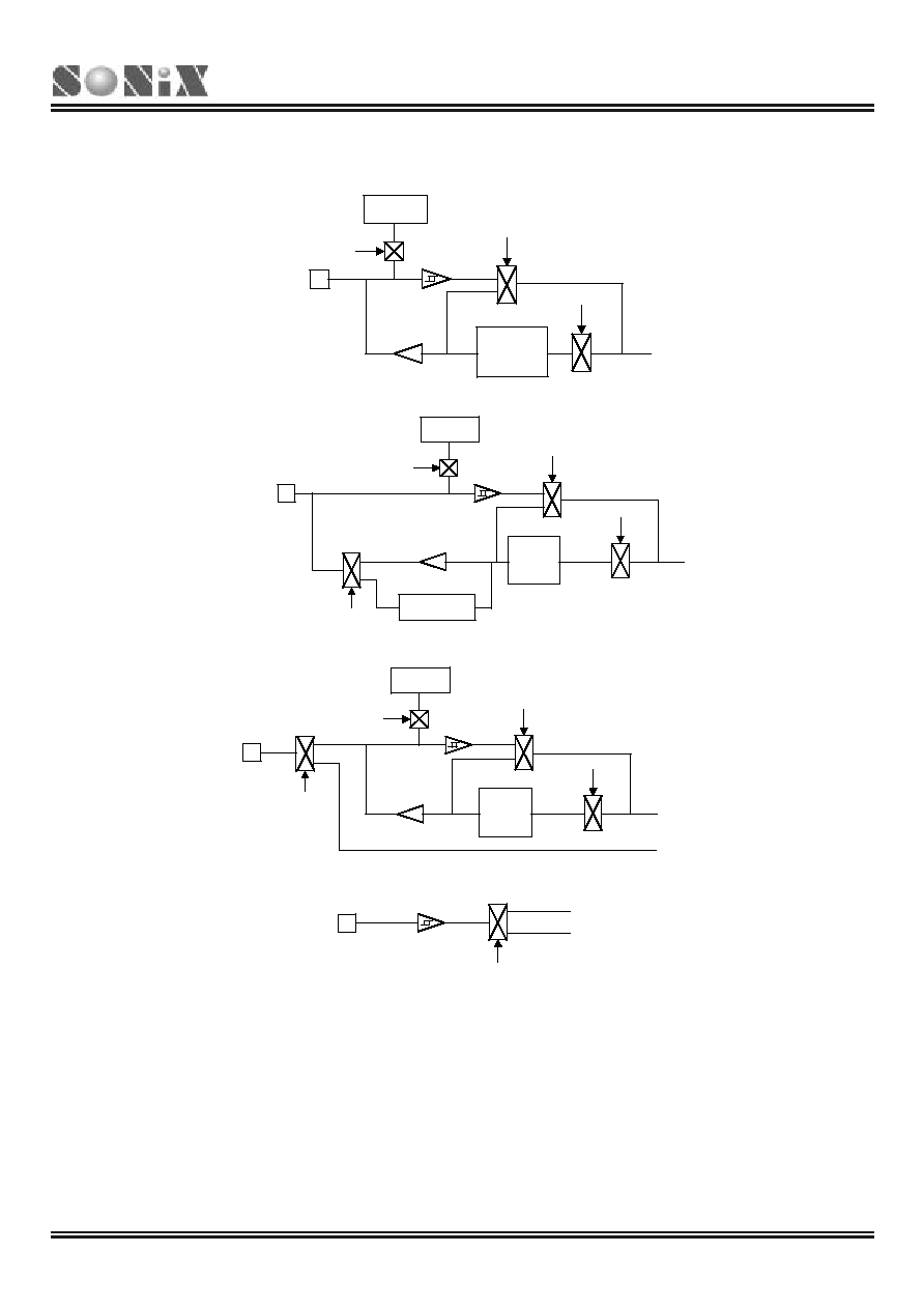
2.5 ADDRESSING
MODE
2.5.1 IMMEDIATE ADDRESSING MODE
The immediate addressing mode uses an immediate data to set up the location (" MOV A, # I ", " B0MOV M, # I ") in
ACC or specific RAM.
Example: Immediate addressing mode
MOV
A, #12H
; To set an immediate data 12H into ACC
2.5.2
2.5.3 DIRECTLY ADDRESSING MODE
The directly addressing mode moves the content of RAM location in or out of ACC.(" MOV A,12H ", " MOV 12H,
A ").
Example: Directly addressing mode
B0MOV
A, 12H
; To get a content of location 12H of bank 0 and save in ACC
2.5.4
2.5.5 INDIRECTLY ADDRESSING MODE
The indirectly addressing mode is to access the memory by the data pointer registers (Y/Z).
Example: Indirectly addressing mode with @YZ register
CLR
Y
; To clear Y register to access RAM bank 0.
B0MOV
Z, #12H
; To set an immediate data 12H into Z register.
B0MOV
A, @YZ
; Use data pointer @YZ reads a data from RAM location
; 012H into ACC.

SN8P2501A
8-Bit Micro-Controller
SONiX TECHNOLOGY CO., LTD
Page 27
Preliminary Version 0.2
2.6 STACK
OPERATIONS
2.6.1 OVERVIEW
The stack buffer of SN8P Series MCU has 4-level. These buffers are designed to push and pop up program counter's
(PC) data when interrupt service routine is executed. The STKP register is a pointer designed to point active level in
order to push or pop up data from stack buffer. The STKnH and STKnL are the stack buffers to store program counter
(PC) data.
STKP = 0
STKP = 1
STKP = 2
STKP = 3
STKP -1
STKP + 1
CALL /
interrupt
RET /
RETI
STKP
PCH
PCL
STKP
STK0H
STK1H
STK2H
STK3H
STK0L
STK1L
STK2L
STK3L
STKP = 0
STKP = 1
STKP = 2
STKP = 3
STKP = 0
STKP = 1
STKP = 2
STKP = 3
STKP -1
STKP + 1
CALL /
interrupt
RET /
RETI
STKP -1
STKP + 1
STKP -1
STKP -1
STKP + 1
CALL /
interrupt
RET /
RETI
STKP
STKP
PCH
PCL
PCH
PCH
PCL
PCL
STKP
STKP
STK0H
STK1H
STK2H
STK3H
STK0L
STK1L
STK2L
STK3L
SN8P2501A
8-Bit Micro-Controller
SONiX TECHNOLOGY CO., LTD
Page 28
Preliminary Version 0.2
2.6.2 STACK REGISTERS
The stack pointer (STKP) is a 3-bit register to store the address used to access the stack buffer, 10-bit data memory
(STKnH and STKnL) set aside for temporary storage of stack addresses.
The two stack operations are writing to the top of the stack (push) and reading from the top of stack (pop). Push
operation decrements the STKP and the pop operation increments each time. That makes the STKP always point to
the top address of stack buffer and write the last program counter value (PC) into the stack buffer.
The program counter (PC) value is stored in the stack buffer before a CALL instruction executed or during interrupt
service routine. Stack operation is a LIFO type (Last in and first out). The stack pointer (STKP) and stack buffer
(STKnH and STKnL) are located in the system register area bank 0.
0DFH
Bit 7
Bit 6
Bit 5
Bit 4
Bit 3
Bit 2
Bit 1
Bit 0
STKP
GIE
- - - -
STKPB2
STKPB1
STKPB0
Read/Write
R/W
- - - -
R/W
R/W
R/W
After
reset
0 - - - - 1 1 1
STKPBn: Stack pointer (n = 0 ~ 2)
GIE: Global interrupt control bit. 0 = disable, 1 = enable. Please refer to the interrupt chapter.
Example: Stack pointer (STKP) reset, we strongly recommended to clear the stack pointers in the
beginning of the program.
MOV
A,
#00000111B
B0MOV
STKP,
A
0F0H~0FFH
Bit 7
Bit 6
Bit 5
Bit 4
Bit 3
Bit 2
Bit 1
Bit 0
STKnH
- - - - - -
SnPC9
SnPC8
Read/Write
- - - - - -
R/W
R/W
After
reset
- - - - - - 0 0
STKn = <STKnH , STKnL> (n = 3 ~ 0)
0F0H~0FFH
Bit 7
Bit 6
Bit 5
Bit 4
Bit 3
Bit 2
Bit 1
Bit 0
STKnL
SnPC7 SnPC6 SnPC5 SnPC4 SnPC3 SnPC2 SnPC1 SnPC0
Read/Write R/W
R/W
R/W R/W R/W R/W R/W R/W
After
reset
0 0 0 0 0 0 0 0
For SN8P2501A : STKn = <STKnH , STKnL> (n = 3 ~ 0)
SN8P2501A
8-Bit Micro-Controller
SONiX TECHNOLOGY CO., LTD
Page 29
Preliminary Version 0.2
2.6.3 STACK OPERATION EXAMPLE
The two kinds of Stack-Save operations refer to the stack pointer (STKP) and write the content of program counter (PC)
to the stack buffer are CALL instruction and interrupt service. Under each condition, the STKP decreases and points to
the next available stack location. The stack buffer stores the program counter about the op-code address. The
Stack-Save operation is as the following table.
STKP Register
Stack Buffer
Stack Level
STKPB2 STKPB1 STKPB0 High
Byte
Low
Byte
Description
0
1 1 1
Free
Free
-
1
1 1 0
STK0H
STK0L
-
2
1 0 1
STK1H
STK1L
-
3
1 0 0
STK2H
STK2L
-
4
0 1 1
STK3H
STK3L
-
> 4
0 1 0 - -
Stack Over, error
There are Stack-Restore operations correspond to each push operation to restore the program counter (PC). The RETI
instruction uses for interrupt service routine. The RET instruction is for CALL instruction. When a pop operation occurs,
the STKP is incremented and points to the next free stack location. The stack buffer restores the last program counter
(PC) to the program counter registers. The Stack-Restore operation is as the following table.
STKP Register
Stack Buffer
Stack Level
STKPB2 STKPB1 STKPB0 High
Byte
Low
Byte
Description
4
0 1 1
STK3H
STK3L
-
3
1 0 0
STK2H
STK2L
-
2
1 0 1
STK1H
STK1L
-
1
1 1 0
STK0H
STK0L
-
0
1 1 1
Free
Free
-
SN8P2501A
8-Bit Micro-Controller
SONiX TECHNOLOGY CO., LTD
Page 30
Preliminary Version 0.2
3
3
3
RESET
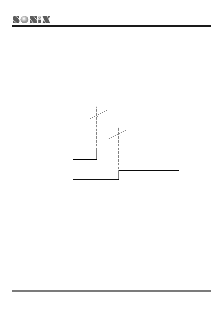
3.1 OVERVIEW
This MCU provides two system resets. One is external reset and the other is internal low voltage detector (LVD). The
external reset is a simple RC circuit connecting to the reset pin. The low voltage detector (LVD) is built-in internal circuit.
When one of the reset is triggered then will reset MCU and system registers become initial value. The timing diagram is
as the following.
VDD
External Reset
Internal Reset Signal
End of LVD Reset
LVD
End of External Reset
LVD Detect Level
External Reset Detect Level
Power on reset timing diagram
SN8P2501A
8-Bit Micro-Controller
SONiX TECHNOLOGY CO., LTD
Page 31
Preliminary Version 0.2
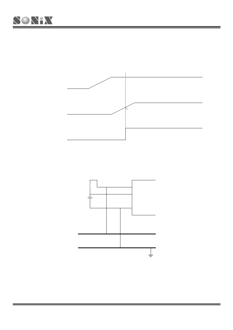
3.2 EXTERNAL RESET DESCRIPTION
The external reset is a low level active device. The reset pin receives the low voltage and resets the system. When the
voltage detects high level, it stops resetting the system. Users can use an external reset circuit to control system
operation.
External Reset
VDD
Internal Reset Signal
External Reset Detect Level
End of External Reset
System Reset
Users must make sure the VDD is stable earlier than external reset. Otherwise, the power on reset maybe fail.
The external reset circuit is a simple RC circuit as the following figure.
GND
VCC
RST
VDD
MCU
VSS
R
20K ohm
C
0.1uF
SN8P2501A
8-Bit Micro-Controller
SONiX TECHNOLOGY CO., LTD
Page 32
Preliminary Version 0.2
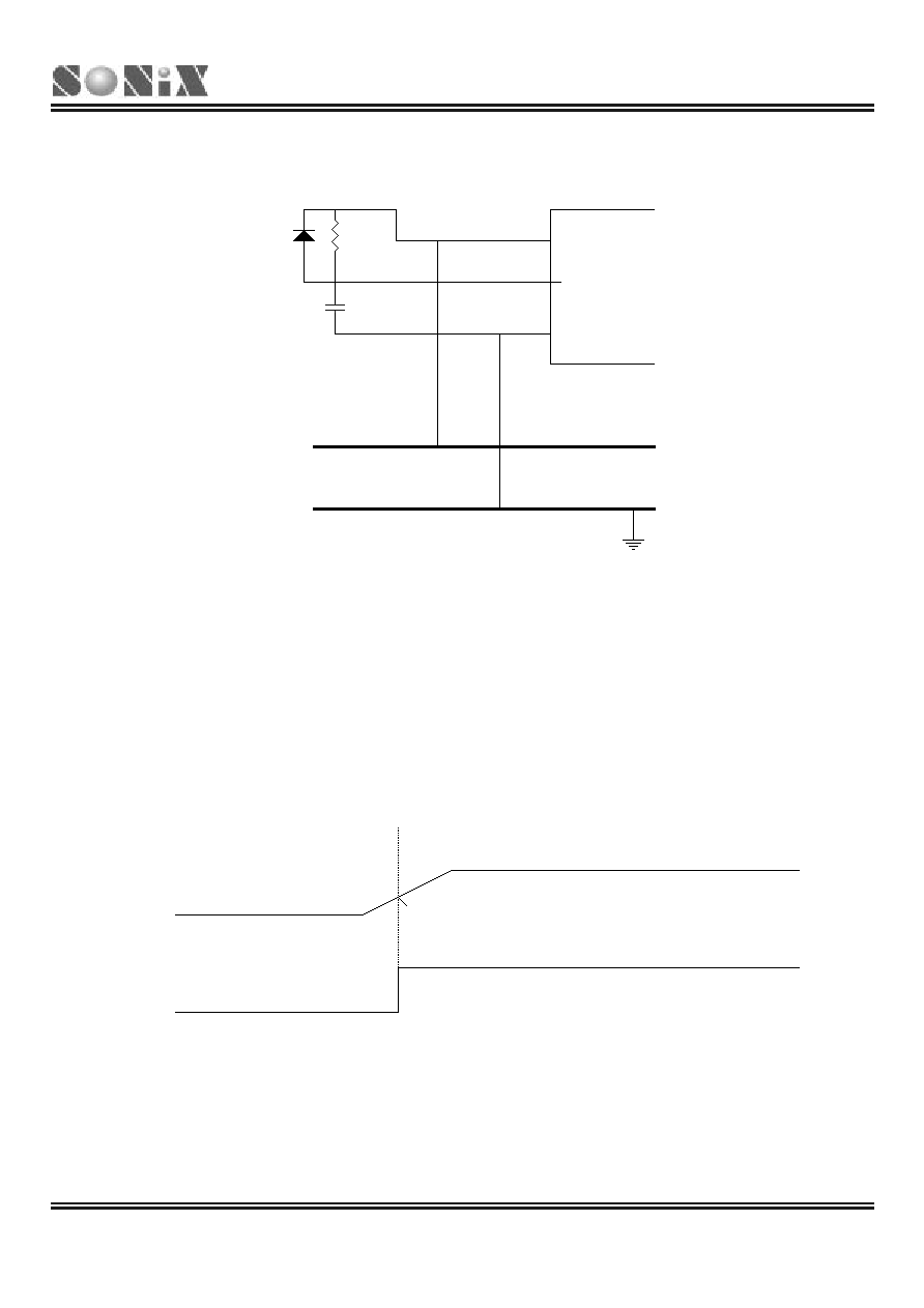
Under different environment, by placing a diode in between VCC and reset pin will help the Brownout reset.
GND
VCC
RST
VDD
MCU
VSS
R
20K ohm
C
0.1uF
DIODE
3.3 LOW VOLTAGE DETECTOR (LVD) DESCRIPTION
The LVD is a low voltage detector. It detects VDD level and reset the system as the VDD lower than the detected
voltage. The detect level is 1.8V. If the VDD lower than 1.8V, the system resets.
System Reset
LVD Detect Level
End of LVD Reset
VDD
LVD
SN8P2501A
8-Bit Micro-Controller
SONiX TECHNOLOGY CO., LTD
Page 33
Preliminary Version 0.2
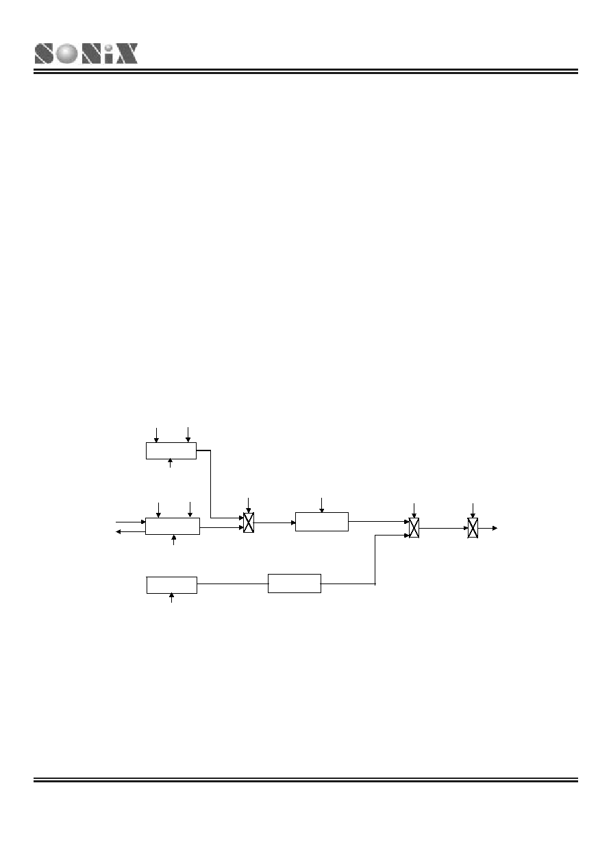
4
4
4
OSCILLATOR AND SYSTEM CLOCK
4.1 OVERVIEW
The SN8P2501A is a dual clock micro-controller system. There are high-speed clock and low-speed clock. The
high-speed clock is generated from the external oscillator circuit or on-chip 16MHz high-speed RC oscillator circuit
(IHRC 16MHz). The low-speed clock is generated from on-chip low-speed RC oscillator circuit (ILRC 16KHz @3V,
32KHz @5V).
Both the high-speed clock and the low-speed clock can be system clock (Fosc). The system clock is divided by 4 to be
the instruction cycle (Fcpu).
Normal Mode (High Clock):
Fcpu = Fosc / N, N = 1 ~ 64, Select N by Fcpu code option
Slow Mode (Low Clock):
Fcpu = Fosc/4
4.2 CLOCK BLOCK DIAGRAM
CPUM0
ILOSC.
CPUM0
ILOSC.
EHOSC.
XIN
CLKMD
Noise Filter Code Option
HOSC
STPHX
HOSC
STPHX
HOSC
IHOSC.
HOSC
STPHX
HOSC
STPHX
CPUM0
CPUM0
CPUM0
CPUM0
˜
1 ~ 64
Fhosc
Flosc
Fcpu
CPUM0
XOUT
˜
4
HOSC: High_Clk code option
EHOSC: External high-speed clock
IHRC: Internal high-speed RC clock
ILRC: Internal low-speed RC clock

SN8P2501A
8-Bit Micro-Controller
SONiX TECHNOLOGY CO., LTD
Page 34
Preliminary Version 0.2
4.3 OSCM
REGISTER
DESCRIPTION
The OSCM register is an oscillator control register. It controls oscillator status, system mode.
0CAH
Bit 7
Bit 6
Bit 5
Bit 4
Bit 3
Bit 2
Bit 1
Bit 0
OSCM
0 0 0
CPUM1
CPUM0
CLKMD
STPHX
0
Read/Write
-
-
- R/W R/W R/W R/W -
After
reset
- - - 0 0 0 0 -
STPHX: External high-speed oscillator control bit. 0 = free run, 1 = stop. This bit only controls external high-speed
oscillator. If STPHX=1, the internal low-speed RC oscillator is still running.
CLKMD: System high/Low clock mode: bit 0 = normal (dual) mode, 1 = slow mode.
CPUM1, CPUM0: CPU operating mode control bit:
00 = normal
01 = sleep (power down) mode
10 = green mode
11 = reserved.
Example: Stop high-speed oscillator
B0BSET
FSTPHX
; To stop external high-speed oscillator only.
Example: When entering the Power Down mode, both high-speed oscillator and internal low-speed
oscillator will be stopped.
B0BSET
FCPUM0
; To stop external high-speed oscillator and internal low-speed
; oscillator called power down mode (sleep mode).

SN8P2501A
8-Bit Micro-Controller
SONiX TECHNOLOGY CO., LTD
Page 35
Preliminary Version 0.2
4.4 EXTERNAL SYSTEM OSCILLATOR CIRCUITS
MCU
XIN
VDD
XOUT
VSS
CRYSTAL
20PF
20PF
Crystal/Ceramic Oscillator
MCU
XIN
VDD
VSS
XOUT
C
R
RC Oscillator
XIN
VDD
MCU
VSS
XOUT
External Clock Input
External clock input
Note1: The external oscillator circuit must be directly from Vss pin of micro-controller.

SN8P2501A
8-Bit Micro-Controller
SONiX TECHNOLOGY CO., LTD
Page 36
Preliminary Version 0.2
4.4.1 OSCILLATOR FREQUENCY MEASUREMENT
Under design period, the users can measure Fosc by software instruction cycle (Fcpu). This way is useful in RC mode.
Example: Fcpu instruction cycle of external oscillator
B0BSET
P1M.0
; Set P1.0 to be output mode for outputting Fcpu toggle signal.
@@:
B0BSET
P1.0
; Output Fcpu toggle signal in low-speed clock mode.
B0BCLR
P1.0
; Measure the Fcpu frequency by oscilloscope.
JMP
@B
Note: Do not measure the RC frequency directly from XIN; the probe impendence will affect the RC
value.
SN8P2501A
8-Bit Micro-Controller
SONiX TECHNOLOGY CO., LTD
Page 37
Preliminary Version 0.2
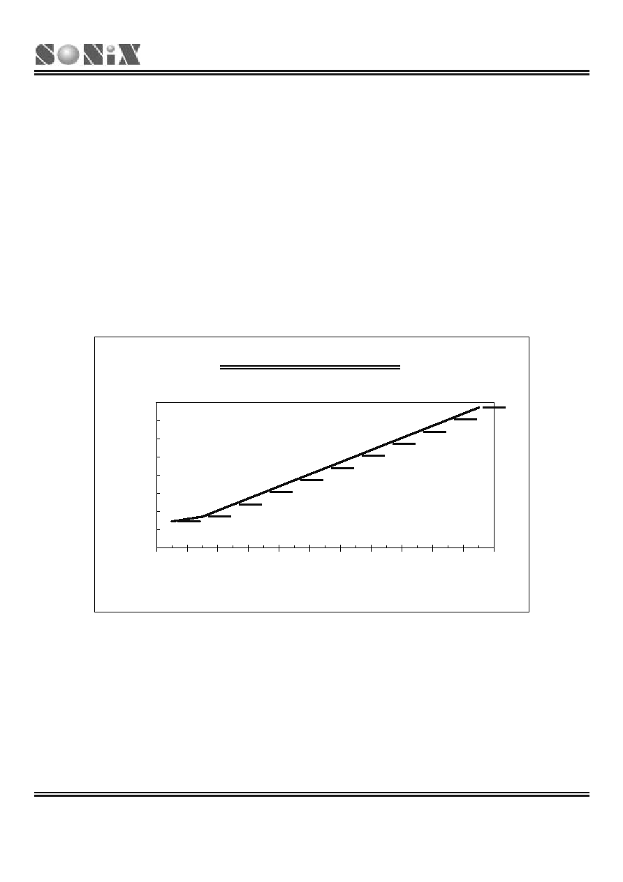
4.4.2 INTERNAL LOW-SPEED RC OSCILLATOR
The internal low-speed oscillator is built in the micro-controller. The low-speed clock source is a RC type oscillator
circuit.
Example: Stop internal low-speed oscillator
B0BSET
FCPUM0
; To stop external high-speed oscillator and internal low-speed
; oscillator called power down mode (sleep mode).
Note: The internal low-speed clock can't be turned off individually. It is controlled by CPUM0 bit of OSCM
register.
The low-speed oscillator uses RC type oscillator circuit. The frequency is affected by the voltage and temperature of
the system. In common condition, the frequency of the RC oscillator is about 16KHz at 3V and 32KHz at 5V. The
relation between the RC frequency and voltage is as the following figure.
Internal RC vs. VDD
7.329
8.663
11.998
15.333
18.668
22.003
25.338
28.673
32.008
35.343
38.678
0
5
10
15
20
25
30
35
40
1.80
2.00
2.50
3.00
3.50
4.00
4.50
5.00
5.50
6.00
6.50
VDD (Volts)
Fintrc (KHz)
Example: Measure the internal RC frequency by instruction cycle (Fcpu). The internal RC frequency is the
Fcpu multiplied by 4. We can get the Fosc frequency of internal RC from the Fcpu frequency.
B0BSET
P1M.0
; Set P1.0 to be output mode for outputting Fcpu toggle signal.
B0BSET
FCLKMD
; Switch the system clock to internal low-speed clock mode.
@@:
B0BSET
P1.0
; Output Fcpu toggle signal in low-speed clock mode.
B0BCLR
P1.0
; Measure the Fcpu frequency by oscilloscope.
JMP
@B

SN8P2501A
8-Bit Micro-Controller
SONiX TECHNOLOGY CO., LTD
Page 38
Preliminary Version 0.2
5
5
5
SYSTEM OPERATION MODE
5.1 OVERVIEW
The chip is featured with low power consumption by switching around four different modes as following.
High-speed mode
Low-speed mode
Power-down mode (Sleep mode)
Green mode
5.2 NORMAL
MODE
In normal mode, the system clock source is high clock (external or internal 16MHz RC oscillator). After power on reset,
watchdog reset, LVD reset or wakeup from power down mode, the system works under normal mode. From normal
mode, the system can get into power down mode, slow mode and green mode.
5.3 SLOW
MODE
In slow mode, the system clock source is internal low-speed RC clock. To set CLKMD =1, the system switches into
slow mode. In slow mode, the system functions similar to the normal mode except using the internal low RC clock. The
system in slow mode can switch back to high-speed normal mode. On the other hand, it can be easily switch to power
down mode and green mode for less power consumption.
5.4 GREEN
MODE
The green mode provides a time-variable wakeup function. Users can decide wakeup time by setting T0 timer. There
are two paths into green mode. One is from normal mode and the other is from slow mode. The system can be waked
up to last system mode by T0 timer timeout or P0, P1 level change trigger signal.
5.5 POWER
DOWN
MODE
The power down mode is also called sleep mode. The MCU stops working as sleeping status. To set CUPM0 = 1, the
system gets into power down mode. The external high-speed and low-speed oscillators are turned off. The system can
be waked up by P0, P1 level change trigger signal.
SN8P2501A
8-Bit Micro-Controller
SONiX TECHNOLOGY CO., LTD
Page 39
Preliminary Version 0.2
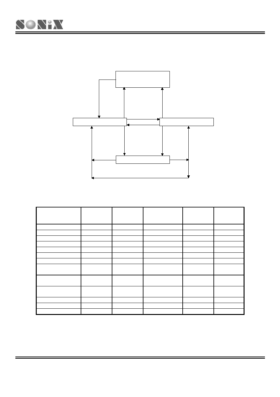
5.6 SYSTEM MODE CONTROL
System Mode Switching Diagram
Operating mode description
MODE NORMAL
SLOW GREEN
POWER
DOWN
(SLEEP)
REMARK
EHOSC
Running
By STPHX
By STPHX
Stop
IHRC
Running
By STPHX
By STPHX
Stop
ILRC Running
Running
Running Stop
EHOSC with RTC Running By
STPHX
Running
Stop
IHRC with RTC Running By
STPHX
Stop
Stop
ILRC with RTC Running Running
Stop
Stop
CPU instruction
Executing Executing
Stop
Stop
T0 timer
*Active
*Active *Active Inactive
* Active by
program
TC0 timer
*Active
*Active
Inactive
Inactive
* Active by
program
Watchdog timer
By watchdog
code option
By watchdog
code option
By watchdog
code option
By watchdog
code option
Internal interrupt
All active
All active
T0
All inactive
External interrupt
All active
All active
All active
All inactive
Wakeup source
-
-
P0, P1, T0 Reset P0, P1, Reset
Normal Mode
Green Mode
Slow Mode
Power Down Mode
(Sleep Mode)
P0, P1 wake-up function active.
External reset circuit active.
CPUM1, CPUM0 = 01
CLKMD = 0
CLKMD = 1
CPUM1, CPUM0 = 10
P0, P1 wake-up function active.
TC0 time out.
P0, P1 wake-up function active.
TC0 time out.
External reset circuit active.
External reset circuit active.

SN8P2501A
8-Bit Micro-Controller
SONiX TECHNOLOGY CO., LTD
Page 40
Preliminary Version 0.2
5.6.1 SYSTEM MODE SWITCHING
Switch normal/slow mode to power down (sleep) mode.
B0BSET
FCPUM0
; Set CPUM0 = 1.
During the sleep, only the wakeup pin and reset can wakeup the system back to the normal mode.
Switch normal mode to slow mode.
B0BSET
FCLKMD
;To set CLKMD = 1, Change the system into slow mode
B0BSET
FSTPHX
;To stop external high-speed oscillator for power saving.
Switch slow mode to normal mode (The external high-speed oscillator is still running)
B0BCLR
FCLKMD
;To set CLKMD = 0
Switch slow mode to normal mode (The external high-speed oscillator stops)
If external high clock stop and program want to switch back normal mode. It is necessary to delay at least 10mS for
external clock stable.
B0BCLR
FSTPHX
; Turn on the external high-speed oscillator.
B0MOV
Z, #27
; If VDD = 5V, internal RC=32KHz (typical) will delay
@@:
DECMS
Z
; 0.125ms X 81 = 10.125ms for external clock stable
JMP
@B
;
B0BCLR
FCLKMD
; Change the system back to the normal mode
Switch normal/slow mode to green mode.
B0BSET
FCPUM1
; Set CPUM1 = 1.
During the green mode without T0 wake-up function, only the wakeup pin wakeup the system back to the
last mode.
SN8P2501A
8-Bit Micro-Controller
SONiX TECHNOLOGY CO., LTD
Page 41
Preliminary Version 0.2
Switch normal/slow mode to green mode and enable T0 wake-up function.
; Set T0 timer wakeup function.
B0BCLR
FT0IEN
; To disable T0 interrupt service
B0BCLR
FT0ENB
; To disable T0 timer
MOV
A,#20H
;
B0MOV
T0M,A
; To set T0 clock = Fcpu / 64
MOV
A,#74H
B0MOV
T0C,A
; To set T0C initial value = 74H (To set T0 interval = 10 ms)
B0BCLR
FT0IEN
; To disable T0 interrupt service
B0BCLR
FT0IRQ
; To clear T0 interrupt request
B0BSET
FT0ENB
; To enable T0 timer
; Go into green mode
B0BCLR
FCPUM0
;To set CPUMx = 10
B0BSET
FCPUM1
During the green mode with T0 wake-up function, the wakeup pin and T0 wakeup the system back to the
last mode. T0 wake-up period is controlled by program.
Switch normal/slow mode to green mode and enable T0 wake-up function with RTC.
; Set T0 timer wakeup function with 0.5 sec RTC.
B0BCLR
FRTC1
; Set RTC timer period to 0.5 sec.
B0BCLR FRTC0
B0BSET
FT0ENB
; To enable T0 timer
B0BSET
FT0TB
; To enable RTC function
; Go into green mode
B0BCLR
FCPUM0
;To set CPUMx = 10
B0BSET
FCPUM1
During the green mode with T0 RTC wake-up function, the wakeup pin and T0 wakeup the system back to
the last mode. The T0 wake-up period is controlled by OPTION register.
088H
Bit 7
Bit 6
Bit 5
Bit 4
Bit 3
Bit 2
Bit 1
Bit 0
OPTION
- - - -
RTC1
RTC0
- -
Read/Write
- - - -
R/W
R/W
- -
After reset
- - - - 0 0 - -
RTC1, RTC0: 00 = 0.5 sec. 01 = 1 sec. 10 = 2 sec. 11 = 4 sec.

SN8P2501A
8-Bit Micro-Controller
SONiX TECHNOLOGY CO., LTD
Page 42
Preliminary Version 0.2
5.7 WAKEUP
5.7.1 OVERVIEW
The high clock (external or internal 16MHz RC oscillator) needs a delay time from stopping to operating. The delay is
necessary for oscillator to be stabilized The delay time for high clock oscillator restart is sometimes called wakeup time.
Following are two conditions require wakeup time, one is switching power down mode to normal mode, and the other is
switching slow mode to normal mode. For the first condition, MCU provides 2048 oscillator clocks as the wakeup time.
The second condition, users need to take the wakeup time into consideration, which involved stabilizing period for start
up the external high-speed oscillator.
Under power down mode (sleep mode) or green mode, P0 and P1 with wakeup function are able to wake the system
up. Port 0 wakeup function always enables, but the Port 1 is controlled by the P1W register. The wakeup signal is level
change trigger.
5.7.2 WAKEUP TIME
When the system is in power down mode (sleep mode), the high clock oscillator stops. When waked up from power
down mode, MCU waits for 2048 external high-speed oscillator clocks as the wakeup time to stable the oscillator circuit.
After the wakeup time, the system goes into the normal mode. The value of the wakeup time is as the following.
The Wakeup time = 1/Fosc * 2048 (sec) + X'tal settling time
The X'tal settling time is depended on the X'tal type. Typically, it is about 2~4mS in 4MHz Crystal oscillator
5.7.3 P1W WAKEUP CONTROL REGISTER
Under power down mode (sleep mode) or green mode, P0 and P1 with wakeup function are able to wakeup the system
Port 0 wakeup function is always available, but the Port 1 is controlled by the P1W register. The wakeup signal is level
change trigger.
0C0H
Bit 7
Bit 6
Bit 5
Bit 4
Bit 3
Bit 2
Bit 1
Bit 0
P1W
- - - -
P13W
P12W
P11W
P10W
Read/Write
- - - - W
W
W
W
After reset
- - - - 0 0 0 0
P10W~P13W: Port 1 wakeup function control bits. 0 = Disable; 1 = Enable wakeup function.

SN8P2501A
8-Bit Micro-Controller
SONiX TECHNOLOGY CO., LTD
Page 43
Preliminary Version 0.2
6
6
6
INTERRUPT
6.1 OVERVIEW
This MCU provides three interrupt sources, including two internal interrupt (T0/TC0) and one external interrupt (INT0).
The external interrupt can wakeup the chip while the system is switched from power down mode to high-speed normal
mode. Once interrupt service is executed, the GIE bit in STKP register will clear to "0" for stopping other interrupt
request. On the contrast, when interrupt service exits, the GIE bit will set to "1" to accept the next interrupts' request. All
of the interrupt request signals are stored in INTRQ register.
Note: The GIE bit must enable during all interrupt operation.
6.2 INTEN INTERRUPT ENABLE REGISTER
INTEN is the interrupt request control register including one internal interrupts, one external interrupts enable control
bits. One of the register to be set "1" is to enable the interrupt request function. Once of the interrupt occur, the stack is
incremented and program jump to ORG 8 to execute interrupt service routines. The program exits the interrupt service
routine when the returning interrupt service routine instruction (RETI) is executed.
0C9H
Bit 7
Bit 6
Bit 5
Bit 4
Bit 3
Bit 2
Bit 1
Bit 0
INTEN
- -
TC0IEN
T0IEN
- - -
P00IEN
Read/Write
- -
R/W
R/W
- - -
R/W
After reset
- - 0 0 - - - 0
P00IEN : External P0.0 interrupt control bit. 0 = disable, 1 = enable.
T0IEN : T0 Timer interrupt control bit 0 = disable, 1 = enable.
TC0IEN : TC0 Timer interrupt control bit 0 = disable, 1 = enable.
INTRQ
3-bit
Latchs
T0IRQ
TC0IRQ
P00IRQ
Interrupt
enable
gating
Global interrupt request signal
Interrupt vector address (0008H)
T0 time out
TC0 time out
INTEN Interrupt enable register
INT0 trigger
INTRQ
3-bit
Latchs
T0IRQ
TC0IRQ
P00IRQ
Interrupt
enable
gating
Global interrupt request signal
Interrupt vector address (0008H)
T0 time out
TC0 time out
INTEN Interrupt enable register
INT0 trigger
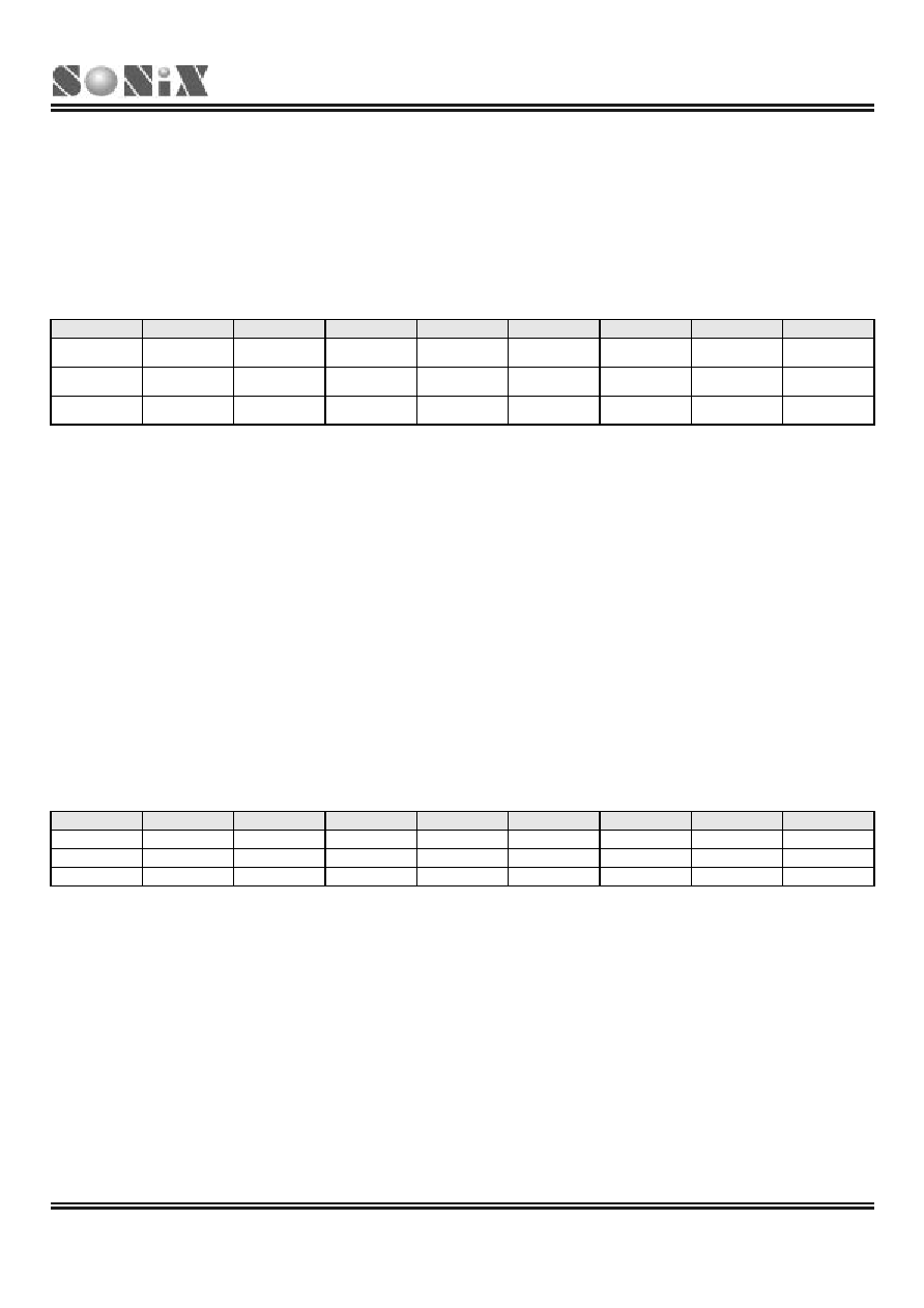
SN8P2501A
8-Bit Micro-Controller
SONiX TECHNOLOGY CO., LTD
Page 44
Preliminary Version 0.2
6.3 INTRQ INTERRUPT REQUEST REGISTER
INTRQ is the interrupt request flag register. The register includes all interrupt request indication flags. Each one of the
interrupt requests occurs, the bit of the INTRQ register would be set "1". The INTRQ value needs to be clear by
programming after detecting the flag. In the interrupt vector of program, users know the any interrupt requests
occurring by the register and do the routine corresponding of the interrupt request.
0C8H
Bit 7
Bit 6
Bit 5
Bit 4
Bit 3
Bit 2
Bit 1
Bit 0
INTRQ
- -
TC0IRQ
T0IRQ
- - -
P00IRQ
Read/Write
- -
R/W
R/W
- - -
R/W
After reset
- - 0 0 - - - 0
P00IRQ : External P0.0 interrupt request bit. 0 = non-request, 1 = request.
T0IRQ : T0 timer interrupt request controls bit 0 = non request, 1 = request.
TC0IRQ : TC0 timer interrupt request controls bit 0 = non request, 1 = request.
6.4 INTERRUPT OPERATION DESCRIPTION
6.4.1 GIE GLOBAL INTERRUPT OPERATION
GIE is the global interrupt control bit. All interrupts start work after the GIE = 1. It is necessary for interrupt service
request. One of the interrupt requests occurs, and the program counter (PC) points to the interrupt vector (ORG 8) and
the stack add 1 level.
0DFH
Bit 7
Bit 6
Bit 5
Bit 4
Bit 3
Bit 2
Bit 1
Bit 0
STKP
GIE
- - - -
STKPB2
STKPB1
STKPB0
Read/Write
R/W
- - - -
R/W
R/W
R/W
After
reset
0 - - - - 1 1 1
GIE: Global interrupt control bit. 0 = disable, 1 = enable.
Example: Set global interrupt control bit (GIE).
B0BSET
FGIE
; Enable GIE
Note: The GIE bit must enable during all interrupt operation.

SN8P2501A
8-Bit Micro-Controller
SONiX TECHNOLOGY CO., LTD
Page 45
Preliminary Version 0.2
6.4.2 INT0 (P0.0) INTERRUPT OPERATION
The interrupt trigger direction is control by PEDGE register.
0BFH
Bit 7
Bit 6
Bit 5
Bit 4
Bit 3
Bit 2
Bit 1
Bit 0
PEDGE
-
-
- P00G1
P00G0 -
-
-
Read/Write
- - -
R/W
R/W
- - -
After
reset
- - - 1 0 - - -
P00G[1:0]: P0.0 interrupt trigger edge control bits.
00 = reserved
01 = rising edge
10 = falling edge
11 = rising/falling bi-direction (Level change trigger).
Example: INT0 interrupt request setup.
B0BSET
FP00IEN
;
Enable
INT0 interrupt service
B0BCLR
FP00IRQ
; Clear INT0 interrupt request flag
B0BSET
FGIE
; Enable GIE
Example: INT0 interrupt service routine.
ACCBUF
EQU
00H
; ACCBUF is ACC data buffer.
PFLAGBUF
EQU
01H
; PFLAGBUF is PFLAG data buffer.
ORG
8
; Interrupt vector
JMP
INT_SERVICE
INT_SERVICE:
B0XCH
A, ACCBUF
; Store ACC value.
B0MOV
A,PFLAG
B0MOV
PFLAGBUF,A
; Store PFLAG value.
B0BTS1
FP00IRQ
; Check P00IRQ
JMP
EXIT_INT
; P00IRQ = 0, exit interrupt vector
B0BCLR
FP00IRQ
; Reset P00IRQ
.
.
; INT0 interrupt service routine
. .
EXIT_INT:
B0MOV
A,PFLAGBUF
; Re-load PFLAG value.
B0MOV
PFLAG,A
B0XCH
A, ACCBUF
; Re-load ACC value.
RETI
; Exit interrupt vector
When the INT0 trigger occurs, the P00IRQ will be set to "1" no matter the P00IEN is enable or disable. If the P00IEN =
1 and the trigger event P00IRQ is also set to be "1". As the result, the system will execute the interrupt vector (ORG
8). If the P00IEN = 0 and the trigger event P00IRQ is still set to be "1". Moreover, the system won't execute interrupt
vector even when the P00IRQ is set to be "1". Users need to be cautious with the operation under multi-interrupt
situation.

SN8P2501A
8-Bit Micro-Controller
SONiX TECHNOLOGY CO., LTD
Page 46
Preliminary Version 0.2
6.4.3 T0 INTERRUPT OPERATION
When the T0C counter occurs overflow, the T0IRQ will be set to "1" however the T0IEN is enable or disable. If the
T0IEN = 1, the trigger event will make the T0IRQ to be "1" and the system enter interrupt vector. If the T0IEN = 0, the
trigger event will make the T0IRQ to be "1" but the system will not enter interrupt vector. Users need to care for the
operation under multi-interrupt situation.
Example: T0 interrupt request setup.
B0BCLR
FT0IEN
; Disable T0 interrupt service
B0BCLR
FT0ENB
; Disable T0 timer
MOV
A,
#20H
;
B0MOV
T0M, A
; Set T0 clock = Fcpu / 64
MOV
A, #74H
; Set T0C initial value = 74H
B0MOV
T0C, A
; Set T0 interval = 10 ms
B0BSET
FT0IEN
; Enable T0 interrupt service
B0BCLR
FT0IRQ
; Clear T0 interrupt request flag
B0BSET
FT0ENB
; Enable T0 timer
B0BSET
FGIE
; Enable GIE
Example: T0 interrupt service routine.
ACCBUF
EQU
00H
; ACCBUF is ACC data buffer.
PFLAGBUF
EQU
01H
; PFLAGBUF is PFLAG data buffer.
ORG
8
; Interrupt vector
JMP
INT_SERVICE
INT_SERVICE:
B0XCH
A, ACCBUF
; Store ACC value.
B0MOV
A,PFLAG
B0MOV
PFLAGBUF,A
; Store PFLAG value.
B0BTS1
FT0IRQ
; Check T0IRQ
JMP
EXIT_INT
; T0IRQ = 0, exit interrupt vector
B0BCLR
FT0IRQ
; Reset T0IRQ
MOV
A,
#74H
B0MOV
T0C, A
; Reset T0C.
.
.
; T0 interrupt service routine
. .
EXIT_INT:
B0MOV
A,PFLAGBUF
; Re-load PFLAG value.
B0MOV
PFLAG,A
B0XCH
A, ACCBUF
; Re-load ACC value.
RETI
; Exit interrupt vector
When the T0C counter overflows, the T0IRQ will be set to "1" no matter the T0IEN is enable or disable. If the T0IEN
and the trigger event T0IRQ is set to be "1". As the result, the system will execute the interrupt vector. If the T0IEN =
0, the trigger event T0IRQ is still set to be "1". Moreover, the system won't execute interrupt vector even when the
T0IEN is set to be "1". Users need to be cautious with the operation under multi-interrupt situation.

SN8P2501A
8-Bit Micro-Controller
SONiX TECHNOLOGY CO., LTD
Page 47
Preliminary Version 0.2
6.4.4 TC0 INTERRUPT OPERATION
Example: TC0 interrupt request setup.
B0BCLR
FTC0IEN
; Disable TC0 interrupt service
B0BCLR
FTC0ENB
; Disable TC0 timer
MOV
A,
#20H
;
B0MOV
TC0M, A
; Set TC0 clock = Fcpu / 64
MOV
A, #74H
; Set TC0C initial value = 74H
B0MOV
TC0C, A
; Set TC0 interval = 10 ms
B0BSET
FTC0IEN
; Enable TC0 interrupt service
B0BCLR
FTC0IRQ
; Clear TC0 interrupt request flag
B0BSET
FTC0ENB
; Enable TC0 timer
B0BSET
FGIE
; Enable GIE
Example: TC0 interrupt service routine.
ACCBUF
EQU
00H
; ACCBUF is ACC data buffer.
PFLAGBUF
EQU
01H
; PFLAGBUF is PFLAG data buffer.
ORG
8
; Interrupt vector
JMP
INT_SERVICE
INT_SERVICE:
B0XCH
A, ACCBUF
; Store ACC value.
B0MOV
A,PFLAG
B0MOV
PFLAGBUF,A
; Store PFLAG value.
B0BTS1
FTC0IRQ
; Check TC0IRQ
JMP
EXIT_INT
; TC0IRQ = 0, exit interrupt vector
B0BCLR
FTC0IRQ
; Reset TC0IRQ
MOV
A,
#74H
B0MOV
TC0C, A
; Reset TC0C.
.
.
; TC0 interrupt service routine
. .
EXIT_INT:
B0MOV
A,PFLAGBUF
; Re-load PFLAG value.
B0MOV
PFLAG,A
B0XCH
A, ACCBUF
; Re-load ACC value.
RETI
; Exit interrupt vector
When the TC0C counter overflows, the TC0IRQ will be set to "1" no matter the TC0IEN is enable or disable. If the
TC0IEN and the trigger event TC0IRQ is set to be "1". As the result, the system will execute the interrupt vector. If the
TC0IEN = 0, the trigger event TC0IRQ is still set to be "1". Moreover, the system won't execute interrupt vector even
when the TC0IEN is set to be "1". Users need to be cautious with the operation under multi-interrupt situation.

SN8P2501A
8-Bit Micro-Controller
SONiX TECHNOLOGY CO., LTD
Page 48
Preliminary Version 0.2
6.4.5 MULTI-INTERRUPT OPERATION
Under certain condition, the software designer uses more than one interrupt requests. Processing multi-interrupt
request requires setting the priority of the interrupt requests. The IRQ flags of interrupts are controlled by the interrupt
event. Nevertheless, the IRQ flag "1" doesn't mean the system will execute the interrupt vector. In addition, which
means the IRQ flags can be set "1" by the events without enable the interrupt. Once the event occurs, the IRQ will be
logic "1". The IRQ and its trigger event relationship is as the below table.
Interrupt Name
Trigger Event Description
P00IRQ
P0.0 trigger controlled by PEDGE
T0IRQ T0C
overflow
TC0IRQ TC0C
overflow
For multi-interrupt conditions, two things need to be taking care of. One is to set the priority for these interrupt requests.
Two is using IEN and IRQ flags to decide which interrupt to be executed. Users have to check interrupt control bit and
interrupt request flag in interrupt routine.
Example: Check the interrupt request under multi-interrupt operation
ACCBUF
EQU
00H
; ACCBUF is ACC data buffer.
PFLAGBUF
EQU
01H
; PFLAGBUF is PFLAG data buffer.
ORG
8
; Interrupt vector
B0XCH
A, ACCBUF
; Store ACC value.
B0MOV
A,PFLAG
B0MOV
PFLAGBUF,A
; Store PFLAG value.
INTP00CHK:
; Check INT0 interrupt request
B0BTS1
FP00IEN
; Check P00IEN
JMP
INTTC0CHK
; Jump check to next interrupt
B0BTS0
FP00IRQ
; Check P00IRQ
JMP
INTP00
; Jump to INT0 interrupt service routine
INTTC0CHK:
; Check TC0 interrupt request
B0BTS1
FT0IEN
; Check T0IEN
JMP
INT_EXIT
; Jump to exit of IRQ
B0BTS0
FT0IRQ
; Check T0IRQ
JMP
INTT0
; Jump to T0 interrupt service routine
INTTC0CHK:
; Check TC0 interrupt request
B0BTS1
FTC0IEN
; Check TC0IEN
JMP
INT_EXIT
; Jump to exit of IRQ
B0BTS0
FTC0IRQ
; Check TC0IRQ
JMP
INTTC0
; Jump to TC0 interrupt service routine
INT_EXIT:
B0MOV
A,PFLAGBUF
; Re-load PFLAG value.
B0MOV
PFLAG,A
B0XCH
A, ACCBUF
; Re-load ACC value.
RETI
; Exit interrupt vector

SN8P2501A
8-Bit Micro-Controller
SONiX TECHNOLOGY CO., LTD
Page 49
Preliminary Version 0.2
7
7
7
I/O PORT
7.1 I/O PORT MODE
The port direction is programmed by PnM register. All I/O ports can select input or output direction.
0B8H
Bit 7
Bit 6
Bit 5
Bit 4
Bit 3
Bit 2
Bit 1
Bit 0
P0M
- - - - - - -
P00M
Read/Write
- - - - - - -
R/W
After
reset
- - - - - - - 0
0C1H
Bit 7
Bit 6
Bit 5
Bit 4
Bit 3
Bit 2
Bit 1
Bit 0
P1M
- - - -
P13M
P12M
-
P10M
Read/Write
- - - - R/W
R/W - R/W
After
reset
- - - - 0 0 - 0
P1.1 is input only pin, and the P1M.1 keeps "1".
0C2H
Bit 7
Bit 6
Bit 5
Bit 4
Bit 3
Bit 2
Bit 1
Bit 0
P2M
-
-
P25M P24M P23M P22M P21M P20M
Read/Write -
-
R/W R/W R/W R/W R/W R/W
After
reset
- - 0 0 0 0 0 0
0C5H
Bit 7
Bit 6
Bit 5
Bit 4
Bit 3
Bit 2
Bit 1
Bit 0
P5M
- - -
P54M
- - - -
Read/Write
- - -
R/W
- - - -
After
reset
- - - 0 - - - -
When PnM=0, the Pn is input mode
PnM=1, the Pn is output mode
Users can program them by bit control instructions (B0BSET, B0BCLR).
Example: I/O mode selecting
CLR
P0M
; Set all ports to be input mode.
CLR
P1M
CLR
P2M
CLR
P5M
MOV
A, #0FFH
; Set all ports to be output mode.
B0MOV
P0M,
A
B0MOV
P1M,
A
B0MOV
P2M,
A
B0MOV
P5M,
A
B0BCLR
P1M.2
; Set P1.2 to be input mode.
B0BSET
P1M.2
; Set P1.2 to be output mode.

SN8P2501A
8-Bit Micro-Controller
SONiX TECHNOLOGY CO., LTD
Page 50
Preliminary Version 0.2
7.2 I/O PULL UP REGISTER
0E0H
Bit 7
Bit 6
Bit 5
Bit 4
Bit 3
Bit 2
Bit 1
Bit 0
P0UR
- - - - - - -
P00R
Read/Write
- - - - - - - W
After
reset
- - - - - - - 0
0E1H
Bit 7
Bit 6
Bit 5
Bit 4
Bit 3
Bit 2
Bit 1
Bit 0
P1UR
- - - -
P13R
P12R
-
P10R
Read/Write
- - - - W
W - W
After
reset
- - - - 0 0 - 0
P1.1 is input only pin and without pull-up resister. The P1UR.1 keeps "1".
0E2H
Bit 7
Bit 6
Bit 5
Bit 4
Bit 3
Bit 2
Bit 1
Bit 0
P2UR
-
- P25R P24R P23R P22R P21R P20R
Read/Write
- - W W W W W W
After
reset
- - 0 0 0 0 0 0
0E5H
Bit 7
Bit 6
Bit 5
Bit 4
Bit 3
Bit 2
Bit 1
Bit 0
P5UR
- - -
P54R
- - - -
Read/Write
- - - W - - - -
After
reset
- - - 0 - - - -
Example: I/O Pull up Register
MOV
A, #0FFH
; Enable Port0, 1, 2, 5 Pull-up register,
B0MOV
P0UR,
A
;
B0MOV
P1UR,
A
B0MOV
P2UR,
A
B0MOV
P5UR,
A
7.3 I/O OPEN-DRAIN REGISTER
Port1
0E9H
Bit 7
Bit 6
Bit 5
Bit 4
Bit 3
Bit 2
Bit 1
Bit 0
P1OC
- - - - - - -
P10OC
Read/Write
- - - - - - - W
After
reset
- - - - - - - 0
Bit 0
P10OC: P10 open-drain control bit
0 = Disable open-drain mode
1 = Enable open-drain mode
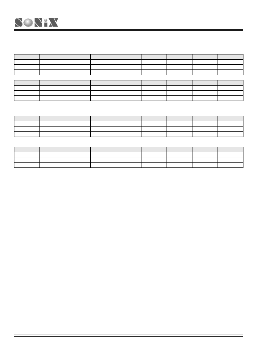
SN8P2501A
8-Bit Micro-Controller
SONiX TECHNOLOGY CO., LTD
Page 51
Preliminary Version 0.2
7.4 I/O PORT DATA REGISTER
0D0H
Bit 7
Bit 6
Bit 5
Bit 4
Bit 3
Bit 2
Bit 1
Bit 0
P0
- - - - - - -
P00
Read/Write
- - - - - - -
R/W
After
reset
- - - - - - - 0
0D1H
Bit 7
Bit 6
Bit 5
Bit 4
Bit 3
Bit 2
Bit 1
Bit 0
P1
- - - -
P13
P12
P11
P10
Read/Write
- - - -
R/W
R/W
R
R/W
After
reset
- - - - 0 0 0 0
The P11 keeps "1" when external reset enable by code option.
0D2H
Bit 7
Bit 6
Bit 5
Bit 4
Bit 3
Bit 2
Bit 1
Bit 0
P2
-
- P25 P24 P23 P22 P21 P20
Read/Write -
-
R/W R/W R/W R/W R/W R/W
After
reset
- - 0 0 0 0 0 0
0D5H
Bit 7
Bit 6
Bit 5
Bit 4
Bit 3
Bit 2
Bit 1
Bit 0
P5
- - -
P54
- - - -
Read/Write
- - -
R/W
- - - -
After
reset
- - - 0 - - - -
Example: Read data from input port.
B0MOV
A, P0
; Read data from Port 0
B0MOV
A, P1
; Read data from Port 1
B0MOV
A, P2
; Read data from Port 2
B0MOV
A, P5
; Read data from Port 5
Example: Write data to output port.
MOV
A, #0FFH
; Write data FFH to all Port.
B0MOV
P0,
A
B0MOV
P1,
A
B0MOV
P2,
A
B0MOV
P5,
A
Example: Write one bit data to output port.
B0BSET
P1.3
; Set P1.3 and P2.5 to be "1".
B0BSET
P2.5
B0BCLR
P1.3
; Set P1.3 and P2.5 to be "0".
B0BCLR
P2.5
SN8P2501A
8-Bit Micro-Controller
SONiX TECHNOLOGY CO., LTD
Page 52
Preliminary Version 0.2
8
8
8
TIMERS
8.1 WATCHDOG
TIMER
The watchdog timer (WDT) is a binary up counter designed for monitoring program execution. If the program goes into
the unknown status by noise interference, WDT overflow signal raises and resets MCU. Watchdog clock controlled by
code option and the clock source is internal low-speed oscillator (ILRC, 16K @3V, 32K @5V).
Watchdog overflow time is about 0.5 sec @3V, 0.25 sec @5V.
If watchdog is "Always_On" mode, it keeps running event under power down mode or green mode.
For S8KD ICE simulation, clear watchdog timer using "@RST_WDT" macro is necessary. Or the S8KD
watchdog would be error. Please use "@RST_WDT" macro to clear the watchdog timer successfully both
in S8KD ICE emulation and real chip.
Watchdog clear is controlled by WDTR register. Moving 0x5A data into WDTR is to reset watchdog timer.
0CCH
Bit 7
Bit 6
Bit 5
Bit 4
Bit 3
Bit 2
Bit 1
Bit 0
WDTR
WDTR7 WDTR6 WDTR5 WDTR4 WDTR3 WDTR2 WDTR1 WDTR0
Read/Write
W W W W W W W W
After
reset
0 0 0 0 0 0 0 0
Example: An operation of watchdog timer is as following. To clear the watchdog timer counter in the top
of the main routine of the program.
Main:
MOV
A,#5AH
; Clear the watchdog timer.
B0MOV WDTR,A
. .
CALL
SUB1
CALL
SUB2
. .
. .
. .
JMP
MAIN
Example: Clear watchdog timer by @RST_WDT macro.
Main:
@RST_WDT
; Clear the watchdog timer.
. .
CALL
SUB1
CALL
SUB2
. .
. .
. .
JMP
MAIN
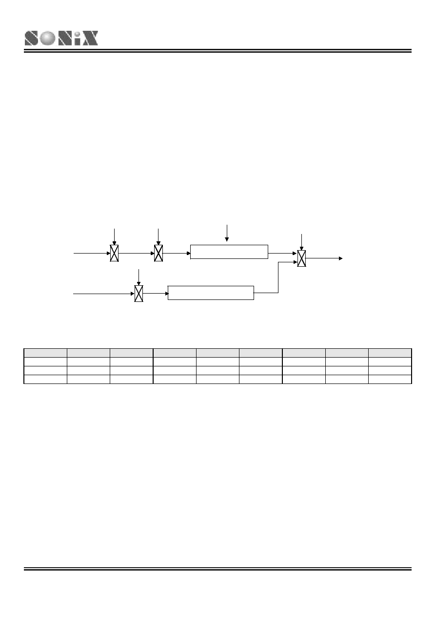
SN8P2501A
8-Bit Micro-Controller
SONiX TECHNOLOGY CO., LTD
Page 53
Preliminary Version 0.2
8.2 TIMER 0 (T0)
8.2.1 OVERVIEW
The T0 is an 8-bit binary up timer and event counter. If T0 timer occurs an overflow (from FFH to 00H), it will continue
counting and issue a time-out signal to trigger T0 interrupt to request interrupt service.
The main purposes of the T0 timer is as following.
8-bit programmable timer: Generates interrupts at specific time intervals based on the selected clock
frequency.
RTC timer: Generates interrupts at real time intervals based on the selected clock source. RTC function is
only available in High_Clk code option = "IHRC_RTC".
Green mode wakeup function: T0ENB = 1, T0 time out to make system return to last mode in green mode.
Fcpu
T0enb
T0C 8-bit binary counter
T0 Time out
pre_load
T0rate
Internal data bus
T0TB
RTC1, RTC0 period control
RTC
T0enb
Fcpu
T0enb
T0C 8-bit binary counter
T0 Time out
pre_load
T0rate
Internal data bus
T0TB
T0TB
RTC1, RTC0 period control
RTC
T0enb
T0enb
8.2.2 T0M MODE REGISTER
0D8H
Bit 7
Bit 6
Bit 5
Bit 4
Bit 3
Bit 2
Bit 1
Bit 0
T0M
T0ENB T0rate2 T0rate1 T0rate0
-
-
-
T0TB
Read/Write
R/W R/W R/W R/W -
-
- R/W
After
reset
0 0 0 0 - - - 0
T0ENB: T0 counter control bit. 0 = disable, 1 = enable.
T0RATE2~T0RATE0: T0 internal clock select bits. 000 = fcpu/256, 001 = fcpu/128, ... , 110 = fcpu/4, 111 = fcpu/2.
T0TB: RTC clock source control bit. 0 = disable (from Fcpu). 1 = enable (from RTC).

SN8P2501A
8-Bit Micro-Controller
SONiX TECHNOLOGY CO., LTD
Page 54
Preliminary Version 0.2
8.2.3 T0C COUNTING REGISTER
T0C is an 8-bit counter register for T0 interval time control.
0D9H
Bit 7
Bit 6
Bit 5
Bit 4
Bit 3
Bit 2
Bit 1
Bit 0
T0C
T0C7 T0C6 T0C5 T0C4 T0C3 T0C2 T0C1 T0C0
Read/Write R/W
R/W
R/W R/W R/W R/W R/W R/W
After
reset
0 0 0 0 0 0 0 0
The basic timer table interval time of T0
High speed mode (Fcpu = 3.58MHz / 4)
Low speed mode (Fcpu = 32768Hz / 4)
T0RATE T0CLOCK
Max overflow interval One step = max/256
Max overflow interval One step = max/256
000
fcpu/256
73.2 ms
286us
8000 ms
31.25 ms
001
fcpu/128
36.6 ms
143us
4000 ms
15.63 ms
010
fcpu/64
18.3 ms
71.5us
2000 ms
7.8 ms
011
fcpu/32
9.15 ms
35.8us
1000 ms
3.9 ms
100
fcpu/16
4.57 ms
17.9us
500 ms
1.95 ms
101
fcpu/8
2.28 ms
8.94us
250 ms
0.98 ms
110
fcpu/4
1.14 ms
4.47us
125 ms
0.49 ms
111
fcpu/2
0.57 ms
2.23us
62.5 ms
0.24 ms
The equation of T0C initial value is as following.
T0C initial value = 256 - (T0 interrupt interval time * input clock)
Example: To set 10ms interval time for T0 interrupt at 3.58MHz high-speed mode. T0C value (74H) = 256 -
(10ms * fcpu/64). Let Fcpu = Fosc / 4
T0C initial value = 256 - (T0 interrupt interval time * input clock)
= 256 - (10ms * 3.58 * 10
6
/ 4 / 64)
= 256 - (10
-2
* 3.58 * 10
6
/ 4 / 64)
= 116
= 74H

SN8P2501A
8-Bit Micro-Controller
SONiX TECHNOLOGY CO., LTD
Page 55
Preliminary Version 0.2
8.3 TIMER/COUNTER 0 (TC0)
8.3.1 OVERVIEW
The TC0 is an 8-bit binary up timer and event counter,
using TC0M register to select TC0C's clock source from Fcpu or
from external INT0 pin (falling edge trigger) for counting a precision time. If TC0 timer occurs an overflow (from FFH to
00H), it will continue counting and issue a time-out signal to trigger TC0 interrupt to request interrupt service.
The main purposes of the TC0 timer is as following.
8-bit programmable timer: Generates interrupts at specific time intervals based on the selected clock
frequency.
External event counter: Counts system "events" based on falling edge detection of external clock signals at
the INT0 input pin.
Buzzer output
PWM output
TC0R reload
data buffer
Fcpu
TC0rate
TC0enb
TC0C
8-bit binary counter
TC0 Time out
INT0
(schmitter trigger)
TC0cks
load
Aload0
Auto. reload
P5.4
˜
2
TC0out
Internal P5.4 I/O circuit
CPUM1,0
S
R
Compare
PWM0OUT
PWM
Buzzer
TC0R reload
data buffer
Fcpu
TC0rate
TC0enb
TC0C
8-bit binary counter
TC0 Time out
INT0
(schmitter trigger)
TC0cks
load
Aload0
Auto. reload
P5.4
˜
2
TC0out
Internal P5.4 I/O circuit
CPUM1,0
S
R
Compare
PWM0OUT
PWM
Buzzer
SN8P2501A
8-Bit Micro-Controller
SONiX TECHNOLOGY CO., LTD
Page 56
Preliminary Version 0.2
8.3.2 TC0M MODE REGISTER
0DAH
Bit 7
Bit 6
Bit 5
Bit 4
Bit 3
Bit 2
Bit 1
Bit 0
TC0M
TC0ENB TC0rate2 TC0rate1
TC0rate0
TC0CKS ALOAD0 TC0OUT PWM0OUT
Read/Write R/W
R/W
R/W R/W R/W R/W R/W R/W
After
reset
0 0 0 0 0 0 0 0
TC0ENB: TC0 counter control bit. 0 = disable, 1 = enable.
TC0RATE2~TC0RATE0: TC0 internal clock select bits. 000 = fcpu/256, 001 = fcpu/128, ... , 110 = fcpu/4, 111 =
fcpu/2.
TC0CKS: TC0 clock source select bit. 0 = Fcpu, 1 = External clock comes from INT0/P0.0 pin.
ALOAD0: Auto-reload control bit. 0 = disable. 1 = enable.
TC0OUT: TC0 time out toggle signal output control bit. Only valid when PWM0OUT = 0.
0 = Disable, P5.4 is I/O function.
1 = Enable, P5.4 is output TC0OUT signal.
PWM0OUT: PWM output control bit. 0 = disable. 1 = enable.
PWM duty selection table. (Only valid when PWM0OUT = 1)
ALOAD0 TC0OUT TC0 Overflow boundary PWM duty range
Max PWM
Frequency
(Fcpu = 4M)
Note
0
0
FFh to 00h
0/256 ~ 255/256
7.8125K
Overflow per 256 count
0
1
3Fh to 40h
0/64 ~ 63/64
31.25K
Overflow per 64 count
1
0
1Fh to 20h
0/32 ~ 31/32
62.5K
Overflow per 32 count
1
1
0Fh to 10h
0/16 ~ 15/16
125K
Overflow per 16 count
Note: When TC0CKS=1, TC0 became an external event counter. No more P0.0 interrupt request will be
raised. (P0.0IRQ will be always 0)
SN8P2501A
8-Bit Micro-Controller
SONiX TECHNOLOGY CO., LTD
Page 57
Preliminary Version 0.2
8.3.3 TC0C COUNTING REGISTER
TC0C is an 8-bit counter register for TC0 interval time control.
0DBH
Bit 7
Bit 6
Bit 5
Bit 4
Bit 3
Bit 2
Bit 1
Bit 0
TC0C
TC0C7 TC0C6 TC0C5 TC0C4 TC0C3 TC0C2 TC0C1 TC0C0
Read/Write R/W
R/W
R/W R/W R/W R/W R/W R/W
After
reset
0 0 0 0 0 0 0 0
The basic timer table interval time of TC0
High speed mode (Fcpu = 3.58MHz / 4)
Low speed mode (Fcpu = 32768Hz / 4)
TC0RATE TC0CLOCK
Max overflow interval One step = max/256
Max overflow interval One step = max/256
000
fcpu/256
73.2 ms
286us
8000 ms
31.25 ms
001
fcpu/128
36.6 ms
143us
4000 ms
15.63 ms
010
fcpu/64
18.3 ms
71.5us
2000 ms
7.8 ms
011
fcpu/32
9.15 ms
35.8us
1000 ms
3.9 ms
100
fcpu/16
4.57 ms
17.9us
500 ms
1.95 ms
101
fcpu/8
2.28 ms
8.94us
250 ms
0.98 ms
110
fcpu/4
1.14 ms
4.47us
125 ms
0.49 ms
111
fcpu/2
0.57 ms
2.23us
62.5 ms
0.24 ms
The equation of TC0C initial value is as following.
TC0C initial value = 256 - (TC0 interrupt interval time * input clock)
Example: To set 10ms interval time for TC0 interrupt at 3.58MHz high-speed mode. TC0C value (74H) =
256 - (10ms * fcpu/64). Let Fcpu = Fosc / 4
TC0C initial value = 256 - (TC0 interrupt interval time * input clock)
= 256 - (10ms * 3.58 * 10
6
/ 4 / 64)
= 256 - (10
-2
* 3.58 * 10
6
/ 4 / 64)
= 116
= 74H

SN8P2501A
8-Bit Micro-Controller
SONiX TECHNOLOGY CO., LTD
Page 58
Preliminary Version 0.2
8.4 BUZZER
OUTPUT
Buzzer output (TC0OUT) is from TC0 timer/counter frequency output function. By setting the TC0 clock frequency, the
clock signal is output to P5.4 and the P5.4 general purpose I/O function is auto-disable. The TC0 output signal divides
by 2. The TC0 clock has many combinations and easily to make difference frequency. The TC0OUT frequency
waveform is as following.
TC0OUT Pulse
TC0 Clock
Example: Setup TC0OUT output from TC0 to TC0OUT (P5.4). The external high-speed clock is 4MHz. The
TC0OUT frequency is 0.5KHz. Because the TC0OUT signal is divided by 2, set the TC0 clock to 1KHz. The
TC0 clock source is from external oscillator clock. T0C rate is Fcpu/4. The TC0RATE2~TC0RATE1 = 110.
TC0C = TC0R = 131.
MOV
A,#01100000B
B0MOV
TC0M,A
; Set the TC0 rate to Fcpu/4
MOV
A,#131
; Set the auto-reload reference value
B0MOV
TC0C,A
B0MOV
TC0R,A
B0BSET
FTC0OUT
; Enable TC0 output to P5.4 and disable P5.4 I/O function
B0BSET
FALOAD0
; Enable TC0 auto-reload function
B0BSET
FTC0ENB
; Enable TC0 timer

SN8P2501A
8-Bit Micro-Controller
SONiX TECHNOLOGY CO., LTD
Page 59
Preliminary Version 0.2
8.4.1 TC0OUT FREQUENCY TABLE
Fosc = 4MHz, TC0 Rate = Fcpu/8
TC0R
TC0OUT
(KHz)
TC0R
TC0OUT
(KHz)
TC0R
TC0OUT
(KHz)
TC0R
TC0OUT
(KHz)
TC0R
TC0OUT
(KHz)
0 0.2441 56 0.3125 112 0.4340 168 0.7102 224 1.9531
1 0.2451 57 0.3141 113 0.4371 169 0.7184 225 2.0161
2 0.2461 58 0.3157 114 0.4401 170 0.7267 226 2.0833
3 0.2470 59 0.3173 115 0.4433 171 0.7353 227 2.1552
4 0.2480 60 0.3189 116 0.4464 172 0.7440 228 2.2321
5 0.2490 61 0.3205 117 0.4496 173 0.7530 229 2.3148
6 0.2500 62 0.3222 118 0.4529 174 0.7622 230 2.4038
7 0.2510 63 0.3238 119 0.4562 175 0.7716 231 2.5000
8 0.2520 64 0.3255 120 0.4596 176 0.7813 232 2.6042
9 0.2530 65 0.3272 121 0.4630 177 0.7911 233 2.7174
10 0.2541 66 0.3289 122 0.4664 178 0.8013 234 2.8409
11 0.2551 67 0.3307 123 0.4699 179 0.8117 235 2.9762
12 0.2561 68 0.3324 124 0.4735 180 0.8224 236 3.1250
13 0.2572 69 0.3342 125 0.4771 181 0.8333 237 3.2895
14 0.2583 70 0.3360 126 0.4808 182 0.8446 238 3.4722
15 0.2593 71 0.3378 127 0.4845 183 0.8562 239 3.6765
16 0.2604 72 0.3397 128 0.4883 184 0.8681 240 3.9063
17 0.2615 73 0.3415 129 0.4921 185 0.8803 241 4.1667
18 0.2626 74 0.3434 130 0.4960 186 0.8929 242 4.4643
19 0.2637 75 0.3453 131 0.5000 187 0.9058 243 4.8077
20 0.2648 76 0.3472 132 0.5040 188 0.9191 244 5.2083
21 0.2660 77 0.3492 133 0.5081 189 0.9328 245 5.6818
22 0.2671 78 0.3511 134 0.5123 190 0.9470 246 6.2500
23 0.2682 79 0.3531 135 0.5165 191 0.9615 247 6.9444
24 0.2694 80 0.3551 136 0.5208 192 0.9766 248 7.8125
25 0.2706 81 0.3571 137 0.5252 193 0.9921 249 8.9286
26 0.2717 82 0.3592 138 0.5297 194 1.0081 250 10.4167
27 0.2729 83 0.3613 139 0.5342 195 1.0246 251 12.5000
28 0.2741 84 0.3634 140 0.5388 196 1.0417 252 15.6250
29 0.2753 85 0.3655 141 0.5435 197 1.0593 253 20.8333
30 0.2765 86 0.3676 142 0.5482 198 1.0776 254 31.2500
31 0.2778 87 0.3698 143 0.5531 199 1.0965 255 62.5000
32 0.2790 88 0.3720 144 0.5580 200 1.1161
33 0.2803 89 0.3743 145 0.5631 201 1.1364
34 0.2815 90 0.3765 146 0.5682 202 1.1574
35 0.2828 91 0.3788 147 0.5734 203 1.1792
36 0.2841 92 0.3811 148 0.5787 204 1.2019
37 0.2854 93 0.3834 149 0.5841 205 1.2255
38 0.2867 94 0.3858 150 0.5896 206 1.2500
39 0.2880 95 0.3882 151 0.5952 207 1.2755
40 0.2894 96 0.3906 152 0.6010 208 1.3021
41 0.2907 97 0.3931 153 0.6068 209 1.3298
42 0.2921 98 0.3956 154 0.6127 210 1.3587
43 0.2934 99 0.3981 155 0.6188 211 1.3889
44 0.2948 100 0.4006 156 0.6250 212 1.4205
45 0.2962 101 0.4032 157 0.6313 213 1.4535
46 0.2976 102 0.4058 158 0.6378 214 1.4881
47 0.2990 103 0.4085 159 0.6443 215 1.5244
48 0.3005 104 0.4112 160 0.6510 216 1.5625
49 0.3019 105 0.4139 161 0.6579 217 1.6026
50 0.3034 106 0.4167 162 0.6649 218 1.6447
51 0.3049 107 0.4195 163 0.6720 219 1.6892
52 0.3064 108 0.4223 164 0.6793 220 1.7361
53 0.3079 109 0.4252 165 0.6868 221 1.7857
54 0.3094 110 0.4281 166 0.6944 222 1.8382
55 0.3109 111 0.4310 167 0.7022 223 1.8939
SN8P2501A
8-Bit Micro-Controller
SONiX TECHNOLOGY CO., LTD
Page 60
Preliminary Version 0.2
Fosc = 16MHz, TC0 Rate = Fcpu/8
TC0R
TC0OUT
(KHz)
TC0R
TC0OUT
(KHz)
TC0R
TC0OUT
(KHz)
TC0R
TC0OUT
(KHz)
TC0R
TC0OUT
(KHz)
0 0.9766 56 1.2500 112 1.7361 168 2.8409 224 7.8125
1 0.9804 57 1.2563 113 1.7483 169 2.8736 225 8.0645
2 0.9843 58 1.2626 114 1.7606 170 2.9070 226 8.3333
3 0.9881 59 1.2690 115 1.7730 171 2.9412 227 8.6207
4 0.9921 60 1.2755 116 1.7857 172 2.9762 228 8.9286
5 0.9960 61 1.2821 117 1.7986 173 3.0120 229 9.2593
6 1.0000 62 1.2887 118 1.8116 174 3.0488 230 9.6154
7 1.0040 63 1.2953 119 1.8248 175 3.0864 231 10.0000
8 1.0081 64 1.3021 120 1.8382 176 3.1250 232 10.4167
9 1.0121 65 1.3089 121 1.8519 177 3.1646 233 10.8696
10 1.0163 66 1.3158 122 1.8657 178 3.2051 234 11.3636
11 1.0204 67 1.3228 123 1.8797 179 3.2468 235 11.9048
12 1.0246 68 1.3298 124 1.8939 180 3.2895 236 12.5000
13 1.0288 69 1.3369 125 1.9084 181 3.3333 237 13.1579
14 1.0331 70 1.3441 126 1.9231 182 3.3784 238 13.8889
15 1.0373 71 1.3514 127 1.9380 183 3.4247 239 14.7059
16 1.0417 72 1.3587 128 1.9531 184 3.4722 240 15.6250
17 1.0460 73 1.3661 129 1.9685 185 3.5211 241 16.6667
18 1.0504 74 1.3736 130 1.9841 186 3.5714 242 17.8571
19 1.0549 75 1.3812 131 2.0000 187 3.6232 243 19.2308
20 1.0593 76 1.3889 132 2.0161 188 3.6765 244 20.8333
21 1.0638 77 1.3966 133 2.0325 189 3.7313 245 22.7273
22 1.0684 78 1.4045 134 2.0492 190 3.7879 246 25.0000
23 1.0730 79 1.4124 135 2.0661 191 3.8462 247 27.7778
24 1.0776 80 1.4205 136 2.0833 192 3.9063 248 31.2500
25 1.0823 81 1.4286 137 2.1008 193 3.9683 249 35.7143
26 1.0870 82 1.4368 138 2.1186 194 4.0323 250 41.6667
27 1.0917 83 1.4451 139 2.1368 195 4.0984 251 50.0000
28 1.0965 84 1.4535 140 2.1552 196 4.1667 252 62.5000
29 1.1013 85 1.4620 141 2.1739 197 4.2373 253 83.3333
30 1.1062 86 1.4706 142 2.1930 198 4.3103 254
125.0000
31 1.1111 87 1.4793 143 2.2124 199 4.3860 255
250.0000
32 1.1161 88 1.4881 144 2.2321 200 4.4643
33 1.1211 89 1.4970 145 2.2523 201 4.5455
34 1.1261 90 1.5060 146 2.2727 202 4.6296
35 1.1312 91 1.5152 147 2.2936 203 4.7170
36 1.1364 92 1.5244 148 2.3148 204 4.8077
37 1.1416 93 1.5337 149 2.3364 205 4.9020
38 1.1468 94 1.5432 150 2.3585 206 5.0000
39 1.1521 95 1.5528 151 2.3810 207 5.1020
40 1.1574 96 1.5625 152 2.4038 208 5.2083
41 1.1628 97 1.5723 153 2.4272 209 5.3191
42 1.1682 98 1.5823 154 2.4510 210 5.4348
43 1.1737 99 1.5924 155 2.4752 211 5.5556
44 1.1792 100 1.6026 156 2.5000 212 5.6818
45 1.1848 101 1.6129 157 2.5253 213 5.8140
46 1.1905 102 1.6234 158 2.5510 214 5.9524
47 1.1962 103 1.6340 159 2.5773 215 6.0976
48 1.2019 104 1.6447 160 2.6042 216 6.2500
49 1.2077 105 1.6556 161 2.6316 217 6.4103
50 1.2136 106 1.6667 162 2.6596 218 6.5789
51 1.2195 107 1.6779 163 2.6882 219 6.7568
52 1.2255 108 1.6892 164 2.7174 220 6.9444
53 1.2315 109 1.7007 165 2.7473 221 7.1429
54 1.2376 110 1.7123 166 2.7778 222 7.3529
55 1.2438 111 1.7241 167 2.8090 223 7.5758

SN8P2501A
8-Bit Micro-Controller
SONiX TECHNOLOGY CO., LTD
Page 61
Preliminary Version 0.2
8.5 PWM FUNCTION DESCRIPTION
8.5.1 OVERVIEW
PWM function is generated by TC0 timer counter and output the PWM signal to PWM0OUT pin (P5.4). The 8-bit
counter counts modulus 256, 64, 32, 16 controlled by ALOAD0, TC0OUT bits. The value of the 8-bit counter is
compared to the contents of the reference register (TC0R). When the reference register value (TC0R) is equal to the
counter value (TC0C), the PWM output goes low. When the counter reaches zero, the PWM output is forced high. The
low-to-high ratio (duty) of the PWM0 output is TC0R/256, 64, 32, 16.
PWM output can be held at low level by continuously loading the reference register with 00H. Under PWM operating, to
change the PWM's duty cycle is to modify the TC0R.
ALOAD0 TC0OUT PWM duty range TC0C valid value TC0R valid bits value
MAX. PWM
Frequency
(Fcpu = 4MHz)
Remark
0 0
0/256~255/256
0x00~0xFF 0x00~0xFF 7.8125K
Overflow per 256 count
0 1 0/64~63/64 0x00~0x3F 0x00~0x3F
31.25K
Overflow per 64 count
1 0 0/32~31/32 0x00~0x1F 0x00~0x1F
62.5K
Overflow per 32 count
1 1 0/16~15/16 0x00~0x0F 0x00~0x0F
125K
Overflow per 16 count
The Output duty of PWM with different TC0R. Duty range is from 0/256~255/256.
TC0/TC1 Clock
TC0R/TC1R = 00H
Low
High
Low
Low
High
TC0R/TC1R = 01H
TC0R/TC1R = 80H
TC0R/TC1R = FFH
Low
High
0
1
128
..... 254 255
.....
0
1
128
..... 254 255
.....
TC0/TC1 Clock
TC0R/TC1R = 00H
Low
High
Low
Low
High
TC0R/TC1R = 01H
TC0R/TC1R = 80H
TC0R/TC1R = FFH
Low
High
Low
High
0
1
128
..... 254 255
.....
0
1
128
..... 254 255
.....
0
1
128
..... 254 255
.....
.....
0
1
128
..... 254 255
.....
.....

SN8P2501A
8-Bit Micro-Controller
SONiX TECHNOLOGY CO., LTD
Page 62
Preliminary Version 0.2
8.5.2 PWM PROGRAM DESCRIPTION
Example: Setup PWM0 output from TC0 to PWM0OUT (P5.4). The external high-speed oscillator clock is
4MHz. Fcpu = Fosc/4. The duty of PWM is 30/256. The PWM frequency is about 1KHz. The PWM clock
source is from external oscillator clock. TC0 rate is Fcpu/4. The TC0RATE2~TC0RATE1 = 110. TC0C =
TC0R = 30.
MOV
A,#01100000B
B0MOV
TC0M,A
; Set the TC0 rate to Fcpu/4
MOV
A,#30
; Set the PWM duty to 30/256
B0MOV
TC0C,A
B0MOV
TC0R,A
B0BCLR
FTC0OUT
; Set duty range as 0/256~255/256.
B0BCLR
FALOAD0
B0BSET
FPWM0OUT
; Enable PWM0 output to P5.4 and disable P5.4 I/O function
B0BSET
FTC0ENB
; Enable TC0 timer
Note: The TC0R is write-only registers. Don't process them using INCMS, DECMS instructions.
Example: Modify TC0R registers' value.
MOV
A, #30H
; Input a number using B0MOV instruction.
B0MOV
TC0R,
A
INCMS
BUF0
; Get the new TC0R value from the BUF0 buffer defined by
B0MOV
A, BUF0
; programming.
B0MOV
TC0R,
BUF0
Note: That is better to set the TC0C and TC0R value together when PWM0 duty modified. It protects the
PWM0 signal no glitch as PWM0 duty changing.
Note: The PWM can work with interrupt request.

SN8P2501A
8-Bit Micro-Controller
SONiX TECHNOLOGY CO., LTD
Page 63
Preliminary Version 0.2
9
9
9
INSTRUCTION SET TABLE
Field Mnemonic
Description
C
DC
Z
Cycle
MOV
A,M A
M
- -
1
M
MOV
M,A M
A
- - - 1
O
B0MOV A,M A
M (bank 0)
- -
1
V
B0MOV M,A M (bank 0)
A
- - - 1
E
MOV
A,I
A
I
- - - 1
B0MOV M,I M
I, (M = only for Working registers R, Y, Z , RBANK & PFLAG)
- - - 1
XCH
A,M A
M
- - - 1+N
B0XCH A,M A
M (bank 0)
- - - 1+N
MOVC
R, A
ROM [Y,Z]
- - - 2
ADC
A,M A
A + M + C, if occur carry, then C=1, else C=0
1
A
ADC
M,A M
A + M + C, if occur carry, then C=1, else C=0
1+N
R
ADD
A,M A
A + M, if occur carry, then C=1, else C=0
1
I
ADD
M,A
M
A + M, if occur carry, then C=1, else C=0
1+N
T B0ADD
M,A
M (bank 0)
M (bank 0) + A, if occur carry, then C=1, else C=0
1+N
H
ADD
A,I
A
A + I, if occur carry, then C=1, else C=0
1
M
SBC
A,M A
A - M - /C, if occur borrow, then C=0, else C=1
1
E
SBC
M,A M
A - M - /C, if occur borrow, then C=0, else C=1
1+N
T
SUB
A,M A
A - M, if occur borrow, then C=0, else C=1
1
I
SUB
M,A
M
A - M, if occur borrow, then C=0, else C=1
1+N
C
SUB
A,I
A
A - I, if occur borrow, then C=0, else C=1
1
DAA
To adjust ACC's data format from HEX to DEC.
- - 1
AND
A,M A
A and M
- -
1
L
AND
M,A M
A and M
- -
1+N
O
AND
A,I
A
A and I
- -
1
G
OR
A,M A
A or M
- -
1
I
OR
M,A M
A or M
- -
1+N
C
OR
A,I
A
A or I
- -
1
XOR
A,M A
A xor M
- -
1
XOR
M,A M
A xor M
- -
1+N
XOR
A,I A
A xor I
- -
1
SWAP M
A (b3~b0, b7~b4)
M(b7~b4, b3~b0)
- - - 1
P
SWAPM M
M(b3~b0, b7~b4)
M(b7~b4, b3~b0)
- - - 1+N
R
RRC
M
A
RRC M
- - 1
O
RRCM M
M
RRC M
- - 1+N
C
RLC
M
A
RLC M
- - 1
E
RLCM M
M
RLC M
- - 1+N
S
CLR
M
M
0
- - - 1
S
BCLR
M.b M.b
0
- - - 1
BSET
M.b M.b
1
- - - 1
B0BCLR M.b M(bank 0).b
0
- - - 1
B0BSET M.b M(bank 0).b
1
- - - 1
CMPRS A,I ZF,C
A - I, If A = I, then skip next instruction
-
1 + S
B
CMPRS A,M ZF,C
A ≠ M, If A = M, then skip next instruction
-
1 + S
R
INCS
M
A
M + 1, If A = 0, then skip next instruction
- - - 1+
S
A
INCMS M
M
M + 1, If M = 0, then skip next instruction
- - -
1+N+S
N
DECS
M
A
M - 1, If A = 0, then skip next instruction
- - - 1+
S
C
DECMS M
M
M - 1, If M = 0, then skip next instruction
- - -
1+N+S
H
BTS0
M.b
If M.b = 0, then skip next instruction
-
-
-
1 + S
BTS1
M.b
If M.b = 1, then skip next instruction
-
-
-
1 + S
B0BTS0
M.b
If M(bank 0).b = 0, then skip next instruction
-
-
-
1 + S
B0BTS1
M.b
If M(bank 0).b = 1, then skip next instruction
-
-
-
1 + S
JMP
d
PC15/14
RomPages1/0, PC13~PC0 d
- - - 2
CALL
d
Stack
PC15~PC0, PC15/14 RomPages1/0, PC13~PC0 d
- - - 2
M
RET
PC
Stack
- - - 2
I
RETI
PC
Stack, and to enable global interrupt
- - - 2
S
RETLW
PC
Stack, and to load a value by PC+A
- - - 2
C
NOP
No
operation
- - - 1
Note: "M" is register and memory. "S" is instruction cycle of next instruction. If "M" is system registers then "N" = 0, otherwise "N" = 1.
SN8P2501A
8-Bit Micro-Controller
SONiX TECHNOLOGY CO., LTD
Page 64
Preliminary Version 0.2
1
1
1
0
0
0
ELECTRICAL CHARACTERISTIC
10.1 ABSOLUTE MAXIMUM RATING
Supply voltage (Vdd)............................................................................................................... - 0.3V ~ 6.0V
Input in voltage (Vin)................................................................................................ Vss ≠ 0.2V ~ Vdd + 0.2V
Operating ambient temperature (Topr).................................................................................... -20
∞
C ~ + 70
∞
C
Storage ambient temperature (Tstor) .................................................................................... ≠30
∞
C ~ + 125
∞
C
Power consumption(Pc).................................................................................................................. 500mW
10.2 ELECTRICAL CHARACTERISTIC
(All of voltages refer to Vss, Vdd = 5.0V, fosc = 3.579545 MHz, ambient temperature is 25
∞
C unless otherwise note.)
PARAMETER SYM.
DESCRIPTION MIN.
TYP.
MAX.
UNIT
Normal mode, Vpp = Vdd
2.4 5.0 5.5
Operating voltage
Vdd
Programming mode, Vpp = 12.5V
- 6.0 -
V
OTP programming voltage
Vpp
OTP programming voltage
-
12.5
-
V
RAM Data Retention voltage
Vdr
-
1.5
-
V
Internal POR
Vpor Vdd rise rate to ensure internal power-on reset
-
0.05
-
V/ms
ViL1 All input pins except those specified below
Vss
-
0.3Vdd
V
ViL2 Input with Schmitt trigger buffer
Vss
-
0.2Vdd
V
ViL3 Reset pin ; Xin ( in RC mode )
Vss
-
0.2Vdd
V
Input Low Voltage
ViL4 Xin ( in X'tal mode )
Vss
-
0.3Vdd
V
ViH1 All input pins except those specified below
0.7Vdd
-
Vdd
V
ViH2 Input with Schmitt trigger buffer
0.8Vdd
-
Vdd
V
ViH3 Reset pin ; Xin ( in RC mode )
0.9Vdd
-
Vdd
V
Input High Voltage
ViH4 Xin ( in X'tal mode )
0.7Vdd
-
Vdd
V
Reset pin leakage current
Ilekg Vin = Vdd
-
-
1
uA
I/O port pull-up resistor
Rup Vin = Vss , Vdd = 5V
-
100
-
K
I/O port input leakage current
Ilekg Pull-up resistor disable, Vin = Vdd
-
-
1
uA
All Port source current
IoH Vop = Vdd ≠ 0.5V
-
15
-
mA
sink current
IoL
Vop = Vss + 0.5V
-
15
-
INTn trigger pulse width
Tint0 INT0 interrupt request pulse width
2/fcpu
-
-
cycle
Vdd= 5V 4Mhz
-
2.5
-
mA
Vdd= 3V 4Mhz
-
1
-
mA
Idd1
Run Mode, no loading
(Low Power Disable)
Vdd= 3V
32768Hz
- 25 - uA
Vdd= 5V
-
25
-
uA
Idd2 Internal RC mode (16KHz)
Vdd= 3V
-
5
-
uA
Vdd= 5V
-
0.50
uA
Idd3 Sleep
Mode
Vdd= 3V
-
0.30
uA
Vdd= 5V
0.50
mA
Green Mode High Clock
Vdd= 3V
0.15
mA
Vdd= 5V
15
uA
Supply Current
Idd4
Green Mode Low Clock
Vdd= 3V
3
uA
LVD detect level
V
LVD
Low voltage detect level
- 1.8 - V
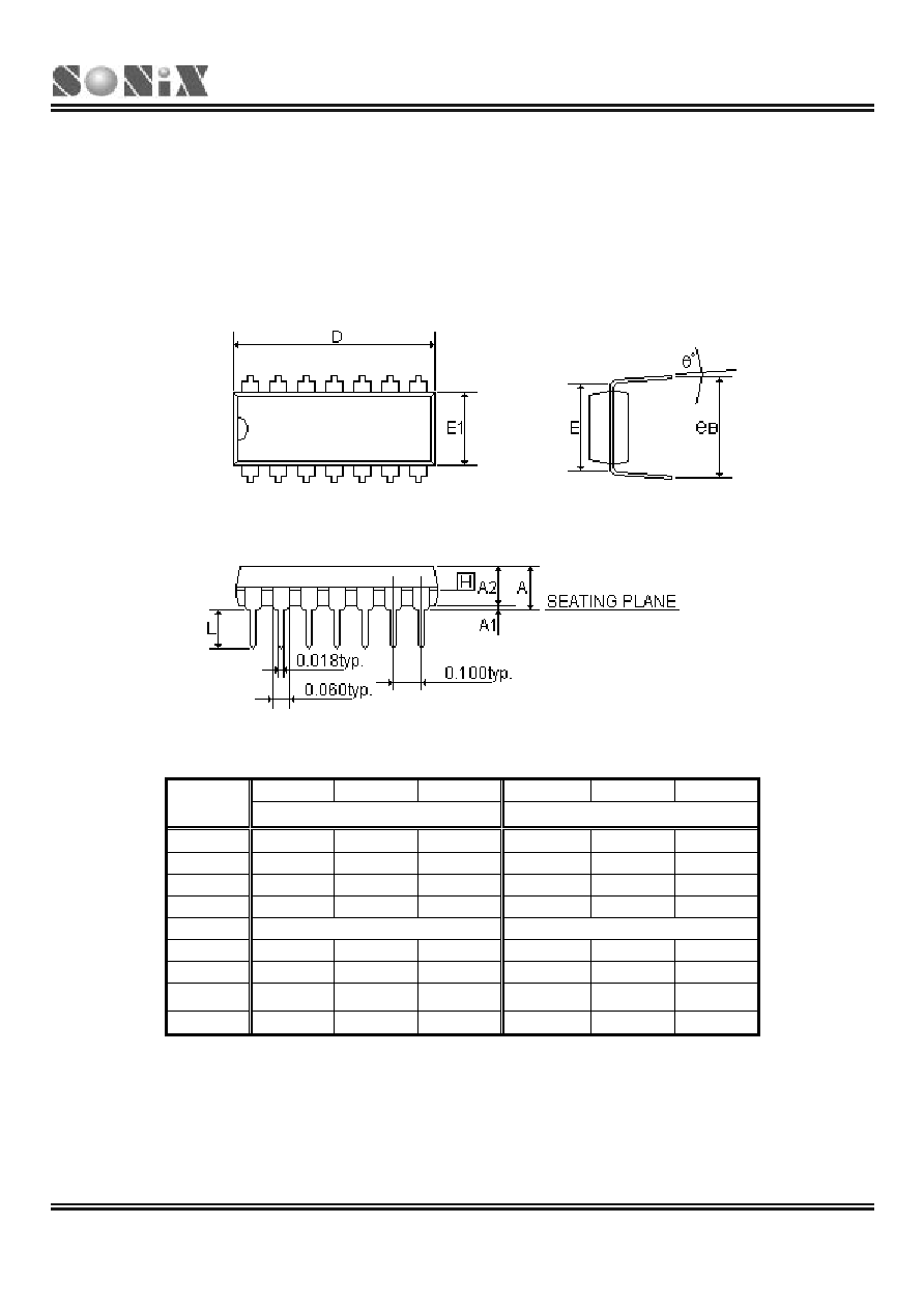
SN8P2501A
8-Bit Micro-Controller
SONiX TECHNOLOGY CO., LTD
Page 65
Preliminary Version 0.2
1
1
1
1
1
1
PACKAGE INFORMATION
11.1 P-DIP 14 PIN
MIN NOR MAX MIN NOR MAX
SYMBOLS
(inch) (mm)
A - -
0.210
- -
5.334
A1 0.015 -
- 0.381 -
-
A2 0.125
0.130
0.135 3.175 3.302
3.429
D 0.735
0.075
0.775
18.669
1.905
19.685
E 0.300
7.62
E1 0.245
0.250
0.255 6.223 6.35 6.477
L 0.115
0.130
0.150
2.921
3.302
3.810
B
0.335 0.355 0.375 8.509 9.017 9.525
∞ 0∞ 7∞ 15∞ 0∞ 7∞ 15∞
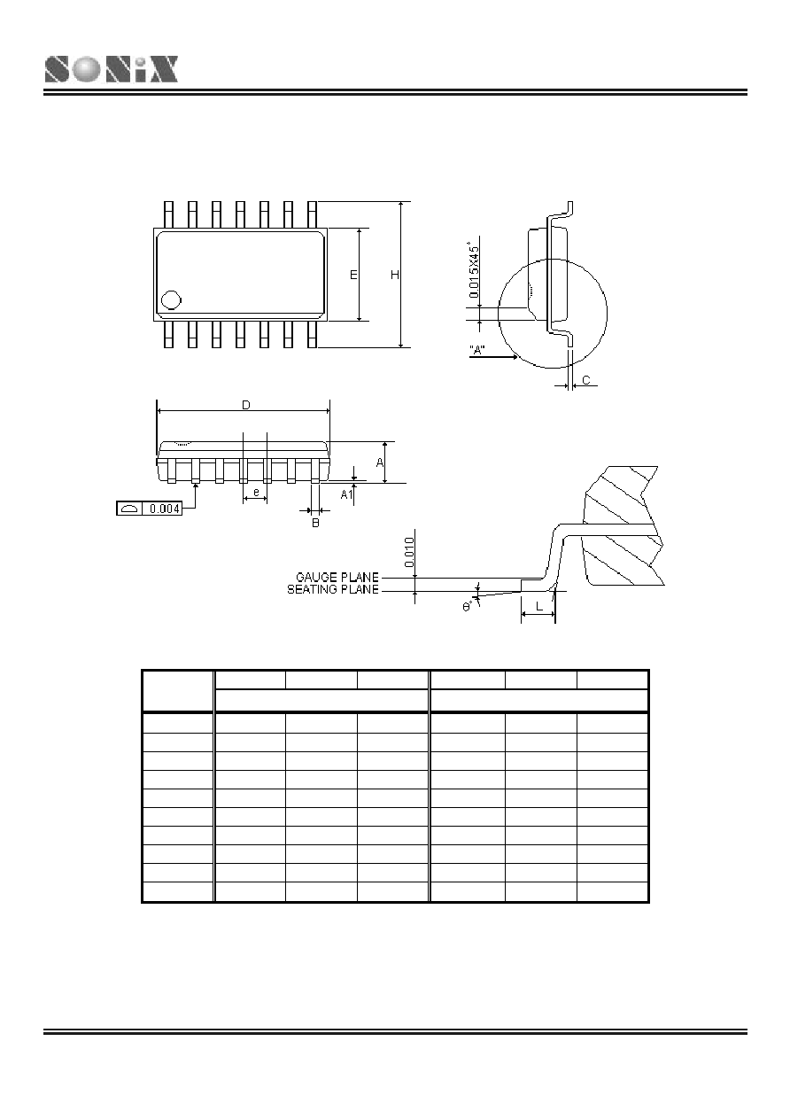
SN8P2501A
8-Bit Micro-Controller
SONiX TECHNOLOGY CO., LTD
Page 66
Preliminary Version 0.2
11.2 SOP 14 PIN
MIN NOR MAX MIN NOR MAX
SYMBOLS
(inch) (mm)
A 0.058
0.064
0.068
1.4732
1.6256
1.7272
A1 0.004 - 0.010
0.1016 - 0.254
B 0.013
0.016
0.020
0.3302
0.4064
0.508
C 0.0075 0.008 0.0098 0.1905 0.2032 0.2490
D 0.336
0.341
0.344
8.5344
8.6614
8.7376
E 0.150
0.154
0.157 3.81
3.9116
3.9878
e -
0.050
- -
1.27
-
H 0.228
0.236
0.244
5.7912
5.9944
6.1976
L 0.015
0.025
0.050
0.381
0.635
1.27
∞ 0∞ - 8∞ 0∞ - 8∞
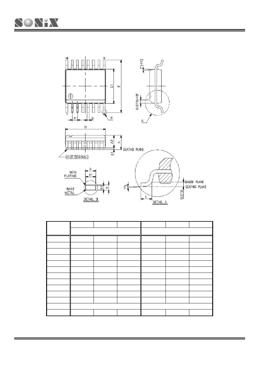
SN8P2501A
8-Bit Micro-Controller
SONiX TECHNOLOGY CO., LTD
Page 67
Preliminary Version 0.2
11.3 SSOP 16 PIN
MIN NOR MAX MIN NOR MAX
SYMBOLS
(inch) (mm)
A 0.053 - 0.069
1.3462
-
1.7526
A1 0.004 - 0.010
0.1016
-
0.254
A2 - -
0.059 -
-
1.4986
b 0.008 - 0.012
0.2032
-
0.3048
b1 0.008 - 0.011
0.2032
-
0.2794
c 0.007 - 0.010
0.1778
-
0.254
c1 0.007 - 0.009
0.1778
-
0.2286
D 0.189 - 0.197
4.8006
-
5.0038
E1 0.150 - 0.157 3.81
-
3.9878
E 0.228 - 0.244
5.7912
-
6.1976
L 0.016 - 0.050
0.4064
-
1.27
e
0.025 BASIC
0.635 BASIC
∞ 0∞ - 8∞ 0∞ - 8∞

SN8P2501A
8-Bit Micro-Controller
SONiX TECHNOLOGY CO., LTD
Page 68
Preliminary Version 0.2
SONIX reserves the right to make change without further notice to any products herein to improve reliability, function or
design. SONIX does not assume any liability arising out of the application or use of any product or circuit described herein;
neither does it convey any license under its patent rights nor the rights of others. SONIX products are not designed,
intended, or authorized for us as components in systems intended, for surgical implant into the body, or other applications
intended to support or sustain life, or for any other application in which the failure of the SONIX product could create a
situation where personal injury or death may occur. Should Buyer purchase or use SONIX products for any such
unintended or unauthorized application. Buyer shall indemnify and hold SONIX and its officers , employees, subsidiaries,
affiliates and distributors harmless against all claims, cost, damages, and expenses, and reasonable attorney fees arising
out of, directly or indirectly, any claim of personal injury or death associated with such unintended or unauthorized use
even if such claim alleges that SONIX was negligent regarding the design or manufacture of the part.
Main Office:
Address: 9F, NO. 8, Hsien Cheng 5th St, Chupei City, Hsinchu, Taiwan R.O.C.
Tel: 886-3-551 0520
Fax: 886-3-551 0523
Taipei Office:
Address: 15F-2, NO. 171, Song Ted Road, Taipei, Taiwan R.O.C.
Tel: 886-2-2759 1980
Fax: 886-2-2759 8180
Hong Kong Office:
Address: Flat 3 9/F Energy Plaza 92 Granville Road, Tsimshatsui East Kowloon.
Tel: 852-2723 8086
Fax: 852-2723 9179
Technical Support by Email:
Sn8fae@sonix.com.tw