
SNL310
16-Bit LCD Controller
======== CONTENTS ========
1.
INTRODUCTION............................................................................................................... 3
2.
FEATURES ....................................................................................................................... 3
3.
PIN ASSIGNMENTS ......................................................................................................... 4
4.
I/O PORT........................................................................................................................... 5
5.
TIMER/COUNTER ............................................................................................................ 6
6.
Real Time Clock (RTC).................................................................................................... 6
7.
DA & PWM ........................................................................................................................ 6
7.1
DAC............................................................................................................................... 6
7.2
PWM.............................................................................................................................. 7
8.
EXTENSION BUS ............................................................................................................. 8
8.1
Extension Bus for External Memory Device ................................................................. 8
9.
UART INTERFACE......................................................................................................... 13
10.
LCD DRIVER INTERFACE ........................................................................................ 13
10.1
8-Bit Interface.............................................................................................................. 13
10.2
1-Bit Interface.............................................................................................................. 16
10.3
LCD RAM Assignment ................................................................................................ 16
10.4
LCD RAM Mapping ..................................................................................................... 17
10.5
LCD Interface Configuration ....................................................................................... 18
11.
APPLICATION DIAGRAM ......................................................................................... 20
11.1
Application 1................................................................................................................ 20
11.2
Application 2................................................................................................................ 21
12.
BONDING PAD........................................................................................................... 22
13.
ABSOLUTE MAXIMUM RATINGS ............................................................................ 23
14.
ELECTRICAL CHARACTERISTICS.......................................................................... 23
Ver: 1.7
May 2, 2003
1
SNL310
16-Bit LCD Controller
AMENDENT HISTORY
Version Date
Description
Ver 1.5 October 28, 2002
V1.5 first issue
Ver 1.6 March 27, 2003
Add revision history
Update application circuit
Page4: AP3.0~P3.10 -> P3.0~P3.10
Page10: Update addressing capability of Table-2,
Figure-7 & Figure-8
Page12, 13: modify the read/write wave-form of external
memory
Page25: Add one resister between CVDD and VDD for 3
batteries application.
Ver 1.7 May 2, 2003
Final released version
Ver: 1.7
May 2, 2003
2

SNL310
16-Bit LCD Controller
1. INTRODUCTION
SNL310 is a high performance 16-bit DSP base processor with an 8-bit
microprocessor interface to
drive various external devices, such as standard mask
ROM, Flash, SRAM and 1-bit/8-bit interface LCD drivers. Besides, this chip also
provides a UART interface to communicate with PC or other devices This chip is
not
only a simply controller but also a powerful software voice synthesizer to realize voice
hi-compression, 4-ch wave-table melody.
2. FEATURES
-
-
-
Power supply: 2.4V ~ 3.6V (for 2 batteries application)
3.6V ~ 5.1V (for 3 batteries application)
Built-in 16-bit DSP
Software-based voice/melody processing
Rich Function Instruction Set
16MHz crystal or R-C type oscillator for system clock
8 MIPS CPU performances under 16MHz
I/O Ports: 64 I/O pins (P2.0~P2.15, P3.0~P3.15, P4.0~P4.15 and P5.0~P5.15)
ROM size: 96K*16 bits
RAM size: 4k*16 bits (including LCD RAM)
8 Interrupt Sources
4 internal interrupt (T0, T1, T2 and RTC)
3 external interrupt (P3.0~P3.2)
1 DA/PWM output
Two voice/melody channels or 4 channels wave-table melody
Three 8-bit timers with auto-reload function
Built-in 32768 crystal for Real Time Clock
Built in PWM direct drive circuit and fixed current D/A output
Sampling Rate: 4KHz ~16KHz
Built-in software voice synthesizer for multiple bit-rate solution
UART interface provided
Ver: 1.7
May 2, 2003
3
SNL310
16-Bit LCD Controller
3. PIN ASSIGNMENTS
Symbol
Descriptions
No. of PIn Pin Count
XIN
High speed clock crystal input / RC-type oscillator input
1
1
XOUT
High speed clock crystal output / RC-type oscillator input
1
2
LXIN
Low speed clock crystal input
1
3
LXOUT
Low speed clock crystal output
1
4
CKSEL
Crystal/RC-type oscillator select for high speed clock
1
5
BP0
PWM output 1
1
6
BN0
PWM output 2
1
7
VO DA
output
1
8
RST Chip
reset
1
9
CVDD
Positive power supply for core circuit
2
11
VDD
Positive power supply
6
17
GND
Negative power supply
8
25
TEST
For test only
1
26
P2.0~P2.15 General I/O port P2.0~P2.15
16
42
P3.0~P3.10 General I/O port P3.0~P3.10
P3.0: INT0 / RxD pin of UART interface
P3.1: INT1 / TxD pin of UART interface
P3.2: INT2
P3.3: IR output
P3.4~P3.5: general I/O
P3.6: LCD serial data output (LSD)
P3.7: LCD serial mode clock out1 (LCO1)
P3.8: LCD serial mode clock out2 (LCO2)
P3.9: LCD frame inversion control
P3.10: COM data synchronize signal / E_R
P3.11~P3.14: chip select pin CS3~CS0
P3.15:address pin A[22] for 16-bit mode of extension
Bus
16 58
P4.0~P4.15 General I/O port P4.0~P4.15
Address bus A[0..15] of external device interface
16 74
P5.0~P5.15 General I/O port
P5.0~P5.5: address bus A[16..21] of external device interface
P5.6: WRB / RDB of external device interface
P5.7: Enb / RDB of external device interface
P5.8~P5.15: data bus D[0..7] of extension bus
16 90
Ver: 1.7
May 2, 2003
4
SNL310
16-Bit LCD Controller
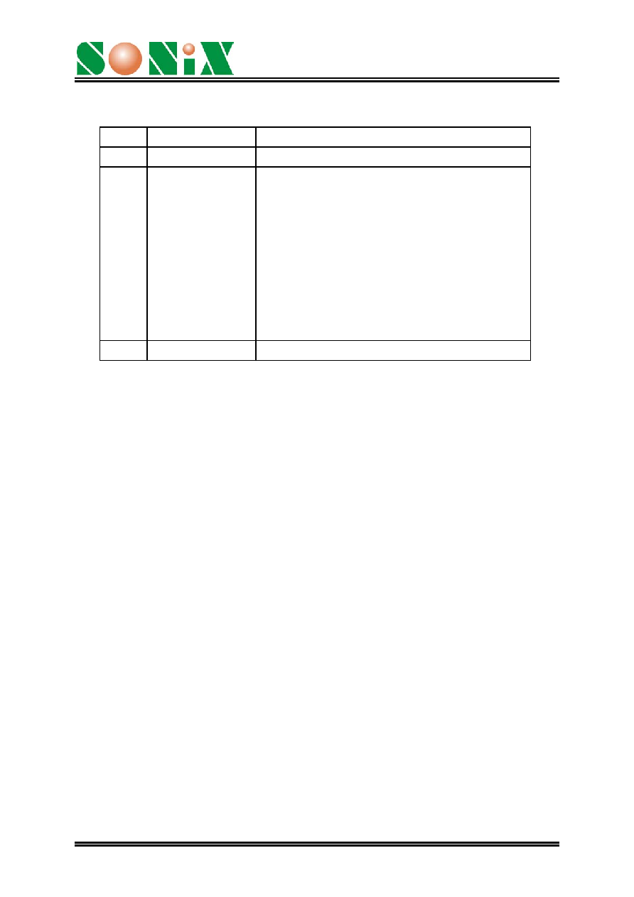
4. I/O PORT
SNL310 provides totally 64 I/O pins (P2.0~P2.15, P3.0~P3.15, P4.0~P4.15, and
P5.0~P5.15). The input pull high resistor of each pin can be programmed by Port
Pull-High Register and the direction of I/O port is selected by Port Direction Register.
The Port2 (P2.0~P2.15) and Port3 (P3.0~P3.15) can wake the chip up from the stop
mode and watch mode.
These 64 programmable I/O pins provides not only a simply input/output function but
also flexible configuration. It can be configured to be an 8-bit microprocessor interface
to drive external devices, such as mask ROM, Flash and SRAM and LCD driver.
Furthermore, the pins "TxD" and "RxD" are shared with P3.0 and P3.1.
The internal structure of I/O pins is showed in Figure-2.
Pull-Up
Resister
Latch
PAD
to internal bus
Pull-Up
Select
In/Out
Control
In/Out
Control
I/O Configuration of Port2 ~ Port5
Figure-2
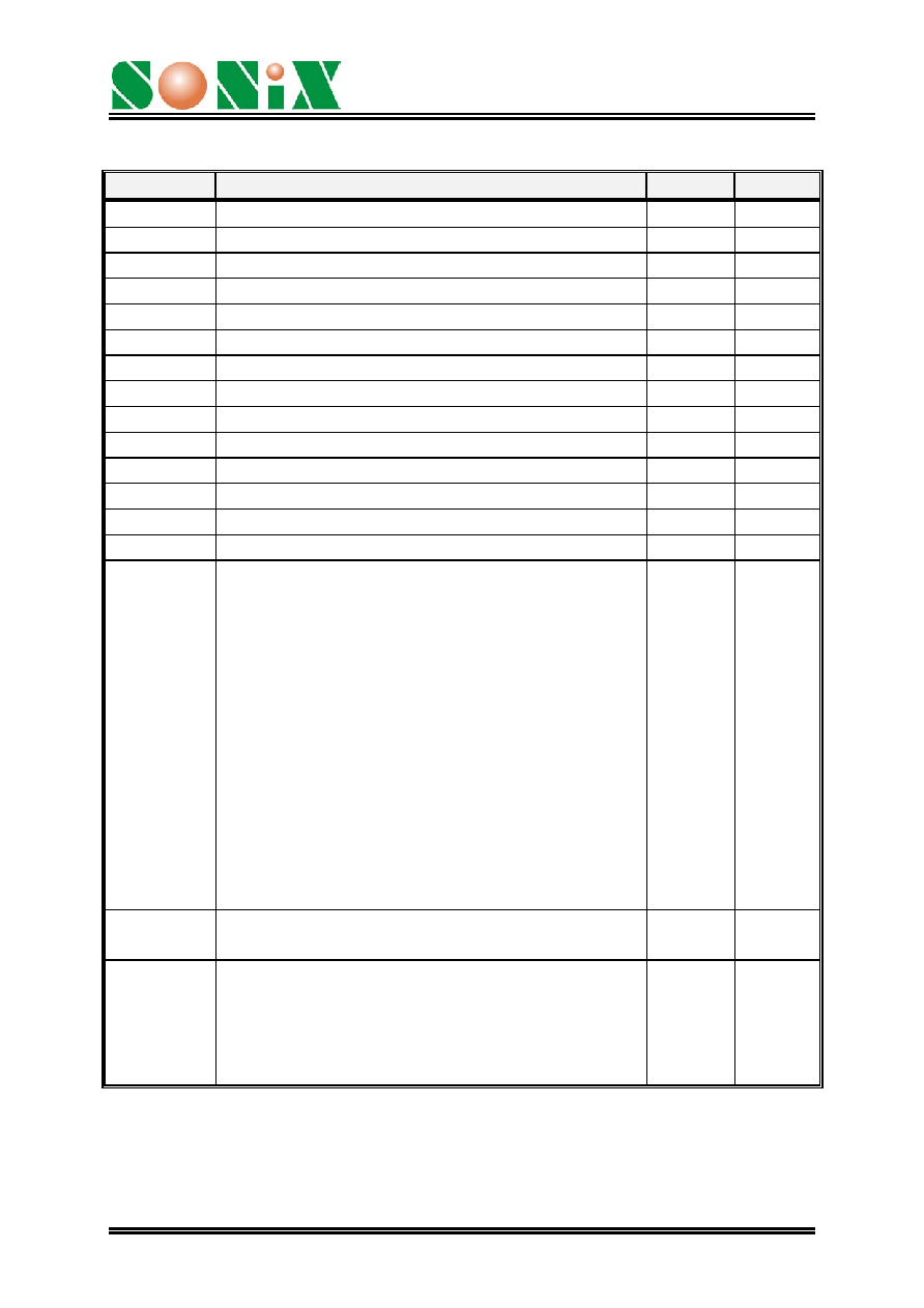
In some applications (e.g., Infra Red, IR), an output port needs to be modulated a carry
signal. In the cases, the routine of modulation will occupy too many CPU computations.
Thus, a modulation circuit is built in chip to reduce CPU's loading,
Timer2
overflow
P3.3
2
IREN
I/O Pad
Figure-3
Ver: 1.7
May 2, 2003
5
SNL310
16-Bit LCD Controller
The modulation function will be active when the control bit "IREN" set to "1". And
setting timer2 can generate the frequency of carry signal.
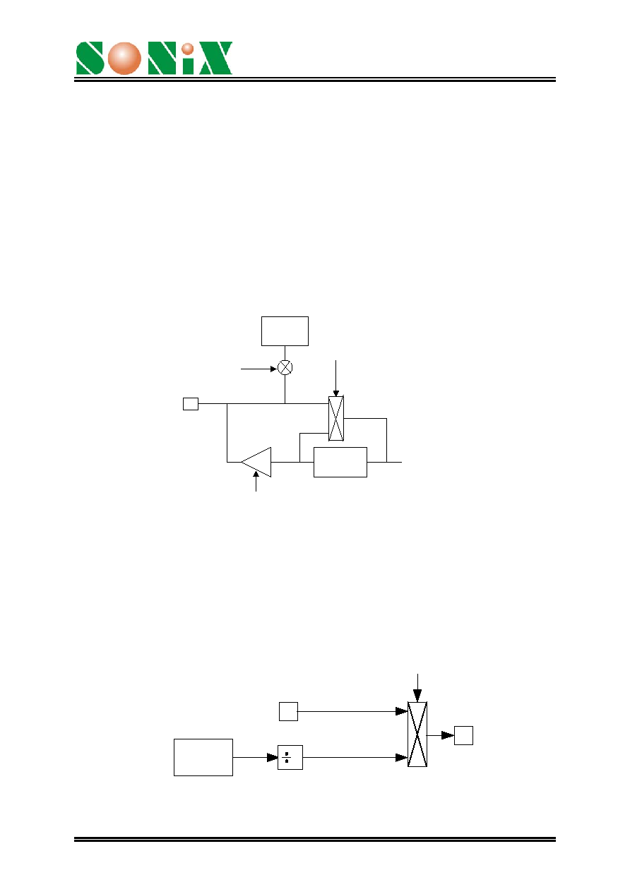
5. TIMER/COUNTER
SNL310 provides three 8-bit timer/event counters (T0/T1/T2). Each timer is 8-bit
binary up-count timer with pre-scalar and auto-reload function. Timer 0 (T0) was
used when voice playing, so user should avoid to use T0.
(system clock)/2*
Auto-reload
clear
comparator
MUX
/256
/8
/4
/2
If equal, Time out
8-bit Up
Counter
Enable
Pre-scalar
TnC (8-bit)
Figure-4
6. Real Time Clock (RTC)
To realize the watch function, 0.25s RTC (real time clock) is built in the chip. The real
time clock has two clock sources. One is from system clock (16MHZ) and another one
is from low-speed clock source (32768HZ). Once the RTC function is enabled, the
RTC circuit will generate an interrupt request per 0.25 second.
If chip is in power-down mode and interrupt enable is active for RTC, then chip will be
wake-up from power-down mode per 0.25 second.
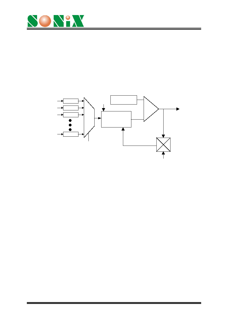
7. DA & PWM
To play out voices, SNL310 contains two different solutions for the user's
applications, DAC and PWM. The user can choose one of these two solutions in this
design. Only one function can be activated at one time.
7.1 DAC
A 10-bit current type digital-to-analog converter is built-in SNL310. The relationship
between input digital data and output analog current signal is listed in the following
table. Also, the recommended application circuit is illustrated as follows.
Ver: 1.7
May 2, 2003
6

SNL310
16-Bit LCD Controller
Input data
Typical value of output current (mA)
0 0
1 3/1024
...
n n*(3/1024)
...
1024 3
7.2 PWM
A PWM (pulse width modulation) circuit is built-in SNL310. PWM can convert input
digital data into pulse trains with suitable different pulse width. The maximum
resolution of PWM is 10 bits. Two huge output stage circuits are included in SNL310.
Both of them are capable of driving speaker directly. The recommended application
circuit is as follows.
VCC
BUO1/VO
1K
BUO1/VO
BUO2
DAC output
PWM output
Ver: 1.7
May 2, 2003
7

SNL310
16-Bit LCD Controller
8. EXTENSION BUS
SNL310 totally provides 64 I/O pins, those I/O pins can be configured to be address,
data and control signal of extension bus except P2.0~P2.15 are the dedicated general
I/O pins. Table-1 shows the relation among P3.5~P3.15, P4.0~P4.15, P5.0~P5.7 and
I/O pins.
I/O Pin
Extension Bus
Descriptions
P3.10
E_R
RD signal for 6800 interface
P3.15
A[22]
Address pin of 16-bit mode memory accessing
P3.11~P3.14 CS3~CS0
Chip select pin
P4.0~P4.15
A[0..15]
Address bus
P5.0~P5.5 A[16..21]
Address
bus
P5.6 WR/RD
Write
signal
P5.7 RD/E
Read
signal
P5.8~P5.15 D[0..7]
Data
bus
Table-1
SNL310 provides four chip select pins for external devices, each chip select pin can be
connected to memory device or LCD driver. Besides, all the address, data and control
pins of extension bus are shared with general I/O pins. Normally, the default setting is
general I/O pins for extension bus. User just need to set the enable control bit of
extension bus then all the corresponding I/O pins will switch to be extension bus
automatically.
8.1 Extension Bus for External Memory Device
SNL310 provides two access modes for external memory device. One
is 8-bit mode
and another one is 16-bit mode. User has to use 16-bit mode if executed user's
program is from external memory. Most important of all, SNL310 only can execute
user's program from the first external device. So user has to connect Mask ROM or
Flash which already burn-in user's program to the "CS1"
A0
A21
A21
SNL310
A0
CE\
CS1
mask ROM/
Flash
A22
A0
A22
A22
SNL310
A0
CE\
CS1
mask ROM/
Flash
8-bit Mode of Extension Bus
16-bit Mode of Extension Bus
Figure-5
Ver: 1.7
May 2, 2003
8
SNL310
16-Bit LCD Controller
:
:
:
:
0x000000
0x000001
0x000002
Byte1
0x000003
0x000004
0x000005
:
:
:
:
Byte2
Byte3
Byte4
Byte5
Byte6
Word 1
Word 2
ROM/Flash/SRAM
Read from
SNL310
:
:
:
:
0x000000
0x000001
0x000002
Byte1
0x000003
0x000004
0x000005
:
:
:
:
Byte2
Byte3
Byte4
Byte5
Byte6
Byte1
ROM/Flash/SRAM
Byte2
Read from
SNL310
Figure-6
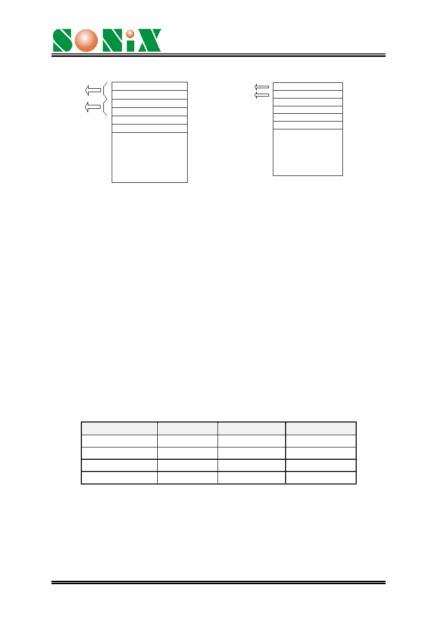
Figure-5 shows the hardware connection for 8-bit/16-bit mode for external memory
accessing. The memory size calculation of each external memory device is a little
difference between 8-bit and 16-bit mode because of
the address pin "A[22]".
In 16-bit mode, "A[22]" pin can be connected to external memory. And chip will read
one byte data from external memory twice to get a complete 16-bit instruction code or
data. So the maximum memory size can support up to 64M bits of each device.
In 8-bit mode, considering the memory mapping issue, user can't connected "A[22]"
pin to external memory. So the maximum memory size can support up to 32M bits.
Figure-6 figures out how the data be read from external memory in 8-bit/16-bit mode.
However, all the data access from external memory is treated as RAM accessing
except executes user's program from external memory. User should use indirection
RAM access instruction to read data from external memory. Therefore, each chip
selects pin representing a RAM bank in memory allocation of SNL310.
Device No.
RAM bank
Start address
End Address
1
st
external device 0x008 ~ 0x03F
0x0080000
0x03FFFFF
2
nd
external device 0x040 ~ 0x07F
0x0400000
0x07FFFFF
3
rd
external device 0x080 ~ 0x0BF
0x0800000
0x0BFFFFF
4
th
external device 0x0C0 ~ 0x0FF
0x0C00000
0x0FFFFFF
Table-2 Addressing Capability (16-Bit Mode)
Ver: 1.7
May 2, 2003
9

SNL310
16-Bit LCD Controller
The addressing capacity of each external device is showed in Table-2. The memory
allocation of each bank is 64K words and the addressing region of each device totally
includes
64 banks except 1
st
device. In fact, the RAM bank of 1
st
device is shared with
internal memory of SNL310, so there are only 56 banks in the first device. In another
hand, user can not use full memory location in the first device. The actual addressing
capacity of first device is less than 64M bits (64M bits � 8M bits) = 56M bits in 16-bit
mode.
User's Data
or
Program
32M Bit Non-Use
32M Bits
0x0000000
0x03FFFFF
0x01FFFFF
64M Bits
0x0200000
Figure-7
User's Data
or
Program
8M Bit Non-Use
56M Bits
0x0000000
0x03FFFFF
0x0040000
0x003FFFF
64M Bits
Figure-8
Ver: 1.7
May 2, 2003
10
SNL310
16-Bit LCD Controller
In Figure-7, CS0 of SNL310 connected a 32M-bit memory. So the useful addressing capacity
is from 0x0200000 ~ 0x3FFFFF.
In Figure-8, CS0 of SNL310 connected a 64M-byte memory. So the useful addressing
capacity is from 0x0040000 ~ 0x03FFFFF.
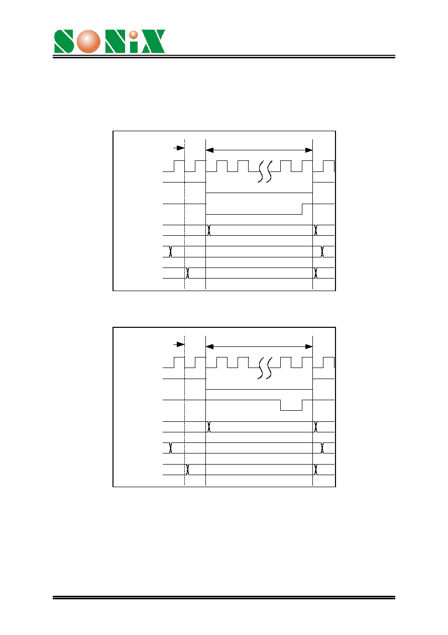
(Complete Read Cycle)
CLOCK
CS\
RD\
A[0..22]
IN D[0..7]
OUT D[0..7]
62.5ns
2 * n * clocks
(Complete Write Cycle)
CLOCK
CS\
WR\
A[0..22]
IN D[0..7]
OUT D[0..7]
62.5ns
2 * n * clocks
Access timing for 8-bit mode
Figure-9
Ver: 1.7
May 2, 2003
11
SNL310
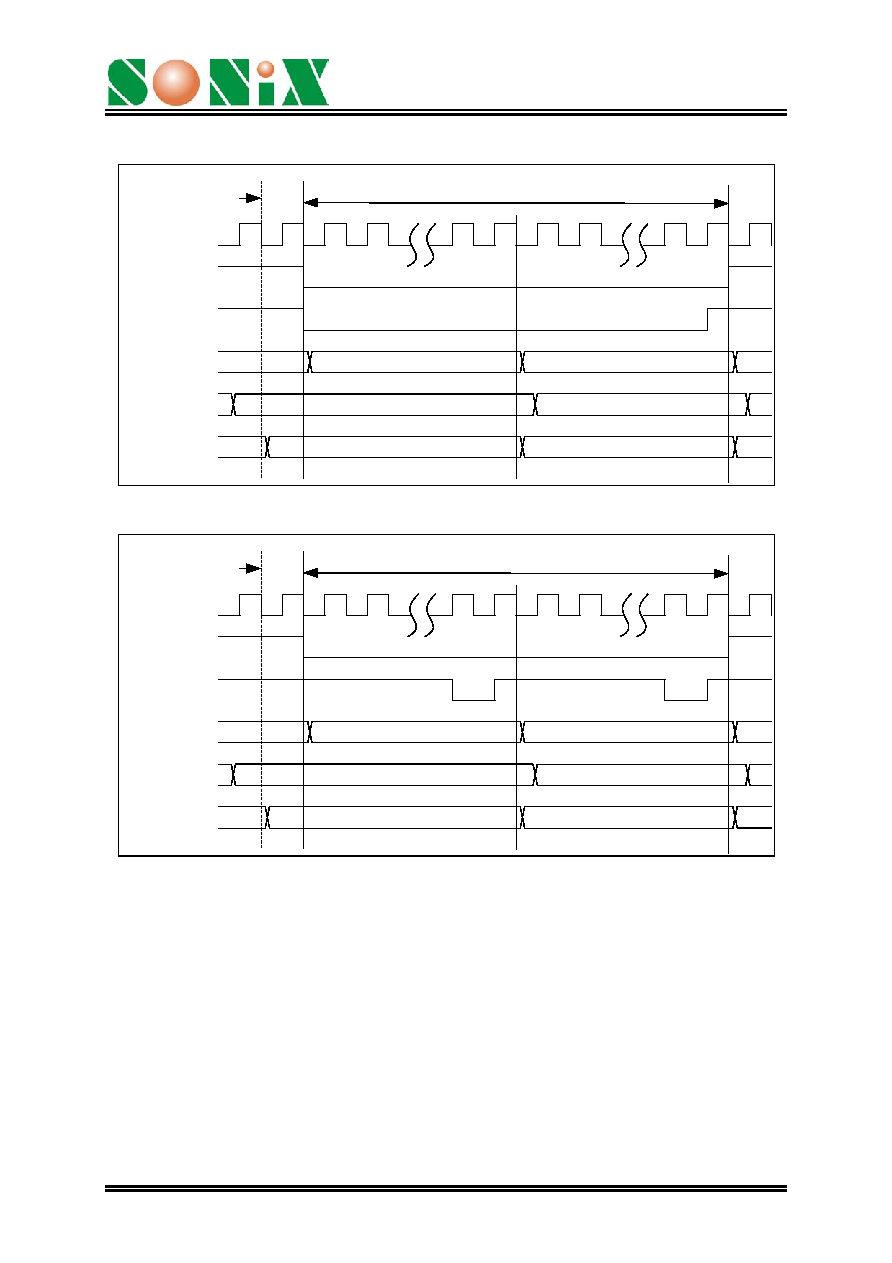
16-Bit LCD Controller
CLOCK
CS\
RD\
A[0..22]
IN D[0..7]
OUT D[0..7]
62.5ns
(Complete Read Cycle)
4 * n * clocks
CLOCK
CS\
WR\
A[0..22]
IN D[0..7]
OUT D[0..7]
62.5ns
(Complete Write Cycle)
4 * n * clocks
Access timing for 16-bit mode
Figure-10
Figure-9 and Figure-10 show the accessing timing for 8-bit mode and 16-bit mode.
Considering to compatible with different access time memory, user can set different
speed ratio in the special register "EDI" (External Device Information register). The
value "n" in Figure-9 and Figure-10 is relative to the setting of speed ratio of EDI
register.
Ver: 1.7
May 2, 2003
12

SNL310
16-Bit LCD Controller
9. UART INTERFACE
The built-in UART supports the serial data transmission. SNL310 provides data
phase auto-clock calibration function. The RxD pin and TxD pin are shared with P3.0
& P3.1, and user can switch P3.0 and P3.1 to be RxD and TxD by configuring the
RxD/TxD enable bit of UARTC register. User can configure the baud rate of UART
from 1200bps to 115200bps just by using the single crystal system (16MHZ crystal).
All the clock base of baud rate is counting by Timer2.
10. LCD DRIVER INTERFACE
10.1 8-Bit Interface
The extension bus of SNL310 supports not only external memory device but also 8-bit
8080/6800 microprocessor interface for external LCD controller which already built-in
LCD display RAM. User should enable extension bus before driving external LCD
driver, and define the chip select pin you used to connect to LCD driver in EBC
register.
In 8-bit interface LCD controller, LCD display data is stored in LCD driver. Any change
of LCD display is sent out to external LCD driver's RAM by addressing different SRAM
space. The interface emulates the 8080/6800-series interface to speed up the
interface data moving processing.
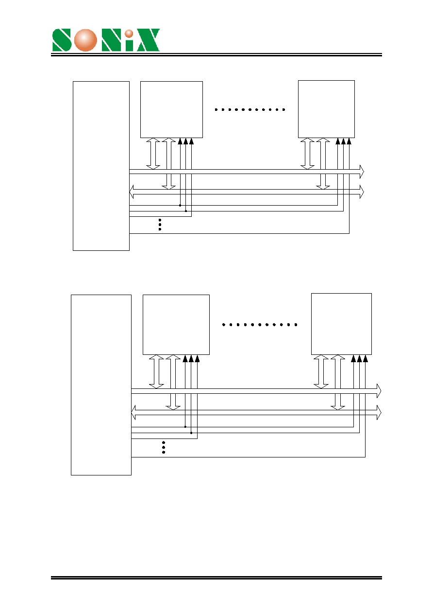
Figure-11 and Figure-12 are the timing diagrams between SNL310 and LCD driver by using
8-bit 8080/6800 interface.
Ver: 1.7
May 2, 2003
13
SNL310
16-Bit LCD Controller
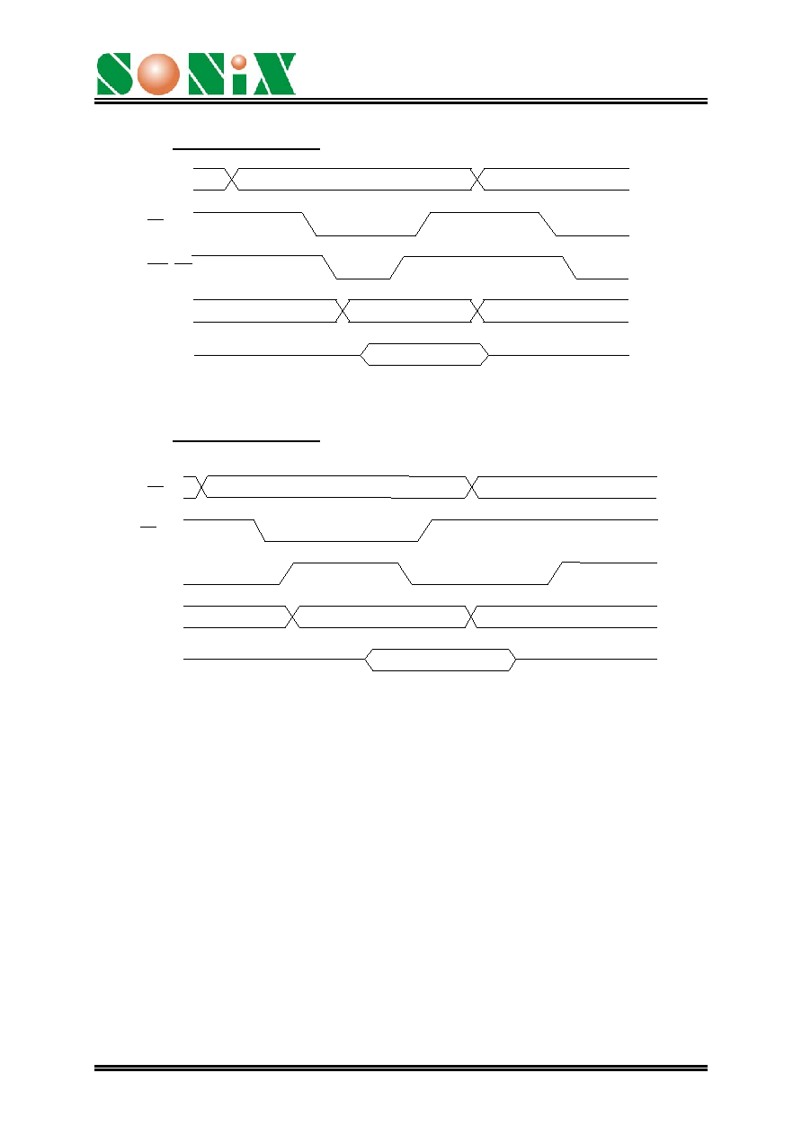
8080-series Interface:
Figure-11
6800-series Interface:
A0
D0~D7
(WRITE)
D0~D7
(READ)
WR, RD
CS
E
D0~D7
(WRITE)
D0~D7
(READ)
A0
R/W
CS
Figure-12
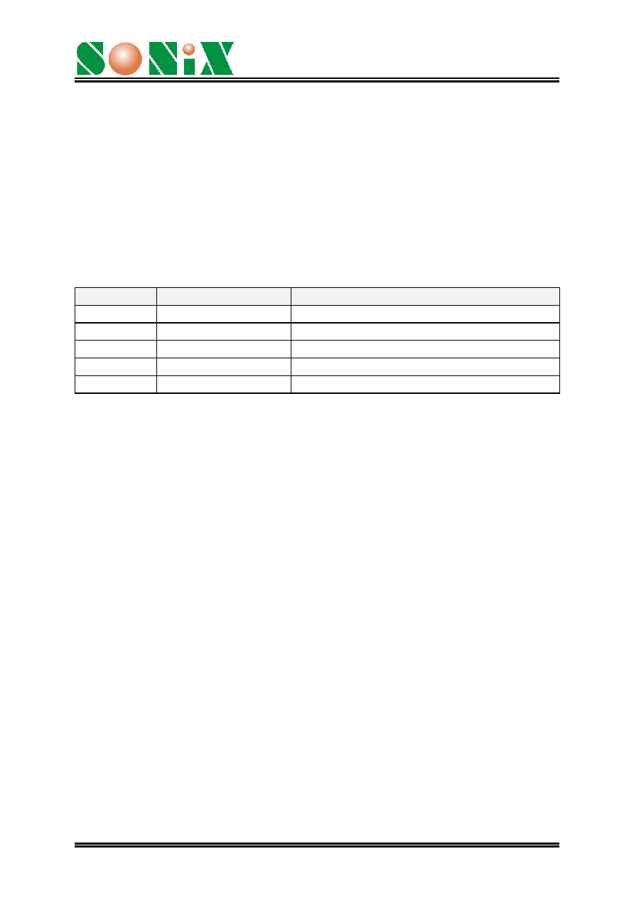
In SNL310, the interface with external 8-bit mode LCD driver is shared with extension
bus. When LCD driver connected to SNL310, chip will allocate a memory area for LCD
driver and the size of this memory area will depend on unit size of each external device.
So it is easy to configure LCD driver and read/write data to/from LCD driver. Figure-13
and Figure-14 show out the system connection of 808/6800 LCD interfaces between
SNL310 and LCD driver.
Ver: 1.7
May 2, 2003
14
SNL310
16-Bit LCD Controller
A[0..21]
D[0..7]
RD
A[0..21]
D[0..7]
CS0
CS1
address bus
data bus
Memory
CS2
CS3
A0
D[0..7]
LCD Driver
SNL310
WR CE
WR
RD
RD WR CS1
8080 LCD driver interface
Figure-13
A[0..21]
D[0..7]
RD
A[0..21]
D[0..7]
CS0
CS1
address bus
data bus
Memory
CS2
CS3
A0
D[0..7]
LCD Driver
SNL310
WR CE
WR
E_RD
E WR CS1
6800 LCD driver interface
Figure-14
Ver: 1.7
May 2, 2003
15
SNL310
16-Bit LCD Controller
10.2 1-Bit Interface
SNL310 supports not just 8-bit interface but also 1-bit interface LCD driver. For this
kind LCD driver doesn't include display RAM. All the display data is stored in host CPU.
So host CPU has to specify a dedicate interface to drive LCD driver. Beside the
interface, SNL310 reserves
the last 2K words RAM (0x0800~0x0FFF) for stored the
display data, then interface circuit will send accurate signal to LCD driver
automatically.
P3.6~P3.10 can be configured to be 1-bit interface for LCD driver just by property
setting control register. Table-3 shows the relation between P3.6~P3.10 and LCD
driver interface.
I/O Pin
Extension Bus
Descriptions
P3.6
LSD
LCD serial data output
P3.7
LCO1
LCD serial mode clock out1
P3.8
LCO2
LCD serial mode clock out2
P3.9
LFC
LCD frame inversion control
P3.10
COMS
COM data synchronize signal
Table-3
10.3 LCD RAM Assignment
Generally, those 1-bit interface LCD drivers don't built-in the LCD display RAM. All the
display data have been stored in CPU side. The SNL310 already built-in totally 4K
words RAM, so user can set a property value of LCD RAM start address (LRSA)
register to assign a RAM location for LCD display data. The start address setting
formula is shown as bellow:
Calculating formula of start address
If SEG number divided by 16
4096-(SEG numbe/16)*COM number => for B/W
4096-(SEG numbe/16)*COM number*2 => for 4 gray levels
If SEG number can't divided by 16
4096-((SEG numbe/16)+1)*COM number => for B/W
4096-((SEG numbe/16)+1)*COM number*2 => for 4 gray levels
Once upon user set the start address of LCD display RAM and active this interface
function, chip will send the display data out to external LCD driver at the right time.
Ver: 1.7
May 2, 2003
16
SNL310
16-Bit LCD Controller
10.4 LCD RAM Mapping
65COM X 128SEG
SEG 0...............15 16..............31 ..................... 104...........119 120...........127
Bit0.............Bit15 Bit0.............Bit15
.....................
Bit0.............Bit15 Bit0.............Bit15
COM0
0x0DF8 0x0DF9
.....................
0x0DFE 0x0DFF
COM1
0x0E00 0x0E01
.....................
0x0E06 0x0E07
:
: : : : :
:
: : : : :
:
: : : : :
COM63
0x0FF0 0x0FF1
.....................
0x0FF6 0x0FF7
COM64
0x0FF8 0x0FF9
.....................
0x0FFE 0x0FFF
64COM X 128SEG
SEG 0...............15 16..............31 ..................... 104...........119 120...........127
Bit0.............Bit15 Bit0.............Bit15
.....................
Bit0.............Bit15 Bit0.............Bit15
COM0
0x0E00 0x0E01
.....................
0x0E06 0x0E07
COM1
0x0E08 0x0E09
.....................
0x0E0E 0x0E0F
:
: : : : :
:
: : : : :
:
: : : : :
COM62
0x0FF0 0x0FF1
.....................
0x0FF6 0x0FF7
COM63
0x0FF8 0x0FF9
.....................
0x0FFE 0x0FFF
48COM X 128SEG
SEG 0...............15 16..............31 ..................... 104...........119 120...........127
Bit0.............Bit15 Bit0.............Bit15
.....................
Bit0.............Bit15 Bit0.............Bit15
COM0
0x0E80 0x0E81
.....................
0x0E8E 0x0E8F
C0M1
0x0E90 0x0E91
.....................
0x0E96 0x0E97
:
: : : : :
:
: : : : :
:
: : : : :
COM46
0x0FF0 0x0FF1
.....................
0x0FF6 0x0FF7
COM47
0x0FF8 0x0FF9
.....................
0x0FFE 0x0FFF
Ver: 1.7
May 2, 2003
17

SNL310
16-Bit LCD Controller
32COM X 128SEG
SEG 0...............15 16..............31 ..................... 104...........119 120...........127
Bit0.............Bit15 Bit0.............Bit15
.....................
Bit0.............Bit15 Bit0.............Bit15
COM0
0x0F00 0x0F01
.....................
0x0F06 0x0F07
C0M1
0x0F08 0x0F09
.....................
0x0F0E 0x0F0F
:
: : : : :
:
: : : : :
:
: : : : :
COM31
0x0FF0 0x0FF1
.....................
0x0FF6 0x0FF7
COM32
0x0FF8 0x0FF9
.....................
0x0FFE 0x0FFF
:
:
10.5 LCD Interface Configuration
There are thee control registers (LCDC, COMN and SEGN) to configure hardware to
generate correct interface signal for LCD driver. The COMN and SEGN register are
used to specify how many common and segment number of LCD display. And the
LCDC register is the most important configuration register for this interface. For the
detail setting is showed as bellow:
LCD Configuration Register (LCDC)
LCDC initial value=0xxx xxx0 0000 0001
Bit
15 14 13 12 11 10 9 8 7 6 5 4 3 2 1 0
LCDC LCDEnb - - - - - - GrayC
Pre-Scalar
FRate
LCDEnb:
1-bit LCD interface enable control
0: disable
1: enable
GaryC:
Gray level control:
00: Blank/white 01: 2-level
10: 4-level
Pre-Scalar:
Define LCO1 clock rate
0x000: 16MHZ/4 0x001: 16MHZ/8
0x010: 16MHZ/16 0x011: 16MHZ/32
0x100: 16MHZ/64 0x101: 16MHZ/128
0X110: 16MHZ/256 0x111: 16MHZ/512
FRate:
0x0001: 256HZ (1/256 sec) 0x0010: 128HZ (2/256 sec)
0x0011: 85.3HZ (3/256 sec) 0x0100: 64HZ (4/256 sec)
: :
0x1111: 17HZ (15/256 sec)
Ver: 1.7
May 2, 2003
18
SNL310
16-Bit LCD Controller
NOTE:
1. The real Frame Rate
- For B/W display = FRate value/2
- For 2 gray level = FRate value/4
- For 4 gray level = FRate value/6
2. Pre-Scalar calculation formula
Formula:
Divider value * 2
15
> SEG number * (COM number+1) * 2
(pre-scalar value+1)
Example:
LCD display = 80com X 160seg (B/W display)
Frame Rate = 64
2 * 2
15
>160*(80+1)*2
(pre-scalar value+1)
Pre-scalar < = 1 (0x001)
Ver: 1.7
May 2, 2003
19
SNL310
16-Bit LCD Controller
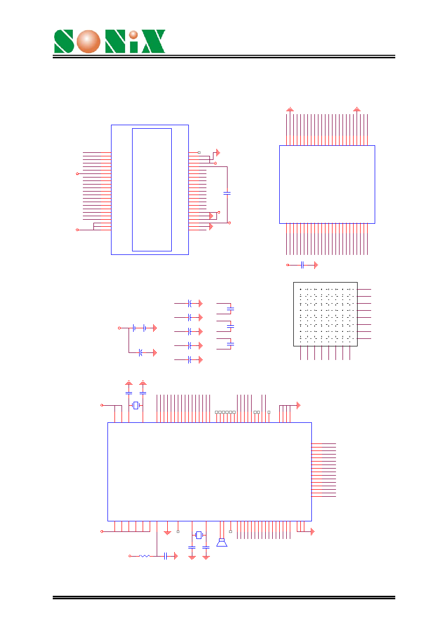
11. APPLICATION DIAGRAM
11.1 Application 1
3V/16M Crystal, with 8-Bit LCD driver and 32M Flash memory
C1
1uF
VDD
VDD
VDD
C9 1uF
C6 1uF
C4 1uF
C11
1uF
C8
1uF
C7
1uF
C5
1uF
C3
1uF
0
2
1
SPEAKER
4
3
6
5
(8 X 8 Matrix Key)
7
8
9
10
(3V Flash Memory)
11
12
VDD
14
13
1.5V
15
1.5V
VDD
Y1
32
76
8H
Z
C12
15p
F
C13
15p
F
VDD
2_1
1
2_9
2_8
2_1
4
2_1
2
2_1
0
2_1
5
2_1
3
C10
47uF
R1
220K
C16
0.1uF
VDD
Y2
16MHZ
C14
15pF
C15
15pF
U2
MX29LV320T/B
A15
1
A14
2
A13
3
A12
4
A11
5
A10
6
A9
7
A8
8
A19
9
A20
10
WE_
11
RESET_
12
A21
13
WP_/ACC
14
RY/BY_
15
A18
16
A17
17
A7
18
A6
19
A5
20
A4
21
A3
22
A2
23
A1
24
A0
25
CE_
26
GND
27
OE_
28
Q0
29
Q8
30
Q1
31
Q9
32
Q2
33
Q10
34
Q3
35
Q11
36
Vcc
37
Q4
38
Q12
39
Q5
40
Q13
41
Q6
42
Q14
43
Q7
44
Q15/A-1
45
GND
46
BYTE_
47
A16
48
U3
SNL310
VDD
3
VDD
19
VDD
37
VDD
48
CVDD
85
CVDD
26
GND
5
GND
17
GND
28
GND
41
GND
46
RST
83
BP0
47
BN0
49
VO
4
XIN
6
XOUT
7
LXIN
2
LXOUT
1
TESTM
53
CKSEL
52
P2.0
90
P2.1
89
P2.2
88
P2.3
87
P2.4
86
P2.5
82
P2.6
81
P2.7
80
P2.8
78
P2.9
77
P2.10
76
P2.11
75
P2.12
74
P2.13
73
P2.14
72
P2.15
71
GND
50
GND
84
P3.0
70
P3.1
69
P3.2
68
P3.3
67
P3.4
66
P3.5
65
P3.6
64
P3.7
63
P3.8
61
P3.9
59
P3.10
58
P3.11
57
P3.12
56
P3.13
55
P3.14
54
P3.15
51
P5.0
25
P5.1
24
P5.2
23
P5.3
22
P5.4
21
P5.5
20
P5.6
18
P5.7
16
P5.8
15
P5.9
14
P5.10
13
P5.11
12
P5.12
11
P5.13
10
P5.14
9
P5.15
8
P4.0
45
P4.1
44
P4.2
43
P4.3
42
P4.4
40
P4.5
39
P4.6
38
P4.7
36
P4.15
27
P4.14
29
P4.13
30
P4.12
31
P4.11
32
P4.10
33
P4.9
34
P4.8
35
VDD
60
VDD
79
132 X 65
U1
S6B1713
DUMMY
TEMPS
INTRS
HPM
DCDC5B
BSTS
V0
V1
V2
V3
V4
VR
C1-
C1+
C2-
C2+
C3-
C3+
VOUT
VDD
VSS
PS
MI
CLS
MS
DUTY1
DUTY0
DB7_SID
DB6_SCLK
DB5
DB3
DB2
DB1
DB0
E_RD
RW_WR
RS
RESETB
CS2
CS1B
DISP
CL
M
FRS
DUMMY
DB4
C2
0.1uF
VDD
VDD
VDD
CS0\
C1-
C1+
C2-
C2+
C3-
C3+
V0
V1
V2
V3
V4
D7
CE\
A
A
A
A
A
A
A
P2_0
A
P2_1
A
P2_2
A
A
P2_3
A
P2_4
A
A
P2_5
A
P2_6 P2_7
A
P2_8 P2_9 P2_10 P2_11 P2_12 P2_13
P2_15
P2_14
P2_2
P2_0
P2_1
P2_6
P2_4
P2_3
P2_7
P2_5
P
P
P
P
P
P
P
P
RST
A16
LSD LCO1 LCO2
COMD
FRAME
A18
A17
BYTE\
A19 A20
A0
D6
GND
A17
D5
D7
VDD
D2
D4
D3
D0
D1
GND
A1
OE\
CE\
A21
A13
A15
A10 A9
A14
A11
A12
A16
WR\RD
A21
A20
BUSY\
VDD A22 VDD
A19
A7 A6
A2
A18 A8
A5
A3
A4
RD
WR
D2
D1
D0
D3 D4
D6
D5
D7
D6
D5
D4
D3
D2
D1
D0
RD
C3+
C3-
C2+
C1-
C1+
C2-
V3
V4
V2
V1
V0
A1
WR
RST
CS0\
Ver: 1.7
May 2, 2003
20
SNL310
16-Bit LCD Controller
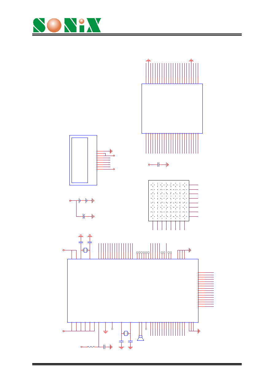
11.2 Application 2
3V/16M Crystal, with 1-Bit LCD driver (80 x 160) and 32M Flash memory
0
1
2
SPEAKER
3
(8 X 8 Matrix Key)
4
(3V Flash Memory)
6
5
2
_
0
7
8
10
9
11
VDD
12
14
13
1.5V
15
1.5V
VDD
Y1
32
76
8H
Z
C3
15
pF
C4
15
pF
VDD
2_
9
2_
8
2_
11
2_
10
2_
12
2_
14
2_
13
2_
15
C2
47uF
R1
220K
C7
0.1uF
VDD
160 X 80
U3
1-Bit LCM
LD0
LOAD
CP
FLM
AC
BLANK
POFF
VCC
GND
Y2
16MHZ
VDD
VDD
C5
15pF
C6
15pF
U2
MX29LV320T/B
A15
1
A14
2
A13
3
A12
4
A11
5
A10
6
A9
7
A8
8
A19
9
A20
10
WE_
11
RESET_
12
A21
13
WP_/ACC
14
RY/BY_
15
A18
16
A17
17
A7
18
A6
19
A5
20
A4
21
A3
22
A2
23
A1
24
A0
25
CE_
26
GND
27
OE_
28
Q0
29
Q8
30
Q1
31
Q9
32
Q2
33
Q10
34
Q3
35
Q11
36
Vcc
37
Q4
38
Q12
39
Q5
40
Q13
41
Q6
42
Q14
43
Q7
44
Q15/A-1
45
GND
46
BYTE_
47
A16
48
C1
0.1uF
VDD
U1
SNL310
VDD
3
VDD
19
VDD
37
VDD
48
CVDD
85
CVDD
26
GND
5
GND
17
GND
28
GND
41
GND
46
RST
83
BP0
47
BN0
49
VO
4
XIN
6
XOUT
7
LXIN
2
LXOUT
1
TESTM
53
CKSEL
52
P2.0
90
P2.1
89
P2.2
88
P2.3
87
P2.4
86
P2.5
82
P2.6
81
P2.7
80
P2.8
78
P2.9
77
P2.10
76
P2.11
75
P2.12
74
P2.13
73
P2.14
72
P2.15
71
GND
50
GND
84
P3.0
70
P3.1
69
P3.2
68
P3.3
67
P3.4
66
P3.5
65
P3.6
64
P3.7
63
P3.8
61
P3.9
59
P3.10
58
P3.11
57
P3.12
56
P3.13
55
P3.14
54
P3.15
51
P5.0
25
P5.1
24
P5.2
23
P5.3
22
P5.4
21
P5.5
20
P5.6
18
P5.7
16
P5.8
15
P5.9
14
P5.10
13
P5.11
12
P5.12
11
P5.13
10
P5.14
9
P5.15
8
P4.0
45
P4.1
44
P4.2
43
P4.3
42
P4.4
40
P4.5
39
P4.6
38
P4.7
36
P4.15
27
P4.14
29
P4.13
30
P4.12
31
P4.11
32
P4.10
33
P4.9
34
P4.8
35
VDD
60
VDD
79
D7
A
CE\
A
A
A
A
A
A
P
A
P2_1
A
P2_2
A
A
P2_3
A
P2_4
A
P2_5
A
P2_6
A
P2_7
A
P2_8
P2_9 P2_10
P2_11 P2_12
P2_13 P2_14
P2_15
P2_0
P2_1
P2_3
P2_2
P2_4
P2_5
P2_6
P2_7
P
P
P
P
P
P
P
P
RST
FRAME
COMD
LCO1
LCO2
LSD
LSD
A16
LCO1 LCO2
FRAME COMD
A17 A18
A19
BYTE\
A20
A0
GND
A17
VDD
D7
D6
D4
D5
D0
D3
D2
A1
GND
D1
A21
CE\
OE\
A13
A15 A14
A10
A9
A16
A11
A12
VDD
WR\RD
A21
A19
BUSY\
A20
VDD
A22
A7
A6
A8
A3
A18
A2
A5
A4
WR\RD
D0
D1 D2
D4
D3
D5 D6
Ver: 1.7
May 2, 2003
21
SNL310
16-Bit LCD Controller
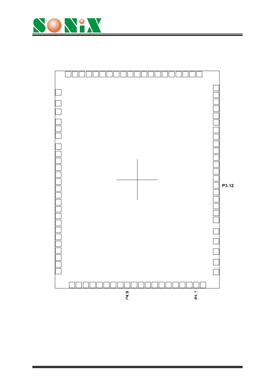
12. BONDING PAD
1
2
3
4
5
6
7
8
9
10
11
12
13
14
15
16
17
18
19
20
21
22
23
24
25
26 27 28 29 30 31 32 33 34 35 36 37 38 39 40 41 42 43 44 45
46
47
48
49
50
51
52
53
54
55
56
57
58
59
60
61
62
63
64
65
66
67
68
69
70
71
72
73
74
75
76
77
78
79
80
81
82
83
84
85
86
87
88
89
90
(0.00,0.00)
LXOUT
LXIN
VDD
VO
GND
XIN
XOUT
P5.15
P5.14
P5.13
P5.12
P5.11
P5.10
P5.9
P5.8
P5.7
GND
P5.6
VDD
P5.5
P5.4
P5.3
P5.2
P5.1
P5.0
CV
D
D
P4
.1
5
GND
P4
.
1
4
P4
.
1
3
P4
.1
2
P4
.1
1
P4
.
1
0
P4
.8
P4
.7
VD
D
P4
.6
P4
.5
P4
.
4
GND
P4
.3
P4.2
P4
.0
GND
BP0
VDD
BN0
GND
P3.15
CKSEL
TESTM
P3.14
P3.13
P3.11
P3.10
P3.9
VDD
P3.8
GND
P3.7
P3.6
P3.5
P3.4
P3.3
P3.2
P3.1
P3.0
P2
.
1
5
P2
.
1
4
P2
.
1
3
P2
.
1
2
P2
.
1
1
P2
.
1
0
P2
.
9
P2
.
8
VD
D
P2
.
7
P2
.
6
P2
.
5
RS
T
GN
D
CV
D
D
P2
.
4
P2
.
3
P2
.
2
P2
.
1
P2
.
0
Note: The substrate MUST be connected to Vss in PCB layout.
Ver: 1.7
May 2, 2003
22
SNL310
16-Bit LCD Controller
13. ABSOLUTE MAXIMUM RATINGS
Items
Symbol
Min
Max
Unit.
Supply Voltage
V
DD
-V -0.3 6.0
V
Input Voltage
V
IN
GND-0.3
V
DD
+0.3 V
Operating Temperature
T
OP
0 55
o
C
Storage Temperature
T
STG
-55.0 125.0
o
C
14. ELECTRICAL CHARACTERISTICS
Item
Sym. Min. Typ. Max. Unit
Condition
Operating Voltage
V
DD
2.4 - 3.6 V
*1.
V
DD
3.6 - 5.1 V
*2.
Standby current
I
SBY
- - 2.0 uA V
DD
=3V, no load
Operating Current
I
OPR
- - 5 mA
V
DD
=3V, no load
Input current of P2, P3, P4,
P5
I
IH
- - 10.0
uA V
DD
=3V,V
IN
=3V
Drive current of P2, P3, P4,
P5
I
OD
- 10 - mA V
DD
=3V,V
O
=2.4V
Sink Current of P2, P3, P4,
P5
I
OS
- 12 - mA V
DD
=3V,V
O
=0.4V
Drive current of Buo1
I
OD
100 120 - mA V
DD
=3V,Buo1=1.5V
Sink Current of Buo1
I
OS
100 120 - mA V
DD
=3V,Buo1=1.5V
Drive Current of Buo2
I
OD
100 120 - mA V
DD
=3V,Buo2=1.5V
Sink Current of Buo2
I
OS
100 120 - mA V
DD
=3V,Buo2=1.5V
Oscillation Freq. (crystal)
F
OSC
- 16.0 - MHz
V
DD
=3V
Note:
1. For 2 batteries application.
2. For 3 batteries application, user should add 1 resister between power and
CVDD pin of chip.
Ver: 1.7
May 2, 2003
23

SNL310
16-Bit LCD Controller
Ver: 1.7
May 2, 2003
24
DISCLAIMER
The information appearing in SONiX web pages ("this publication") is believed to be
accurate.
However, this publication could contain technical inaccuracies or typographical errors.
The reader should not assume that this publication is error-free or that it will be
suitable for any particular purpose. SONiX makes no warranty, express, statutory
implied or by description in this publication or other documents which are referenced
by or linked to this publication. In no event shall SONiX be liable for any special,
incidental, indirect or consequential damages of any kind, or any damages whatsoever,
including, without limitation, those resulting from loss of use, data or profits, whether or
not advised of the possibility of damage, and on any theory of liability, arising out of or
in connection with the use or performance of this publication or other documents which
are referenced by or linked to this publication.
This publication was developed for products offered in Taiwan. SONiX may not offer
the products discussed in this document in other countries. Information is subject to
change without notice. Please contact SONiX or its local representative for
information on offerings available. Integrated circuits sold by SONiX are covered by
the warranty and patent indemnification provisions stipulated in the terms of sale only.
The application circuits illustrated in this document are for reference purposes only.
SONIX DISCLAIMS ALL WARRANTIES, INCLUDING THE WARRANTY OF
MERCHANTABILITY OR FITNESS FOR ANY PURPOSE. SONIX reserves the right
to halt production or alter the specifications and prices, and discontinue marketing the
Products listed at any time without notice. Accordingly, the reader is cautioned to
verify that the data sheets and other information in this publication are current before
placing orders.
Products described herein are intended for use in normal commercial applications.
Applications involving unusual environmental or reliability requirements, e.g. military
equipment or medical life support equipment, are specifically not recommended
without additional processing by SONIX for such application.