 | –≠–ª–µ–∫—Ç—Ä–æ–Ω–Ω—ã–π –∫–æ–º–ø–æ–Ω–µ–Ω—Ç: 3SK166A-0 | –°–∫–∞—á–∞—Ç—å:  PDF PDF  ZIP ZIP |
Description
The 3SK166A is an N-channel dual gate GaAs
MES FET for UHF band low-noise amplification. The
circuit matching is easier to be made for all UHF
band, resulting in the excellent performance, due to
the optimal design of input impedance.
Features
∑ Low voltage operation
∑ Low noise: NF = 1.2dB (typ.) at 800MHz
∑ High gain: Ga = 20dB (typ) at 800MHz
∑ High stability
Application
UHF band amplifier, oscillator
Structure
GaAs N-channel dual-gate metal semiconductor field-effect transistor
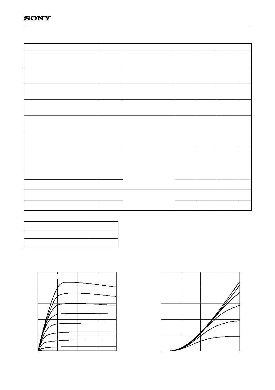
Absolute Maximum Ratings (Ta = 25∞C)
∑ Drain to source voltage
V
DSX
8
V
∑ Gate 1 to source voltage
V
G1S
≠6
V
∑ Gate 2 to source voltage
V
G2S
≠6
V
∑ Drain current
I
D
80
mA
∑ Allowable power dissipation
P
D
150
mW
∑ Channel temperature
Tch
150
∞C
∑ Storage temperature
Tstg
≠55 to +150
∞C
≠ 1 ≠
3SK166A
E96Y11-PS
GaAs N-channel Dual Gate MES FET
Sony reserves the right to change products and specifications without prior notice. This information does not convey any license by
any implication or otherwise under any patents or other right. Application circuits shown, if any, are typical examples illustrating the
operation of the devices. Sony cannot assume responsibility for any problems arising out of the use of these circuits.
For the availability of this product, please contact the sales office.
≠ 2 ≠
3SK166A
≠2.0
≠1.5
≠1.0
≠0.5
0
20
60
70
80
100
(V
DS
= 5V)
V
G2S
= 1.5V
1.0V
0.5V
0V
≠0.5V
≠1.5V
40
0
2
4
6
8
0
20
40
60
100
V
G1S
= 0V
≠0.4V
≠0.6V
≠0.8V
≠1.4V
≠1.6V
80
≠0.2V
≠1.0V
≠1.2V
(V
G2S
= 1.5V)
V
G1S
≠ Gate 1 to source voltage [V]
I
D
≠ Drain current [mA]
I
D
vs. V
G1S
V
DS
≠ Drain to source voltage [V]
I
D
≠ Drain current [mA]
I
D
vs. V
DS
Typical Characteristics (Ta = 25∞C)
Electrical Characteristics
(Ta = 25∞C)
Item
Drain cut-off current
Gate 1 to source current
Gate 2 to source current
Drain saturation current
Gate 1 to source cut-off voltage
Gate 2 to source cut-off voltage
Forward transfer admittance
Input capacitance
Feedback capacitance
Noise figure
Associated gain
I
DSX
I
G1SS
I
G2SS
I
DSS
V
G1S
(OFF)
V
G2S
(OFF)
gm
Ciss
Crss
NF
Ga
V
DS
= 8V
V
G1S
= ≠4V
V
G2S
= 0V
V
G1S
= ≠5V
V
G2S
= 0V
V
DS
= 0V
V
G2S
= ≠5V
V
G1S
= 0V
V
DS
= 0V
V
DS
= 5V
V
G1S
= 0V
V
G2S
= 0V
V
DS
= 5V
I
D
= 100µA
V
G2S
= 0V
V
DS
= 5V
I
D
= 100µA
V
G1S
= 0V
V
DS
= 5V
I
D
= 10mA
V
G2S
= 1.5V
f = 1kHz
V
DS
= 5V
I
D
= 10mA
V
G2S
= 1.5V
f = 1MHz
V
DS
= 5V
I
D
= 10mA
V
G2S
= 1.5V
f = 800MHz
20
≠1
≠1
25
18
40
1.3
25
1.2
20
100
≠20
≠20
80
≠4
≠4
2.0
40
2.5
µA
µA
µA
mA
V
V
ms
pF
fF
dB
dB
Symbol
Condition
Min.
Typ.
Max.
Unit
I
DSS
classification
Product name classification
3SK166A-0
3SK166A-2
I
DSS
RANK
20 to 80mA
45 to 80mA
≠ 3 ≠
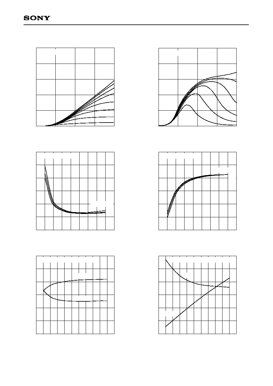
3SK166A
NF vs. V
G1S
Ga vs. V
G1S
≠2.0
≠1.5
≠1.0
≠0.5
0
0
40
60
80
100
(V
DS
= 5V)
V
G1S
= 0V
≠0.4V
≠0.6V
≠1.0V
≠1.2V
≠1.4V
≠0.2V
≠0.8V
20
≠2.0
≠1.5
≠1.0
≠0.5
0
20
50
60
80
100
(V
DS
= 5V)
V
G2S
= 1.5V
1.0V
0.5V
0V
≠0.5V
40
≠1.0V
≠1.8
≠1.6
≠1.4
≠1.2
≠1.0 ≠0.9
0
2
3
4
6
(V
DS
= 5V, f = 800MHz)
1
≠1.7
≠1.5
≠1.3
≠1.1
5
V
G2S
= 0.5V
1.0V
1.5V
0
4
8
12
16
20 22
0
1.0
1.5
2.5
3.0
(V
DS
= 5V, V
G2S
= 1.5V, f = 800MHz)
0.5
2
6
10
14
2.0
18
0
10
15
25
30
5
20
Ga
NF
0
0.8
1.6
2.2
0
1.0
1.5
2.5
3.0
0.5
0.4
1.2
2.0
2.0
0
10
15
25
30
5
20
(V
DS
= 5V, V
G2S
= 1.5V, I
D
= 10mA)
Ga
NFmin
0.6
1.4
0.2
1.0
1.8
0
10
15
25
30
5
20
V
G2S
= 1.5V
(V
DS
= 5V, f = 800MHz)
≠1.8
≠1.6
≠1.4
≠1.2
≠1.0 ≠0.9
≠1.7
≠1.5
≠1.3
≠1.1
1.0V
1.5V
V
G2S
≠ Gate 2 to source voltage [V]
I
D
≠ Drain current [mA]
I
D
vs. V
G2S
V
G1S
≠ Gate 1 to source voltage [V]
gm ≠ Forward transfer admittance [ms]
gm vs. V
G1S
f ≠ Frequency [GHz]
NFmin ≠ Minimum noise figure [dB]
NF, Ga vs. f
Ga ≠ Gain [dB]
V
G1S
≠ Gate 1 to source voltage [V]
NF ≠ Noise figure [dB]
V
G1S
≠ Gate 1 to source voltage [V]
Ga ≠ Gain [dB]
I
D
≠ Drain current [mA]
NF ≠ Noise figure [dB]
NF, Ga vs. I
D
Ga ≠ Gain [dB]
≠ 4 ≠
3SK166A
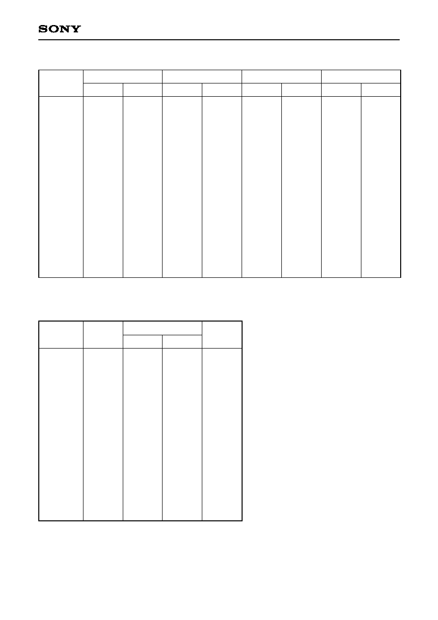
S-parameter vs. Frequency Characteristics (V
DS
= 5V, V
G2S
= 1.5V, I
D
= 10mA)
(Z
0
= 50
)
f
(MHz)
100
200
300
400
500
600
700
800
900
1000
1100
1200
1300
1400
1500
1600
1700
1800
1900
2000
0.936
0.933
0.930
0.927
0.925
0.922
0.923
0.921
0.926
0.924
0.920
0.921
0.921
0.924
0.925
0.926
0.927
0.924
0.915
0.912
≠1.9
≠4.0
≠6.1
≠8.2
≠10.2
≠12.1
≠14.2
≠16.3
≠18.2
≠20.3
≠22.3
≠24.4
≠26.5
≠28.9
≠31.4
≠33.9
≠36.9
≠39.5
≠42.4
≠45.0
S22
MAG
ANG
0.002
0.005
0.007
0.009
0.010
0.011
0.013
0.013
0.015
0.016
0.016
0.016
0.017
0.017
0.018
0.018
0.020
0.022
0.026
0.028
86.5
87.7
87.3
85.6
81.9
84.3
83.5
82.3
86.3
86.8
88.0
92.4
95.8
97.9
103.3
111.5
119.2
129.3
132.1
136.6
S12
MAG
ANG
3.807
3.783
3.726
3.670
3.602
3.507
3.414
3.333
3.244
3.146
3.061
2.965
2.874
2.800
2.709
2.636
2.545
2.464
2.364
2.283
172.8
165.5
158.4
151.5
144.5
137.9
131.4
125.2
118.9
112.8
106.9
101.2
95.4
90.0
84.2
78.5
72.8
67.0
61.3
55.8
S21
MAG
ANG
0.996
0.988
0.969
0.948
0.927
0.899
0.873
0.845
0.816
0.785
0.754
0.723
0.694
0.669
0.643
0.621
0.601
0.583
0.565
0.545
≠5.0
≠9.8
≠14.8
≠19.8
≠24.6
≠29.3
≠33.5
≠37.5
≠41.2
≠44.5
≠47.6
≠50.3
≠53.2
≠55.6
≠58.1
≠60.4
≠62.3
≠64.5
≠66.6
≠68.1
S11
MAG
ANG
Noise Figure Characteristics (V
DS
= 5V, V
G2S
= 1.5V, I
D
= 10mA)
f
(MHz)
200
300
400
500
600
700
800
900
1000
1100
1200
1300
1400
1500
1600
1700
1800
1900
2000
7.3
10.6
13.7
16.7
19.5
22.3
24.9
27.5
30.1
32.6
35.2
37.8
40.5
43.3
46.3
49.3
52.6
56.0
59.7
30.3
29.7
29.2
28.7
28.3
27.8
27.4
27.0
26.7
26.3
26.0
25.8
25.5
25.3
25.1
25.0
24.9
24.8
24.7
MAG
Rn
(
)
0.29
0.41
0.52
0.64
0.75
0.86
0.97
1.07
1.18
1.28
1.39
1.49
1.59
1.68
1.78
1.88
1.97
2.06
2.15
0.89
0.85
0.81
0.77
0.73
0.70
0.67
0.64
0.61
0.59
0.57
0.54
0.52
0.50
0.48
0.45
0.43
0.40
0.38
Gamma Optimum
NFmin
(dB)
ANG

≠ 5 ≠
3SK166A
Package Outline
Unit: mm
M-254
SONY CODE
EIAJ CODE
JEDEC CODE
M-254
PACKAGE MASS
0.01g
2.9 ± 0.2
1.9
( 0.95 )
( 0.95 )
1.1 ≠ 0.1
+ 0.2
0.6
2.8 ±
0.2
1.6 ≠ 0.1
+ 0.2
1.8
( 0.85 )
( 0.95 )
0 to 0.1
0.10 ≠ 0.01
+ 0.1
0.6 ≠ 0.05
+ 0.1
0.4 ≠ 0.05
+ 0.1
1
2
3
4
1. Source
2. Gate1
3. Gate2
4. Drain