Description
The CXA2550M/N is an IC developed for compact
disc players. This IC incorporates an RF amplifier,
focus error amplifier, tracking error amplifier, APC
circuit and RF level control circuit. (The voltage-
converted optical pickup output is supported.)
Features
∑ Low power consumption (35mW at 3.5V)
∑ APC circuit
∑ RF level control circuit
∑ Both single power supply and dual power supply
operations possible.
Structure
Bipolar silicon monolithic IC
Applications
Compact disc players
Absolute Maximum Ratings (Ta = 25∞C)
∑ Supply voltage
V
CC
12
V
∑ Operating temperature Topr
≠20 to +75
∞C
∑ Storage temperature
Tstg
≠65 to +150
∞C
∑ Allowable power dissipation
P
D
(SOP)
620
mW
(SSOP) 370
mW
Operating Conditions
Supply voltage
V
CC
≠ V
EE
3.0 to 4.0
V
≠ 1 ≠
CXA2550M/N
E97514B25
RF Amplifier for CD Players
Sony reserves the right to change products and specifications without prior notice. This information does not convey any license by
any implication or otherwise under any patents or other right. Application circuits shown, if any, are typical examples illustrating the
operation of the devices. Sony cannot assume responsibility for any problems arising out of the use of these circuits.
CXA2550M
20 pin SOP (Plastic)
CXA2550N
20 pin SSOP (Plastic)
10
15
17
20
VC
VC
10k
8k
6p
VC
VC
10k
8k
6p
4
5
2k
2k
VC
13.4k
V
CC
50µ
A
10k
56k
10k
V
EE
10k
55k
10k
56k
1k
V
CC
V
EE
APC LD
AMP
APC PD AMP
VREF 1.25V
V
CC
19
18
15k
VC
54k
V
EE
6k
16
VC
2k
2k
VC
13k
12p
V
EE
VC
25k
260k
260k
26k
13k
12p
VC
VC
6
7
9
32k
32k
24p
174k
13
14
24p
87k
154k
FOCUS
ERROR
AMP
30k
30k
96k
11
12
TRACKING
ERROR
AMP
15k
49
VC
V
CC
30k
30k
V
EE
2
3
1
AGCVTH
LD
PD
PD1
PD2
V
EE
F
E
EI
VC
V
CC
LD_ON
AGCCONT
(50%/30%/OFF)
RFTC
RF I
RF O
RFM
FE
FE_BIAS
TE
8
95k
VC
VC
670mV
Block Diagram and Pin Configuration (Top View)

≠ 2 ≠
CXA2550M/N
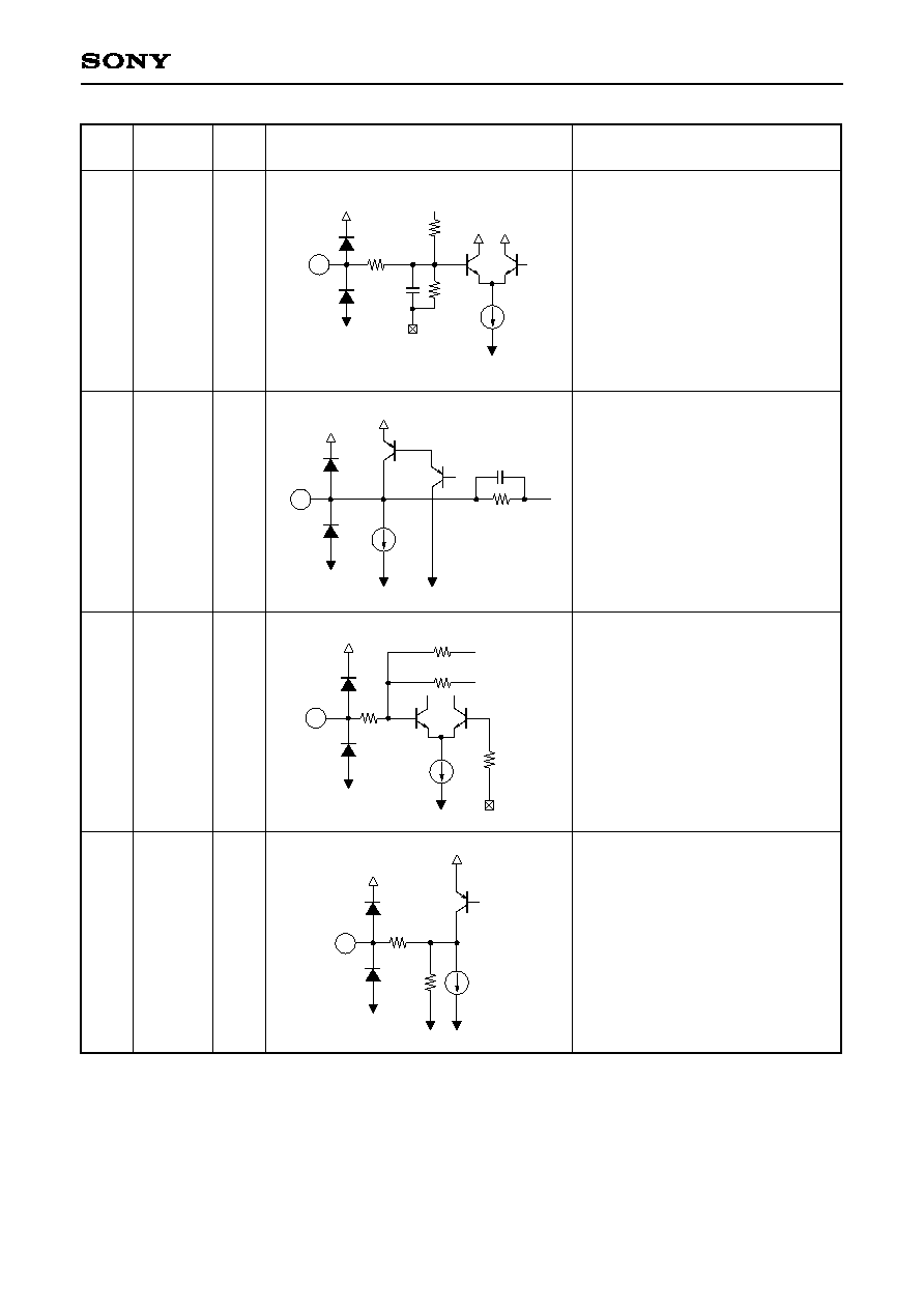
Pin Description
Pin
No.
Symbol
I/O
Equivalent circuit
Description
1
AGCVTH
--
Reference level variable pin for RF
level control.
The reference level can be varied by
the external resistor.
147
13.4k
50µ
10µ
1
2
LD
O
APC amplifier output pin.
4
5
PD1
PD2
I
I
Inversion input pin for RF I-V
amplifiers.
Connect these pins to the
photodiodes A + C and B + D
respectively. The current is supplied.
2
10k
1k
3
PD
I
APC amplifier input pin.
55k
147
3
10k
20µ
8µ
10k
4
5
100µ
6
V
EE
--
6
V
EE
V
EE
pin.

≠ 3 ≠
CXA2550M/N
7
8
F
E
I
I
Inversion input pin for F and E I-V
amplifiers.
Connect these pins to the
photodiodes F and E respectively.
The current is supplied.
260k
10µ
7
8
12p
9
EI
--
Gain adjustment pin for I-V amplifier.
11
TE
O
Tracking error amplifier output pin.
E-F signal is output.
147
260k
26k
13k
9
10
VC
O
DC voltage output pin of
(Vcc + V
EE
)/2.
Connect to GND for ±1.75 power
supply; connect a smoothing
capacitor for single +3.5V power
supply.
50
200µ
10
120
120
16k
V
CC
V
CC
15k
V
EE
96k
300µ
11
Pin
No.
Symbol
I/O
Equivalent circuit
Description

≠ 4 ≠
CXA2550M/N
12
FE_BIAS
I
Bias adjustment pin for inverted side
of focus error amplifier.
164k
10µ
24p
32k
174k
12
13
FE
O
Focus error amplifier output pin.
15
RF O
O
RF amplifier output pin.
174k
300µ
13
24p
14
RFM
I
RF amplifier inverted side input pin.
RF amplifier gain is determined by
the resistor connected between this
pin and RFO pin.
2k
1m
2k
147
850
14
15
147
60k
1m
Pin
No.
Symbol
I/O
Equivalent circuit
Description

≠ 5 ≠
CXA2550M/N
16
RF I
I
The RF amplifier output RFO is input
with its capacitance coupled.
147
15k
20µ
16
17
RFTC
--
External time-constant pin for RF
level control.
19
LD_ON
I
APC amplifier ON/OFF switching
pin.
OFF for Vcc and ON for V
EE
.
147
50µ
10µ
17
50µ
18
AGCCONT
I
RF level control ON (limit level of
50%/30%)/OFF switching pin.
OFF for Vcc, 30% for open or Vc
and 50% for V
EE
.
147
50k
15µ
15µ
7µ
18
147
50µ
V
REF
19
20
V
CC
V
CC
20
Vcc pin.
Pin
No.
Symbol
I/O
Equivalent circuit
Description


