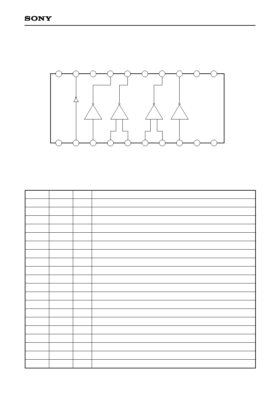
Description
CXD1250M/N is a clock driver developed for the
vertical register drive of CCD Image sensor.
Features
4-channel vertical clock driver and 1 channel
substrate driver are built-in.
Application
CCD camera
Structure
CMOS
Absolute Maximum Ratings (Ta = 25∞C)
∑ Supply voltage
V
DD
V
L
≠ 0.3 to V
L
+ 35.0
V
V
M
V
L
≠ 0.3 to V
L
+ 35.0
V
V
H
V
L
≠ 0.3 to V
L
+ 35.0
V
V
HH
V
L
≠ 0.3 to V
L
+ 35.0
V
∑ Input volltage
V
I
V
L
≠ 0.3 to V
DD
+ 0.3
V
∑ Output voltage
MV
(pins 13, 17)
V
L
≠ 0.3 to V
M
+ 0.3
V
∑ Output voltage
HV
(pins 14, 16)
V
L
≠ 0.3 to V
H
+ 0.3
V
∑ Output voltage
HHV
(pin 19)
V
L
≠ 0.3 to V
HH
+ 0.3
V
∑ Operating temperature
Topr
≠25 to +85
∞C
∑ Storage temperature
Tstg
≠40 to +125
∞C
Recommended Operating Conditions
∑ Supply voltage
V
DD
5.0 ± 0.5
V
V
M
V
L
+ 10.0
V
V
H
V
L
+ 25.0
V
V
HH
V
L
+ 30.0
V
V
L
≠10.0
V
∑ Operating temperature
Topr
≠20 to +75
∞C
≠ 1 ≠
CXD1250M/N
80639C43-PK
Vertical Clock Driver for CCD Image sensor
Sony reserves the right to change products and specifications without prior notice. This information does not convey any license by
any implication or otherwise under any patents or other right. Application circuits shown, if any, are typical examples illustrating the
operation of the devices. Sony cannot assume responsibility for any problems arising out of the use of these circuits.
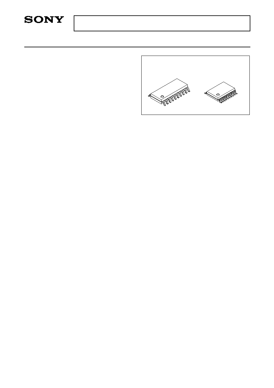
CXD1250M
20 pin SOP (Plastic)
CXD1250N
20 pin SSOP (Plastic)
≠ 3 ≠
CXD1250M/N
Truth Table
DC Characteristics (Ta = 25∞C)
Input
XV1 ∑ 3
L
H
X
X
X
X
L
H
H
H
X
X
X
X
L
L
X
X
L
H
X
X
X
X
X
X
X
X
L
H
X
X
V
M
V
L
X
X
X
X
V
H
Z
X
X
V
M
V
L
X
X
X
X
X
X
X
X
V
HH
V
L
X
X
XSG1 ∑ 2
XV2 ∑ 4
Xsub
V
1 ∑ 3
V
2 ∑ 4
Vsub
Output
X : Don't care
Z : High impedance
Item
"H" level input voltage
"L" level input voltage
"L" level output voltage
"M" level output voltage
"M" level output voltage
"H" level output voltage
"HH" level output voltage
Input current
Power supply current
Power supply current
Power supply current
Power supply current
V
IH
V
IL
V
L
V
M
V
M
V
H
V
HH
Ii
I
M
I
DD
I
H
I
HH
I
L
= 20µA
I
M
= ≠20µA
I
M
= 20µA
I
H
= ≠20µA
I
HH
= ≠20µA
3.5
--
--
--
≠0.1
14.9
19.9
--
--
--
--
--
--
--
≠10
0.0
0.0
15
20
1.0
4.5
0.3
0.1
0.05
--
1.5
≠9.9
0.1
--
--
--
--
5.0
0.5
0.2
0.1
V
V
V
V
V
V
V
µA
mA
mA
mA
mA
V
DD
= 5V
V
L
= ≠10V
V
M
= 0V
V
H
= 15V
V
HH
= 20V
Symbol
Min.
Typ.
Max.
Unit
Test condition
Power supply
Suuply current at operation (See the Test Circuit)

≠ 4 ≠
CXD1250M/N
Switching Characteristics (See the Test Circuit Ta = 25∞C, V
HH
= 20V, V
H
= 15V, V
M
= 0V, V
L
= ≠10V, V
DD
= 5V)
Item
Output current
Output current
Output current
Output current
Output current
Output current
Rise time V
L
V
M
Fall time V
M
V
L
Rise time V
M
V
H
Fall time V
H
V
M
Rise time V
L
V
HH
Fall time V
HH
V
L
Coupling amplitude (middle level)
Coupling amplitude (low level)
I
L
I
M1
I
M2
I
H
I
SL
I
SH
T
TLM
T
TML
T
TMH
T
THM
T
TLHH
T
THHL
V
COM
V
COL
V
1 to 4 = ≠9.5V
V
1 to 4 = ≠0.5V
V
1, 3 = 0.5V
V
1, 3 = 14.5V
Vsub = ≠9.5V
Vsub = ≠19.5V
V
1 to 4 = ≠0.5V
After input transient
V
1 to 4 = ≠9.5V
After input transient
V
1, 3 = 14V
After input transient
V
1, 3 = 1V
After input transient
Vsub = 17V
After input transient
Vsub = ≠7V
After input transient
V
1 to 4
V
1 to 4
≠25
≠9
≠12
1000
500
1000
1000
200
200
0.5
0.5
10
12
7
mA
mA
mA
mA
mA
mA
ns
ns
ns
ns
ns
ns
V
V
Symbol
Conditions
Max.
Min.
Unit
Input Waveform (Repeat Cycle 15.7kHz)
Output Waveform
600ns
XV1
5
0
XV2
5
0
XV3
5
0
XV4
5
0
T
TML
T
TLM
V
COM
V
COL
V
1
0
0
≠10
V
2
V
3
≠10
0
≠10
0
≠10
V
4