 | –≠–ª–µ–∫—Ç—Ä–æ–Ω–Ω—ã–π –∫–æ–º–ø–æ–Ω–µ–Ω—Ç: CXA1511L | –°–∫–∞—á–∞—Ç—å:  PDF PDF  ZIP ZIP |

Preamplifier for Remote Control Signal Reception
Description
The CXA1511L/M is a bipolar IC used for
preamplifiers that receive signals in infrared remote
control systems. These ICs consist of a first-stage
amplifier, limiter amplifier, band-pass filter, band
elimination filter, signal waveform detection circuit
and waveform shaping circuit.
Features
∑ Low power consumption (V
CC
= 5V, 9mW typ.)
∑ Low supply voltage (V
CC
= 5V)
∑ Filters (center frequency can be varied through
external resistor: fo = 30kHz to 60kHz, 40kHz typ.)
∑ Elimination of inductors prevents magnetic field
inductance interference.
∑ Optical reception diode can be coupled directly.
∑ Collector output (pull-up resistor, TTL and CMOS
can be connected directly)
Applications
TVs, VCRs, audio equipment
Structure
Bipolar silicon monolithic IC
Block Diagram and Pin Configuration
Absolute Maximum Ratings
∑ Supply voltage
V
CC
7
V
∑ Operating temperature
Topr ≠20 to +75
∞C
∑ Storage temperature
Tstg ≠65 to +150
∞C
∑ Allowable power dissipation
P
D
600
mW (SIP)
∑ Allowable power dissipation
P
D
300 mW (SOP)
Operating Conditions
∑ Supply voltage
4.7 to 5.3
V
≠ 1 ≠
E94301A8X
Sony reserves the right to change products and specifications without prior notice. This information does not convey any license by
any implication or otherwise under any patents or other right. Application circuits shown, if any, are typical examples illustrating the
operation of the devices. Sony cannot assume responsibility for any problems arising out of the use of these circuits.
CXA1511L/M
8 pin SIP (Plastic)
8 pin SOP (Plastic)
4
6
8
1
2
7
3
5
C1
C2 GND fo N.C.
V
CC
OUT
470, 680
0.01µ
0.01µ
V
CC
= 5V
200k
(fo = 40kHz)
Hysteresis
Comparator
Delector &
Comparator Integralor
BPF
BEF
Limiter
Amp
Head
Amp
IN
Photo
Diode
ABLC

≠ 2 ≠
CXA1511L/M
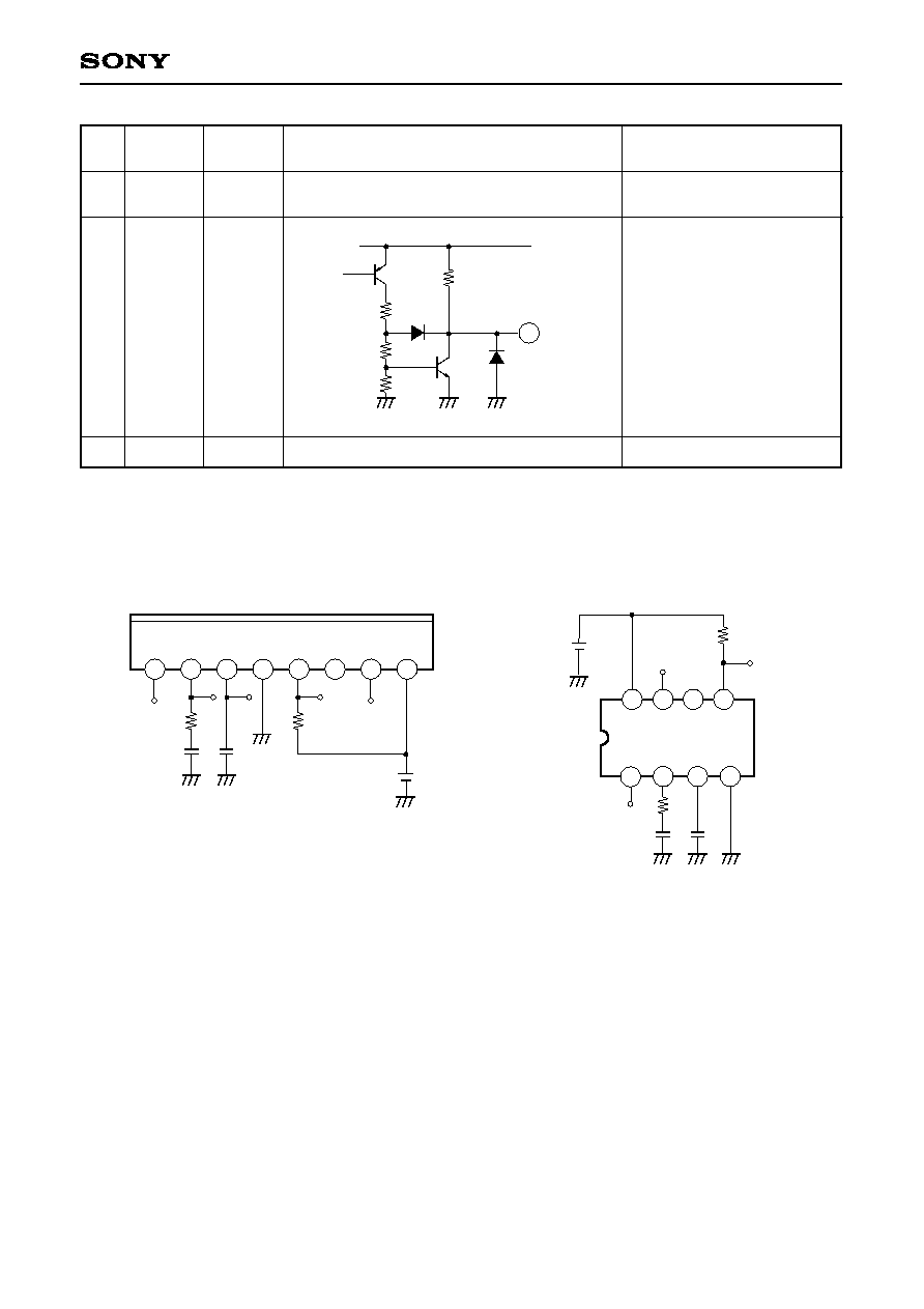
Pin Description
Pin voltage depends on the DC Characteristics Measurement Circuit.
Pin
No.
Symbol
Pin
voltage
Equivalent circuit
Description
1
2
IN
C1
2.8V
2.8V
Input pin.
Connect optical reception
diode to GND.
Connect a resistor and
capacitor in series to GND,
and set the frequency
response and gain of "Head
Amp".
When the resistor is large
and the capacitor small, the
gain is small.
When the capacitor is large,
sensitivity decreases in
relation to the transient
response.
3
C2
1.9V
Connect a detection capacitor
to GND.
When the capacitor is large,
sensitivity decreases in relation
to the mean value detection
and transient response.
When the capacitor is small,
fluctuation of the peak detection
and output pulse width
increases.
The capacitor in usage is
0.01µF (typ.). Set output pulse
width fluctuation and noise
elimination characteristics to be
optimum.
4
GND
GND pin.
Adopt a pattern design that will
allow external parts to be
located as closely as possible
to this pin. Ground them all at
the same point. The transport
distance and noise elimination
characteristics are greatly
influenced by the pattern design
surrounding the GND.
5
fo
1.4V
Connect a resistor to the
power supply.
Set the center frequency of
the built-in BPF.
See "External resistor at
Pin 5 vs. Center frequency
response" on Page 6.
V
CC
40µA
V
CC
47k
160k
8k
40µA
8k
1
2
V
CC
330k
30µA
8k
30nA
3
V
CC
V
CC
8k
4p
5
≠ 3 ≠
CXA1511L/M
Pin
No.
Symbol
Pin
voltage
Equivalent circuit
Description
6
7
8
N.C.
OUT
V
CC
5.0V
(High)
0.6V
(Low)
5.0V
No connected pin.
Connect to GND.
Output pin.
Supply voltage pin.
V
CC
24k
30k
14k
30k
7
DC Characteristics Measurement Circuit
(CXA1511L)
(CXA1511M)
2
3
4
5
6
7
8
6
1
2
3
4
5
7
8
CXA1511L
470
0.01µ
200k
CXA1511M
0.01µ
200k
5V
0.01µ
1
5V
0.01µ
470
≠ 4 ≠
CXA1511L/M
Item
Input pin voltage (1)
Input pin voltage (2)
L level output voltage
Voltage gain
BPF characteristics (1)
BPF characteristics (2)
Input impedance
Detecting ability
Current consumption
V
IN
1
V
IN
2
V
OL
A
V
A
VQ1
A
VQ2
r
in
Det
Icc
40kHz CW
30kHz, 37kHz CW
40kHz, 48kHz CW
40kHz CW
burst wave
30
µ
Vp-p
40
µ
Vp-p
40
µ
Vp-p
200mVp-p
60
µ
Vp-p
S1, 3, 7
S1, 2, 3, 4, 7
S3, 7, 8
S2, 5, 6, 9
S2, 5, 6, 9
S2, 5, 6, 9
S1, 2, 6, 7
S2, 5, 6, 7
S3, 7
A
A
C
B
B
B
A
C
D
2.3
0.6
--
75
5
5
31
440
1.0
2.8
1.2
0.6
81
10
19
40
550
1.8
3.3
1.8
1.3
85
--
--
64
770
2.8
V
V
V
dB
dB
dB
k
µ
s
mA
100
µ
A is flown out from Pin 1.
Note 1)
Note 2)
Note 3)
Input level is taken Vi and
measuring value is taken Vx.
Burst wave signal with a
1.2ms, 40kHz cycle is input.
1
2
3
4
5
6
7
8
9
Symbol
Measurement
point
Min.
Typ.
Max.
Unit
Remarks
Measurement condition
Signal
Level
ON-SW
Electrical Characteristics
(V
CC
= 5V, Ta = 25
∞
C)
Note 1) The level ratio between AC level at 37kHz and that at 30kHz is taken A1 [dB].
A1=20log
measuring value (f = 37kHz)
measuring value (f = 30kHz)
Note 2) The level ratio between AC level at 40kHz and that at 48kHz is taken A2 [dB].
A2=20log
measuring value (f = 40kHz)
measuring value (f = 48kHz)
47k
Note 3) rin= [k
]
(Vi/Vx) ≠1)
No.

≠ 5 ≠
CXA1511L/M
Electrical Characteristics Measurement Circuit
Application Circuit
(CXA1511L)
(CXA1511M)
Description of Operation (See the Block Diagram.)
Receives infrared signals transmitted from the infrared remote control commander with a photodiode to output
them as rectangular waves.
5
6
7
2
A
1
3
4
8
C
D
B
470
0.01µ
E2
5.0V
200k
330k
E1
1.0V
0.01µ
S9
S8
S7
SG
S6
S3
S2
S1
0.47µ
S5
0.47µ
50
I1
100µA
S4
R
6
4
7
k
1
3
4
5
6
7
8
6
1
2
3
4
5
7
8
CXA1511L
Photo
Diode
PH302B
470,
680
0.01µ
200k
1%
(fo = 40kHz)
OUT
47
47µ
+5V
470,
680
CXA1511M
Photo
Diode
PH302B
OUT
200k
1%
(fo = 40kHz)
+5V
0.01µ
2
0.01µ
0.01µ
47
47µ
600µs
typ.
40kHz (typ.)
40µVp-p
to 2.5Vp-p
5V
0.6V
(typ.)
I/O pin
Waveform
Operation
Pin 1
Input waveform
Pin 3
BPF output
waveform
Hysteresis
comparator
input waveform
Pin 7
Output
waveform
Converts the signal current of a photodiode into
voltage and amplifies it.
Suppresses the noise component with BPF and
BEF.
Detects the signal component and performs
wave detection.
Integrates the signal component and outputs it
as rectangular wave from the hysteresis
comparator.

≠ 6 ≠
CXA1511L/M
Example of Representative Characteristics
V
CC
vs. I
CC
characteristics
I
C
C
[
m
A
]
2.0
1.5
1.0
4.0
5.0
6.0
V
CC
[V]
Ta = 25∞C
External resistor at Pin 2 vs.
A
V
1 characteristics
100
1k
10k
0
≠5
≠10
≠15
≠20
External resistor at Pin 2 [
]
B
P
F
r
e
l
a
t
i
v
e
v
o
l
t
a
g
e
g
a
i
n
[
d
B
]
(
P
i
n
3
)
V
IN
= 50µVp-p
(Pin 1)
f = 40kHz
Ta = 25∞C
V
CC
= 5V
I1 vs. V
IN
2 characteristics
I1 [µA]
1
10
100
4
3
2
1
0
V
I
N
2
[
V
]
Ta = 25∞C
V
CC
= 5V
External resistor at Pin 5 vs.
Center frequency response
C
e
n
t
e
r
f
r
e
q
u
e
n
c
y
[
k
H
z
]
100
80
60
40
20
0
100
200
300
External resistor at Pin 5 [k
]
400
0
Ta = 25∞C
V
CC
= 5V
V
IN
= 50µVp-p
(Pin 1)
80
70
60
50
40
30
10
20
100
f vs. A
V
1 characteristics
30 40
f [kHz]
A
v
1
[
d
B
]
Ta = 25∞C
V
CC
= 5V
0.5
10µ
100m
100µ
1m
10m
1
5
B
P
F
o
u
t
p
u
t
(
P
i
n
3
)
Input voltage at Pin 1 vs.
Output voltage at Pin 3 characteristics
V
IN
[Vp-p] (Pin 1 input)
0.1
f = 40kHz
Ta = 25∞C
V
CC
= 5V

≠ 7 ≠
CXA1511L/M
SONY CODE
EIAJ CODE
JEDEC CODE
PACKAGE STRUCTURE
PACKAGE MATERIAL
LEAD TREATMENT
LEAD MATERIAL
PACKAGE MASS
EPOXY RESIN
SOLDER PLATING
COPPER ALLOY
19.0 ≠ 0.2
+ 0.5
2.54
1
0.5 ± 0.1
1.2 ≠ 0.1
+ 0.3
8
3
.
0
6
.
4
≠
0
.
2
1
.
2
M
I
N
8
.
3
M
A
X
0.25 ≠ 0.05
+ 0.1
1.2 ± 0.1
SIP-8P-02
SIP008-P-0340
+
0
.
5
2.8 ± 0.2
0.7g
8PIN SIP (PLASTIC)
PACKAGE STRUCTURE
PACKAGE MATERIAL
LEAD TREATMENT
LEAD MATERIAL
PACKAGE MASS
EPOXY RESIN
SOLDER/PALLADIUM
42/COPPER ALLOY
0.1g
SOP-8P-L03
SOP008-P-0225
8PIN SOP (PLASTIC)
SONY CODE
EIAJ CODE
JEDEC CODE
0∞ to 10∞
0.1 ≠ 0.1
+ 0.15
0
.
5
±
0
.
2
DETAILA
8
5
1
4
4
.
4
≠
0
.
1
+
0
.
3
1.27
1.25 ≠ 0.15
+ 0.4
6
.
4
±
0
.
4
A
5.0 ≠ 0.1
+ 0.4
0.10
PLATING
M
0.24
b
B
(
0
.
1
5
)
0
.
1
5
≠
0
.
0
5
(0.4)
b = 0.4 ≠ 0.05
DETAIL B : SOLDER
0
.
1
5
≠
0
.
0
1
b = 0.4 ± 0.03
DETAIL B : PALLADIUM
+
0
.
0
3
+ 0.1
+
0
.
1
NOTE : PALLADIUM PLATING
This product uses S-PdPPF (Sony Spec.-Palladium Pre-Plated Lead Frame).
Package Outline
Unit: mm
CXA1511L
CXA1511M