
Description
The CXA1560 series is a bipolar IC incorporating
stereo Dolby B-C type noise reduction (NR) system.
Five kinds of device are provided due to the
combination of three line output levels and two
packages for various applications.
A reduction in the number of external parts and
small package have been achieved due to the fact
that the spectral skewing circuits are all on-chip.
Features
∑ Few external parts
∑ Spectral skewing circuit are on-chip
∑ NR ON/OFF, REC/PB, MPX filter ON/OFF switches
∑ Small package (24-pin SOP, 22-pin SDIP)
∑ Low current consumption 13mA Typ.
(power supply ±6V)
Structure
Bipolar silicon monolithic IC
Absolute Maximum Ratings (Ta = 25∞C)
∑ Supply voltage
Vcc ≠ V
EE
17
V
∑ Operating temperature
Topr
≠40 to +85
∞C
∑ Storage temperature
Tstg
≠65 to +150
∞C
∑ Allowable power dissipation
P
D
600 (SOP)
mW
1200 (SDIP)
mW
≠ 1 ≠
CXA1560S, CXA1561M/S, CXA1562M/S
E93805C19-PS
Sony reserves the right to change products and specifications without prior notice. This information does not convey any license by
any implication or otherwise under any patents or other right. Application circuits shown, if any, are typical examples illustrating the
operation of the devices. Sony cannot assume responsibility for any problems arising out of the use of these circuits.
CXA1561M
CXA1562M
24 pin SOP (Plastic)
CXA1560S
CXA1561S
CXA1562S
22 pin SDIP (Plastic)
Dolby
B-C Type Noise Reduction System
This IC is available only to the licensees of Dolby Laboratories Licensing Corporation from whom licensing and applications
information may be obtained.
"Dolby" and the double D symbols are trademarks of Dolby Laboratories Licensing Corporation.

≠ 2 ≠
CXA1560S, CXA1561M/S, CXA1562M/S
SSK
HLS
HDET
LDET
LLS
REC AMP
V
CC
Mode
Control
V
EE
IREF
MOA
MOA
HLS
HDET
LDET
LLS
SSK
REC AMP
P2
P14
RECOUT1
P3
MODE
RECOUT1
MODE
V
CC
C16
1µ
C15
68n
C14
100n
LINEOUT1
TCH1
TCL1
P13
LINEOUT1
C13
1µ
MPX
Filter
P12
P11
R11
3.3k
R12
6.8k
MPXIN1
MPXOUT1
VCT
PBIN1
LINEIN1
12
13
14
15
16
17
18
19
20
21
22
C12
1µ
C11
1µ
PBIN1
LINEIN1
P1
C1
10µ
C2
10µ
V
CC
V
EE
NRSW
P5
RECOUT2
P24
NRSW
V
EE
TCL2
RECOUT2
LINEOUT2
TCH2
MPXIN2
MPXOUT2
LINEIN2
IREF
PBIN2
C26
1µ
C25
68n
C24
100n
LINEOUT2
P23
C23
1µ
MPX
Filter
R21
3.3k
R22
6.8k
C22
1µ
C21
1µ
R1
20k
P21
P22
LINEIN2
PBIN2
2
3
4
5
6
7
8
9
10
11
1
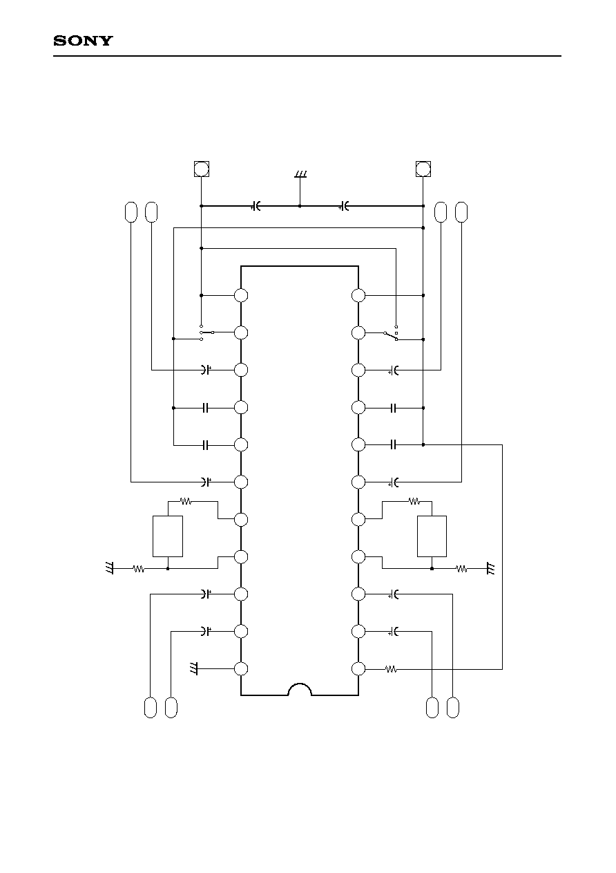
Block Diagram and Pin Configuration
Note) This figure shows SDIP package.
For SOP package, refer to the Pin
Description or Application Circuit.

≠ 3 ≠
CXA1560S, CXA1561M/S, CXA1562M/S
Pin Description and Equivalent Circuit
Pin No.
Symbol
Z: Imp
VDC (V)
Equivalent circuit
Description
SOP SDIP
1
3, 22 3, 20
5, 20 5, 18
1
IREF
0
40k
62k
0
V
EE
+ 1.25V
VCT
VCT
VCT
Reference current pin for
setting internal filter cut-off
frequency
Recording input pin
Reference level = ≠25dBm
Buffer amplifier output pin
to drive multiplex filter
Reference level = ≠15dBm
Playback input pin
Reference level = ≠30dBm
Buffer amplifier input pin to
drive multiplex filter
Reference level = ≠19dBm
2, 21 PB IN
MPX IN
LINE IN
MPX OUT
2, 23
4, 19
4, 21
V
EE
+ 1.25V
V
CC
V
EE
V
CC
V
EE
VCT
40k
V
CC
VCT
V
EE
62k
V
CC
V
EE
500
500
8.8k

≠ 4 ≠
CXA1560S, CXA1561M/S, CXA1562M/S
VDC (V)
SOP SDIP
6, 19
8, 17 8, 15
9, 16 9, 14
6, 17 LINE OUT
0
--
--
0
VCT
V
EE
+ 0.4V
V
EE
+ 0.4V
VCT
Line output pin
Time constant connecting
pin for LLS detector
Recording output pin
Reference level = ≠6dBm
Time constant connecting
pin for HLS detector
7, 16 TCH
TCL
REC OUT
7, 15
V
CC
V
EE
200
200
13k
36k
330k
V
CC
V
EE
13.5k
480k
V
CC
V
EE
V
CC
V
EE
200
200
Z: Imp
Pin No.
Symbol
Equivalent circuit
Description

≠ 5 ≠
CXA1560S, CXA1561M/S, CXA1562M/S
VDC (V)
SOP SDIP
10
24
14
10
MODE
VCT
--
--
MODE control pin
H: REC (Filter ON)
M: REC (Filter OFF)
L: PB
Dual power supply: GND
Single power supply: Vcc/2
Vcc
0
12
15
13
NRSW
V
EE
V
CC
--
--
VCT
V
EE
V
CC
V
EE
50µA
22k
50k
V
CC
V
EE
50µA
22k
50k
11
11
V
CC
22
NR control pin
H: C type
M: B type
L: NR OFF
Dual power supply: V
EE
Single power supply:
GND pin
Z: Imp
Pin No.
Symbol
Equivalent circuit
Description

≠ 6 ≠
CXA1560S, CXA1561M/S, CXA1562M/S
Electrical Characteristics
Ta = 25∞C, Dolby level: ≠6dBm (= 388mVrms) at REC OUT,
V
CC
= 15V (CXA1560), V
CC
= 12V (CXA1561), V
CC
= 9V (CXA1562)
Characteristics
Operating voltage
CXA1560
CXA1561
CXA1562
Current consumption
CXA1560
CXA1561
CXA1562
LINE OUT level
CXA1560
CXA1561
CXA1562
LINE IN level
PB IN level
MPX amplifier gain
Encode characteristics
B type boost
(1)
(2)
(3)
(4)
C type boost
(1)
(2)
(3)
(4)
(5)
(6)
Symbol
R/P
NR
f (Hz) Other conditions
Min.
Typ.
Max.
Unit
Vopr
I
CC
Vlout
Vlin
Vpin
Gmpx
B-R-1
B-R-2
B-R-3
B-R-4
C-R-1
C-R-2
C-R-3
C-R-4
C-R-5
C-R-6
--
REC
REC
REC
PB
MPX
REC
REC
REC
REC
REC
REC
REC
REC
REC
REC
--
OFF
OFF
OFF
OFF
OFF
B
B
B
B
C
C
C
C
C
C
--
--
1k
1k
1k
1k
500
5k
10k
10k
500
500
2k
2k
5k
10k
No Signal
≠25dB
≠25dB
≠40dB
0dB
≠60dB
≠25dB
≠60dB
≠25dB
≠25dB
0dB
11.5
8.5
7.2
8.0
8.0
8.0
≠1.0
≠4.0
≠7.0
≠27
≠32
9.0
1.4
3.9
9.7
≠1.1
14.2
7.2
18.7
5.4
3.5
≠5.5
--
--
--
13.2
13.0
12.8
0.0
≠3.0
≠6.0
≠25
≠30
10.0
2.9
5.4
10.4
0.4
16.2
9.2
20.7
7.4
5.5
≠3.5
16.0
16.0
16.0
18.0
18.0
18.0
1.0
≠2.0
≠5.0
≠23
≠28
11.0
4.4
6.9
11.4
1.9
18.2
11.2
22.7
9.4
7.5
≠1.5
V
V
V
mA
mA
mA
dBm
dBm
dBm
dBm
dBm
dB
dB
dB
dB
dB
dB
dB
dB
dB
dB
dB
Measurement conditions

≠ 7 ≠
CXA1560S, CXA1561M/S, CXA1562M/S
Signal handling
CXA1560
CXA1561
CXA1562
Total harmonic distortion
1) NR OFF
CXA1560
CXA1561
CXA1562
2) B
CXA1560
CXA1561
CXA1562
3) C
CXA1560
CXA1561
CXA1562
S/N
REC-PB
PB-REC
REC ch to ch
REC OUT offest
Voltage
(OFF-C type)
Vomax
THD
(OFF)
THD
(B)
THD
(C)
SN
(CCIR)
CT-1
CT-2
CT-3
Voff
REC
REC
REC
REC
REC
PB
REC
REC
REC
OFF
OFF
B
C
C
OFF
OFF
OFF
OFF
C
1k
1k
1k
1k
--
1k
1k
1k
--
THD = 1%
+10dB
+10dB
+10dB
Rg = 5
(CCIR/ARM)
0dB
0dB
0dB
13.5
13.5
13.5
--
--
--
--
--
--
--
--
--
60
--
--
--
≠100
16.0
16.2
16.0
0.03
0.02
0.02
0.03
0.03
0.04
0.04
0.04
0.05
64
≠80
≠87
≠73
0
--
--
--
0.1
0.1
0.1
0.1
0.1
0.1
0.2
0.2
0.2
--
≠70
≠70
≠65
100
dB
dB
dB
%
%
%
%
%
%
%
%
%
dB
dB
dB
dB
mV
0dB means the level which provides the Dolby level to recording output when NR is off.
Characteristics
Symbol
R/P
NR
f (Hz) Other conditions
Min.
Typ.
Max.
Unit
Measurement conditions

≠ 8 ≠
CXA1560S, CXA1561M/S, CXA1562M/S
RECOUT1
MODE
V
CC
LINEOUT1
TCH1
TCL1
MPXIN1
MPXOUT1
VCT
PBIN1
LINEIN1
NRSW
GND
TCL2
RECOUT2
LINEOUT2
TCH2
MPXIN2
MPXOUT2
LINEIN2
IREF
PBIN2
C1
100µ
S21
VNRSW
CXA1560S/A1561S/A1562S
A
DC Volt
Meter
C25
68n
C24
100n
C23
1µ
R21
3.3k
R22
6.8k
C21
1µ
R1
20k
C22
1µ
CCIR/ARM
Filter
Audio
Analyzer
C26
1µ
Audio
SG
S22
S1
-2
S2
-2
S3
S12
S11
2
3
4
5
6
7
8
9
10
11
1
V
CC
S2
-1
S1
-1
VMODE
C16
1µ
C15
68n
C14
100n
C13
1µ
R11
3.3k
R12
6.8k
C12
1µ
C11
1µ
C2
100µ
12
13
14
15
16
17
18
19
20
21
22
Electrical Characteristics Measurement Circuit
≠ 9 ≠
CXA1560S, CXA1561M/S, CXA1562M/S
RECOUT1
MODE
V
CC
LINEOUT1
TCH1
TCL1
MPXIN1
MPXOUT1
VCT
PBIN1
LINEIN1
NRSW
V
EE
TCL2
RECOUT2
LINEOUT2
TCH2
MPXIN2
MPXOUT2
LINEIN2
IREF
PBIN2
C2
10µ
CXA1560S/1561S/1562S
C23
1µ
R21
3.3k
(5%)
C21
1µ
R1
20k
(2%)
C22
1µ
C12
1µ
C11
1µ
R22
6.8k
(5%)
MPX
Filter
C24
100n
(10%)
C25
68n
(10%)
C26
1µ
P1
V
EE
P23
P24
RECOUT2
LINEOUT2
OFF
B
C
P21
P22
PBIN2
LINEIN2
P12
P11
LINEIN1
PBIN1
R12
6.8k
(5%)
MPX
Filter
R11
3.3k
(5%)
2
3
4
5
6
7
8
9
10
11
1
C13
1µ
C14
100n
(10%)
MPX
OFF
PB
MPX
ON
P2
V
CC
C15
68n
(10%)
C16
1µ
P14
P13
LINEOUT1
RECOUT1
C1
10µ
12
13
14
15
16
17
18
19
20
21
22
Application Circuit
Switchable Processor with Dual Power Supply (CXA1560S/1561S/1562S)
Application circuits shown are typical examples illustrating the operation of the devices. Sony cannot assume responsibility fo
r
any problems arising out of the use of these circuits or for any infringement of third party patent and other right due to same
.
Note) Resistor and capacitor tolerances are ±
10% and ±
20% respectively, unless otherwise specified.
≠ 10 ≠
CXA1560S, CXA1561M/S, CXA1562M/S
C2
10µ
C23
1µ
R21
3.3k
(5%)
C21
1µ
R1
20k
(2%)
C22
1µ
C12
1µ
C11
1µ
R22
6.8k
(5%)
MPX
Filter
C24
100n
(10%)
C25
68n
(10%)
C26
1µ
P1
V
EE
P23
P24
RECOUT2
LINEOUT2
OFF
B
C
P21
P22
PBIN2
LINEIN2
P12
P11
LINEIN1
PBIN1
R12
6.8k
(5%)
MPX
Filter
R11
3.3k
(5%)
C13
1µ
C14
100n
(10%)
MPX
OFF
PB
MPX
ON
P2
V
CC
C15
68n
(10%)
C16
1µ
P14
P13
LINEOUT1
RECOUT1
C1
10µ
RECOUT1
MODE
V
CC
LINEOUT1
TCH1
TCL1
MPXIN1
MPXOUT1
VCT
PBIN1
LINEIN1
NRSW
V
EE
TCL2
RECOUT2
LINEOUT2
TCH2
MPXIN2
MPXOUT2
LINEIN2
IREF
PBIN2
CXA1561M/1562M
2
3
4
5
6
7
8
9
10
11
1
12
13
14
15
16
17
18
19
20
21
22
23
24
N.C.
N.C.
Switchable Processor with Dual Power Supply (CXA1561M/1562M)
Application circuits shown are typical examples illustrating the operation of the devices. Sony cannot assume responsibility fo
r
any problems arising out of the use of these circuits or for any infringement of third party patent and other right due to same
.
Note) Resistor and capacitor tolerances are ±
10% and ±
20% respectively, unless otherwise specified.

≠ 11 ≠
CXA1560S, CXA1561M/S, CXA1562M/S
RECOUT1
MODE
V
CC
LINEOUT1
TCH1
TCL1
MPXIN1
MPXOUT1
VCT
PBIN1
LINEIN1
NRSW
V
EE
TCL2
RECOUT2
LINEOUT2
TCH2
MPXIN2
MPXOUT2
LINEIN2
IREF
PBIN2
C2
47µ
CXA1560S/1561S/1562S
C23
1µ
R21
3.3k
(5%)
C21
1µ
R1
20k
(2%)
C22
1µ
C12
1µ
C11
1µ
R22
6.8k
(5%)
MPX
Filter
C24
100n
(10%)
C25
68n
(10%)
C26
1µ
P1
GND
P23
P24
RECOUT2
LINEOUT2
OFF
B
C
P21
P22
PBIN2
LINEIN2
P12
P11
LINEIN1
PBIN1
R12
6.8k
(5%)
MPX
Filter
R11
3.3k
(5%)
C13
1µ
C14
100n
(10%)
MPX
OFF
PB
MPX
ON
P2
V
CC
C15
68n
(10%)
C16
1µ
P14
P13
LINEOUT1
RECOUT1
C1
10µ
12
13
14
15
16
17
18
19
20
21
22
2
3
4
5
6
7
8
9
10
11
1
Switchable Processor with Single Power Supply (CXA1560S/1561S/1562S)
Application circuits shown are typical examples illustrating the operation of the devices. Sony cannot assume responsibility fo
r
any problems arising out of the use of these circuits or for any infringement of third party patent and other right due to same
.
Note) Resistor and capacitor tolerances are ±
10% and ±
20% respectively, unless otherwise specified.

≠ 12 ≠
CXA1560S, CXA1561M/S, CXA1562M/S
RECOUT1
MODE
V
CC
LINEOUT1
TCH1
TCL1
MPXIN1
MPXOUT1
VCT
PBIN1
LINEIN1
NRSW
V
EE
TCL2
RECOUT2
LINEOUT2
TCH2
MPXIN2
MPXOUT2
LINEIN2
IREF
PBIN2
C2
47µ
CXA1561M/1562M
C23
1µ
R21
3.3k
(5%)
C21
1µ
R1
20k
(2%)
C22
1µ
C12
1µ
C11
1µ
R22
6.8k
(5%)
MPX
Filter
C24
100n
(10%)
C25
68n
(10%)
C26
1µ
P1
GND
P23
P24
RECOUT2
LINEOUT2
OFF
B
C
P21
P22
PBIN2
LINEIN2
P12
P11
LINEIN1
PBIN1
R12
6.8k
(5%)
R11
3.3k
(5%)
C13
1µ
C14
100n
(10%)
MPX
OFF
PB
MPX
ON
P2
V
CC
C15
68n
(10%)
C16
1µ
P14
P13
LINEOUT1
RECOUT1
C1
10µ
N.C.
N.C.
12
2
3
4
5
6
7
8
9
10
11
1
13
14
15
16
17
18
19
20
21
22
23
24
MPX
Filter
Switchable Processor with Single Power Supply (CXA1561M/1562M)
Application circuits shown are typical examples illustrating the operation of the devices. Sony cannot assume responsibility fo
r
any problems arising out of the use of these circuits or for any infringement of third party patent and other right due to same
.
Note) Resistor and capacitor tolerances are ±
10% and ±
20% respectively, unless otherwise specified.

≠ 13 ≠
CXA1560S, CXA1561M/S, CXA1562M/S
Application Note
The CXA1560 series is a stereo Dolby B-C type NR IC like the CXA1330 series.
Built-in spectral skewing circuit allows smaller package.
1) Power Supply
The CXA1560 series is designed to operate on either single or dual power supply.
For dual power supply, connect VCT to GND, and V
EE
to the negative power supply.
For single power supply, connect V
EE
to GND. Vcc/2, generated from the internal circuit, is output to VCT.
Connect a by-pass capacitor between this pin and GND.
The operating voltage range is ±3.5 to ±8.0V (7.0 to 16V), which satisfies the signal handling of 12dB
specified by the Dolby Laboratories.
2) Operation Mode Control
The CXA1560 series has built-in electronic switches. The operations are controlled by the DC voltages of
NRSW and MODE control pins. Table 1 shows the switching truth tables.
For single power supply, VH, VM, and VL correspond to Vcc, Vcc/2 and GND, respectively.
For dual power supply, VH, VM and VL correspond to Vcc, GND and V
EE
, respectively.
Refer to "threshold" on the characteristics graph for the thresholds of the control voltages. NRSW and
MODE control pins are connected to VCT via a 50k
resistor, so when the pin is open, VM condition
results.
Table 1
VH
VM
VL
NRSW
MODE
C type
MPX ON
REC
(Encode)
B type
MPX OFF
REC
(Encode)
NR OFF
PB
(Decode)
3) Reference level
The CXA1560 series Dolby level is ≠6dBm (388mVrms), and is measured at the recording output pin (REC
OUT) in the NR OFF mode. The reference level of the recording input pin (LINE IN), playback input pin (PB
IN) and line output pin (LINE OUT) are defined as the levels which provide Dolby level at the recording
output pin in NR OFF mode.
4) MPX Filter
The CXA1560 series provides an MPX (FM multiplex) filter ON/OFF function.
Connect the MPX filter between MPX IN and MPX OUT. In MPX ON mode, the line input signal is fed to the
NR processor via the MPX buffer amplifier and MPX filter. In MPX OFF mode, the signal bypasses the
buffer amplifier and filter, and is fed directly to the NR processor. The MPX buffer amplifier gain is 10dB.
The gain from LINE IN to LINE OUT is 19dB, and from MPX IN to LINE OUT it is 13dB, for a deviation of
6dB. This means that if a filter with insertion loss of 4dB is used, there is no fluctuation between MPX ON
and MPX OFF.
≠ 14 ≠
CXA1560S, CXA1561M/S, CXA1562M/S
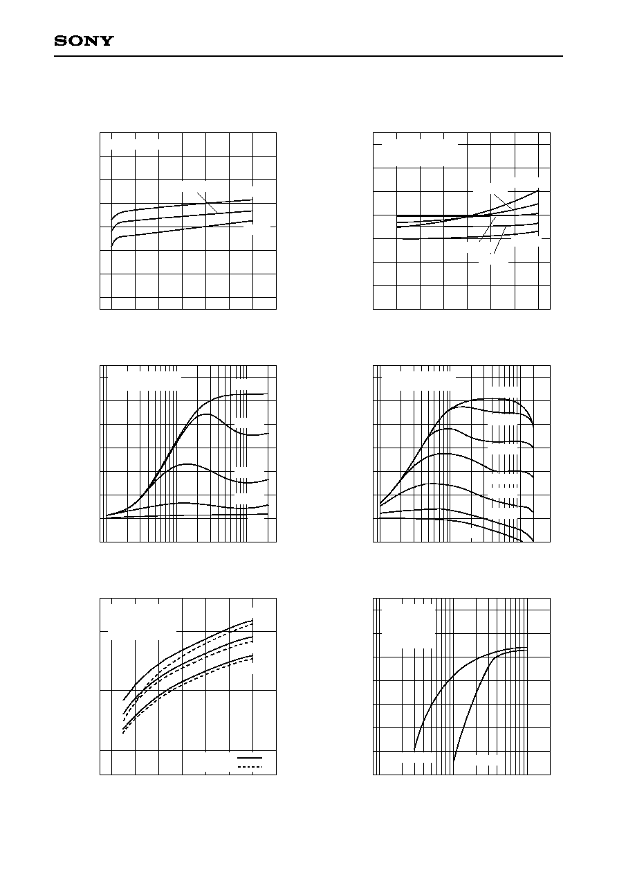
Example of Representative Characteristics
Quiescent current consumption vs. Supply voltage
16
V
CC
-V
EE
≠ Supply voltage [V]
4
6
8
10
12
14
8
10
11
12
13
14
15
I
CC
≠
Quiescent current consumptionl [mA]
Encode Mode
B type
NR OFF
C type
Current consumption vs. Input level
12
Input level [dB]
≠12
≠8
≠4
0
4
8
10
11
12
13
14
15
16
I
CC
≠
Current consumption [mA]
Encode Mode
V
CC
= ±6V
0dB = Dolby Level
Cf = 10k
Cf = 1k
Bf = 10k
NR OFF
Bf = 1k
C type encode characteristics
10k
Frequency [Hz]
100 200
500
1k
2k
5k
0
4
8
12
16
20
24
Encode boost [dB]
V
CC
= ±6V
0dB = Dolby Level
20k
≠60dB
≠50dB
≠40dB
≠30dB
≠20dB
≠10dB
0dB
B type encode characteristics
10k
Frequency [Hz]
100 200
500
1k
2k
5k
0
2
4
6
8
10
12
Encode boost [dB]
V
CC
= ±6V
0dB = Dolby Level
20k
≠40dB
≠30dB
≠20dB
≠10dB
0dB
Load characteristics
Load resistance [
]
200
500
1k
2k
5k
10k
4
6
8
10
12
14
16
Maximum output level [dBm]
Encode Mode
V
CC
= ±6V
THD = 1%
f = 1kHz
NR OFF
LINE OUT
REC OUT
Signal handling
V
CC
-V
EE
≠ Supply voltage [V]
4
8
10
12
14
16
0
Signal handling [dB]
Encode Mode
f = 1kHz
THD = 1%
0dB = Dolby Level
10
20
6
A1562
A1561
A1560
NR OFF
C type

≠ 15 ≠
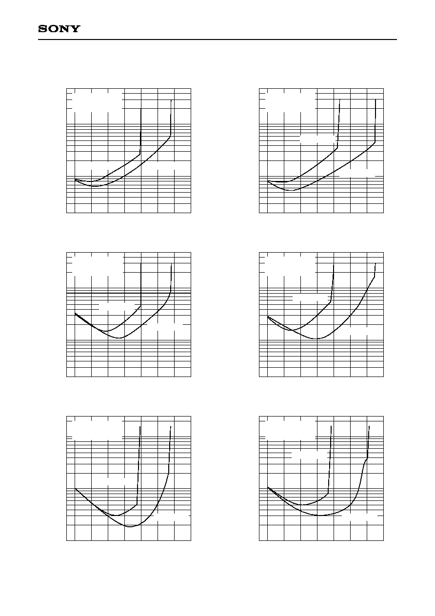
CXA1560S, CXA1561M/S, CXA1562M/S
NR OFF total harmonic distortion-1 (CXA1561)
Output level [dB]
≠4
0.1
Distortion [%]
Encode Mode
V
CC
= ±6.0V
0dB = Dolby Level
0.01
0
4
8
12
16
20
f = 100Hz
f = 1kHz
f = 10kHz
NR OFF total harmonic distortion-2 (CXA1560)
Output level [dB]
≠4
0.1
Distortion [%]
Encode Mode
f = 1kHz
0dB = Dolby Level
0.01
0
4
8
12
16
20
V
CC
= ±5.5V
V
CC
= ±8.0V
B type total harmonic distortion-2 (CXA1560)
Output level [dB]
≠4
0.1
Distortion [%]
Encode Mode
f = 1kHz
0dB = Dolby Level
0.01
0
4
8
12
16
20
V
CC
= ±5.5V
V
CC
= ±8.0V
B type total harmonic distortion-1 (CXA1561)
Output level [dB]
≠4
0.1
Distortion [%]
Encode Mode
V
CC
= ±6.0V
0dB = Dolby Level
0.01
0
4
8
12
16
20
f = 100Hz
f = 1kHz
f = 10kHz
C type total harmonic distortion-1 (CXA1561)
Output level [dB]
≠4
1.0
Distortion [%]
Encode Mode
V
CC
= ±6.0V
0dB = Dolby Level
0.1
0
4
8
12
16
20
0.01
f = 100Hz
f = 1kHz
f = 10kHz
C type total harmonic distortion-2 (CXA1560)
Output level [dB]
≠4
1.0
Distortion [%]
Encode Mode
f = 1kHz
0dB = Dolby Level
0.1
0
4
8
12
16
20
0.01
V
CC
= ±5.5V
V
CC
= ±8.0V
≠ 16 ≠
CXA1560S, CXA1561M/S, CXA1562M/S
NR OFF total harmonic distortion-4 (CXA1562)
Output level [dB]
≠4
0.1
Distortion [%]
Encode Mode
f = 1kHz
0dB = Dolby Level
0.01
0
4
8
12
16
20
V
CC
= ±3.5V
V
CC
= ±8.0V
NR OFF total harmonic distortion-3 (CXA1561)
Output level [dB]
≠4
0.1
Distortion [%]
Encode Mode
f = 1kHz
0dB = Dolby Level
0.01
0
4
8
12
16
20
V
CC
= ±4.0V
V
CC
= ±8.0V
B type total harmonic distortion-3 (CXA1561)
Output level [dB]
≠4
0.1
Distortion [%]
Encode Mode
f = 1kHz
0dB = Dolby Level
0.01
0
4
8
12
16
20
V
CC
= ±4.0V
V
CC
= ±8.0V
C type total harmonic distortion-3 (CXA1561)
Output level [dB]
≠4
1.0
Distortion [%]
Encode Mode
f = 1kHz
0dB = Dolby Level
0.1
0
4
8
12
16
20
0.01
V
CC
= ±4.0V
V
CC
= ±8.0V
C type total harmonic distortion-4 (CXA1562)
Output level [dB]
≠4
1.0
Distortion [%]
Encode Mode
f = 1kHz
0dB = Dolby Level
0.01
0
4
8
12
16
20
V
CC
= ±3.5V
V
CC
= ±8.0V
B type total harmonic distortion-4 (CXA1562)
Output level [dB]
≠4
0.1
Distortion [%]
Encode Mode
f = 1kHz
0dB = Dolby Level
0.01
0
4
8
12
16
20
V
CC
= ±3.5V
V
CC
= ±8.0V

≠ 17 ≠
CXA1560S, CXA1561M/S, CXA1562M/S
Cross talk
Frequency [Hz]
100
≠40
Cross talk [dB]
V
CC
= ±6V
Input = +10dB
Refer to Dolby Level
NR OFF
REC ch to ch
≠100
≠50
≠60
≠70
≠80
≠90
200
500
1k
2k
5k
10k
PB to REC
REC to PB
PB ch to ch
NR control threshold
V
CC
≠ Supply voltage [V]
4
14
V
CN
≠
NR control voltage [V]
2
12
10
8
6
4
6
8
10
12
14
16
0
NR OFF
B type
C type
V
CC
V
CC
2
MODE control threshold
V
CC
≠ Supply voltage [V]
4
14
V
CM
≠
MODE control voltage [V]
2
12
10
8
6
4
6
8
10
12
14
16
0
PB
MPX OFF
MPX ON
V
CC
V
CC
2

≠ 18 ≠
CXA1560S, CXA1561M/S, CXA1562M/S
CXA1560S, CXA1561S, CXA1562S
SONY CODE
EIAJ CODE
JEDEC CODE
M
PACKAGE STRUCTURE
MOLDING COMPOUND
LEAD TREATMENT
LEAD MATERIAL
PACKAGE MASS
EPOXY RESIN
SOLDER PLATING
42/COPPER ALLOY
24PIN SOP (PLASTIC)
15.0 ≠ 0.1
+ 0.4
1
12
13
24
0.45
±
0.1
5.3
≠
0.1
+ 0.3
7.9
±
0.4
0.2 ≠ 0.05
+ 0.1
0.5
±
0.2
0.1 ≠ 0.05
+ 0.2
0.15
1.85 ≠ 0.15
+ 0.4
6.9
0.24
SOP-24P-L01
SOP024-P-0300
0.3g
1.27
SONY CODE
EIAJ CODE
JEDEC CODE
PACKAGE STRUCTURE
MOLDING COMPOUND
LEAD TREATMENT
LEAD MATERIAL
PACKAGE MASS
EPOXY RESIN
SOLDER PLATING
COPPER ALLOY
22PIN SDIP (PLASTIC)
SDIP-22P-01
SDIP022-P-0300
0.95g
1.778
11
12
1
22
19.2 ≠ 0.1
+ 0.4
7.62
6.4
≠
0.1
+ 0.3
0.25
≠
0.05
+ 0.1
0∞ to 15∞
0.5
±
0.1
0.9 ≠ 0.1
+ 0.15
3.25
≠
0.2
+ 0.15
0.51 MIN
3.9
≠
0.1
+ 0.4
1.All mat surface type.
Two kinds of package surface:
2.All mirror surface type.
Package Outline
Unit: mm
CXA1561M, CXA1562M

≠ 19 ≠
CXA1560S, CXA1561M/S, CXA1562M/S
Package Outline
Unit: mm
CXA1562S
PEC Ass'y
SONY CODE
EIAJ CODE
JEDEC CODE
PACKAGE STRUCTURE
MOLDING COMPOUND
LEAD TREATMENT
LEAD MATERIAL
PACKAGE MASS
EPOXY RESIN
SOLDER PLATING
COPPER ALLOY
22PIN SDIP (PLASTIC)
SDIP-22P-01
SDIP022-P-0300
0.95g
1.778
11
12
1
22
19.2 ≠ 0.1
+ 0.4
7.62
6.4
≠
0.1
+ 0.3
0.25
≠
0.05
+ 0.1
0∞ to 15∞
0.5
±
0.1
0.9 ≠ 0.1
+ 0.15
3.25
≠
0.2
+ 0.15
0.51 MIN
3.9
≠
0.1
+ 0.4
1.All mat surface type.
Two kinds of package surface:
2.All mirror surface type.
LEAD PLATING SPECIFICATIONS
ITEM
LEAD MATERIAL
COPPER ALLOY
SOLDER COMPOSITION
Sn-Bi Bi:1-4wt%
PLATING THICKNESS
5-18
µ
m
SPEC.
Sony Corporation