--1--
E93503-TE
Sony reserves the right to change products and specifications without prior notice. This information does not convey any license by
any implication or otherwise under any patents or other right. Application circuits shown, if any, are typical examples illustrating the
operation of the devices. Sony cannot assume responsibility for any problems arising out of the use of these circuits.
Absolute Maximum Ratings
(Ta=25∞C)
∑ Supply voltage
Vcc
12
V
∑ Operating temperature
Topr
≠40 to +85
∞C
∑ Storage temperature
Tstg
≠65 to +150
∞C
∑ Allowable power dissipation
P
D
430
mW
Recommended Operating Condition
Supply voltage
Vcc
6.5 to 11
V
Description
The CXA1580Q is an IC designed for use in car
stereos. Functions include Dolby B type noise
reduction, playback equalizer and interval detection
between tracks (MUSIC SENSOR) into a single
chip.
Features
∑ Few external parts
∑ Forward/Reverse head switching
∑ 3-input selector switch (TAPE, CD, RADIO)
∑ Small package (40-pin QFP)
∑ Dolby B type noise reduction and playback
equalizer into a single chip
∑ Same pin configuration as Dolby B/C type noise
reduction system (CXA1581)
∑ Interval detection level between tracks can be set
by external resistors/capacitors (2 modes).
Applications
∑ Car stereos
∑ Stereo cassette deck players (playback only)
Structure
Bipolar silicon monolithic IC
Dolby B Type Noise Reduction System with Playback Equalizer
40 pin QFP (Plastic)
CXA1580Q
* "Dolby" and the double D symbols are trademarks of Dolby Laboratories Licensing Corporation.
For the availability of this product, please contact the sales office.

--3--
CXD1580Q
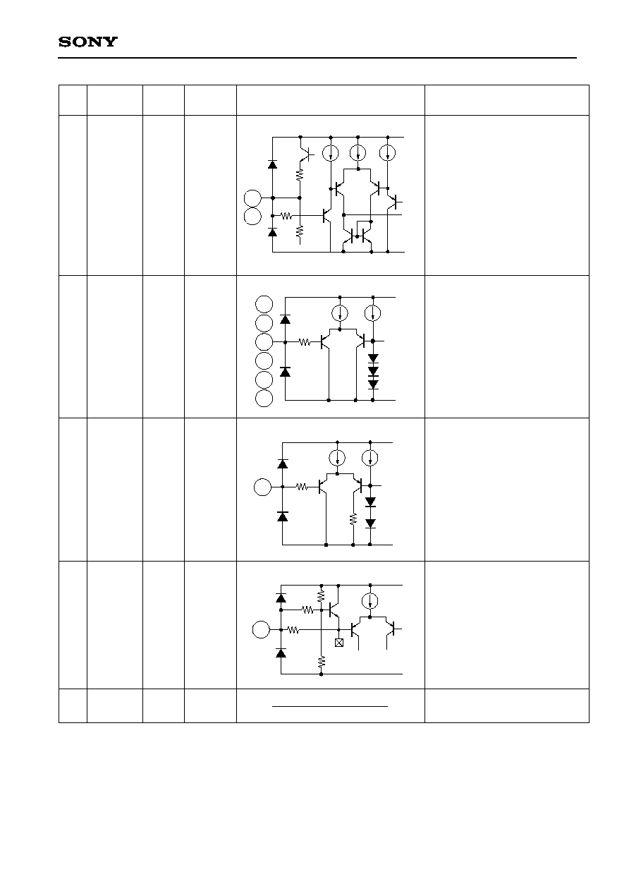
Pin Description
(Ta=25∞C, Vcc=8.0V, no signal)
Pin
Symbol
DC
I/O
Equivalent circuit
Description
No.
value
resistance
1
PBOUT
2.8V
--
30
32
PBFB
1.4V
150k
39
33
PBIN
0V
70k
34
37
38
2
Vcc
8.0V
--
10
GND
0.0V
--
29
MSGND
35
PBGND
31
PBTC
--
--
40
36
E IREF
1.25V
--
11
MSOUT
--
PBEQ output
PBEQ feedback
PBEQ input
Power supply
Ground
PBEQ capacitance
Connection of reference current
setting resistor for PBEQ block.
MS output
147
42µ
30µ
Vcc
GND
31
40
147
10µ
1.25V
Vcc
GND
36
147
Vcc
GND
10k
V
DD
=5V
11
Refer to Page 6.
0.0V for
signal
detection;
5.0V for
no signal
detection