 | –≠–Ľ–Ķ–ļ—ā—Ä–ĺ–Ĺ–Ĺ—č–Ļ –ļ–ĺ–ľ–Ņ–ĺ–Ĺ–Ķ–Ĺ—ā: CXA1665 | –°–ļ–į—á–į—ā—Ć:  PDF PDF  ZIP ZIP |

≠ 1 ≠
CXA1665AM/AM-S
E95826A63-ST
All Band TV Tuner IC (VHF-CATV-UHF)
Description
The CXA1665AM/AM-S is a single chip TV tuner
IC which performs as an oscillator, mixer for
VHF/CATV and UHF bands. An IF amplifier is also
provided.
This IC adopts a 16-pin SOP package in response
to the trend toward miniaturizing the tuner and
automatic IC mounting. This IC achieves a large
reduction of external parts in addition to
miniaturizing the tuner and increasing manufacturing
productivity, reliability and design efficiency.
Features
∑ On-chip oscillator and mixer for UHF band
∑ Low noise figure
∑ Reduced spurious interference
∑ Superior cross modulation distortion
∑ Stable oscillating characteristics
Absolute Maximum Ratings (Ta = 25įC)
∑ Supply voltage
V
CC
11
V
∑ Storage temperature
Tstg ≠65 to +150 įC
∑ Allowable power dissipation P
D
980
mW
(When mounted on a board)
Block Diagram and Pin Configuration (Top View)
Structure
Bipolar silicon monolithic IC
Applications
∑ CTV tuner
∑ CATV UP-DOWN converter
∑ FM detector for 2nd IF satellite broadcasts
Operation Conditions
∑ Supply voltage
V
CC
9.0 Ī 0.9
V
∑ Operating temperature
Topr ≠20 to +75
įC
Sony reserves the right to change products and specifications without prior notice. This information does not convey any license by
any implication or otherwise under any patents or other right. Application circuits shown, if any, are typical examples illustrating the
operation of the devices. Sony cannot assume responsibility for any problems arising out of the use of these circuits.
16 pin SOP (Plastic)
SW
UHF OSC
UHF MIX
VHF MIX
IF
AMP
≠
+
VHF OSC
VOSC C
UOSC B2
UOSC E2
UOSC E1
UOSC B1/SW
REG
UHF IN2
UHF IN1
VOSC B
GND
MIX OUT1
MIX OUT2
IF OUT
V
CC
VHF IN1
VHF IN2
2
3
4
5
7
8
1
9
10
11
12
13
14
15
16
6
V.
REG

≠ 2 ≠
CXA1665AM/AM-S
Pin Description and Equivalent Circuit
Pin
No.
Symbol
Typical
voltage (V)
Equivalent circuit
Description
1
16
VOSC B
VOSC C
3
4
MIX OUT1
MIX OUT2
Under VHF
operating; 3.5
Under UHF
operating; 3.7
6.7
9.0
7.5
7.3
7.5
7.3
VHF ocsillator.
Mixer output and IF
amplifier input.
5
IF OUT
4.5
4.5
IF output.
2
GND
0
GND
6
V
CC
9
Power supply.
16
6
1
800
25P
3k
V
CC
3k
6
V
CC
450
5k
3
4
450
5k
5
6
V
CC
55

≠ 3 ≠
CXA1665AM/AM-S
7
8
VHF IN1
VHF IN2
3.2
3.3
3.2
3.3
VHF input; normally a
decoupling capacitor is
connected at Pin 7 to
GND and Pin 8 is used
for input.
9
10
UHF IN1
UHF IN2
3.3
3.2
3.3
3.2
UHF input.
The balanced input to
Pins 9 and 10, or a
decoupling capacitor is
connected at Pin 10 to
GND and Pin 9 is used
for input.
11
REG
6
12
UOSC
B1/SW
13
UOSC E1
14
UOSC E2
15
UOSC B2
0
0
3.2
3.7
3.4
2.6
2.6
3.4
Regulator output.
UHF oscillator.
Pin 12 is used for both
U/V switches.
3k
3k
8
7
3k
3k
10
9
11
6
V
CC
6
8k
8k
12
13
14
15
40k
V
CC
20k
Pin
No.
Symbol
Typical
voltage (V)
Equivalent circuit
Description
≠ 4 ≠
CXA1665AM/AM-S
Electrical Characteristics
(See Electrical Characteristics Measurement Circuit. Ta = 25įC, V
CC
= 9V)
1
Measured value for untuned inputs.
2
Noise figure is uncorrected for image.
3
Desired signal (f
D
) input level is ≠33dBm.
undesired signal (f
UD
) is 100kHz at 30% AM.
The measurement value is undesired signal level, it measured with a spectrum analyzer at S/I = 46dB.
4
Design guaranteed items.
Condition
VHF operation; no signal
UHF operation; no signal
VHF operation; f
RF
= 55MHz;
Input level ≠40dBm
VHF operation; f
RF
= 360MHz;
Input level ≠40dBm
UHF operation; f
RF
= 360MHz;
Input level ≠40dBm
UHF operation; f
RF
= 800MHz;
Input level ≠40dBm
VHF operation; f
RF
= 55MHz
VHF operation; f
RF
= 360MHz
UHF operation; f
RF
= 360MHz
UHF operation; f
RF
= 800MHz
VHF operation; f
D
= 55MHz, f
UD
= Ī12MHz
VHF operation; f
D
= 360MHz, f
UD
= Ī12MHz
UHF operation; f
D
= 360MHz, f
UD
= Ī12MHz
UHF operation; f
D
= 800MHz, f
UD
= Ī12MHz
50
load
VHF operation; f
OSC
= 100MHz
frequency drift for the time from 3s to
3min after switch ON
VHF operation; f
OSC
= 405MHz
frequency drift for the time from 3s to
3min after switch ON
UHF operation; f
OSC
= 405MHz
frequency drift for the time from 3s to
3min after switch ON
UHF operation; f
OSC
= 845MHz
frequency drift for the time from 3s to
3min after switch ON
VHF operation; f
OSC
= 100MHz
frequency shift when V
CC
+ 9V changes Ī5%
VHF operation; f
OSC
= 405MHz
frequency shift when V
CC
+ 9V changes Ī5%
UHF operation; f
OSC
= 405MHz
frequency shift when V
CC
+ 9V changes Ī5%
UHF operation; f
OSC
= 845MHz
frequency shift when V
CC
+ 9V changes Ī5%
Min.
30
29
20
20
25
25
96
94
88
87
+8
Typ.
45
44
23
23
28
28
10
10
7
8
100
98
92
91
+11
Max.
58
57
26
26
31
31
13
13
11
12
Ī300
Ī500
Ī500
Ī500
Ī200
Ī250
Ī250
Ī250
Unit
mA
mA
dB
dB
dB
dB
dB
dB
dB
dB
dBĶ
dBĶ
dBĶ
dBĶ
dBm
kHz
kHz
kHz
kHz
kHz
kHz
kHz
kHz
Item
Circuit current
Conversion
gain
1
Noise
figure
1
2
4
1% cross
modulation
1
3
Max. output
power
Switch ON
drift
4
+B supply
voltage drift
Symbol
I
CC
V
I
CC
U
CG1
CG2
CG3
CG4
NF1
NF2
NF3
NF4
CM1
CM2
CM3
CM4
Pomax
(sat)
fsw1
fsw2
fsw3
fsw4
fst1
fst2
fst3
fst4

≠ 5 ≠
CXA1665AM/AM-S
Electrical Characteristics Measurement Circuit
VOSC C
UOSC B2
UOSC E2
UOSC E1
UOSC B1/SW
REG
UHF IN2
UHF IN1
VOSC B
GND
MIX OUT1
MIX OUT2
IF OUT
V
CC
VHF IN1
VHF IN2
2
3
4
5
6
7
8
1
9
10
11
12
13
14
15
16
4.7n
VC
51k
L2
51k
68p
(RH)
0.5p
(UK)
1T363
1p
(UK)
1p
1n
L1
51
1n
3k
51k
1n
51
VH
VL
SW1
+9V
1T362
51k
16p
68p
68p
10T
3p
1n
1n
IF out
+9V
1n
1n
VHF in
UHF in
1n
1n
1n
10k
20k
SW2
ON:UHF
OFF:VHF
1n
0.5p
(UK)
1T363
1T363
51k
L3
0.5p
(UK)
51k
3P
2P
3P
27p
(RH)
51k
9p
(SL)
27p
(RH)
Table 1. Inductance constant
Wire
diameter
0.5
0.5
0.5
L1
L2
L3
+9V
Coil
diameter
3.2
3.2
3.8
Number
of windings
5.5T
2.5T
1.5T

≠ 6 ≠
CXA1665AM/AM-S
Description of Operation (See Electrical Characteristics Test Circuit.)
(1) VHF oscillator circuit
The differential oscillator circuit with an output at Pin 16 and an input at Pin 1.
Connect an LC resonance circuit comprising a varicap diode to Pin 16 through a coupling capacitor. The
positive feedback from the resonance circuit is applied to Pin 1 through a feedback capacitor to execute
oscillation. Note that if a parasitic capacitance across Pins 1 and 16 is too large, it may cause undesired
oscillation.
(2) VHF mixer circuit
This is a double-balanced mixer having small leakage of local oscillation signal. The RF signal is input to Pins
7 and 8. In normal use, the signal is input to one pin while the other pin is connected to GND by decoupling
capacitor. The RF signal is converted to IF with the signal supplied from oscillator. The converted RF is sent to
the IF amplifier and output to Pins 3 and 4 simultaneously.
(3) UHF oscillator circuit
UHF oscillator is formed from two collector-grounded Colpitts oscillator, and oscillation is provided at the
differential input through an LC resonator circuit including a varicap diode.
The Pin 12 also functions as UHF/VHF switch pin.
(4) UHF mixer circuit
This is the double-balanced mixer like the VHF mixer. The RF signal is input to Pins 9 and 10. There is a
balanced differential input from pre-stage double tune circuit, or an unbalanced input to Pin 9 with the capacitor
connected at Pin 10 to GND. Balanced input achieves better NF rather than unbalanced input.
Otherwise, the conditions and usage are the same as those for the VHF mixer circuit.
(5) IF amplifier circuit
The mixer output signal is amplified by the IF amplifier and output to Pin 5. The output impedance is about
75
.
(6) UHF/VHF switch circuit
UHF/VHF mode is selected by the DC voltage at Pin 12. UHF operation is chosen by inputting 9V through a
20k
resistor, and VHF operation by inputting 0V. If the UHF switch voltage is 12V not 9V, adjust the
resistance to approximately 30k
so that the DC voltage becomes almost equal between Pins 12 and 15. Be
sure to connect a resistor for discharging (approx. 10k
) if OPEN not 0V is chosen for the VHF switch voltage.
Note on Usage
Care should be taken such as grounding in placing external parts because high frequencies are present.
Adjust accordingly to prevent heat problems with special care such as the GND pattern for heat dissipation at
the portion for IC mount where heat dissipations accumulate.

≠ 7 ≠
CXA1665AM/AM-S
Example of Representative Characteristics
Conversion gain vs. Reception frequency (Untuned input)
CG -- Conversion gain [dB]
40
30
Reception frequency [MHz]
100
VHF
UHF
f
IF
= 45MH
Z
20
10
0
0
200 300 400 500 600 700 800 900
Noise figure vs. Reception frequency
(Untuned input, in DSB)
NF -- Noise figure [dB]
20
15
Reception frequency [MHz]
100
VHF
UHF
f
IF
= 45MH
Z
10
5
0
0
200 300 400 500 600 700 800 900
Circuit current vs. Supply voltage
I
CC
-- Circuit current [mA]
50
40
30
V
CC
-- Supply voltage [V]
8
9
10
VHF
UHF
I/O characteristics (Untuned input)
IF output level [dBm]
20
RF input level [dBm]
≠10
0
+10
≠20
≠30
≠40
≠50
≠50
≠40
≠30
≠20
≠10
0
10
f
IF
= 45MH
Z
f
RF
= 100MH
Z
(VHF)
CM -- Cross modulation [dBĶ
]
120
Reception frequency [MHz]
100
80
40
0
0
200 300 400 500 600 700 800 900
f
UD
= f
D
+ 12MH
Z
f
UD
= f
D
≠ 12MH
Z
100
20
60
Next adjacent cross modulation vs. Reception frequency
(Untuned input)
f
IF
= 45MHz
Interference signal: 100kHz 30% AM
≠ 8 ≠
CXA1665AM/AM-S
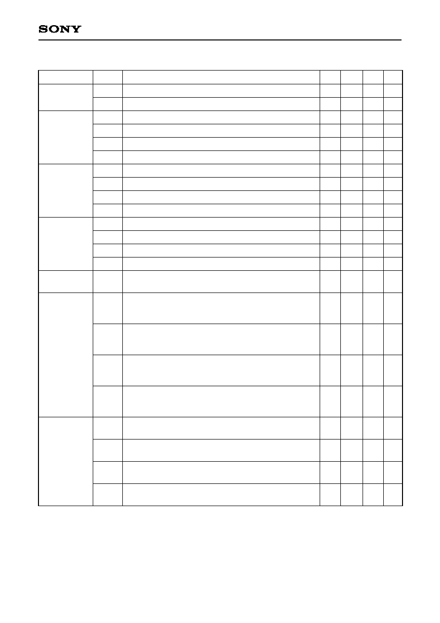
VHF Input Impedance
j50
j100
j150
j250
≠j50
≠j100
≠j150
≠j250
≠j25
≠j10
0
j25
j10
50
50MHz
100MHz
200MHz
400MHz
4
5
6
7
8
1n
S11
VHF IN1 VHF IN2
IC
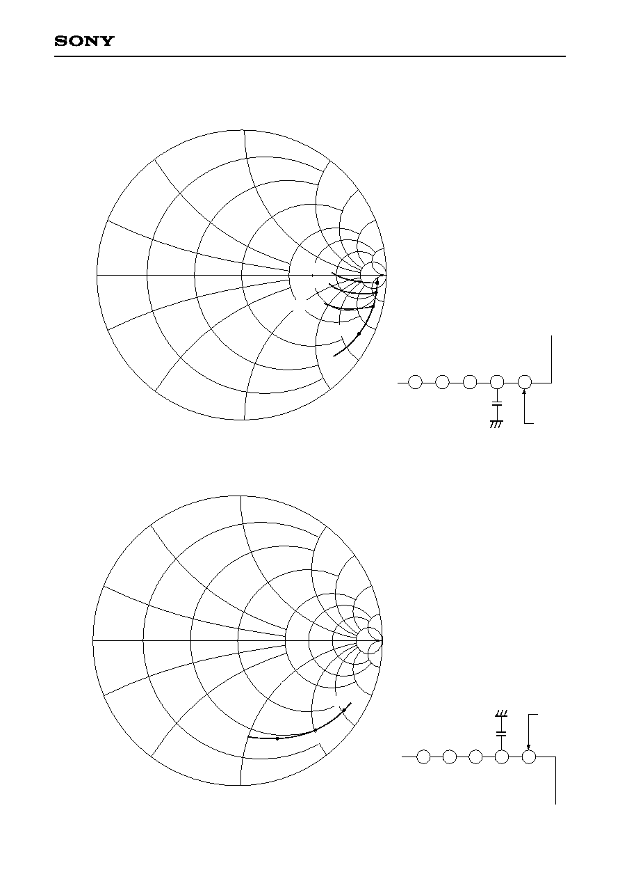
UHF Input Impedance
j50
j100
j150
j250
≠j50
≠j100
≠j150
≠j250
≠j25
≠j10
0
j25
j10
50
600MHz
800MHz
400MHz
1n
S11
UHF IN2 UHF IN1
IC
9
10
11
12
13
≠ 9 ≠
CXA1665AM/AM-S
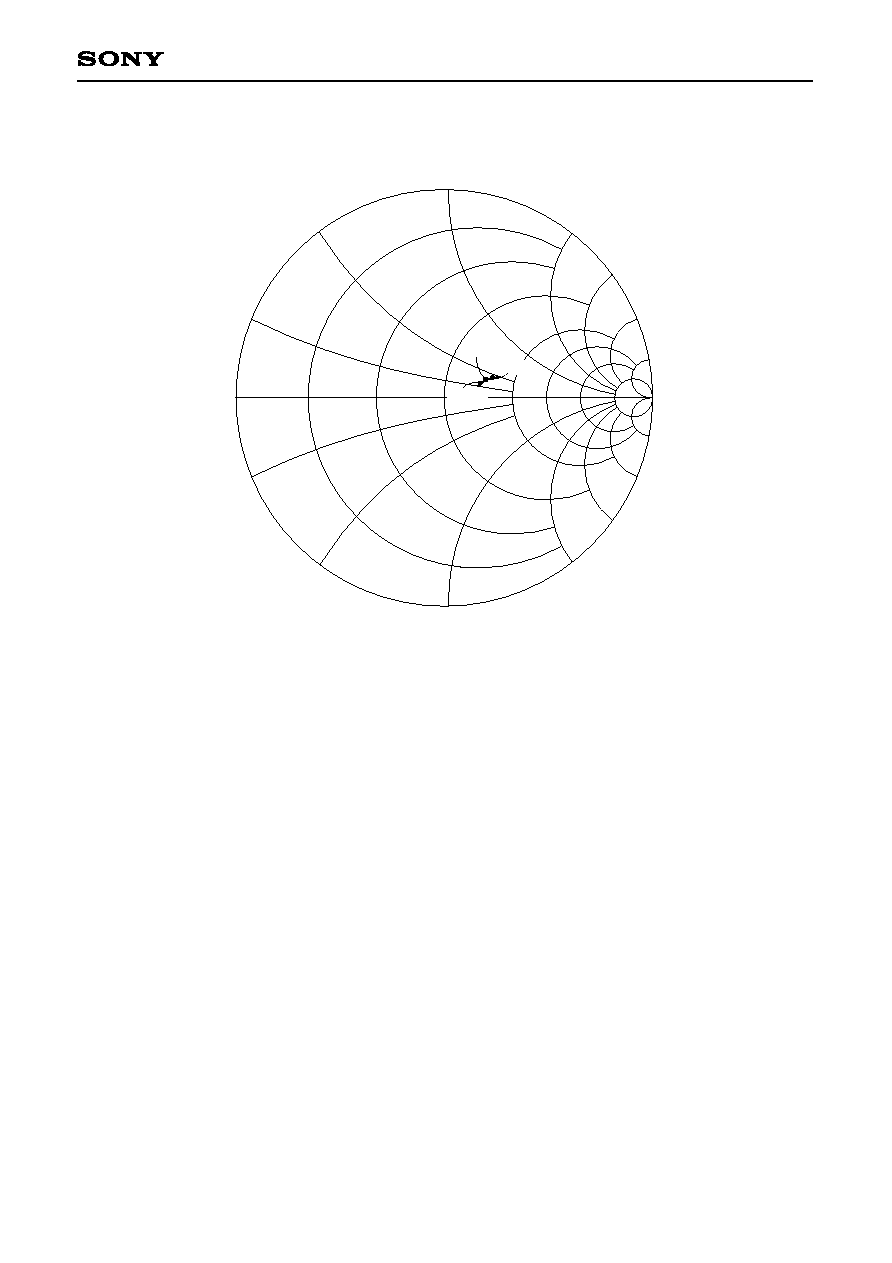
IF Output Impedance
j50
j100
j150
j250
≠j50
≠j100
≠j150
≠j250
≠j25
≠j10
0
j25
j10
50
40MHz
50MHz
60MHz
≠ 10 ≠
CXA1665AM/AM-S
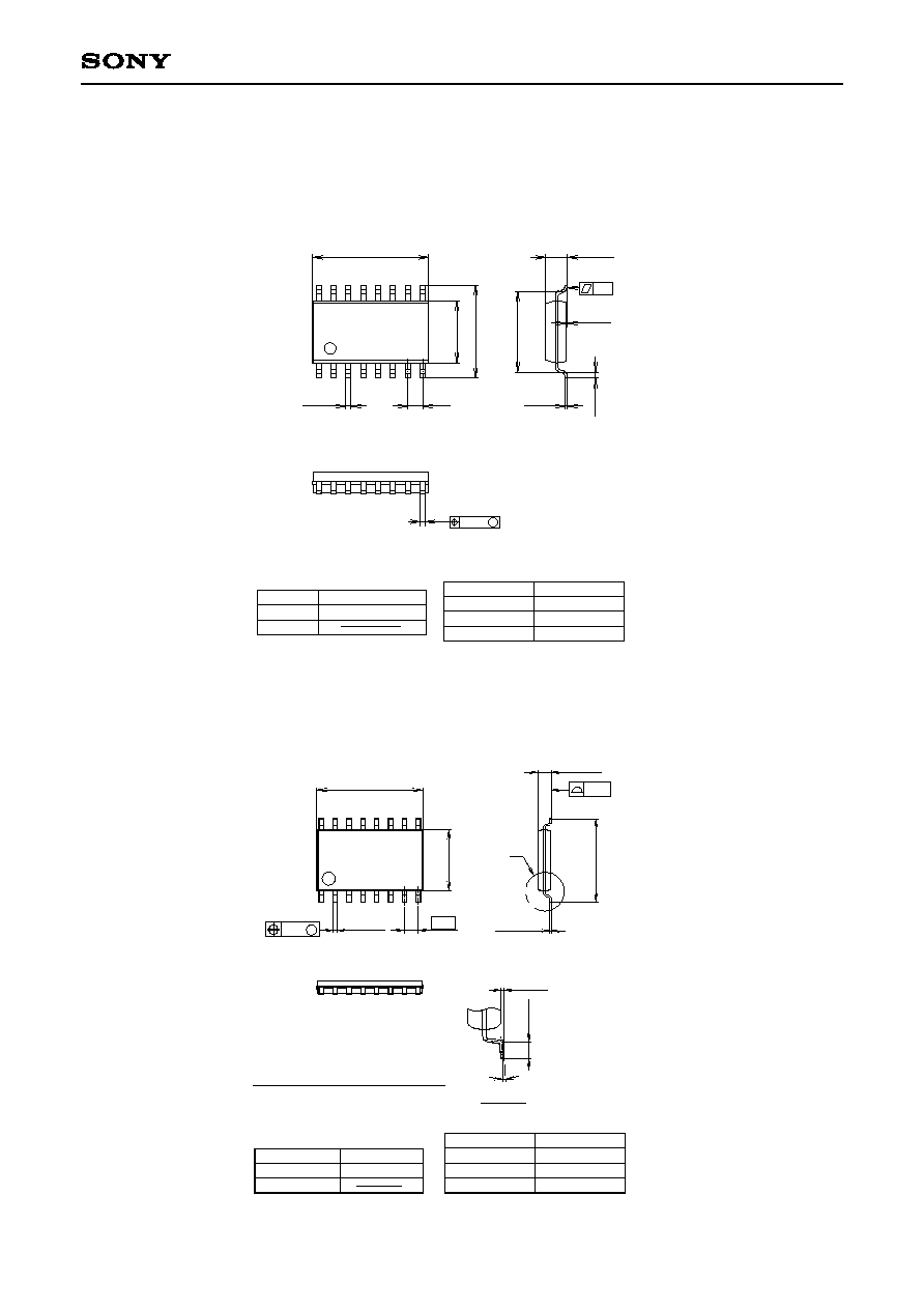
Package Outline
Unit: mm
CXA1665AM
PACKAGE STRUCTURE
PACKAGE MATERIAL
LEAD TREATMENT
LEAD MATERIAL
PACKAGE WEIGHT
SONY CODE
EIAJ CODE
JEDEC CODE
SOP-16P-L01
SOP016-P-0300-A
COPPER ALLOY
SOLDER PLATING
EPOXY RESIN
16PIN SOP (PLASTIC) 300mil
9.9 ≠ 0.1
+ 0.4
16
9
1
8
1.27
0.45 Ī 0.1
5.3 ≠ 0.1
+ 0.3
7.9 Ī
0.4
6.9
1.85 ≠ 0.15
+ 0.4
0.5 Ī
0.2
0.2 ≠ 0.05
+ 0.1
0.1 ≠ 0.05
+ 0.2
0.2g
0.15
M
Ī 0.12
CXA1665AM-S
SONY CODE
EIAJ CODE
JEDEC CODE
SOP-16P-L04
SOP016-P-0300
PACKAGE MATERIAL
LEAD TREATMENT
LEAD MATERIAL
PACKAGE WEIGHT
EPOXY RESIN
SOLDER/PALLADIUM
COPPER ALLOY
PACKAGE STRUCTURE
PLATING
0.1g
16PIN SOP(PLASTIC)
0.1
0į to 10į
DETAIL A
NOTE: "
" Dimensions do not include mold protrusion.
0.12 M
16
9
9.7 Ī 0.1
5.6 Ī
0.1
0.4 ≠ 0.05
+ 0.1
1.27
1
8
0.15 ≠ 0.02
+ 0.05
A
1.25 ≠ 0.1
+ 0.2
0.5 Ī
0.2
0.1 Ī 0.1
7.6 Ī
0.2