 | –≠–ª–µ–∫—Ç—Ä–æ–Ω–Ω—ã–π –∫–æ–º–ø–æ–Ω–µ–Ω—Ç: CXA1720Q | –°–∫–∞—á–∞—Ç—å:  PDF PDF  ZIP ZIP |

Block Diagram and Pin Configuration
--1--
E93717-TE
Read/Write Amplifier (with Built-in Filters) for FDDs
32 pin QFP (Plastic)
CXA1720Q
∑ Supply voltage detection circuit prohibits error
writing during power ON/OFF or abnormal voltage.
∑ Power consumption is kept down to 115 mW (typ.)
and this IC is suitable for use with battery-driven
FDDs.
∑ Built in Time constant capacitors for monostable
multivibrator Nos. 1 and 2. (The pulse width for
monostable multivibrator No. 2 is fixed.)
∑ Power saving function reduces power consumption
when the IC is not in use. When in power saving
mode (5 mW typ.), only the power supply ON/OFF
detector functions.
∑ The Write driver has a built-in reset circuit. When
the mode is switched from Read mode to Write
mode, the Write current flows from head 0A if head
side 0 is selected and from head 1A if head side 1
is selected.
Description
The CXA1720Q is an IC for use with floppy disk
drives, and contains a Read circuit (with built-in
filters), Write circuit, Erase circuit, and supply
voltage detection circuit, all into a single chip.
Features
∑ Single 5 V power supply.
∑ Filter system can be switched among four modes:
1M/2M, and inner track/outer track. This allows for
a significant reduction in the number of external
parts such as differentiator constants, low-pass
filters, and switches. (Compared with conventional
Sony products, the number of parts has been
reduced by one-half.)
∑ Filter characteristics can be customized.
∑ Low pre-amplifier input conversion noise voltage of
2.0 nV/
Hz (typ.) keeps Read data output jitter to
a minimum. The pre-amplifier voltage gain can be
selected as either 100
◊
or 200
◊
.
∑ The monostable multivibrator No. 1 pulse width
switching function for the time domain filter permits
switching between 1M and 2M mode.
∑ Write current switching function permits switching
of the Write current among four modes: 1M/2M
and inner track/outer track. (Filter inner track/outer
track switching is separate.)
FILTER
OUT B
COMP
IN B
COMP
IN A
A.GND
MMVA
FILTER
SET
Vcc
HIGH
DENSITY
POWER
ON
WRITE
DATA
READ DATA
WRITE
CURRENT
WRITE
GATE
ERASE
GATE
SIDE 1
FILTER
CONTROL
W/C 1
SET
W/C 1
COMP
W/C 2
SET
W/C 2
COMP
ERASE
OUT 0
ERASE
OUT 1
HEAD 0A
HEAD 0B
HEAD 1A
HEAD 1B
PREAMP OUT
VREF
FILTER OUT A
WRITE
DRIVER
ERASE
DRIVER
POWER
MONITOR
CONTROL
LOGIC
TIME
DOMAIN
FILTER
COMP
FILTER
DIFF+LPF
(BPF)
1
2
3
4
5
6
7
8
16
15
14
13
12
9
10
11
22
21
20
19
18
17
23
24
HIGH
GAIN
25
26
27
28
29
30
31
32
D.GND
POWER
SAVE
PREAMP
Sony reserves the right to change products and specifications without prior notice. This information does not convey any license by
any implication or otherwise under any patents or other right. Application circuits shown, if any, are typical examples illustrating the
operation of the devices. Sony cannot assume responsibility for any problems arising out of the use of these circuits.
For the availability of this product, please contact the sales office.

--2--
CXA1720Q
Structure
Bipolar silicon monolithic IC
Absolute Maximum Ratings (Ta=25 ∞C)
∑ Supply voltage
V
CC
7
V
∑ Digital signal input pin (note) input voltage
≠0.5 to V
CC
+0.3
V
∑ Power ON output applied voltage
V
CC
+0.3
V
∑ Erase output applied voltage
V
CC
+0.3
V
∑ Head 0A, 0B, 1A, 1B applied voltage
15
V
∑ Power ON output sink current
7
mA
∑ Erase output sink current
30
mA
∑ Operating temperature
Topr
≠20 to +75
∞C
∑ Storage temperature
Tstg
≠65 to +150
∞C
∑ Allowable power dissipation
P
D
500
mW
Supply Voltage Range
V
CC
4.4 to 6.0
V
Note) WRITE DATA, WRITE CURRENT, WRITE GATE, ERASE GATE
SIDE1, FILTER CONTROL, HIGH DENSITY, HIGH GAIN, POWER SAVE
--3--
CXA1720Q
Pin Description
(Ta=25 ∞C, V
CC
=5 V)
Vcc
A.GND
1k
2
2.3V
Vcc
D.GND
140
3
Vcc
A.GND
1k
100k
2.1V
4
5
6
8
9
20
7
Pin
Symbol
Pin voltage
Equivalent circuit
Description
No.
1
2
3
4
5
6
7
8
9
20
POWER ON
WRITE
DATA
READ
DATA
WRITE
CURRENT
WRITE
GATE
ERASE
GATE
SIDE1
FILTER
CONTROL
HIGH
DENSITY
HIGH
GAIN
--
--
--
--
--
--
--
--
--
--
Vcc
A.GND
100k
1
Reduced voltage detection output.
This is an open collector that outputs a low signal
when V
CC
is below the specified value.
Write data input.
This pin is a Schmitt-type input and is triggered
when the logical voltage goes from high to low.
Read data output.
This pin is active when the logical voltage of the
Write gate signal and the Erase gate signal is high.
Write current control. The Write current is
increased when the logical voltage is low.
Write gate signal input. The Write system is active
when the logical voltage is low.
Erase gate signal input. The Erase system is
active when the logical voltage is low.
Head side switching signal input. The HEAD1
system is active when the logical voltage is low,
and the HEAD0 system is active when the logical
voltage is high, but only when the logical voltage
for the Write gate and the Erase gate is high.
Filter inner track/outer track mode control. Inner
track mode is selected when the logical voltage is
low.
Filter, time domain filter and Write current 1M/2M
mode control. 2M mode is selected when the
logical voltage is low.
Pre-amplifier voltage gain selection. Gain of 100x
is selected when the logical voltage is high; gain of
200x is selected when the logical voltage is low.
--4--
CXA1720Q
Vcc
A.GND
147
1.2V
12
Vcc
A.GND
14
15
147
147
10k
10k
16k
60µ
Vcc
A.GND
140
16
17
500µ
140
500µ
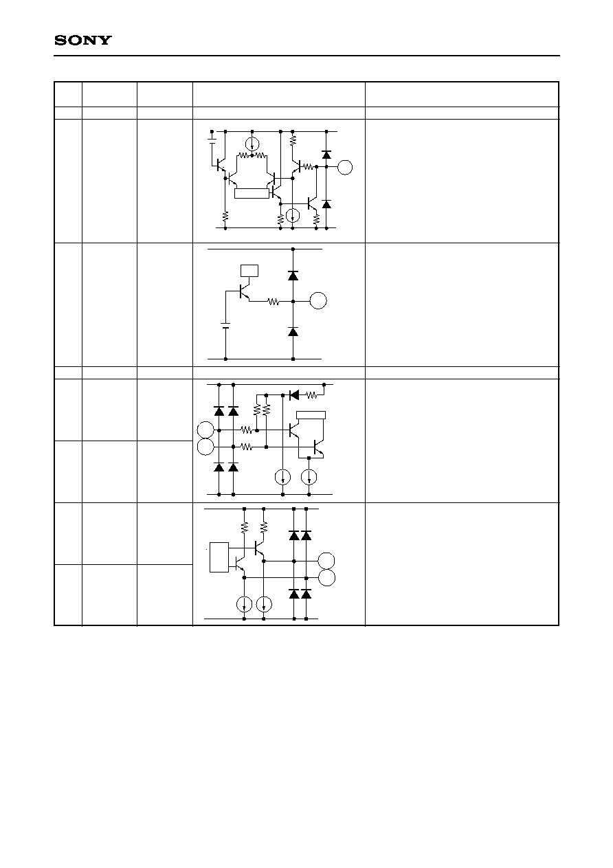
Pin
Symbol
Pin voltage
Equivalent circuit
Description
No.
10
11
12
13
14
15
16
17
V
CC
FILTER
SET
MMVA
A. GND
COMP IN A
COMP IN B
FILTER
OUT B
FILTER
OUT A
--
3.8 V
0.5 V
--
3.3 V
3.3 V
3.3 V
3.3 V
Vcc
A.GND
147
11
1.2V
1k
Power supply (5 V) connection.
Connection for filter cut-off frequency setting
resistor. Connect the filter cut-off frequency setting
resistor R
F
between this pin and V
CC
to set the cut-
off frequency.
Time domain filter monostable multivibrator No. 1
pulse width setting pin. Connect the monostable
multivibrator No. 1 pulse width setting resistor R
A
between this pin and A.GND.
Analog system GND connection.
Comparator differential inputs.
Filter differential outputs.

--5--
CXA1720Q
Vcc
A.GND
140
320µ
19
A.GND
24
23 22
21
Vcc
A.GND
1.2V
25
27
147
147
Vcc
A.GND
28
26
Pin
Symbol
Pin voltage
Equivalent circuit
Description
No.
18
19
21
22
23
24
25
27
26
28
VREF
PREAMP
OUT
HEAD 1B
HEAD 1A
HEAD 0B
HEAD 0A
W/C1SET
W/C2SET
W/C1
COMP
W/C2
COMP
2.8 V
2.8 V
--
--
--
--
--
--
Vcc
A.GND
500
120µ
18
Connection for internal reference voltage
decoupling capacitor. Connect the decoupling
capacitor CREF between this pin and A.GND.
Pre-amplifier output.
Connection for magnetic head input/output.
Connect the recording/playback magnetic head to
these pins, and connect the center tap to V
CC
.
When the logical voltage for Pin 7 (SIDE1) is low,
the HEAD1 system is active; when the logical
voltage is high, the HEAD0 system is active.
Connection for 1M write current setting resistor.
Connect the Write current setting resistor R
W1
between this pin and V
CC
to set the Write current.
Connection for 2M Write current setting resistor.
Connect the Write current setting resistor R
W2
between this pin and V
CC
to set the Write current.
Connection for 1M Write current compensation
resistor.
Connect the Write current compensation resistor
R
WC1
between this pin and Pin 25 (W/C1SET) to
set the amount of increase in the Write current.
Connection for 2M Write current compensation
resistor.
Connect the Write current compensation resistor
R
WC2
between this pin and Pin 27 (W/C2SET) to
set the amount of increase in the Write current.

--6--
CXA1720Q
Vcc
A.GND
1k
162k
2.1V
32
Pin
Symbol
Pin voltage
Equivalent circuit
Description
No.
29
30
31
32
D. GND
ERASE
OUT0
ERASE
OUT1
POWER
SAVE
--
--
--
--
Vcc
D.GND
30
31
Digital system GND connection.
Erase current output for the HEAD0 system.
Erase current output for the HEAD1 system.
Power saving signal input.
When the logical voltage is low, the IC is in power
saving mode. In power saving mode, only the
power supply ON/OFF detection function operates.

--7--
CXA1720Q
Electrical Characteristics
Current Consumption
(Ta=25 ∞C, V
CC
=V)
Power Supply Monitoring System
(Ta=25 ∞C)
Read System
When SW4 = a: Vi = 10 mVp-p
When SW4 = b: Vi = 5 mVp-p
Measure- Measure-
Item
Symbol
Conditions
ment
ment
Min.
Typ.
Max.
Unit
circuit
point
Current consumption for Read
ICCR
V
CC
=5 V
--
--
13.0
23.0
33.0
WG="H"
Current consumption for
ICCWE
V
CC
=5 V
--
--
8.0
14.0
20.0
mA
Write/Erase
WG="L", EG="L"
Current consumption for
ICCPS
V
CC
=5 V
--
--
0.9
1.8
Power saving
PS="L"
Measure- Measure-
Item
Symbol
Conditions
ment
ment
Min.
Typ.
Max.
Unit
circuit
point
Power supply ON/OFF detector
VTH
--
--
3.5
3.9
4.3
threshold voltage
V
Power ON output saturation
VSP
V
CC
=3.5 V
--
--
0.5
voltage
I=1 mA
Measure- Measure-
Item
Symbol
Conditions
ment
ment
Min.
Typ.
Max.
Unit
circuit
point
Pre-amplifier voltage gain
GV0
f=100 kHz
SIDE0
SW4=a, b
38.1/
41.6/
Pre-amplifier voltage gain
f=100 kHz
1
G
44.1
40/46
47.6
dB
SIDE1
GV1
SW4=a, b
SW1, 5=b
Pre-amplifier frequency response
BW0
A
V
/A
V0
=≠3 dB
SIDE0
SW4=a, b
Pre-amplifier frequency response
A
V
/A
V1
=≠3 dB
1
G
5
MHz
SIDE1
BW1
SW4=a, b
SW1, 5=b
Pre-amplifier input conversion
Bandwidth=400 Hz
noise voltage
EN0
to 1 MHz Vi=0,
SIDE0
SW4=b
Pre-amplifier input conversion
Bandwidth=400 Hz
1
G
2.0
2.9
µ
Vrms
noise voltage
EN1
to 1 MHz
SIDE1
SW4=b
Vi=0, SW1, 5=b
--8--
CXA1720Q
Read System
(Ta=25 ∞C, V
CC
=5 V)
When SW4 = a: Vi = 60 mVp-p
When SW4 = b: Vi = 30 mVp-p
Read data output between 0.5 V to 2.4 V
For Vi = 0.25 mVp-p to 5m Vp-p: SW4 = b (pre-amplifier voltage gain: 46 dB)
For Vi = 0.5 mVp-p to 10 mVp-p: SW4 = a (pre-amplifier voltage gain: 40 dB)
Measure- Measure-
Item
Symbol
Conditions
ment
ment
Min.
Typ.
Max.
Unit
circuit
point
Pre-amplifier output offset voltage
Vi=0
(vs. VREF)
VOFSP SW4=a, b,
1
F, G
≠500
+500
mV
SW1, 5=a, b
Pre-amplifier output voltage
f=100 kHz
amplitude
VOP
SW4=a, b,
1
G
1.8
Vp-p
SW1, 5=a, b
Filter differential output offset
VOFSF Vi=0
1
D, E
≠100
+100
mV
voltage
Filter differential output voltage
VOF
f=100 kHz
1
D, E
2.8
Vp-p
amplitude
Vi=60 mVp-p
Time domain filter monostable
ETM1
R
A
=27 k
B, C
multivibrator No. 1 pulse width
ETM1'
Refer to Fig. 1
1
A
≠10
+10
%
precision
Time domain filter monostable
R
A
=27 k
multivibrator No. 2 pulse width
T2
Refer to Fig. 1
1
A
260
400
540
ns
(fixed)
Read data output low voltage
VOL
I
OL
=2 mA
1
A
0.5
V
Read data output high voltage
VOH
I
OH
=≠0.4 mA
1
A
2.8
V
Read data output
rise time
TR
R
L
=2 k
1
A
100
ns
C
L
=20 pF
Read data output
fall time
TF
R
L
=2 k
1
A
100
ns
C
L
=20 pF
Vi=0.25 mVp-p to
Peak shift
PS
10 mVp-p
1
A
1
%
f=62.5 kHz
Refer to Fig. 1

--9--
CXA1720Q
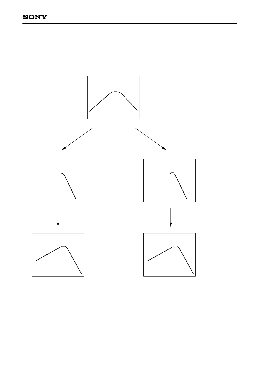
Fig. 1 Monostable multivibrator Nos. 1 and 2 pulse width precision and peak shift measurement conditions
∑ Monostable multivibrator No. 1 pulse width precision
When HD = high:
ETM1 =
(
T
1
≠1
)
◊
100 (%)
2.45 µS
When HD is low:
ETM1' =
(
T
1
≠1
)
◊
100 (%)
1.25 µS
∑ Monostable multivibrator No. 2 pulse width = T
2
∑ Peak shift
PS =
1
T
A
≠T
B
◊
100 (%)
2
T
A
+T
B
Comparator input
(Measurement points B and C)
Read data output
(Measurement point A)
T1
T2
TA
TB
1.4V

--10--
CXA1720Q
Read System (Filters)
(Ta=25 ∞C, V
CC
=5 V)
G
PN
= 20Log
10
(V
Filterout
/V
Preout
)
V
Filterout
: Filter differential output voltage
(N=1 to 4)
Measure- Measure-
Item
Symbol
Conditions
ment
ment
Min.
Typ.
Max.
Unit
circuit
point
Peak frequency
F
O1
Vi=3mVp-p HG="L"
1
D, E
153.0
170.0
187.0
kHz
HD="H" FC="H"
Peak voltage gain
G
P1
Refer to Fig. 2
1
G
3.6
5.5
7.1
1M/
at f
O1
D, E
outer
Refer to Fig. 2
track
Frequency response (1)
G
11
at
1
f
O1
1
D, E
≠7.6
≠7.1
≠6.6
dB
3
Frequency response (2)
G
12
Refer to Fig. 2
1
D, E
≠25.0
≠23.1
≠21.5
at 3f
O1
Vi=3mVp-p
Peak frequency
f
O2
HG=":L"
1
D, E
163.8
182.0
200.2
kHz
HD="H" FC="L"
1M/
Peak voltage gain
G
P2
Refer to Fig. 2
1
G
3.6
5.5
7.1
inner
at f
O2
D, E
track
Refer to Fig. 2
Frequency response (1)
G
21
at
1
f
O2
1
D, E
≠7.6
≠7.1
≠6.6
dB
3
Frequency response (2)
G
22
Refer to Fig. 2
1
D, E
≠25.0
≠23.1
≠21.5
at 3f
O2
Peak frequency
f
O3
Vi=3mVp-p HG="L"
1
D, E
288.0
320.0
352.0
kHz
HD="L" FC="H"
Peak voltage gain
G
P3
Refer to Fig. 2
1
G
3.6
5.5
7.1
2M/
at f
O3
D, E
outer
Refer to Fig. 2
track
Frequency response (1)
G
31
at
1
f
O3
1
D, E
≠7.6
≠7.1
≠6.6
dB
3
Frequency response (2)
G
32
Refer to Fig. 2
1
D, E
≠25.0
≠23.1
≠21.5
at 3f
O3
Peak frequency
f
O4
Vi=3mVp-p HG="L"
1
D, E
310.5
345.0
379.5
kHz
HD="L" FC="L"
Peak voltage gain
G
P4
Refer to Fig. 2
1
G
5.3
7.2
8.8
2M
at f
O4
D, E
inner
Refer to Fig. 2
track
Frequency response (1)
G
41
at
1
f
O4
1
D, E
≠8.6
≠8.1
≠7.6
dB
3
Frequency response (2)
G
42
Refer to Fig. 2
1
D, E
≠36.2
≠34.3
≠32.7
at 3f
O4

(dB)
G
PN
G
1N
1
3
f
0
f
0
3f
0
f(Hz)
G
2N
(N=1 to 4)
--11--
CXA1720Q
Fig. 2 Filter frequency response measurement conditions
--12--
CXA1720Q
Write/Erase System
(Ta=25 ∞C, V
CC
=5 V)
Write current output precision
E
W
=
(
I
W
≠1
)
◊
100 (%)
2.70 mA
Write current compensation current precision
E
WC
=
(
I
W
'≠I
W
≠1
)
◊
100 (%)
0.90 mA
I
W
: WRITE CURRENT = "H" I
W
': WRITE CURRENT = "L"
Logic Input Block
Measure- Measure-
Item
Symbol
Conditions
ment
ment
Min.
Typ.
Max.
Unit
circuit
point
Write current output precision
EW
WG="L"
2
LKJI
≠7
+7
R
W
=4.3 k
Write current output unbalance
DW
WG="L"
2
LKJI
≠1
+1
R
W
=4.3 k
%
Write current compensation current
WG="L"
precision
EWC
R
W
=4.3 k
2
LKJI
≠10
+10
R
WC
=12 k
Head I/O pin leak current for Write
ILKW
WG="L"
2
LKJI
10
µA
Head I/O pin saturation voltage
VSW
WG="L"
2
L'K'J'I'
1
V
for Write
SW1=6
Leak current for Erase current
ILKE
EG="L"
2
MN
10
µA
switch
Output saturation voltage for Erase
EG="L"
current switch
VSE
I=30 mA
2
M'N'
500
mV
SW2=b
Measure- Measure-
Item
Symbol
Conditions
ment
ment
Min.
Typ.
Max.
Unit
circuit
point
Digital low input voltage
VLD
2
BCDE
0.8
FGHP
Digital high input voltage
VHD
2
BCDE
2.0
FGHP
V
Schmitt-type digital low input
VLSD
2
A
0.8
voltage
Schmitt-type digital high input
VHSD
2
A
2.0
voltage
Digital low input current
ILD
V
L
=0 V
2
ABCD
≠20
EFGHP
µA
Digital high input current
IHD
V
H
=5 V
2
ABCD
10
EFGHP
--13--
CXA1720Q
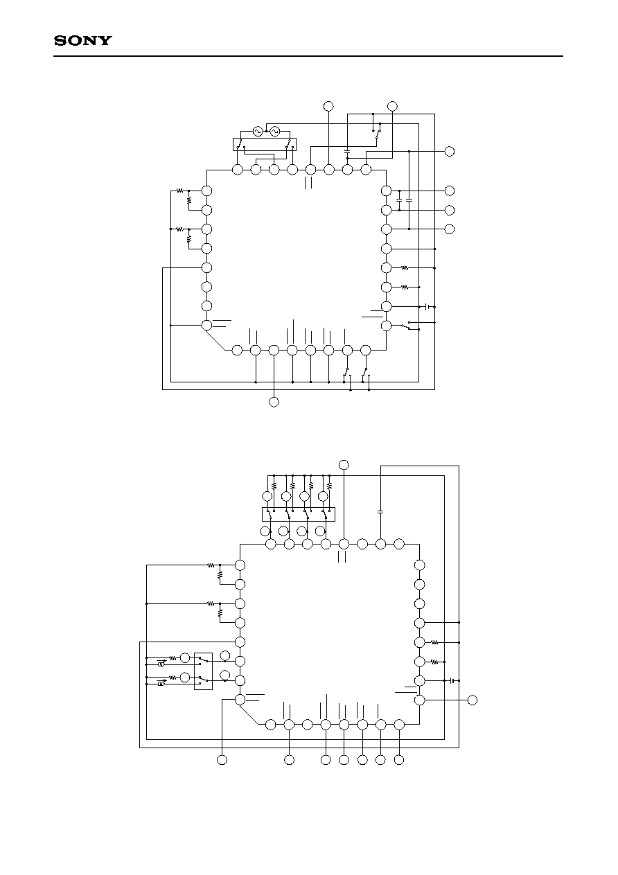
Electrical Characteristics Measurement Circuit 1
Note) Unless otherwise specified, switches are assumed to be set to "a".
Electrical Characteristics Measurement Circuit 2
Note) Unless otherwise specified, switches are assumed to be set to "a".
1
2
3
4
5
6
7
8
22
21
20
19
18
17
23
24
16
15
14
13
12
9
10
11
25
26
27
28
29
30
31
32
FILTER
OUT B
COMP
IN B
COMP
IN A
A.GND
MMVA
FILTER
SET
Vcc
P
O
W
E
R
O
N
W
R
I
T
E
D
A
T
A
R
E
A
D
D
A
T
A
W
R
I
T
E
C
U
R
R
E
N
T
W
R
I
T
E
G
A
T
E
E
R
A
S
E
G
A
T
E
F
I
L
T
E
R
C
O
N
T
R
O
L
W/C 1
SET
W/C 1
COMP
W/C 2
SET
W/C 2
COMP
D.GND
ERASE
OUT 0
ERASE
OUT 1
H
E
A
D
0
A
H
E
A
D
0
B
H
E
A
D
1
A
H
E
A
D
1
B
P
R
E
A
M
P
O
U
T
V
R
E
F
F
I
L
T
E
R
O
U
T
A
CXA1720Q
C
B
A
D
G
F
E
0.1µ
a
b
SW4
1/2V 1
≠1/2V 1
SW5
a
b
a
b
4.3k
12k
4.3k
12k
SW1
SW2
a
b
a
b
SW3
a
b
3.2k
27k
5V
3300p
3300p
POWER
SAVE
HIGH
DENSITY
H
I
G
H
G
A
I
N
S
I
D
E
1
G
4.3k
12k
4.3k
12k
3.2k
27k
5V
0.1µ
L
K
J
I
H
2.2k
SW1 a
b
2.2k
2.2k
2.2k
a
b
a
b a
b
1
2
3
4
5
6
7
8
22
21
20
19
18
17
23
24
16
15
14
13
12
9
10
11
25
26
27
28
29
30
31
32
FILTER
OUT B
COMP
IN B
COMP
IN A
A.GND
MMVA
FILTER
SET
Vcc
P
O
W
E
R
O
N
R
E
A
D
D
A
T
A
W
R
I
T
E
C
U
R
R
E
N
T
W
R
I
T
E
G
A
T
E
E
R
A
S
E
G
A
T
E
S
I
D
E
1
F
I
L
T
E
R
C
O
N
T
R
O
L
W/C 1
SET
W/C 1
COMP
W/C 2
SET
W/C 2
COMP
D.GND
ERASE
OUT 0
ERASE
OUT 1
H
E
A
D
0
A
H
E
A
D
0
B
H
E
A
D
1
A
H
E
A
D
1
B
P
R
E
A
M
P
O
U
T
V
R
E
F
F
I
L
T
E
R
O
U
T
A
CXA1720Q
L'
K'
J'
I'
P
A
B
C
D
E
F
M
N
100k
30mA
a
b
SW2
100k
30mA
a
b
M'
N'
H
I
G
H
G
A
I
N
POWER
SAVE
W
R
I
T
E
D
A
T
A
HIGH
DENSITY

--14--
CXA1720Q
Description of Operation
(1) Read system
Pre-amplifier
The pre-amplifier amplifies input signals. The voltage gain can be switched between 40 dB and 46 dB,
using Pin 20.
Filters
The filters differentiate the signals amplified by the pre-amplifier. The high-band noise components are
attenuated by the low-pass filter. The filters can be switched among four modes, depending on the
settings of Pins 8 and 9. In 1M/outer track mode, the peak frequency f
O1
is set by external resistor R
F
.
f
O
for the other three modes is switched by the internal settings of the IC, with f
O1
used as a reference
(1.00).
The filters are explained below.
1) Active filter block
Filter Characteristics
Table 1
The formula for the peak frequency f
01
for 1M/outer track mode is shown below:
f
01
= 527/R
F
+ 5.8 (kHz)
f
01
: peak frequency in 1M/outer track mode
R
F
: filter setting resistance (k
)
The relationship between f01 and f0 in the four modes is as follows:
1M/outer track: f
01
= 1.0
◊
f
01
1M/inner track: f
02
= 1.07
◊
f
01
2M/outer track: f
03
= 1.88
◊
f
01
2M/inner track: f
04
= 2.03
◊
f
01
Note that these filters can be customized.
Customization is explained on pages 17 and 18.
17
16
19
BPF
LPF
HPF
Amp.
Pre-amplifier output
Secondary
Tertiary
Primary
Filter output A
Filter output B
f
OB
=1.2Xf
CL
f
CL
; variable
f
CH
=5KHz
Gain; 8.0dB
Q=0.577
Q; variable
Pre-amplifier output
Pin 8
Pin 9
LPF characteristics
f
O
ratio
H
H
1M/outer track mode: Butterworth
1.00
L
H
1M/inner track mode: Butterworth
1.07
H
L
2M/outer track mode: Butterworth
1.88
L
L
2M/inner track mode: Chebyshev 1 dB ripple
2.03

--15--
CXA1720Q
Comparator
The comparator detects the crosspoint of the filter differential output.
Time domain filter
The time domain filter converts the comparator output to Read data.
This filter is equipped with two monostable multivibrators. Monostable multivibrator No. 1 eliminates
unnecessary pulses, and monostable multivibrator No. 2 determines the pulse width of Read data.
The monostable multivibrator No. 1 pulse width T
A
is determined by the resistor R
A
between Pin 12 and
A.GND. T
A
can be switched as follows by the setting of Pin 9:
HIGH DENSITY = "H"
T
A LOW
= 84R
A
+ 180 (nS)
R
A
(k
)
HIGH DENSITY = "L"
T
A HIGH
= 42R
A
+ 110 (nS)
The pulse width for monostable multivibrator No. 2 is fixed at 400 ns.
(2) Write System
Write data input through Pin 2 is frequency-divided by the T flip-flop and generates the head recording
current. The recording current can be switched by the setting of Pin 9.
The Write current Iw is set by the resistor R
W
connected between Pin 25 and V
CC
and between Pin 27 and
V
CC
.
I
W
= 11.6/R
W
(mA)
R
W
(k
)
Furthermore, the Write current compensation I
WC
is set by the resistor R
WC
connected between Pin 25 and Pin
26, and between Pin 27 and Pin 28.
I
WC
= 10.8/R
WC
(mA)
R
WC
(k
)
(3) Erase System
Pins 30 and 31 are open collector outputs; the Erase current is set by the resistance between these pins
and the Erase head.
(4) Power ON/OFF Detection System
The power ON/OFF detection system detects a reduced voltage.
When V
CC
is below the stipulated voltage, the Write system and Erase system cease operation, disabling
the Write and Erase functions
Notes on Operation
∑ Select the voltage gain so that the pre-amplifier output amplitude is 1 Vp-p or less.
If the pre-amplifier output amplitude exceeds 1 Vp-p, the filter output waveform becomes distorted.
∑ Observe the following points when mounting this IC.
∑ Connect a V
CC
decoupling capacitor of approximately 0.1 µF close to the IC.
∑ The ground should be as large as possible.

--16--
CXA1720Q
Application Circuit (for 1M/2M devices)
FILTER
OUT B
COMP
IN B
COMP
IN A
A.GND
MMVA
FILTER
SET
Vcc
HIGH
DENSITY
POWER
ON
WRITE
DATA
READ
DATA
WRITE
CURRENT
WRITE
GATE
ERASE
GATE
SIDE 1
FILTER
CONTROL
W/C 1SET
W/C 1COMP
W/C 2
SET
W/C 2
COMP
D.GND
ERASE
OUT 0
ERASE
OUT 1
POWER
SAVE
HEAD
0A
HEAD
0B
HEAD
1A
PREAMP
OUT
VREF
FILTER
OUT A
WRITE
DRIVER
ERASE
DRIVER
POWER
MONITOR
CONTROL
LOGIC
T
I
M
E
D
O
M
A
I
N
F
I
L
T
E
R
C
O
M
P
FILTER
DIFF+LPF
(BPF)
PREAMP
1
2
3
4
5
6
7
8
16
15
14
13
12
9
10
11
22
21
20
19
18
17
23
24
R
A
27k
R
F
3.2k
5V
C
B
3300P
C
A
3300P
C
REF
0.1µ
25
26
27
28
29
30
31
32
R
E0
R
E1
R
W1
R
W2
R
W
C
1
R
W
C
2
HEAD
1B
HIGH
GAIN
Application circuits shown are typical examples illustrating the operation of the devices. Sony cannot assume responsibility for
any problems arising out of the use of these circuits or for any infringement of third party patent and other right due to same.
--17--
CXA1720Q
Customization
Filter frequency response
In 2M/inner track mode, the filter frequency response can be changed as shown below.
B. P. F
Q=0.577
(Differential characteristics)
L. P. F
Tertiary
Butterworth
No. 2
L. P. F
Tertiary Chebyshev
1dBRp
(High-band noise cut-off)
(Comprehensive characteristics)
No. 3

--18--
CXA1720Q
Filter Customization Selections/Combinations
In filter settings, use the LPF cut-off frequency f
C1
in 1M/outer track mode as 1.00 as shown in Table 1 to
select fc ratios and LPF types for the other three modes. The 1M/outer track to 2M/outer track modes for the
LPF are fixed to Butterworth, while either Butterworth or Chebyshev 1 dB ripple can be selected in 2M/inner
track mode.
Note that the BPF center frequency f
oB
is fixed at 1.2 times the LPF cut-off frequency fc. In addition, the
relationship between the peak frequencies fo and fc in regards to the comprehensive characteristics is as
follows, depending on differences in LPFs.
Butterworth characteristics:
f
C
= 1.28fo
Chebyshev 1 dB ripple characteristics:
f
C
= 1.12fo
Table 1 LPF fc Ratios and Types
Note) The boxed item indicates the setting for the CXA1720Q.
Mode
LPF type
f
c
ratio when f
c1
is assumed as 1.00
1M/outer track
Butterworth
1.00
1.07
1.14
1.23
1.33
1.45
1M/inner track
Butterworth
1.60
2.00
1.33
1.39
1.45
1.52
1.60
2M/outer track
Butterworth
1.68
1.78
1.88
2.00
2.13
2.29
2.46
2.67
Butterworth
1.33
1.39
1.45
1.52
1.60
2M/inner track
Chebyshev
1.68
1.78
1.88
2.00
2.13
(1 dB ripple)
2.29
2.46
2.67

--19--
CXA1720Q
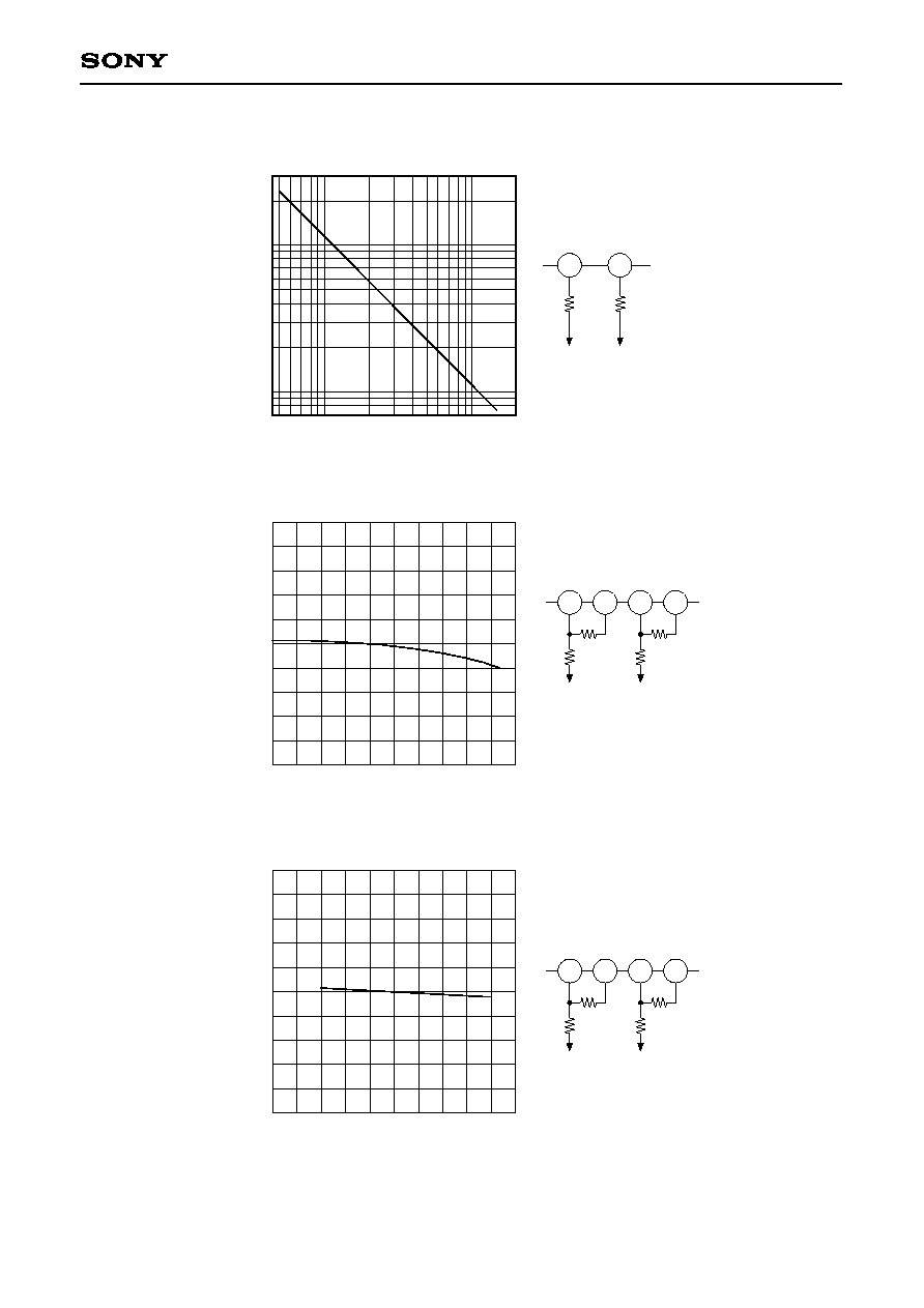
Normalized pre-amplifier voltage gain and phase vs. Frequency
Vcc=5V, Ta=25∞C
When HD=high, low
N
o
r
m
a
l
i
z
e
d
p
r
e
-
a
m
p
l
i
f
i
e
r
v
o
l
t
a
g
e
g
a
i
n
(
d
B
)
f-Frequency (Hz)
P
h
a
s
e
(
d
e
g
r
e
e
)
Phase
Voltage Gain
Filter characteristics in the four modes
(These characteristics are based on pre-amplifier output. 0dB=pre-amplifier output
level)
0
≠2
≠4
≠6
≠8
≠10
10k
100k
1M
10M
100M
0
30
60
90
120
150
1M/outer track
N
o
r
m
a
l
i
z
e
d
f
i
l
t
e
r
v
o
l
t
a
g
e
g
a
i
n
(
d
B
)
f
01
=170 (KHz) Frequency (Hz)
P
h
a
s
e
(
d
e
g
r
e
e
)
Voltage gain
Phase
10k
50k
100k
300k
1M
3M
10
0
≠10
≠20
≠30
≠40
≠50
≠60
≠70
200
150
100
50
0
≠50
≠100
≠200
≠150
1M/inner track
N
o
r
m
a
l
i
z
e
d
f
i
l
t
e
r
v
o
l
t
a
g
e
g
a
i
n
(
d
B
)
f
02
=182 (KHz) Frequency (Hz)
P
h
a
s
e
(
d
e
g
r
e
e
)
Voltage gain
Phase
10k
50k
100k
300k
1M
3M
10
0
≠10
≠20
≠30
≠40
≠50
≠60
≠70
200
150
100
50
0
≠50
≠100
≠200
≠150
2M/outer track
N
o
r
m
a
l
i
z
e
d
f
i
l
t
e
r
v
o
l
t
a
g
e
g
a
i
n
(
d
B
)
f
03
=320 (KHz) Frequency (Hz)
P
h
a
s
e
(
d
e
g
r
e
e
)
Voltage gain
Phase
10k
50k
100k
300k
1M
3M
10
0
≠10
≠20
≠30
≠40
≠50
≠60
≠70
200
150
100
50
0
≠50
≠100
≠200
≠150
2M/inner track
N
o
r
m
a
l
i
z
e
d
f
i
l
t
e
r
v
o
l
t
a
g
e
g
a
i
n
(
d
B
)
f
04
=345 (KHz) Frequency (Hz)
P
h
a
s
e
(
d
e
g
r
e
e
)
Voltage gain
Phase
10k
50k
100k
300k
1M
3M
10
0
≠10
≠20
≠30
≠40
≠50
≠60
≠70
200
150
100
50
0
≠50
≠100
≠200
≠150
V
CC
=5V, Ta=25∞C
R
F
=3.2k
V
CC
=5V, Ta=25∞C
R
F
=3.2k
V
CC
=5V, Ta=25∞C
R
F
=3.2k
V
CC
=5V, Ta=25∞C
R
F
=3.2k

--20--
CXA1720Q
Normalized pre-amplifier voltage gain+filter voltage gain
vs. Ambient temperature
Ta-Ambient temperature (∞C)
f=100KHz Vcc=5V
Vin=10mVp-p (HG="H")
Vin=5mVp-p (HG="L")
NGV=GV/GV (Ta=25∞C)
1.50
1.00
0.50
≠20
0
20
40
60
80
11
Normalized pre-amplifier voltage gain+filter voltage gain
vs. Supply voltage
Vcc-Supply voltage (V)
Ta=25∞C
f=100KHz
Vin=10mVp-p (HG="H")
Vin=5mVp-p (HG="L")
NGV=GV/GV (Vcc=5V)
1.50
1.00
0.50
4.0
5.0
6.0
11
R
F
3.2k
Vcc
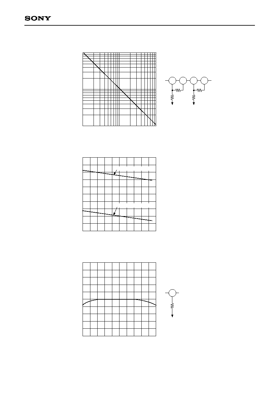
Normalized monostable multivibrator No. 1 pulse width
vs. Ambient temperature
N
T
A
-
N
o
r
m
a
l
i
z
e
d
m
o
n
o
s
t
a
b
l
e
m
u
l
t
i
v
i
b
r
a
t
o
r
N
o
.
1
p
u
l
s
e
w
i
d
t
h
Ta-Ambient temperature (∞C)
Vcc=5V
NTA=TA/TA (Ta=25∞C)
When HD=high, low
1.05
1.00
0.95
12
R
A
27k
≠20
0
20
40
60
80
R
F
3.2k
Vcc
N
G
V
-
N
o
r
m
a
l
i
z
e
d
p
r
e
-
a
m
p
l
i
f
i
e
r
v
o
l
t
a
g
e
g
a
i
n
+
f
i
l
t
e
r
v
o
l
t
a
g
e
g
a
i
n
N
G
V
-
N
o
r
m
a
l
i
z
e
d
p
r
e
-
a
m
p
l
i
f
i
e
r
v
o
l
t
a
g
e
g
a
i
n
+
f
i
l
t
e
r
v
o
l
t
a
g
e
g
a
i
n

--21--
CXA1720Q
Monostable multivibrator No. 1 pulse width vs. R
A
T
A
-
M
o
n
o
s
t
a
b
l
e
m
u
l
t
i
v
i
b
r
a
t
o
r
N
o
.
1
p
u
l
s
e
w
i
d
t
h
(
µ
S
)
R
A
(k
)
Vcc=5V
Ta=25∞C
10
3
5
10
50
100
12
Vcc-Supply voltage (V)
1.05
1.00
0.95
4.0
5.0
6.0
Normalized read data pulse width
vs. Ambient temperature
N
T
B
-
N
o
r
m
a
l
i
z
e
d
r
e
a
d
d
a
t
a
p
u
l
s
e
w
i
d
t
h
Ta-Ambient temperature (∞C)
Vcc=5V
NTB=TB/TB (Ta=25∞C)
1.05
1.00
0.95
12
R
A
27k
≠20
0
20
40
60
80
Normalized monostable multivibrator No. 1 pulse width
vs. Supply voltage
N
T
A
-
N
o
r
m
a
l
i
z
e
d
m
o
n
o
s
t
a
b
l
e
m
u
l
t
i
v
i
b
r
a
t
o
r
N
o
.
1
p
u
l
s
e
w
i
d
t
h
Ta=25∞C
NTA=TA/TA (Ta=25∞C)
When HD=high, low
5
1
0.3
T
A LOW
=84R
A
+
180 (ns)
T
A HIGH
=42R
A
+
110 (ns)
R
A
(k
)
R
A
T
A
LOW
T
A
HIGH

--22--
CXA1720Q
Normalized write current vs. Ambient temperature
N
I
W
-
N
o
r
m
a
l
i
z
e
d
w
r
i
t
e
c
u
r
r
e
n
t
Ta-Ambient temperature (∞C)
Vcc=5V
NIW=IW/IW (Ta=25∞C)
1.05
1.00
0.95
≠20
0
20
40
60
80
25
Normalized read data pulse width
vs. Supply voltage
N
T
B
-
N
o
r
m
a
l
i
z
e
d
r
e
a
d
d
a
t
a
p
u
l
s
e
w
i
d
t
h
Vcc-Supply voltage (V)
Ta=25∞C
NTB=TB/TB (Vcc=5V)
1.05
1.00
0.95
4.0
5.0
6.0
Normalized write current vs. Supply voltage
N
I
W
-
N
o
r
m
a
l
i
z
e
d
w
r
i
e
t
c
u
r
r
e
n
t
Vcc-Supply voltage (V)
1.05
1.00
0.95
4.0
5.0
6.0
26
27
28
R
WC1
R
WC2
12k
12k
R
W1
4.3k
R
W2
4.3k
Vcc
Vcc
25
26
R
WC1
R
WC2
12k
12k
R
W1
4.3k
R
W2
4.3k
Vcc
Vcc
Ta=25∞C
NIW=IW/IW (Vcc=5V)
27
28
--23--
CXA1720Q
Normalized write compensation current vs.
Ambient temperature
N
I
W
C
-
N
o
r
m
a
l
i
z
e
d
w
r
i
t
e
c
o
m
p
e
n
s
a
t
i
o
n
c
u
r
r
e
n
t
Ta-Ambient temperature (∞C)
Vcc=5V
NIWC=IWC/IWC (Ta=25∞C)
1.05
1.00
0.95
≠20
0
20
40
60
80
25
Write current vs. RW
I
W
-
W
r
i
t
e
c
u
r
r
e
n
t
(
m
A
)
Rw (k
)
Vcc=5V
Ta=25∞C
IW=11.6/Rw (mA)
Rw (k
)
10.0
5.0
1.0
1K
5K
10K
Normalized Write compensation current vs.
Supply voltage
N
I
W
C
-
N
o
r
m
a
l
i
z
e
d
W
r
i
e
t
c
o
m
p
e
n
s
a
t
i
o
n
c
u
r
r
e
n
t
Vcc-Supply voltage (V)
1.05
1.00
0.95
4.0
5.0
6.0
26
27
28
R
WC1
R
WC2
12k
12k
R
W1
4.3k
R
W2
4.3k
Vcc
Vcc
R
WC1
R
WC2
12k
12k
R
W1
4.3k
R
W2
4.3k
Vcc
Vcc
Ta=25∞C
NIWC=IWC/IWC (Vcc=5V)
25
27
R
W1
R
W2
Vcc
Vcc
25
26
27
28
--24--
CXA1720Q
Power supply ON/OFF detector threshold voltage vs.
Ambient temperature
V
T
H
-
P
o
w
e
r
s
u
p
p
l
y
O
N
/
O
F
F
d
e
t
e
c
t
o
r
t
h
r
e
s
h
o
l
d
v
o
l
t
a
g
e
(
V
)
Ta-Ambient temperature (∞C)
4.2
3.9
3.7
≠20
0
20
40
60
80
Write current compensation vs. Rwc
I
W
C
-
W
r
i
t
e
c
u
r
r
e
n
t
c
o
m
p
e
n
s
a
t
i
o
n
(
m
A
)
Rwc (k
)
Vcc=5V
Ta=25∞C
IWC=10.8/Rwc (mA)
Rwc (k
)
10.0
1.0
0.1
1.0
10.0
100.0
Normalized filter peak frequency vs.
Ambient temperature
N
f
0
-
N
o
r
m
a
l
i
z
e
d
f
i
l
t
e
r
p
e
a
k
f
r
e
q
u
e
n
c
y
1.05
1.00
0.95
4.0
5.0
6.0
11
R
F
3.2k
Vcc
Vcc=5V
Nf
0
=f
0
/f
0
(Ta=25∞C)
(k
)
25
26
27
28
R
WC1
R
WC2
R
W1
4.3k
R
W2
4.3k
Vcc
Vcc
ON threshold voltage
OFF threshold voltage
4.1
4.0
3.8
Ta-Ambient temperature (∞C)
--25--
CXA1720Q
1M/outer track peak frequency vs. R
F
1
f
0
1
-
1
M
/
o
u
t
e
r
t
r
a
c
k
p
e
a
k
f
r
e
q
u
e
n
c
y
(
k
H
z
)
250
2.0
3.0
4.0
Normalized filter peak frequency vs.
Supply voltage characteristics
N
f
0
-
N
o
r
m
a
l
i
z
e
d
f
i
l
t
e
r
p
e
a
k
f
r
e
q
u
e
n
c
y
Vcc-Supply voltage (V)
1.05
1.00
0.95
4.0
5.0
6.0
11
R
F
3.2k
Vcc
Vcc=5V
Nf
0
=f
0
/f
0
(Ta=25∞C)
200
150
11
R
F
Vcc
Vcc=5V
Ta=25∞C
R
F
(k
)
F
01
=527/R
F
+
5.8 (KHz)

SONY CODE
EIAJ CODE
JEDEC CODE
PACKAGE MATERIAL
LEAD TREATMENT
LEAD MATERIAL
PACKAGE MASS
EPOXY RESIN
SOLDER PLATING
42 ALLOY
32PIN QFP (PLASTIC)
9.0 ± 0.2
7.0 ≠ 0.1 1.5 ≠ 0.15
(
8
.
0
)
0.1 ≠ 0.1
+ 0.2
+ 0.35
+ 0.3
0
.
5
0
0.127 ≠ 0.05
+ 0.1
0∞ to 10∞
0.8 0.3 ≠ 0.1
+ 0.15
1 8
9
32
16
17
24
25
M
0.24
0.2g
QFP-32P-L01
QFP032-P-0707
0.1
Package Outline Unit : mm
CXA1720Q
--26--