 | –≠–ª–µ–∫—Ç—Ä–æ–Ω–Ω—ã–π –∫–æ–º–ø–æ–Ω–µ–Ω—Ç: CXA1785 | –°–∫–∞—á–∞—Ç—å:  PDF PDF  ZIP ZIP |

--1--
E93Z28-TE
Sony reserves the right to change products and specifications without prior notice. This information does not convey any license by
any implication or otherwise under any patents or other right. Application circuits shown, if any, are typical examples illustrating the
operation of the devices. Sony cannot assume responsibility for any problems arising out of the use of these circuits.
Absolute Maximum Ratings (Ta=25∞C)
∑ Supply voltage
V
CC
1-GND
6
V
∑ Supply voltage
V
CC
2-V
EE
15
V
∑ Supply voltage
GND-V
EE
10
V
∑ Input pin voltage
V
IN
V
CC
1
V
∑ Operating temperature Topr
≠30 to +85
∞C
∑ Storage temperature
Tstg
≠55 to +150 ∞C
∑ Allowable power dissipation
P
D
560
mW
Operating Conditions
∑ Supply voltage
V
CC
1-GND 4.25 to 5.25
V
∑ Supply voltage
V
CC
2-GND 4.25 to 14.0
V
∑ Supply voltage
V
CC
2-V
EE
11.25 to 14.0
V
∑ Supply voltage
V
EE
-GND
≠8.75 to 0
V
Description
The CXA1785AR is an RGB decoder/driver
designed to drive LCD panels. This IC converts
composite video signals, Y/C signals and Y/color
difference signals into RGB signals used for driving
LCDs.
Features
∑ Both NTSC/PAL compatible
∑ Supports composite inputs, Y/C inputs and Y/color
difference input
∑ Band pass filter, trap and delay line
∑ Sharpness function
∑
compensation circuit
∑ R, B output delay time adjustment circuit
∑ Polarity reverse circuit
Applications
∑ Color liquid crystal viewfinders
∑ Liquid crystal projectors
∑ Industrial monitors
Structure
Bipolar silicon monolithic IC
RGB Decoder/Driver
48 pin LQFP (Plastic)
CXA1785AR
For the availability of this product, please contact the sales office.

--2--
CXA1785AR
SYNC
SEP
IN
T
/ E
X
T
S
W
MA
T
R
I
X
BGP GEN
CLAMP
DEMOD
IDENT
F/F
P
EXT
SYNC
P
N
P
N
PAL ON
Y/C
COMP
TR
A
P
H F
I
L
T
E
R
OU
T
V
I
D
E
O IN
ID
E
N
T
FI
L
T
E
R
C I
N
CO
L
O
R
B
URS
T
O
U
T
K
I
LLE
R
FI
L
T
E
R
R-
Y
B-
Y
A
CC F
I
L
T
E
R
CHRO
M
A
OU
T
GND
V
EE
HUE
VXO IN
APC FILTER
VXO OUT
R DC DET
R OUT
G DC DET
G OUT
B DC DET
B OUT
V
CC
2
CL
I
P
SU
B
B
R
IGH
T
R
SU
B
B
R
IGH
T
B
FR
P
B
R
IGH
T
DL
A
D
J
SU
B
CO
NT
RA
S
T
R
SU
B
CO
NT
RA
S
T
B
S
Y
NC I
N
G
A
MMA
2
G
A
MMA
1
Vcc1
SYNC OUT
SYNC SEP
EXT B IN
EXT G IN
EXT R IN
CONTRAST
F ADJ
CLAMP
AGC FILTER
AGC OUT
PICTURE
VREF
G
GEN
AGC AMP
AGC DET
H. FILTER
REG1
TRAP
COMP
PICTURE
REG2
HPF
Y/C
REG3
ACC DET
ACC
APC
COLOR
HUE
VXO
BRIGHT
INV
INV
DL
BRIGHT
INV
DL
BRIGHT
PAL SW
N
PHASE
SHIFT
P
N
B-Y
G-Y
R-Y
KILLER
BGP
Y
P
NT/PAL/
COLOR
DEFFER
N
1
2
3
4
5
6
7
8
9
10
11
12
25
26
27
28
29
30
31
32
33
34
35
36
37
38
39
40
41
42
43
44
45
46
47
48
13
14
15
16
17
18
20
21
22
23
24
19
Block Diagram

--3--
CXA1785AR
Pin Description
(The pin voltage is V
CC1
= 4.5 V)
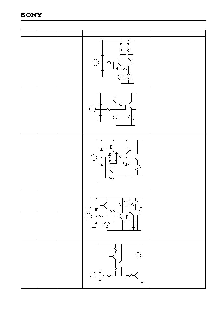
Trap connection.
Leave this pin open other than
when composite video input is
selected.
Outputs the video signal to be
input to the sync separation
circuit.
Composite video signal input
(Y signal when using Y/C input
and Y/color difference input).
The standard input level is 0.5
V
P-P
(from sync tip to 100 %
white).
IDENT detection filter con-
nection.
Leave this pin open other than
when PAL mode is selected.
Chroma signal input when
using Y/C input. Composite
video signal input is supported
when this pin is connected to
GND. Leave this pin open
when Y/color difference input.
The standard input level is
0.15 V
P-P
(burst).
GND
V
CC
1
V
EE
1
GND
V
CC
1
V
EE
2
GND
V
CC
1
V
EE
3
GND
V
CC
1
V
EE
4
GND
V
CC
1
V
EE
5
1
TRAP
2.0V
2
H FILTER
OUT
3
VIDEO IN
2.25V
4
IDENT
FILTER
5
C IN
2.5V
Pin No.
Symbol
Pin voltage
Equivalent circuit
Description
--4--
CXA1785AR
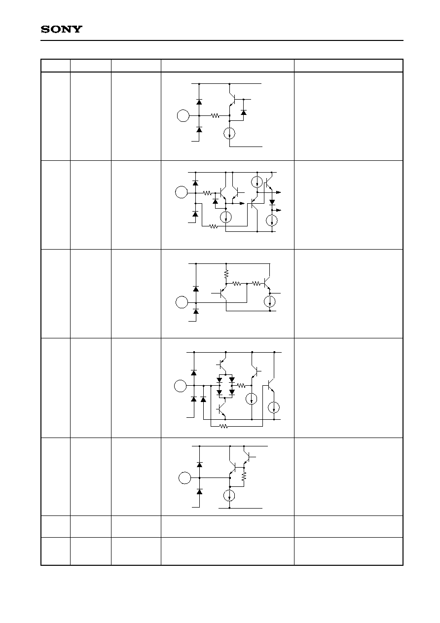
Color adjustment. The ampli-
tude of color difference signal
is adjusted when Y/color
difference input.
Burst cleaning coil is con-
nected for PAL.
Leave this pin open other than
when PAL mode is selected.
Killer detection filter is con-
nected.
Leave this pin open other than
when Y/color difference input
is selected.
Color difference demodulation
circuit inputs. Leave this pin
open for NTSC. Color
difference signal is input when
Y/color difference input.
In this case, input is pedestal
clamped by using external
coupling capacitor.
ACC detection filter is con-
nected.
Leave this pin open for Y/color
difference input.
GND
V
CC
1
V
EE
6
GND
V
CC
1
V
EE
7
GND
V
CC
1
V
EE
8
GND
V
CC
1
V
EE
9
10
V
CC
1
V
EE
11
6
COLOR
7
BURST
3.2V
OUT
8
KILLER
FILTER
9
R≠Y
1.9V
10
B≠Y
1.9V
11
ACC
FILTER
Pin No.
Symbol
Pin voltage
Equivalent circuit
Description
--5--
CXA1785AR
Color adjusted and burst taken
out chroma signal is output.
Color phase adjustment pin.
Also doubles as the NTSC,
PAL or Y/color difference
switch. PAL is selected when
this pin is connected to GND;
Y/color difference is selected
when this pin is connected to
Vcc1.
VXO input.
Leave this pin open for Y/color
difference input.
APC detection filter connection.
Leave this pin open for Y/color
difference input.
VXO output.
Leave this pin open for Y/color
difference input.
Ground.
Minimum electric potential con-
nection.
GND
V
CC
1
V
EE
12
GND
V
CC
1
V
EE
13
GND
V
CC
1
V
EE
14
GND
V
CC
1
V
EE
15
GND
V
CC
1
V
EE
16
12
CHROMA
2.3V
OUT
13
HUE
14
VXO IN
3.9V
15
APC
FILTER
16
VXO OUT
2.7V
17
GND
18
V
EE
Pin No.
Symbol
Pin voltage
Equivalent circuit
Description