 | –≠–ª–µ–∫—Ç—Ä–æ–Ω–Ω—ã–π –∫–æ–º–ø–æ–Ω–µ–Ω—Ç: CXA1797Q | –°–∫–∞—á–∞—Ç—å:  PDF PDF  ZIP ZIP |
--1--
E94X42-TE
Sony reserves the right to change products and specifications without prior notice. This information does not convey any license by
any implication or otherwise under any patents or other right. Application circuits shown, if any, are typical examples illustrating the
operation of the devices. Sony cannot assume responsibility for any problems arising out of the use of these circuits.
Absolute Maximum Ratings (Ta=25∞C)
∑ Supply voltage
V
CC
+12
V
(between V
CC
and V
EE
)
∑ Operating temperature Topr
≠20 to +75
∞C
∑ Storage temperature
Tstg
≠65 to +150
∞C
∑ Allowable power dissipation
P
D
1.02
W
Recommended Operating Conditions
Supply voltage
V
CC
±5.25 to ±6.0
V
Structure
Bipolar silicon monolithic IC
Description
The CXA1797Q is an audio signal processing LSI
designed for use in cassette decks.
Functions include Dolby B-C noise reduction,
recording equalizer amplifier, meter circuit
(logarithmic), bias control circuit, and playback
switching circuit. Serial control of these functions is
possible.
Features
∑ Few external parts
∑ Serial control of each functions possible
∑ Dolby B-C noise reduction
∑ Dolby S noise reduction select switch
∑ Recording equalizer amplifier
∑ Recording volume control
∑ Playback input select switch
∑ Meter circuit (logarithmic wave detection)
∑ Bias control circuit (left and right independent)
Applications
Cassette decks
Dolby B-C Type Noise Reduction System with Recording Equalizer Amplifier
64 pin QFP (Plastic)
CXA1797Q
This IC is available only to the licensees of Dolby Laboratories Licensing Corporation from whom licensing and applications
information may be obtained.
"Dolby" and the double D symbols are trade marks of Dolby Laboratories Licensing Corporation.
--2--
CXA1797Q
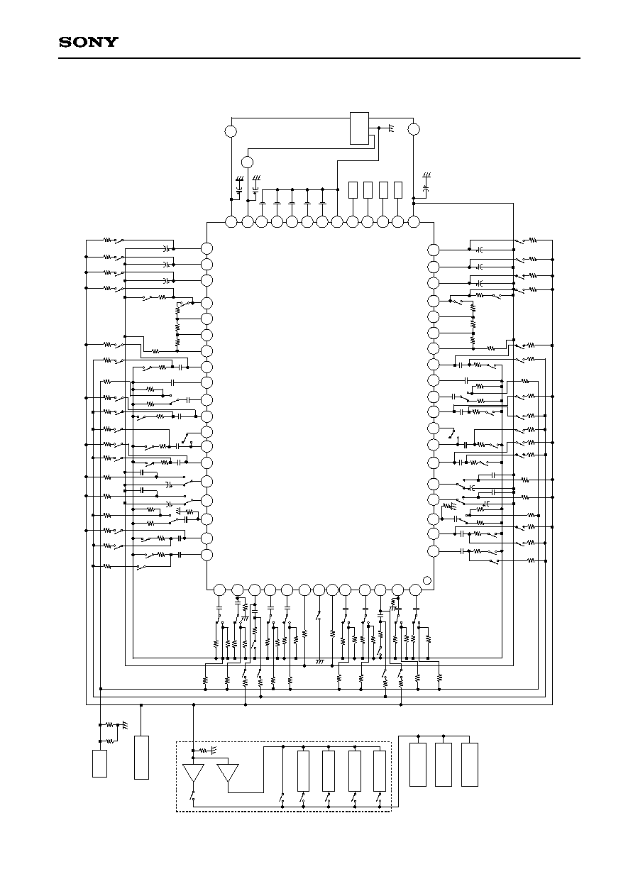
Block Diagram
C7
C8
0.1µ
0.068µ
R34
R53
76k
C17
BI
AS-M
BI
AS-C
BI
AS-N
R46
20k
Gm
3
R55
50k
RE
C O
U
T
-
4dB
v
RE
C CA
L
GH
C
A
L
FQ C
A
L
C11
R29
3.9k
L
I
N
E
IN
50k
R3
22k
2.
2µ
C2
R9
50k
6.
2k
L
-ch
R
-ch
GND
GN
D
R2
180k
C3
OS
C
TO L
I
N
E
IN
GN
D
-
6dB
v
10k
600
S
our
c
e
I
m
pedanc
e 10k
RV
A
VG
S
VG
S
Gm1
R11
6.
5k
GN
D
-
14dB
v
R13
3.3k
MPX
R17
-
26dB
v
R18
2k
C6
R16
40k
(C)
R22
40k
PB
(-6
d
Bm)
MO
A
OU
T
S I
N
RE
C/
P
B
f
o
r R
-ch
R1
GN
D
50k
R7
VG
S(C
)
R8
6.
5k
(C
)
(B)
VO
L
O
U
T
F
ilt
er
Dolby
RE
C I
N
VGS
-
26dB
v
(
-
25dB
m
)
RE
C
(
-
30dB
m
)
RE
C/
P
B
RE
C
R27
12k
R17
R21
22.
5k
(C)
VGS
R19
1.
5k
Do
lb
y
S-
N
R
(-6
d
Bm)
C9
(C)
VGS
(C
)
VG
S
-
23dB
v
R31
50k
RE
C
-
4
.
7dB
v
R37
R39
R38
2.8k
10.3k
Gm
2
Gm
5
◊
1
◊
1
Gm
4
◊
1
BPF
RE
A
22k
R57
R58
R59
R60
V
EE
MET
ER
O
U
T
to
M
E
T
E
R
IC
MET
ER
AC
L
I
N
E
OU
T
(
0dB
m
)
-
1dB
v
C13
1.0µ
GN
D
f
o
r R
-ch
GN
D
H
AED
PH
O
N
ES
F
r
om
LI
NE
O
U
T
Load I
m
pedanc
e 47k
ohm
10k
-
6dB
v
GN
D
VM
GN
D
C18
3.3µ
0dB
=
2
.
4
v
R54
150
V
EE
MET
AL
Cr
O
2
MET
AL
MET
AL
EQ
NO
RM
BI
AS O
U
T
50k
50k
50k
R63
R61
R56
DV
CC
GN
D
V
CC
Bi
a
s
PB
-EQ
PB
RE
C/
P
B
GN
D
C20
220p
L2
10m
H
C19
R62
10k
R
E
C
/
PB H
EAD
[
D
E
C
K-B ]
Bi
a
s
OS
C
(B)
VSG
R51
40k
-
8dB
v
C14
200p
(A)
GN
D
-
9
.
6dB
v
RE
C-
E
Q
I
N
R30
GND
C10
GND
-
10dB
v
L
I
N
E
IN
50k
R4
RE
C LE
V
E
L
BAL
AN
C
E
DA
T
A
CLK
LA
T
C
H
XR
ESET
V
CC
V
EE
G
N
D
(VG
)
R
E
C
/
PB I
R
EF
DV
CC
DG
ND
D
O
L
BY I
R
EF
V
EE
GN
D
R5
20k
R6
27k
GN
D
DV
CC
V
EE
V
EE
V
CC
PB I
N
1
-
21dB
v
PB I
N
2
-
21dB
v
2.
2µ
C1
PB O
n
l
y
[
D
E
C
K-A ]
GN
D
HE
A
D
BI
AS
CO
NT
RO
L
PR
E
-
21dB
v
A
DE
CK
DE
CK
A
/
B
B
DE
CK
R10
50k
VG
S
(C
)
-
21dB
v
PB O
U
T
R12
4.
7k
R15
10k
R14
22k
GN
D
GN
D
C4
390p
5.6m
H
L1
C5
2.2µ
(-3
0
d
Bm)
-
31dB
v
D
o
l
b
y PB I
N
Dolby
TC
1
Dolby
TC
2
V
EE
V
EE
SSK
H
L
S VF
LLS
V
F
AN
T
S
Dolby
B
/
C-
NR
-
7dB
v
(-6
d
Bm)
ME
T
E
R
(0
d
Bm)
-
1dB
v
R44
17k
R32
2.5k
VG
S
(C
)
7.
5k
G
a
in 12dB
up
R45
8.5k
DG
ND
DG
ND
100p
BVG
1.
25v
Do
l
b
y
-
NR
Do
l
b
y
-
NR
Do
l
b
y
-
NR
Do
l
b
y
-
NR
ME
T
E
R
P
B
-
DE
CK
L
I
NE
-
M
UT
E
T
ape-
E
Q
ME
T
A
L
SPEED
RE
C-
M
U
T
E
to
C
o
n
t
r
o
l
IC
PB -EQ
◊
1
-
10dB
v
BU
F
O
U
T
VG
S
(C
)
8.
2k
R28
(C)
VGS
+
6dB
v
R50
24k
(C)
VGS
G
ND (
A
)
C15
100p
GN
D
(A)
C16
100p
R49
8k
R47
20k
-
6dB
v
MT
R
HP Amp
R48
220
GN
D
GN
D
L
I
N
E
OU
T
R
-ch
L
-ch
f
o
r R
-ch
GND
7.
5k
R36
-
6dB
v
C12
4.7µ
R41
100k
10k
R43
4.
7k
R42
600
22k
130k
RE
C
LI
NE
VG
S
(B)
R35
8k
R33
8k
B/
C
N
R
BC
/
S
S-N
R
Dolby
RE
C O
U
T
R52
4k
C
A
L
I
BR
AT
I
O
N
-
1dB
v
22k
-1
0
dB
v
DV
CC
2.
2µ
2.2µ
2.2µ
2.2µ
0.
68µ
4.
7µ
10k
R40
10k
(C)
VGS
R20
1.
5k
R26
22.
5k
R25
12k
SSW
B/
C
NR
BC
/
S
S-N
R
SSW
(
-
6dB
m
)
PB
MO
A
R23
1.
5k
R24
1.
5k
VG
S
(C
)
PB
MO
A
(C)
VGS
RE
C/
P
B
RE
C
(C)
VGS
-
7dB
v
(-6
d
Bm)
PB
RE
C/
P
B
RE
C
O
FF/
O
N
B/
C
BC
/
S
RE
C/
P
B
NO
R/
CA
L
A/
B
O
FF/
O
N
120µ/
70µ
O
FF/
O
N
NO
RM
/
H
I
G
H
O
FF/
O
N
--3--
CXA1797Q
32
31
30
29
28
27
26
25
24
23
22
21
20
33
34
35
36
37
38
39
40
41
42
43
44
45
46
47
48
49
50
51
19
CONT
ME
T
E
R
2
ME
T
E
R
1
DO
L
B
Y
B
/
C NR
DO
L
B
Y
B
/
C NR
RE
C-
E
Q
BI
AS-
SW
18
17
16
15
14
13
12
11
10
9
8
7
6
5
4
3
2
1
52
53
54
55
56
57
58
59
60
61
62
63
64
BI
AS-
SW
RE
C-
E
Q
VO
L
U
M
E
VO
L
U
M
E
DE
CK
GN
D
C
X
A
1797Q
LI
NE
LM
UT
E
PB
CA
L
CA
L
ME
TER
OU
T1
B/C
TC
NR TC
BIAS1
OU
T
BIAS1
NO
RM
AL
BIAS1
CrO
2
BIAS1
ME
TA
L
REC E
Q O
UT
1
ME
TER
TC1
REC E
Q I
N1
REC O
UT
1
DO
LBY S I
N1
DO
LBY O
UT
1
LIN
E OU
T1
DO
LBY T
CL
1
DOL
BY
TCH1
REC I
N1
VO
LU
ME
OUT
1
BU
FFER
OU
T1
V
O
L
U
M
E
IN
1
D
O
L
BY PBI
N
1
PB O
U
T
1
PB I
N
B1
PB I
N
A1
D
O
L
BY I
R
EF
GN
D
R
E
C
/
PB I
R
EF
PB I
N
A2
PB I
N
B2
PB O
U
T
2
D
O
L
BY PBI
N
2
V
O
L
U
M
E
IN
2
V
CC
DV
CC
RE
C CA
L
FQ
C
A
L
GH
C
A
L
BAL
AN
C
E
R
E
C
L
EVEL
DG
ND
DA
T
A
CL
K
LA
T
C
H
XR
ESET
V
EE
ME
TER
OU
T2
S TC
RECM
UTE
TC
BIAS2
OU
T
BIAS2
NO
RM
AL
BIAS2
CrO
2
BIAS2
ME
TR
L
REC E
D O
UT
2
ME
TER
TC2
REC E
Q I
N2
REC O
UT
2
DO
LBY S I
N2
DO
LBY O
UT
2
LIN
E OU
T2
DO
LBY T
CL
2
DOL
BY
TCH2
REC I
N2
VO
LU
ME
OUT
2
BU
FFER
OU
T2
B/
C
S
B/
C
NM
DE
CK
LI
NE
LM
UT
E
VC5
RE
C
SPEED
ME
T
A
L
120µ/
70µ A
M
U
T
E
B/
C
NA
B/
C
SPEED
ME
T
A
L
120µ/
70µ A
M
U
T
E
MO
A
RE
C
RE
C
RE
C
MO
A
VCS
B
A
A
B
PB
PB
PB
PB
PB
S
Pin Configuration
--4--
CXA1797Q
Pin Description
(Ta = 25∞C, dual-power supply configuration, V
CC
= 5.5 V, V
EE
= 5.5 V, DV
CC
= 5.0 V)
Pin
Symbol
Typical pin voltage
I/O
Z (in)
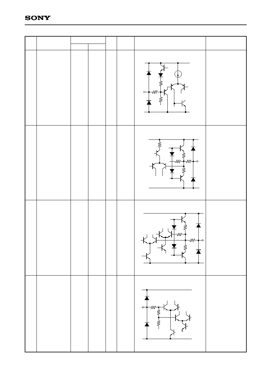
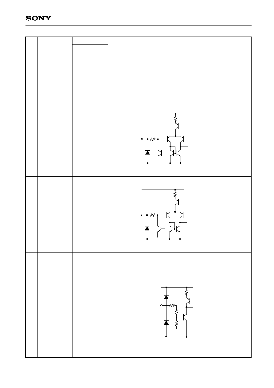
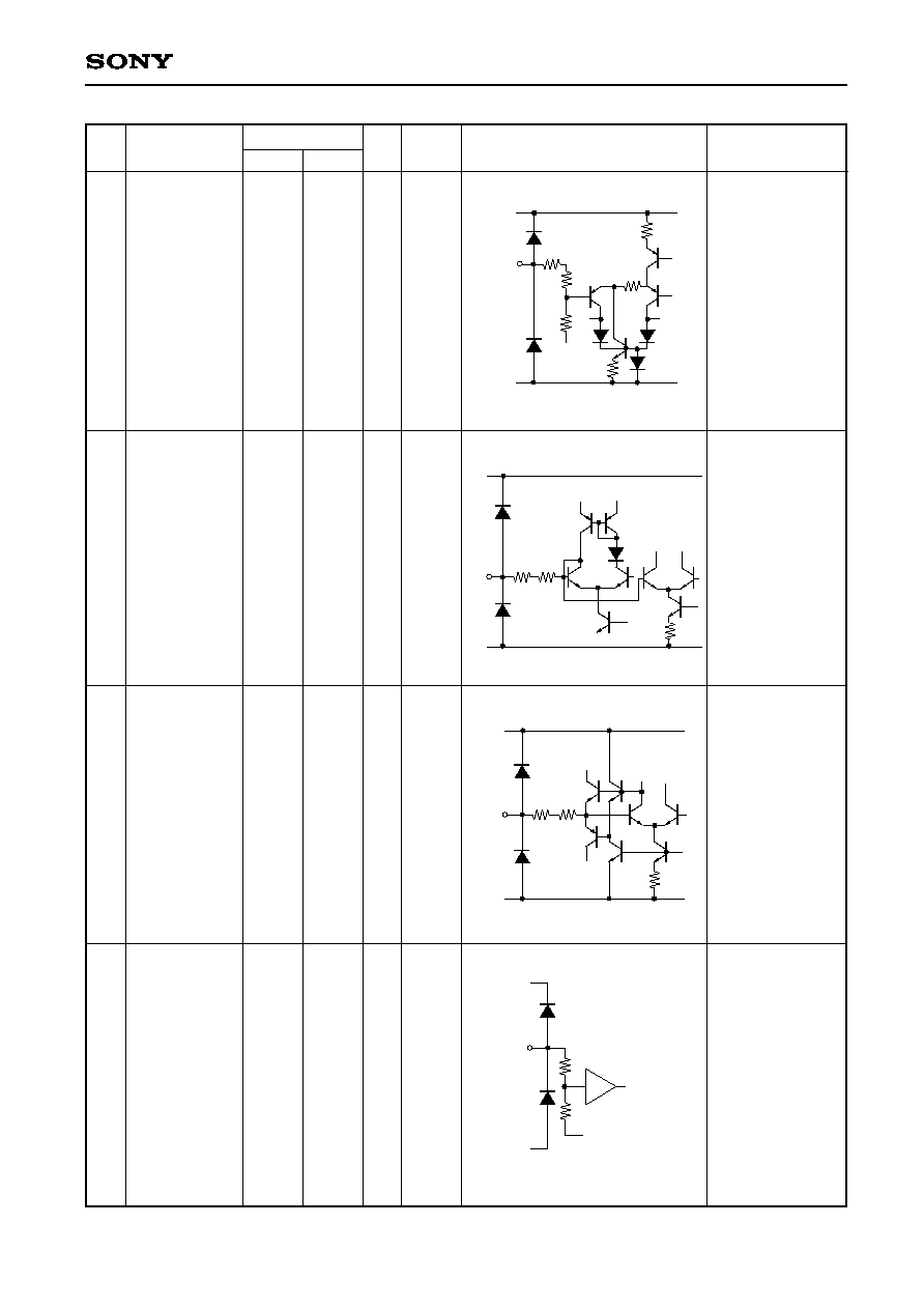
Equivalent circuit
Description
No.
DC
AC
Recording volume
input buffer output
Recording volume
output
Recording input
Time constant for
the HLS
V
CC
V
EE
6.5k
500
500
147
V
CC
V
EE
147
500
500
6.5k
147
V
CC
V
EE
40k
VCT
147
13k
36k
V
CC
V
EE
330k
1
51
2
50
3
49
4
48
BUFFER OUT1
BUFFER OUT2
VOLUME OUT1
VOLUME OUT2
REC IN1
REC IN2
DOLBY TCH 1
DOLBY TCH2
0.0V
0.0V
0.0V
V
EE
+0.4V
≠10dBv
≠10dBv
≠26dBv
(≠25dBm)
--
--
--
40k
--
O
O
I
--
--5--
CXA1797Q
Pin
Symbol
Typical pin voltage
I/O
Z (in)
Equivalent circuit
Description
No.
DC
AC
Time constant for
the LLS
Line output
Dolby S NR output
Dolby S NR input
V
CC
V
EE
147
13.5k
480k
8k
V
EE
300
300
147
V
CC
V
CC
V
EE
12k
147
200
200
147
22k
1.5k
VCT
V
CC
V
EE
5
47
6
46
7
45
8
44
DOLBY TCL1
DOLBY TCL2
LINE OUT1
LINE OUT2
DOLBY OUT1
DOLBY OUT2
DOLBY S IN1
DOLBY S IN2
V
EE
+0.9V
0.0V
0.0V
0.0V
--
≠1dBv
(0dBm)
≠7dBv
(≠6dBm)
≠7dBv
(≠6dBm)
--
--
--
23.5k
--
O
O
O

--6--
CXA1797Q
Pin
Symbol
Typical pin voltage
I/O
Z (in)
Equivalent circuit
Description
No.
DC
AC
Recording output
Recording
equalizer amplifier
input
DC cut
capacitance
Recording
equalizer amplifier
output
200
200
147
V
CC
V
EE
VCT
147
50k
V
CC
V
EE
300
300
8.5k
V
CC
V
EE
200
200
50k
147
V
CC
V
EE
9
43
10
42
11
41
12
40
REC OUT1
REC OUT2
REC EQ IN1
REC EQ IN2
METER AC1
METER AC2
REC EQ OUT1
REC EQ OUT2
0.0V
0.0V
0.0V
0.0V
≠7dBv
(≠6dBm)
≠23dBv
--
≠4dBV
--
50k
--
--
O
I
--
O

--7--
CXA1797Q
Pin
Symbol
Typical pin voltage
I/O
Z (in)
Equivalent circuit
Description
No.
DC
AC
Recording bias
control voltage
setting
Recording bias
control voltage
output
Time constant for
selecting NR mode
Time constant for
selecting B/C
mode
Time constant for
selecting S and
B/C modes
Meter output
(sensitivity:
65 mV/dB)
147
V
CC
V
EE
147
V
CC
V
EE
147
17k
V
CC
V
EE
DGND
4k
76.6k
100p
150
V
CC
V
EE
13
39
14
38
15
37
16
36
17
18
34
19
33
BIAS MTL1
BIAS MTL2
BIAS CrO
1
BIAS CrO
2
BIAS NORM1
BIAS NORM2
BIAS OUT1
BIAS OUT2
NR TC
B/C TC
S TC
METER OUT1
METER OUT2
V
EE
+1.25V
--
--
2.4V
--
--
--
--
--
--
17k
--
I
O
I/O
O
--8--
CXA1797Q
Pin
Symbol
Typical pin voltage
I/O
Z (in)
Equivalent circuit
Description
No.
DC
AC
Negative power
supply (Connect to
ground when using
a single power
supply)
Positive power
supply
Reset signal input
(active low)
Load signal input
Clock input
Data input
Logic and CAL
reference
Recording volume
adjustment
2.5V
DGND
reference
DGND
2k
V
CC
V
EE
2.5V
DGND
reference
DGND
4k
V
CC
V
EE
DGND
40k
147
60k
V
CC
V
EE
20
32
21
22
23
24
25
26
V
EE
V
CC
XRESET
LATCH
CLK
DATA
DGND
REC LEVEL
≠5.5V
+5.5V
--
--
0V
0V
--
--
--
--
--
--
--
--
--
100k
I
I
I
I
I
--9--
CXA1797Q
Pin
Symbol
Typical pin voltage
I/O
Z (in)
Equivalent circuit
Description
No.
DC
AC
Recording volume
balance
adjustment
High-frequency
gain adjustment of
recording
equalizer amplifier
Peak frequency Q
adjustment of
recording
equalizer amplifier
Recording
equalizer amplifier
gain adjustment
Logic power
supply
(DREF = 1/2
(DV
CC
+ DGND) is
CAL reference.)
DREF
70k
30k
147
V
CC
V
EE
147 54k
V
CC
V
EE
147 54k
V
CC
V
EE
DREF
DGND
30k
30k
DVCC
V
CC
V
EE
27
28
29
30
31
REC BALANCE
GH CAL
FQ CAL
REC CAL
DV
CC
2.5V
2.5V
2.5V
+5.0V
--
--
--
--
100k
54k
54k
--
I
I
I
I

--10--
CXA1797Q
Pin
Symbol
Typical pin voltage
I/O
Z (in)
Equivalent circuit
Description
No.
DC
AC
Time constant for
selecting
RECMUTE mode
Recording volume
input
Playback input
Head select output
of playback
equalizer amplifier
17k
147
V
CC
V
EE
50k
147
VCT
V
CC
V
EE
147
V
CC
V
EE
40k
VCT
300
147
300
V
CC
V
EE
35
52
64
53
63
54
62
RECMUTE TC
LINE IN2
LINE IN1
DOLBY PBIN2
DOLBY PBIN1
PBOUT2
PBOUT1
--
0.0V
0.0V
0.0V
--
≠10dBv
≠31dBv
(≠30dBm)
≠21dBv
17k
50k
40k
--
I/O
I
I
O

--11--
CXA1797Q
Pin
Symbol
Typical pin voltage
I/O
Z (in)
Equivalent circuit
Description
No.
DC
AC
Head select input
of playback
equalizer amplifier
Reference current
of recording
equalizer amplifier
Ground (center
capacitance when
using a single
power supply)
Reference current
VCT
50k
147
V
CC
V
EE
192
147
V
CC
V
EE
30k
30k
V
CC
V
EE
147
V
EE
+1.25V
V
CC
V
EE
55
56
60
61
57
58
59
PB IN B2
PB IN A2
PB IN A1
PB IN B1
REC IREF
GND
DOLBY IREF
0.0V
V
EE
+
1.25V
0V
V
EE
+
1.25V
≠21dBv
--
--
--
50k
--
--
--
I
--
--
--

--12--
CXA1797Q
Operating voltage range 1
(positive/negative dual power
supplies)
Operating voltage range 2
(single power supply)
Current consumption (ICC)
Recording equalizer amplifier
Recording reference output level
NORM-NORM mode
Recording equalizer amplifier
Recording reference input level
NORM-NORM mode
NORM-NORM mode
REC-EQ frequency response 1
(3 kHz, -20 dB)
NORM-NORM mode
REC-EQ frequency response 2
(8 kHz, -20 dB)
NORM-NORM mode
REC-EQ frequency response 3
(12 kHz, -20 dB)
CrO
2
-NORM mode
REC-EQ frequency response 1
(3 kHz, -20 dB)
CrO
2
-NORM mode
REC-EQ frequency response 2
(8 kHz, -20 dB)
CrO
2
-NORM mode
REC-EQ frequency response 3
(12 kHz, -20 dB)
METAL-NORM mode
REC-EQ frequency response 1
(3 kHz, -20 dB)
METAL-NORM mode
REC-EQ frequency response 2
(8 kHz, -20 dB)
METAL-NORM mode
REC-EQ frequency response 3
(12 kHz, -20 dB)
Entire LSI
Entire LSI
Entire LSI
Recording
equalizer amplifier
Recording
equalizer amplifier
Recording
equalizer amplifier
Recording
equalizer amplifier
Recording
equalizer amplifier
Recording
equalizer amplifier
Recording
equalizer amplifier
Recording
equalizer amplifier
Recording
equalizer amplifier
Recording
equalizer amplifier
Recording
equalizer amplifier
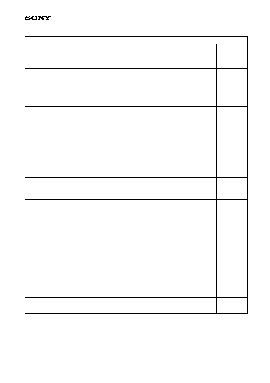
Electrical Characteristics Table
(Ta = 25∞C, dual-power supply configuration, V
CC
= 5.5 V, V
EE
= 5.5 V, DV
CC
= 5.0 V)
Block
Item
Conditions
Specifications
Unit
Min. Typ. Max.
No signal, no load, V
CC
= ± 5.5 V
Recording equalizer amplifier reference output level (315 Hz)
(This output level is the tape reference 0 dB which
generate magnetic flux of 250 nWb/m)
All of the recording equalizer amplifier blocks use this
level as their reference level.
Input level when the reference output level is 315 Hz,
-4 dBv
(For measurement, input a 315 Hz, -23 dBv signal to the
REC EQ IN pins and then measure the output level.)
NORM-tape, NORM-speed mode
Input a 3 kHz signal (-20 dB level down) to the REC EQ
IN pin and then measure the relative deviation from
NORM-NS, 315 Hz mode.
NORM-tape, NORM-speed mode
Input an 8 kHz signal (-20 dB level down) to the REC EQ
IN pin and then measure the relative deviation from
NORM-NS, 315 Hz mode.
NORM-tape, NORM-speed mode
Input a 12 kHz signal (-20 dB level down) from the
reference to the REC EQ IN pin and then measure the
relative deviation from NORM-NS, 315 Hz mode.
CrO
2
-tape, NORM-speed mode
Input a 3 kHz signal (-20 dB level down) to the REC EQ
IN pin and then measure the relative deviation from
NORM-NS, 315 Hz mode.
CrO
2
-tape, NORM-speed mode
Input an 8 kHz signal (-20 dB level down) to the REC EQ
IN pin and then measure the relative deviation from
NORM-NS, 315 Hz mode.
CrO
2
-tape, NORM-speed mode
Input a 12 kHz signal (-20 dB level down) to the REC EQ
IN pin and then measure the relative deviation from
NORM-NS, 315 Hz mode.
METAL-tape, NORM-speed mode
Input a 3 kHz signal (-20 dB level down) to the REC EQ
IN pin and then measure the relative deviation from
NORM-NS, 315 Hz mode.
METAL-tape, NORM-speed mode
Input an 8 kHz signal (-20 dB level down) to the REC EQ
IN pin and then measure the relative deviation from
NORM-NS, 315 Hz mode.
METAL-tape, NORM-speed mode
Input a 12 kHz signal (-20 dB level down) to the REC EQ
IN pin and then measure the relative deviation from
NORM-NS, 315 Hz mode.
±5.25 ±5.5 ±6.0
V
10.5 11.0 12.0
V
25.0 40.0 55.0
mA
--
≠4.0
--
dBv
≠24.5 ≠23.0 ≠21.5 dBv
≠1.7 ≠0.7 ≠0.3
dB
2.9
4.9
6.9
dB
7.8
10.8 13.8
dB
2.1
3.1
4.1
dB
4.5
6.5
8.5
dB
8.0
11.0 14.0
dB
3.7
4.7
5.7
dB
5.7
7.7
9.7
dB
8.4
11.4 14.4
dB

--13--
CXA1797Q
Recording
equalizer amplifier
Recording
equalizer amplifier
Recording
equalizer amplifier
Recording
equalizer amplifier
Recording
equalizer amplifier
Recording
equalizer amplifier
Recording
equalizer amplifier
Recording
equalizer amplifier
Recording
equalizer amplifier
Recording
equalizer amplifier
Recording
equalizer amplifier
Recording
equalizer amplifier
Recording
equalizer amplifier
Recording
equalizer amplifier
Block
Item
Conditions
Specifications
Unit
Min. Typ. Max.
NORM-HIGH mode
REC-EQ frequency response 1
(5 kHz, -20 dB)
NORM-HIGH mode
REC-EQ frequency response 2
(15 kHz, -20 dB)
NORM-HIGH mode
REC-EQ frequency response 3
(20 kHz, -20 dB)
CrO
2
-HIGH mode
REC-EQ frequency response 1
(5 kHz, -20 dB)
CrO
2
-HIGH mode
REC-EQ frequency response 2
(15 kHz, -20 dB)
CrO
2
-HIGH mode
REC-EQ frequency response 3
(20 kHz, -20 dB)
METAL-HIGH mode
REC-EQ frequency response 1
(5 kHz, -20 dB)
METAL-HIGH mode
REC-EQ frequency response 2
(15 kHz, -20 dB)
METAL-HIGH mode
REC-EQ frequency response 3
(20 kHz, -20 dB)
NORM-NORM mode
Channel crosstalk
(1 kHz, +12 dB, 1 kHz BPF)
NORM-NORM mode
REC-EQ signal handling
(1 kHz, THD = 1%, RL = 2.7 k
)
NORM-NORM mode
REC-EQ total harmonic distortion
(1 kHz, 0.0 dB, RL = 2.7 k
)
NORM-NORM mode
REC-EQ S/N ratio 1
("A"-WGT filter)
NORM-NORM mode
Output DC offset voltage
(REC OUT pin)
NORM-tape, HIGH-speed mode
Input a 5 kHz signal (-20 dB level down)to the REC EQ IN
pin and then measure the relative deviation from NORM-
NS, 315 Hz mode.
NORM-tape, HIGH-speed mode
Input a 15 kHz signal (-20 dB level down) to the REC EQ
IN pin and then measure the relative deviation from
NORM-NS, 315 Hz mode.
NORM-tape, HIGH-speed mode
Input a 20 kHz signal (-20 dB level down) to the REC EQ
IN pin and then measure the relative deviation from
NORM-NS, 315 Hz mode.
CrO
2
-tape, HIGH-speed mode
Input a 5 kHz signal (-20 dB level down) to the REC EQ
IN pin and then measure the relative deviation from
NORM-NS, 315 Hz mode.
CrO
2
-tape, HIGH-speed mode
Input a 15 kHz signal (-20 dB level down) to the REC EQ
IN pin and then measure the relative deviation from
NORM-NS, 315 Hz mode.
CrO
2
-tape, HIGH-speed mode
Input a 20 kHz signal (-20 dB level down) to the REC EQ
IN pin and then measure the relative deviation from
NORM-NS, 315 Hz mode.
METAL-tape, HIGH-speed mode
Input a 5 kHz signal (-20 dB level down) to the REC EQ
IN pin and then measure the relative deviation from
NORM-NS, 315 Hz mode.
METAL-tape, HIGH-speed mode
Input a 15 kHz signal (-20 dB level down) to the REC EQ
IN pin and then measure the relative deviation from
NORM-NS, 315 Hz mode.
METAL-tape, HIGH-speed mode
Input a 20 kHz signal (-20 dB level down) to the REC EQ
IN pin and then measure the relative deviation from
NORM-NS, 315 Hz mode.
NORM-tape, NORM-speed mode
Alternately input a 1 kHz signal (+12 dB level up) and
measure the channel crosstalk. (Use a 1 kHz BPF.)
NORM-tape, NORM-speed mode, RL = 2.7 k
Input a 1 kHz signal and set the output level so that THD
(total harmonic distortion) is 1%. (Measure the distortion
of a +9 dB level-up signal.)
NORM-tape, NORM-speed mode, RL = 2.7 k
Input a 1 kHz, 0 dB (reference input level) signal and
measure the distortion. (Measure the distortion as THD + N.)
NORM-tape, NORM-speed mode, Rg = 5.1 k
With no signal, measure the noise using the "A"-WGT
filter. (The measured value is indicated as the relative
value compared to the reference level.)
NORM-tape, NORM-speed mode
With no signal, measure the DC offset voltage of the REC
OUT pin.
≠6.2 ≠5.2 ≠4.2
dB
≠0.5
1.5
3.5
dB
3.0
6.0
9.0
dB
≠1.7 ≠0.7
0.3
dB
1.4
3.4
5.4
dB
4.1
7.1
10.1
dB
1.0
2.0
3.0
dB
2.1
4.1
6.1
dB
4.3
7.3
10.3
dB
--
≠90.0 ≠80.0
dB
9.0
11.0
--
dB
--
0.02
0.6
%
57.0 67.0
--
dB
≠0.5
0.0
0.5
V
--14--
CXA1797Q
Recording
equalizer amplifier
Recording
equalizer amplifier
Recording
equalizer amplifier
Recording
equalizer amplifier
Recording
equalizer amplifier
Recording
equalizer amplifier
Recording
equalizer amplifier
Recording
equalizer amplifier
Recording
equalizer amplifier
Recording volume
Recording volume
Recording volume
Recording volume
Recording volume
Block
Item
Conditions
Specifications
Unit
Min. Typ. Max.
NORM-NORM mode
REC-EQ mute characteristics
NORM-NORM mode
REC-EQ REC-CAL
characteristics 1
(REC-CAL = 5.0 V)
NORM-NORM mode
REC-EQ REC-CAL
characteristics 2
(REC-CAL = 0.0 V)
NORM-NORM mode
REC-EQ GH-CAL characteristics 1
(GH-CAL = 5.0 V)
NORM-NORM mode
REC-EQ GH-CAL characteristics 2
(GH-CAL = 0.0 V)
NORM-NORM mode
REC-EQ fQ-CAL characteristics
1-1
(fQ-CAL = 5.0 V)
NORM-NORM mode
REC-EQ fQ-CAL characteristics
1-2
(fQ-CAL = 5.0 V)
NORM-NORM mode
REC-EQ fQ-CAL characteristics
2-1
(fQ-CAL = 0.0 V)
NORM-NORM mode
REC-EQ fQ-CAL characteristics
2-2
(fQ-CAL = 0.0 V)
Recording volume amplifier
Recording volume characteristics 1
(REC-VOL = 5.0 V, REC-BAL =
2.5 V)
Recording volume amplifier
Recording volume characteristics 2
(REC-VOL = 2.0 V, REC-BAL =
2.5 V)
Recording volume amplifier
Recording volume attenuation
(REC-VOL = 0.0 V, REC-BAL =
2.5 V)
Recording volume amplifier
REC-VOL signal handling
(1 kHz, THD = 1%, RL = 2.7 k
)
Recording volume amplifier
REC-VOL total harmonic
distortion
(1 kHz, -10.0 dBv, RL = 2.7 k
)
NORM-tape, NORM-speed mode, REC-MUTE ON
Input a 1 kHz signal (+12 dB level up) and measure the
attenuation when REC MUTE is on. (Use a 1 kHz BPF.)
NORM-tape, NORM-speed mode, REC-CAL = 5.0 V
Input a 1 kHz signal (-20 dB level down) and measure the
amount of change compared to when the REC-CAL
function is at the standard setting.
NORM-tape, NORM-speed mode, REC-CAL = 0.0 V
Input a 1 kHz signal (-20 dB level down) and measure the
amount of change compared to when the REC-CAL
function is at the standard setting.
NORM-tape, NORM-speed mode, GH-CAL = 5.0 V
Input an 8 kHz signal (-20 dB level down) and measure
the amount of change compared to when the GH-CAL
function is at the standard setting.
NORM-tape, NORM-speed mode, GH-CAL = 0.0 V
Input an 8 kHz signal (-20 dB level down) and measure
the amount of change compared to when the GH-CAL
function is at the standard setting.
NORM-tape, NORM-speed mode, fQ-CAL = 5.0 V
Input an 8 kHz signal (-20 dB level down) and measure
the amount of change compared to when the fQ-CAL
function is at the standard setting.
NORM-tape, NORM-speed mode, fQ-CAL = 5.0 V
Input a 12 kHz signal (-20 dB level down) and measure
the amount of change compared to when the fQ-CAL
function is at the standard setting.
NORM-tape, NORM-speed mode, fQ-CAL = 0.0 V
Input an 8 kHz signal (-20 dB level down) and measure
the amount of change compared to when the fQ-CAL
function is at the standard setting.
NORM-tape, NORM-speed mode, fQ-CAL = 0.0 V
Input a 12 kHz signal (-20 dB level down) and measure
the amount of change compared to when the fQ-CAL
function is at the standard setting.
REC-VOL = 5.0 V, REC-BAL = 2.5 V
Input a 1 kHz, -10 dBv signal to the LINE IN pin and
measure the full gain of the recording volume amplifier.
REC-VOL = 2.0 V, REC-BAL = 2.5 V
Input a 1 kHz, -10 dBv signal to the LINE IN pin and
measure the attenuation of the recording volume
amplifier.
REC-VOL = 0.0 V, REC-BAL = 2.5 V
Input a 1 kHz, +2 dBv signal and measure the maximum
volume attenuation of the recording volume amplifier.
(Use a 1 kHz BPF.)
REC-VOL = 2.0 V, REC-BAL = 2.5 V, RL = 2.7 k
Input a 1 kHz signal and set the input level so that the THD is
1%. (Measure the distortion when the output is +2 dBv.)
REC-VOL = 2.0 V, REC-BAL = 2.5 V, RL = 2.7 k
Input a 1 kHz, -10 dBv signal (reference input level) and
measure the distortion. (Measure the distortion as THD +
N.)
--
≠88.0 ≠80.0
dB
4.6
6.1
7.6
dB
≠8.0 ≠6.5 ≠5.0
dB
0.7
2.2
3.7
dB
≠2.8 ≠1.3
0.2
dB
≠5.9 ≠4.4 ≠2.9
dB
≠8.4 ≠6.9 ≠5.4
dB
5.0
6.5
8.0
dB
4.9
6.4
7.9
dB
7.9
9.4
10.9
dB
≠10.2 ≠8.7 ≠7.2
dB
--
≠86.0 ≠80.0
dB
12.0 12.5
--
dB
--
0.15
0.5
%

--15--
CXA1797Q
Recording volume
Recording volume
Recording volume
Recording volume
Recording volume
Recording volume
Line amplifier
Line amplifier
Line amplifier
Line amplifier
Line amplifier
Line amplifier
Line amplifier
Level meter
Block
Item
Conditions
Specifications
Unit
Min. Typ. Max.
Recording volume amplifier
REC-VOL S/N ratio 1
("A"-WGT filter)
Recording volume amplifier
Output DC offset voltage
(VOL OUT pin)
Recording volume amplifier
REC-VOL balance
characteristics 1
(REC-VOL = 5.0 V, REC-BAL =
0.0 V)
Recording volume amplifier
REC-VOL balance
characteristics 2
(REC-VOL = 5.0 V, REC-BAL =
5.0 V)
Recording volume amplifier
Channel crosstalk
(REC-VOL = 5.0 V, REC BAL =
2.5 V)
Input buffer gain
(1 kHz, -10.0 dBv)
Line amplifier gain
(1 kHz, -30 dBm)
Line amplifier
Signal handling
(1 kHz, THD = 1%)
Line amplifier
Line amplifier total harmonic
distortion
(1 kHz, -30 dBm)
Line amplifier
Line amplifier S/N ratio
("A"-WGT filter)
Line amplifier
Output DC offset voltage
(LINE OUT pin)
Line amplifier
MUTE mode characteristics
(1 kHz BPF)
Line amplifier
Channel crosstalk
(1 kHz, -14.0 dBv, 1 kHz BPF)
Level meter amplifier
Level meter characteristics 1
(REC IN = 1 kHz, -26 dBv)
REC-VOL = 5.0 V, REC-BAL = 2.5 V
With no signal, measure the noise using an "A"-WGT
filter. (The measured value is indicated as the relative
value compared to the full-gain level.)
REC-VOL = 5.0 V, REC-BAL = 2.5 V
With no signal, measure the DC offset voltage of the VOL
OUT pin.
REC-VOL = 5.0 V, REC-BAL = 0.0 V (1 kHz BPF)
Input a 1 kHz, +2 dBv signal and measure the attenuation
of VOL OUT 1. (Input -10 dBv and confirm that there is no
attenuation at VOL OUT 2.)
REC-VOL = 5.0 V, REC-BAL = 5.0 V (1 kHz BPF)
Input -10 dBv and confirm that there is no attenuation at
VOL OUT 1. (Input a 1 kHz, +2 dBv signal and measure
the attenuation of VOL OUT 2.)
REC-VOL = 5.0 V, REC-BAL = 2.5 V
Alternately input a 1 kHz, +2 dBv signal, and measure the
channel crosstalk. (Use a 1 kHz BPF.)
Input a 1 kHz, -10 dBv signal to the LINE IN pin and
measure the gain at the BUF OUT pin.
PB mode
Input a 1 kHz, -30 dBm signal to the DOLBY PBIN pin
and measure the output level at the LINE OUT pins.
PB mode
Input a 1 kHz signal and set the output level so that the
THD is 1%.
PB mode
Input a 1 kHz, -30 dBm signal (reference input level) and
measure the distortion. (Measure the distortion as THD + N.)
PB mode
With no signal, measure the noise using an "A"-WGT
filter. (The measured value is indicated as the relative
value compared to the reference level.)
REC mode
With no signal, measure the DC offset voltage of the LINE
OUT pin.
PB, MUTE mode
Input a 1 kHz, -18 dBm signal to the DOLBY PB IN pin
and measure the attenuation when LINE MUTE is on.
(Use a 1 kHz BPF.)
PB mode
Alternately input a 1 kHz, -18 dBm signal to the DOLBY
PB IN pin and measure the channel crosstalk. (Use a 1
kHz BPF.)
METER ON, REC mode
Input a 1 kHz, -26 dBv signal to the REC IN pin and
measure the output DC voltage at the METER pin.
80.0 83.0
--
dB
≠0.15 0.0
0.15
V
--
≠96.0 ≠60.0
dB
≠1.0
0.0
1.0
dB
--
≠98.0 ≠80.0
dB
≠1.0
0.0
1.0
dB
≠1.0
0.0
1.0
dBm
12.0 12.6
--
dB
--
0.02
0.5
%
80.0 82.5
--
dB
≠0.2 ≠0.1
0.2
V
--
≠107.0 ≠80.0
dB
--
≠94.0 ≠80.0
dB
2.5
2.8
3.1
V

--16--
CXA1797Q
Level meter
Level meter
Level meter
Level meter
Level meter
Playback input
switch
Playback input
switch
Playback input
switch
Playback input
switch
Playback input
switch
Playback input
switch
BIAS SW
BIAS SW
BIAS SW
BIAS SW
Block
Item
Conditions
Specifications
Unit
Min. Typ. Max.
Level meter amplifier
Level meter characteristics 2
(REC IN = 1 kHz, -22 dBv)
Level meter amplifier
Level meter characteristics 3
(REC IN = 1 kHz, -36 dBv)
Level meter amplifier
Level meter characteristics 4
(REC IN = 1 kHz, -46 dBv)
Level meter amplifier
Level meter characteristics 5
(REC IN = no signal)
Level meter amplifier
Level meter CAL characteristics
(REC IN = 1 kHz, -58 dBv)
Playback input switch gain
(PB IN = 1 kHz, -21 dBv)
Playback input switch
Signal handling
(1 kHz, THD = 1%)
Playback input switch
Total harmonic distortion
(1 kHz, -21 dBv)
Playback input switch
S/N ratio
("A"-WGT filter)
Playback input switch
A/B DECK crosstalk
A-DECK mode
Playback input switch
Output DC offset voltage
(PB OUT pin)
Bias maximum output voltage
NORMAL mode
Bias output voltage 1
CrO
2
mode
Bias output voltage 2
METAL mode
Bias output voltage 3
METER ON, REC mode
Input a 1 kHz, -22 dBv (+4 dB level up) signal to the REC
IN pin and measure the output DC voltage at the METER
pin.
METER ON, REC mode
Input a 1 kHz, -36 dBv (-10 dB level down) signal to the
REC IN pin and measure the output DC voltage at the
METER pin.
METER ON, REC mode
Input a 1 kHz, -46 dBv (-20 dB level down) signal to the
REC IN pin and measure the output DC voltage at the
METER pin.
METER ON, REC mode
With no signal, measure the DC offset voltage at the
METER pin.
CAL ON, REC mode
Input a 1 kHz, -58 dBv (-32 dB level down) signal to the
REC IN pin and measure the output DC voltage at the
METER pin.
Input a 1 kHz, -21 dBv signal to the PB IN pin and
measure the level.
A-DECK mode
Input a 1 kHz signal to the PB IN1 pin and set the output
level so that the THD is 1%.
A-DECK mode
Input a 1 kHz, -10 dBv signal (input reference level) to the
PB IN1 pin and measure the distortion. (Measure the
distortion as THD + N.)
A-DECK mode
With no signal, measure the noise using the "A"-WGT
filter. (The measured value is indicated as the relative
value compared to the reference level.)
A-DECK mode
Input a 1 kHz, -9 dBv (+12 dB level up) signal to the B-
DECK side and measure the A/B-DECK crosstalk. (Use a
1 kHz BPF.)
A-DECK mode
With no signal, measure the DC offset voltage of the PB
OUT pin.
BIAS ON mode, RL = 4.7 k
Measure the output DC voltage of the BIAS OUT pin.
NORMAL mode
Set the external feedback resistance to 56 k
, 11 k
,
11 k
, and 11 k
, and measure the output DC voltage of
the BIAS OUT pin.
CrO
2
mode
Set the external feedback resistance to 56 k
, 11 k
,
11 k
, and 11 k
, and measure the output DC voltage of
the BIAS OUT pin.
METAL mode
Set the external feedback resistance to 56 k
, 11 k
,
11 k
, and 11 k
, and measure the output DC voltage of
the BIAS OUT pin.
2.75 3.05 3.35
V
1.85 2.15 2.45
V
1.2
1.5
1.8
V
--
0.01
0.1
V
1.2
1.5
1.8
V
≠22.0 ≠21.0 ≠20.0 dBv
12.0 30.0
--
dB
--
0.02
0.5
%
80.0 84.0
--
dB
--
≠89.0 ≠80.0
dB
≠0.2
0.0
0.2
V
4.8
5.0
--
V
≠2.4 ≠2.2 ≠2.0
V
≠0.75 ≠0.5 ≠0.25
V
4.2
4.5
4.8
V

--17--
CXA1797Q
DOLBY
DOLBY
DOLBY
DOLBY
DOLBY
DOLBY
DOLBY
DOLBY
DOLBY
DOLBY
DOLBY
DOLBY
DOLBY
DOLBY
DOLBY
DOLBY
DOLBY
Block
Item
Conditions
Specifications
Unit
Min. Typ. Max.
Dolby reference level
REC mode
REC IN level
PB mode
PB IN level
B type encoding
Boost characteristics 1
B type encoding
Boost characteristics 2
B type encoding
Boost characteristics 3
B type encoding
Boost characteristics 4
C type encoding
Boost characteristics 1
C type encoding
Boost characteristics 2
C type encoding
Boost characteristics 3
C type encoding
Boost characteristics 4
C type encoding
Boost characteristics 5
C type encoding
Boost characteristics 6
PB mode
Frequency response
REC mode
Signal handling
NR OFF total harmonic distortion
Dolby B total harmonic distortion
Value at the Dolby reference level of the REC OUT pin
REC mode, NR off, f = 1 kHz
Input a signal to the REC IN pin and measure the level at
which the level of the DOLBY OUT pin reaches -6 dBm.
PB mode, NR off, f = 1 kHz
Input a signal to the NR PB IN pin and measure the level
at which the level of the DOLBY OUT pin reaches
-6 dBm.
REC, Dolby B mode
Input a 500 Hz, -25 dB signal to the REC IN pin and
measure the boost at the REC OUT pin.
REC, Dolby B mode
Input a 5 kHz, -25 dB signal to the REC IN pin and
measure the boost at the REC OUT pin.
REC, Dolby B mode
Input a 10 kHz, -40 dB signal to the REC IN pin and
measure the boost at the REC OUT pin.
REC, Dolby B mode
Input a 10 kHz, 0 dB signal to the REC IN pin and
measure the boost at the REC OUT pin.
REC, Dolby C mode
Input a 500 Hz, -60 dB signal to the REC IN pin and
measure the boost at the REC OUT pin.
REC, Dolby C mode
Input a 500 Hz, -25 dB signal to the REC IN pin and
measure the boost at the REC OUT pin.
REC, Dolby C mode
Input a 2 kHz, -60 dB signal to the REC IN pin and
measure the boost at the REC OUT pin.
REC, Dolby C mode
Input a 2 kHz, -25 dB signal to the REC IN pin and
measure the boost at the REC OUT pin.
REC, Dolby C mode
Input a 5 kHz, -25 dB signal to the REC IN pin and
measure the boost at the REC OUT pin.
REC, Dolby C mode
Input a 10 kHz, 0 dB signal to the REC IN pin and
measure the boost at the REC OUT pin.
PB, Dolby off mode
Input a 20 kHz, -30 dBm signal to the NR PB IN pin and
measure the output at the REC OUT pin.
REC, NR off mode
Input a 1 kHz signal and set the output level so that the
THD is 1%. (Measure the distortion using a signal
boosted 13.5 dB from the reference.)
REC, NR off mode
Input a 1 kHz, +10 dB signal to the REC IN pin and measure
the distortion. (Measure the distortion as THD + N.)
REC, Dolby B mode
Input a 1 kHz, +10 dB signal to the REC IN pin and measure
the distortion. (Measure the distortion as THD + N.)
--
≠6.0
--
dBm
≠26.0 ≠25.0 ≠24.0 dBm
≠31.0 ≠30.0 ≠29.0 dBm
1.4
2.9
4.4
dB
3.9
5.4
6.9
dB
9.7
10.4 11.4
dB
≠1.1
0.4
1.9
dB
14.2 16.2 18.2
dB
7.2
9.2
11.2
dB
18.7 20.7 22.7
dB
5.4
7.4
9.4
dB
3.5
5.5
7.5
dB
≠5.5 ≠3.5 ≠1.5
dB
≠7.5 ≠6.0 ≠4.5 dBm
13.5 15.8
--
dB
--
0.02 0.15
%
--
0.04
0.2
%
--18--
CXA1797Q
DOLBY
DOLBY
DOLBY
DOLBY
DOLBY
DOLBY
DOLBY
DOLBY
Logic
Logic
Logic
Logic
Logic
Logic
Logic
Logic
Logic
Logic
Block
Item
Conditions
Specifications
Unit
Min. Typ. Max.
Dolby C total harmonic distortion
REC mode
Dolby C S/N ratio
PB mode
Recording
playback crosstalk
REC mode
Playback
recording crosstalk
REC mode
Channel crosstalk
PB mode
Channel crosstalk
REC mode
Output DC offset voltage 1
(REC OUT pin)
REC mode
Output DC offset voltage 2
(REC OUT pin)
High level input voltage
Low level input voltage
Clock frequency
Clock pulse width
Data setup time
Data hold time
Latch pulse width
Latch setup time
Latch hold time
Reset pulse width
REC, Dolby C mode
Input a 1 kHz, +10 dB signal to the REC IN pin and measure
the distortion. (Measure the distortion as THD + N.)
REC, Dolby C mode, Rg = 5.1 k
With no signal, measure the noise using the CCIR/ARM
filter. (The measured value is indicated as the relative
value compared to the DOLBY OUT level.)
PB, NR off mode
Input a 1 kHz, +10 dB signal to the REC IN pin and
measure the REC
PB crosstalk. (Use a 1 kHz BPF.)
REC, NR off mode
Input a 1 kHz, +10 dB signal to the NR PB IN pin and
measure the PB
REC crosstalk. (Use a 1 kHz BPF.)
PB, NR off mode
Input a 1 kHz, +10 dB signal to the REC IN pin and
measure the channel crosstalk. (Use a 1 kHz BPF.)
PB, NR off mode
Input a 1 kHz, +10 dB signal to the NR PB IN pin and
measure the channel crosstalk. (Ues a 1 kHz BPF.)
REC mode, NR off
B type
With no signal, measure the deviation in the output DC
offset voltage at the REC OUT pin when switching from
NR off mode to B type mode.
REC mode, NR off
C type
With no signal, measure the deviation in the output DC
offset voltage at the REC OUT pin when switching from
NR off mode to C type mode.
ViH
ViL
fck
tw
tsu(DATA
CLK)
tH(CLK
DATA)
tw(DATA)
ts(LATCH
DATA)
tH(CLK
LATCH)
tw(XRST)
--
0.08
0.3
%
60.0 61.0
--
dB
--
≠79
≠70
dB
--
≠90
≠70
dB
--
≠84
≠65
dB
--
≠85
≠65
dB
≠100
--
100
mV
≠100
--
100
mV
3.5
--
--
V
--
--
1.5
V
--
--
500
kHz
1
--
--
µs
1
--
--
µs
1
--
--
µs
1
--
--
µs
1
--
--
µs
1
--
--
µs
1
--
--
µs
--19--
CXA1797Q
5.
1k
S21
C26
S6
S1
0
R59
100
*R4
6
0dBm
R
25*
R
24*
10k
R100*
R101*
1.2k
O
s
c
illo
-
s
c
ope
Dis
t
o
r
t
io
n
A
n
a
l
yze
r
AC
Vo
l
t
m
e
t
e
r
CCI
R
1
k
H
z
BPF
DI
N A
u
d
i
o
"A
" W
T
G
Amp
30dB
Amp
0dB
GN
D
100k
F
i
l
t
er
m
odul
e
DC
Vo
l
t
m
e
t
e
r
A
udi
o
SG
1.2k
∑
0dB
m
=
.
7746V
r
m
s
f
o
r
D
o
l
b
y
∑
0dB
=
1
V
r
m
s
f
o
r
ot
her
t
e
s
t
s
S
501
GN
D
R
15*
10k
C14
R38
R55
S31
S29
0.1µ
-1dB
v
2.7k
0.068µ
R51
10k
C20
0.01µ
C22
10k
R50
C18
S28B
2.7k
R54
0.1µ
0.01µ
0.1µ
C28
R62
100
S35
*R8
0
R74
100
R84
10k
R86
R98
10k
R100
R102
R104
10k
R53
S28A
2.7k
100
S34
10k
C27
C31
0.1µ
R83
S53
4.7µ
C39
R99
R101
S57
C41
R103
C43
4.7µ
3.3µ
D2
4
D2
3
D2
2
D2
1
VO
L
U
ME I
N
2
D
O
L
BY PBI
N
2
PB O
U
T
2
PBI
N
B2
PBI
N
A2
PB I
R
EF
GN
D
D
O
L
BY I
R
EF
PB I
N
A1
PB I
N
B1
PB O
U
T
1
D
O
L
BY PBI
N
1
VO
L
U
ME I
N
1
V
CC
DV
CC
RQ
C CA
L
FQ C
A
L
GH
C
A
L
BAL
AN
C
E
R
E
C
L
EVEL
DG
ND
DA
T
A
CLK
LA
T
C
H
XR
ESET
V
EE
10k
S59
10k
10k
R95
3.3k
S52A
S55
R97
S50
56k
R7
9
11k
R9
1
11k
R8
9
11k
R87
10k
R85
10k
S48
100
S46
R77*
32.1k
0dBv
0.68µ
0.1µ
C37
2.7k
R81
S45A
C35
R79*
5.1k
C33
0.1µ
-6dB
m
-23dB
v
GND
GND
C4
7
10µ
C4
6
10µ
V30
0
V29
0
V28
0
V27
0
V26
0
DC A
m
m
e
t
e
r
V
CC
5V
V
EE
GN
D
DC A
m
m
e
t
e
r
DA
T
A
CL
K
LO
A
D
XR
ESET
R73*
100
S41
R71
10k
S39
S3
6
0.1µ
5.1k
R75
2.7k
R69
S38A
S33A
R57
100
R61
C25
R49
10k
0.1µ
C13
2.7k
R39
S19A
2.7k
-10dB
V
METER
OUT1
B/C
TC
NR TC
BIAS O
UT
1
BIAS C
rO
2
BIAS N
OR
MAL
BIAS MET
AL
REC E
Q O
UT
1
BOOS
T1
REC E
Q I
N1
DOLB
Y RE
C OU
T1
DO
LBY O
UT
1
LIN
E OU
T1
DO
LBY S I
N1
DO
LBY T
CL1
DO
LBY T
CH
1
REC I
N1
VOL
UMU
OU
T1
BU
FFER
OUT1
-21dB
V
C11
0.1µ
R35
S14
S14
R33
100
R37
S17
S20
R41
10k
100
R45*
75.9k
0dBm
S26
-25dB
m
0.1µ
C15
S24
C19
R47*
10k
C17
0.1µ
0.01µ
C21
C23
C4
5
10µ
GND
S52B
4.7µ
C42
R9
0
R88
S51
C44
4.7µ
3.3µ
S60
11k
3.3k
S45B
S49
R96
56k
11k
C40
10k
S58
10k
S56
S54
11k
R9
2
R9
4
S47
2.7k
R82
C38
0.1µ
C36
0.68µ
32k
*R7
8
R72
10k
100
5.1k
0.1µ
-23dB
v
C34
5.1k
*R7
6
0.1µ
C32
2.7k
R70
S388
S33B
R60
2.7k
R52
10k
C24
0.068µ
S25
S27
0.1µ
75.6k
10k
R42
100
R34
R36
S15
S15
C12
2.7k
0.1µ
0.1µ
R40
2.7k
S19B
-25dB
m
0.1µ
C16
S23
*R4
4
10k
*R4
8
S18
50k
S1
3
0.
1µ
-
10dB
V
-
30dB
m
S1
2
0.
1µ
-
10dB
V
0.
1µ
C1
5.
1k
R
13*
10k
0dB
v
R1
*
R
14*
R
22*
R
21*
R
20*
R
19*
R
17*
R
16*
R
23*
R
32*
5.
1k
R
31*
5.
1k
R
30*
10k
R
29*
2.
7k
R2
8
S5
B
C8
0.
1µ
-
21dB
V
0.
1µ
-
21dB
V
C6
0.
1µ
-
21dB
V
R
27*
R
26*
5.
1k
5.
1k
5.
1k
27k
S1
6
20k
5.
1k
5.
1k
5.
1k
R
18*
5.
1k
2.
7k
C4
C3
0.
1µ
0.
1µ
0.
1µ
0.
1µ
-
30dB
m
-
21dB
V
-
21dB
V
-
21dB
V
GND
S
502
S
503
S
504
S
505
S
506
∑
D
C
MEAS
∑
A
C
MEAS
∑A
C
I
N
∑V
EE
∑G
N
D
∑G
N
D
∑V
EE
∑A
C
I
N
∑
A
C
M
EAS
∑
DC M
E
A
S
33
34
35
36
37
38
39
40
41
42
43
44
45
46
47
48
49
50
51
-6dB
m
-6dB
m
12
52
53
54
55
56
57
58
59
60
61
62
63
64
29
28
27
26
25
24
23
22
21
20
32
31
30
DO
LBY S I
N2
DO
LBY O
UT
2
LIN
E OU
T2
BOOS
T2
RE
C E
Q IN
2
DOLB
Y RE
C OU
T1
REC E
Q O
UT
2
DOLB
Y T
CH2
DOLB
Y T
CH2
REC I
N2
VOL
UME O
UT
2
METER
OUT2
S TC
RECM
UTE
TC
BIAS2
OU
T
BIAS2
NO
MAL
BIAS2
CrO
2
BIAS2
METAL
BUF
FER
OU
T2
A
A
A
47k
S2
R4
100
138.
5k
R2
*
R3
10k
S1
0dB
v
R6
*
47k
R5
*
0dB
v
10k
S7
C2
S9
C5
S8
5.
1k
C1
0
C9
S1
1
C7
10k
R43*
S22
0.01µ
Po
w
e
r
S
uppl
y
DC A
m
m
e
t
e
r
19
18
17
16
15
14
13
11
10
9
8
7
6
5
4
3
2
1
-4dB
v
S43
10k
S5
A
0dB
m
47k
0dB
v
R7
*
47k
0dB
v
R7
*
S3
S4
R9
10k
R
12*
0dB
v
R
11*
138.
5k
R1
0
10k
0dB
100
S30
10k
S32
R58
R56
0dBv
0dBm
-4dB
v
S3
7
-6dB
m
0dB
V
100
C
X
A
1797Q
10k
10k
10k
10k
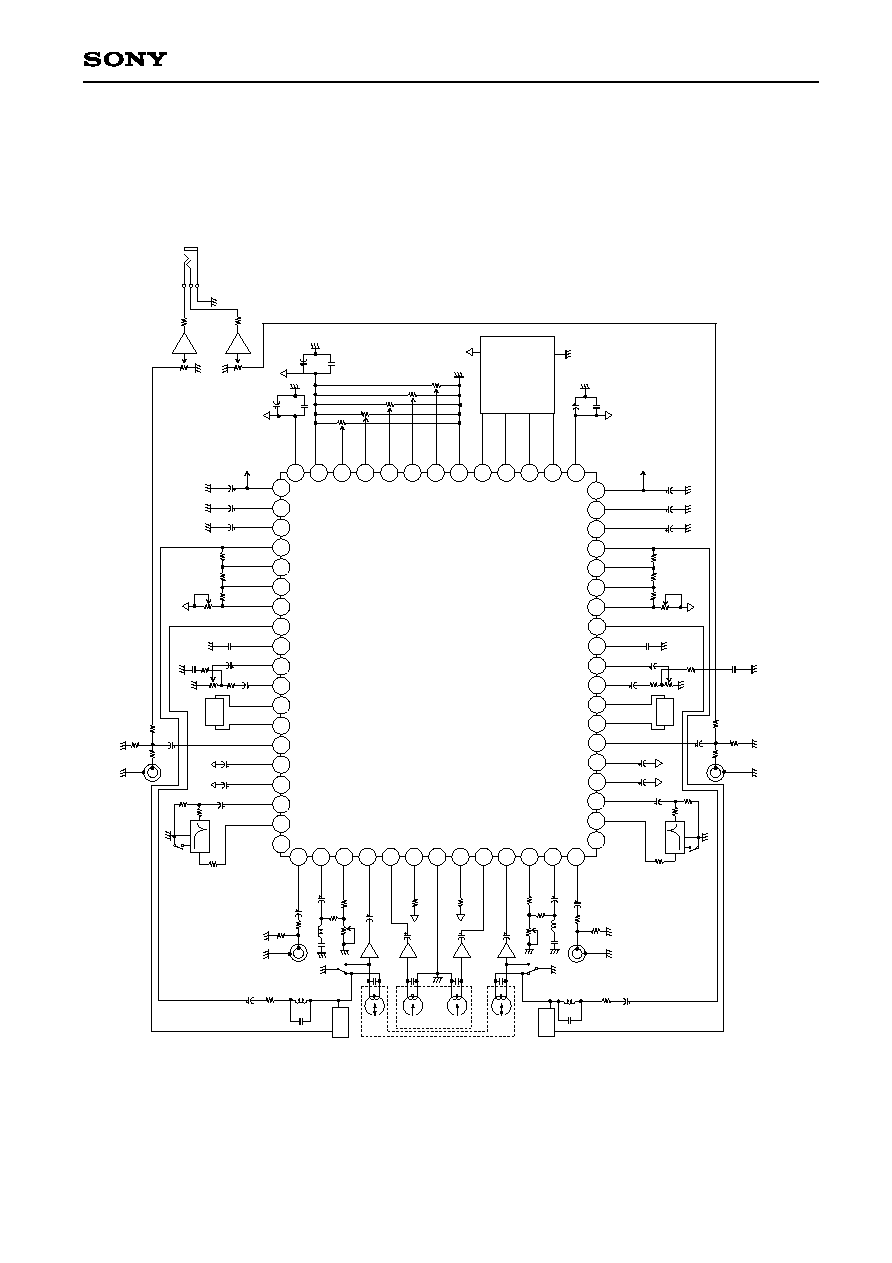
Electrical Characteristics Measurement Circuit
--20--
CXA1797Q
Application Circuit
GND
22k
R10
5.
6m
H
R42
50k
R41
50k
R40
50k
R39
50k
R38
50k
DGND
C35
0.
68µ
100µ
C34
V
EE
GND
REC/
PB
DO
LB
Y
PBI
N
2
P
B
OU
T2
PB I
N
B2
C8
B-L
PBEQ
2.
2µ
C6
PBEQ
2.
2µ
PB I
N
B1
B-R
22k
GND
DO
LB
Y
PBI
N
1
5.
6m
H
390p
GND
2.
2µ
C12
180k
R3
VO
L
U
ME
IN
1
R4
2.
2µ
C11
22k
GN
D
GN
D
GN
D
F
illt
er
MPX
3.3k
R14
-
14dB
v
R16
6.
2k
2k
R18
ON/OFF
-
26dB
v
C15
2.2µ
R22
R24
4.
7k
REC E
Q O
UT
1
DO
LBY S I
N1
DO
LBY O
UT
1
LIN
E OU
T1
DOLB
Y
TC
L1
REC
OUT1
RE
C E
Q IN
1
METE
R AC
1
2.2µ
C17
0.068µ
0.1µ
GN
D
8.2k
C23
R27
R26
C25
2.2µ
GN
D
1µ
C27
22k
R36
130k
R34
2.
2k
R32
600
22k
METER
OUT2
DO
LBY O
UT
2
R28
DOLB
Y T
CH2
DO
LBY T
CL2
220p
C2
100µ
C37
0.
68µ
C36
10k
C3
R1
4.7µ
64
63
62
61
60
59
58
57
56
55
54
53
52
20
21
22
23
24
25
26
27
28
30
31
32
51
50
49
48
47
46
45
44
43
42
41
40
39
38
37
36
35
34
33
1
2
3
4
5
6
7
8
9
10
11
12
13
14
15
16
29
H
AED
PH
O
N
ES
R46
220
HP
10k
GN
D
220
R45
GN
D
M i
c
ro
P
r
oc
es
s
r
DG
ND
C38
100µ
GND
C39
0.
68µ
DV
CC
GND
Amp
HP Amp
GN
D
GN
D
10k
R44
R43
BIASI
OU
T
BIASI
NO
RMAL
BIAS1
METAL
REC I
N1
VOL
UME
OUT1
BIAS1
CrO
2
BU
FFER
OUT1
METER
OU
T1
3.3µ
C33
19
to
M
E
T
E
R
IC
GN
D
4.7µ
C21
100k
GN
D
R20
7.
5k
DOLB
Y
TCH1
C19
GN
D
-
6dB
V
L
I
N
E
OU
T R
-
c
h
Dolby
S-N
R
4.7µ
C29
17
NR TC
4.7µ
C31
18
B/C
TC
S TC
RECM
UTE
TC
BIAS2
METAL
REC E
Q O
UT
2
METER
AC2
REC E
Q I
N2
DO
LBY S I
N2
LIN
E OU
T2
REC I
N2
VOL
UME O
UT
2
BU
FFER
OUT2
BIAS2
NO
RMAL
BIAS2
CrO
2
3.3µ
BIAS2
OU
T
REC
OUT2
VO
L
U
ME
IN
2
PB I
N
A2
R
E
Q IR
E
F
GN
D
PB I
N
A1
PB O
U
T
1
DO
LB
Y
I
R
EF
R13
C9
2.
2µ
L
I
N
E
IN
L
I
N
E
IN
REC/
PB
GN
D
GND
GN
D
GN
D
GN
D
C7
C8
OS
C
BI
AS
10mH
220p
C1
OS
C
BI
AS
C14
L2
10mH
10k
4.7µ
C4
R2
A-L
A-R
PBEQ
PBEQ
2.
2µ
390p
0.068µ
0.1µ
C18
2.2µ
C16
22k
C27
R21
R17
6.
2k
GN
D
ON/OFF
-
14dB
v
R15
3.3k
L
I
N
E
OU
T L
-
c
h
MPX
F
ilt
er
R19
2k
C20
GN
D
GN
D
R25
4.
7k
7.
5k
4.7µ
GN
D
GN
D
Dolby
S-N
R
C24
R29
4.7µ
C32
4.7µ
C30
R37
130k
R35
2.
2k
R33
600
R31
22k
C26
2.2µ
C28
1µ
to
M
E
T
E
R
IC
C
X
A
1797Q
180k
R4
22k
C13
2.
2µ
2.
2µ
10k
R12
L4
R11
4.
7k
R9
27k
R8
20k
R7
4.
7k
R6
L1
-
6dB
V
R23
100k
2.2µ
8.2k
C34
10k
R5
L3
R30
V
EE
V
EE
V
EE
V
EE
V
EE
V
EE
V
EE
V
EE
V
CC
DV
CC
RE
C CA
L
FQ C
A
L
GH
C
A
L
BAL
AN
C
E
RE
C
L
EVEL
DG
ND
DA
T
A
CLK
LA
T
C
H
XR
ESET
V
CC
DV
CC
V
EE
GN
D
GN
D
GN
D
3.9k
0.68µ
GN
D
0.68µ
3.9k
GN
D
GN
D
Application circuits shown are typical examples illustrating the operation of the devices. Sony cannot assume responsibility for
any problems arising out of the use of these circuits or for any infringement of third party patent and other right due to same.
--21--
CXA1797Q
Description of Operation
1. Logic Usage
The CXA1797Q is controlled by 11-bit serial data.
Note 1)
S mode takes precedence over other noise reduction modes. (When turning noise reduction off,
select BC mode.)
Note 2)
All data is initialized to "1" when a reset is executed.
2. Serial Data Format
An overview of the serial data format is shown below.
Note 3)
In this instance, have the LATCH signal rise while CLK is high.
D1
D2
D3
D4
D5
D6
D7
D8
D9
(Note 1)
D10
D11
Name
SPEED
METAL
EQ
A/B
METER
PB/REC
LMUTE
RMUTE
BC/S
B/C
NR ON/OFF
Function (DATA 1)
(Note 2)
NORM
METAL OFF
120µs
DECK A
METER GAIN NORM
PB MODE
LINE MUTE ON
REC MUTE ON
DOLBY NR B or C
DOLBY NR B
DOLBY NR OFF
Function (DATA 0)
HIGH
METAL ON
70µs
DECK B
METER GAIN HIGH (+12dB)
REC MODE
LINE MUTE OFF
REC MUTE OFF
DOLBY NR S
DOLBY NR C
DOLBY NR ON
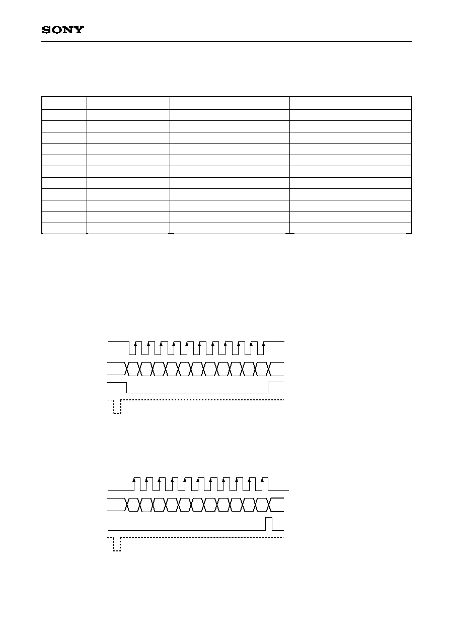
CLK
D1 D2 D3 D4 D5 D6 D7 D8 D9 D10 D11
DATA
LATCH
XRST
When using CLK and LATCH as normal high:
DATA is read at the
rising edge of CLK.
LATCH low : hold
LATCH high : load
Reset operation when low
(when reset is required)
CLK
D1 D2
D3 D4 D5
D6 D7 D8 D9 D10 D11
DATA
LATCH
XRST
When using CLK and LATCH as normal low
(Note 3)
:
DATA is read at the
rising edge of CLK.
LATCH low : hold
LATCH high : load
Reset operation when low
(when reset is required)

--22--
CXA1797Q
3. Timing Chart of 11-bit Serial Data Interface
t
SDK
CLK
DATA
LATCH
1.5V
3.5V
t
SLD
1.5V
t
HCD
t
WD
t
WC
t
WC
1.5V
3.5V
D1
D2
CLK
DATA
LATCH
1.5V
t
HCL
t
HLC
3.5V
D10
D11
t
WR
1.5V
XRESET
3.5V

--23--
CXA1797Q
4. Control pin usage
1) REC VOL
Connect a 50 k
variable resistor to this pin; this pin controls the electronic volume according to the
voltage (between DV
CC
and DGND) applied to this pin.
(Although other resistances and voltages can be used, the gain when the volume is at the center will
differ.)
2) REC BAL
This pin controls the electronic volume balance.
(Both channel sounds are output when voltage of (DV
CC
+ DGND)/2 is applied to this pin or when it is
open. When DV
CC
voltage is applied, only the CH1 sound is output, and when DGND voltage is
applied, only the CH2 sound is output.)
3) REC CAL
This pin adjusts the overall gain for the recording equalizer amplifier. (The gain is at the center when
voltage of (DV
CC
+ DGND)/2 is applied to this pin or when it is open.)
4) FQ CAL
This pin adjusts the high-frequency peak Q value for the recording equalizer amplifier. (FP and GP also
change.)
(The value is at the center when voltage of (DV
CC
+ DGND)/2 is applied to this pin or when it is open.)
5) GH CAL
This pin adjusts the middle/high frequency gain for the recording equalizer amplifier.
(The gain is at the center when voltage of (DV
CC
+ DGND)/2 is applied to this pin or when it is open.)
Low-frequency boost (external)
GH
Frequency (Hz)
RECCAL
GP/FP
FQ
Gain (dB)
--24--
CXA1797Q
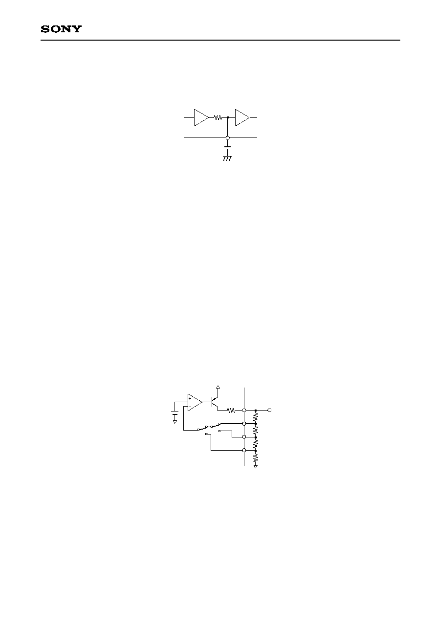
5. NR TC, BC TC, STC, RMUTE TC
These time constants are set in order to prevent the generation of a popping noise when one of the
switches operates. In addition, these functions can be controlled directly by applying voltage from an
external source. (In this case, the capability to drive 17 k
impedance is required.)
6. Meter circuit
The CXA1797Q meter circuit is a logarithmic detector.
The circuit has a sensitivity of 65 mV/dB and is designed to generate 2.8 V when the reference signal is
input.
This circuit has the temperature characteristics depend on Vt (= KT/q).
As a result, in order to satisfy the specifications, sufficient warmup time is required.
If METER GAIN is set to HIGH mode, the sensitivity is increased by 12 dB.
The METER AC pin is used to detect only the AC component, the low-frequency cut-off is determined by
the 8.5 k
internal resistance and the capacitance connected to this pin.
(With approximately 20 kHz at 1 µF, the high-frequency cut-off is fixed at 20 kHz.)
7. Bias circuit
This circuit generates the DC voltage that controls the bias oscillator.
The BIASOUT voltage is specified so that voltage equal to the internal reference voltage (V
EE
+ 1.25 V) is
generated at a pin selected according to the tape mode (BIAS N, BIAS C, or BIAS M).
The BIASOUT pin is provided with a protective resistor of 147
. Take into account the corresponding
voltage drop when the load current is high.
17k
147
NORM
METAL
CrO
2
V
EE
V
EE

--25--
CXA1797Q
Frequency (Hz)
≠10
0
10
20
30
10
100
1k
10k
100k
REC EQ frequency response
Output response (dB)
Vcc, V
EE
= ±5.5V
0dB = NORM Tape--NORM SPEED
315Hz, --24dBV
NORM--NORM
CrO
2
--NORM
METAL--NORM
NORM--HIGH
CrO
2
--HIGH
METAL--HIGH
REC EQ total harmonic distortion
Distortion (%)
Output level (dB)
10.0
1.0
0.1
≠12
≠8
≠4
0
4
8
12
V
CC
, V
EE
= ±5.5V
NORM Tape--NORM SPEED
0dB = --4dBV, RL = 2.7k
315Hz
1kHz
3kHz
6.3kHz
10kHz
15kHz
1k
100
10k
500
5k
Load resistance (
)
50k
100k
0
REC EQ load characteristics
Output level (dB)
2.0
4.0
6.0
8.0
10.0
12.0
14.0
V
CC
, V
EE
= ±5.5V
0dB = --4dBV
THD+N = 1%
NORM Tape--NORM SPEED
f=315Hz
f=1kHz

--26--
CXA1797Q
≠10
0
10
20
30
Output response (dB)
10
100
1k
10k
100k
Frequency (Hz)
REC CAL = 5.0V
REC CAL = 2.5V
REC CAL = 0V
REC CAL frequency response
10
100
10k
100k
≠10
0
10
20
30
Output response (dB)
GH CAL frequency response
GH = 0V
V
CC
, V
EE
= ±5.5V
NORM Tape--NORM SPEED
FQ CAL and GH CAL: open
0dB = 315Hz, --24dBV
Frequency (Hz)
V
CC
, V
EE
= ±5.5V
NORM Tape--NORM SPEED
REC CAL and FQ CAL: open
0dB = 315Hz, --24dBV
1k
GH = 2.5V
≠10
0
10
20
30
Output response (dB)
10
100
1k
10k
100k
Frequency (Hz)
FQ CAL = 2.5V
FQ CAL = 0V
FQ CAL = 5.0V
FQ CAL frequency response
GH = 5.0V
V
CC
, V
EE
= ±5.5V
NORM Tape--NORM SPEED
REC CAL and GH CAL: open
0dB = 315Hz, --24dBV

--27--
CXA1797Q
Output level vs. REC CAL voltage
Output level (dB)
REC CAL pin voltage (V)
≠6.0
≠4.0
≠2.0
0
2.0
4.0
6.0
0
1.0
2.0
3.0
4.0
5.0
V
CC
, V
EE
= ±5.5V
NORM Tape--NORM SPEED
GH CAL, FQ CAL = 2.5V
0dB = REC CAL, FQ CAL, GH CAL: open
--20dB (at 315Hz, --4dBv)
315Hz
3kHz
8kHz
12kHz
0
1.0
4.0
2.0
0
≠2.0
≠4.0
2.0
3.0
4.0
5.0
GH CAL pin voltage (V)
Output level vs. GH CAL voltage
Output level (dB)
315Hz
3kHz
8kHz
12kHz
8.0
6.0
4.0
2.0
0
0
1.0
2.0
3.0
4.0
5.0
≠2.0
≠4.0
≠8.0
FQ CAL pin voltage (V)
Output level (dB)
Output level vs. FQ CAL voltage
V
CC
, V
EE
=±5.5V
NORM Tape--NORM SPEED
REC CAL, GH CAL = 2.5V
0dB = REC CAL, FQ CAL, GH CAL: open
--20dB (at 315Hz, --4dBv)
315Hz
3kHz
8kHz
12kHz
V
CC
, V
EE
=±5.5V
NORM Tape--NORM SPEED
REC CAL, FQ CAL = 2.5V
0dB = REC CAL, FQ CAL, GH CAL: open
--20dB (at 315Hz, --4dBv)
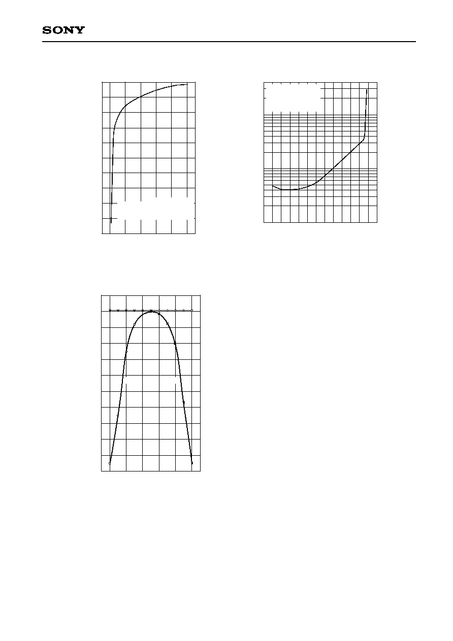
--28--
CXA1797Q
1.0
0.1
0.01
≠8
≠4
0
4
8
12
Output level (dB)
REC VOL total harmonic distortion
V
CC
, V
EE
= ±5.5V
REC LEVEL: 2.0V
0dB = ≠10dBV
f = 1kHz
Distortion (%)
REC LEVEL control voltage (V)
0
1.0
2.0
3.0
4.0
5.0
REC VOL gain (dB)
10
0
≠10
≠20
≠30
≠40
≠50
≠60
≠70
≠80
REC VOL gain vs. Control voltage
V
CC
, V
EE
= ±5.5V
NORM Tape-- NORM SPEED
Input: 1kHz, ≠10dBv
REC balance control voltage (V)
0
1.0
2.0
3.0
4.0
5.0
REC balance gain (dB)
10
0
≠10
≠20
≠30
≠40
≠50
≠60
≠70
≠80
≠90
≠100
1ch
2ch
REC balance characteristics
V
CC
, V
EE
= ±5.5V
NORM Tape--NORM SPEED
REC CAL, FQ CAL, GH CAL = 2.5V
0dB = REC LEVEL = 5.0V
BALANCE = 2.5V
Output for ≠10dBv input
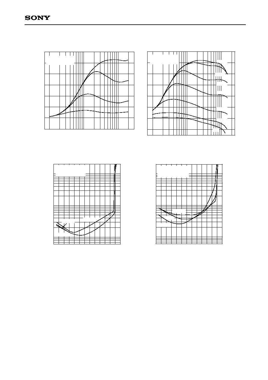
--29--
CXA1797Q
≠40dB
≠30dB
≠20dB
≠10dB
0dB
1k
100
10k
500
5k
Frequency (Hz)
≠2
Encoding boost (dB)
0
2
4
6
8
10
12
NR B type encoding characteristics
V
CC
, V
EE
= ±5.5V
0dB = Dolby Level
Frequency (Hz)
1k
100
10k
500
5k
200
2k
≠4
Encoding boost (dB)
0
4
8
12
16
20
≠30dB
≠20dB
≠10dB
0dB
≠60dB
≠50dB
≠40dB
NR C type encoding characteristics
V
CC
, V
EE
=± 5.5V
0dB = Dolby Level
Output level (dB)
4
8
Distortion (%)
0
≠4
0.01
0.02
0.05
0.1
0.2
0.5
1.0
2.0
12
16
18
f = 1kHz
f = 100Hz
f = 10kHz
NR off total harmonic distortion
V
CC
, V
EE
= ±5.5V
Encode Mode
0dB = Dolby Level
0.5
1.0
0.01
f=100Hz
≠4
0.02
0.05
0.1
0.2
2.0
0
4
8
12
16
18
Distortion (%)
NR B type total harmonic distortion
V
CC
, V
EE
= ±5.5V
Encode Mode
0dB = Dolby Level
f=10kHz
f=1kHz
Output level (dB)

--30--
CXA1797Q
≠4
0
4
8
12
16
Output level (dB)
NR C type total harmonic distortion
Distortion (%)
0.1
2.0
0.01
0.02
0.05
0.2
0.5
1.0
V
CC
, V
EE
= ±5.5V
Encode Mode
0dB = Dolby Level
f = 100Hz
f = 1kHz
1k
100
10k
500
5k
Frequency (Hz)
200
2k
≠60
Ripple elimination ratio (dB)
≠50
≠40
≠30
≠20
≠10
0
NR ripple rejection ratio 1
$
$
$ $ $ $
$
$
$
$
$
$
V
CC
Rejection on Split Supply
V
CC
, V
EE
=± 5.5V
NR off encoding mode
NR off decoding mode
NR B encoding mode
NR B decoding mode
NR C encoding mode
NR C decoding mode
$
1k
100
10k
500
5k
Frequency (Hz)
200
2k
≠60
NR ripple rejection ratio 2
Ripple rejection ratio (dB)
≠50
≠40
≠30
≠20
≠10
0
V
EE
Rejection on Split Supply
V
CC
, V
EE
= ±5.5V
NR off encoding mode
NR off decoding mode
NR B encoding mode
NR B decoding mode
NR C encoding mode
NR C decoding mode
$
$
$
$
$
$
$
$
$ $
$
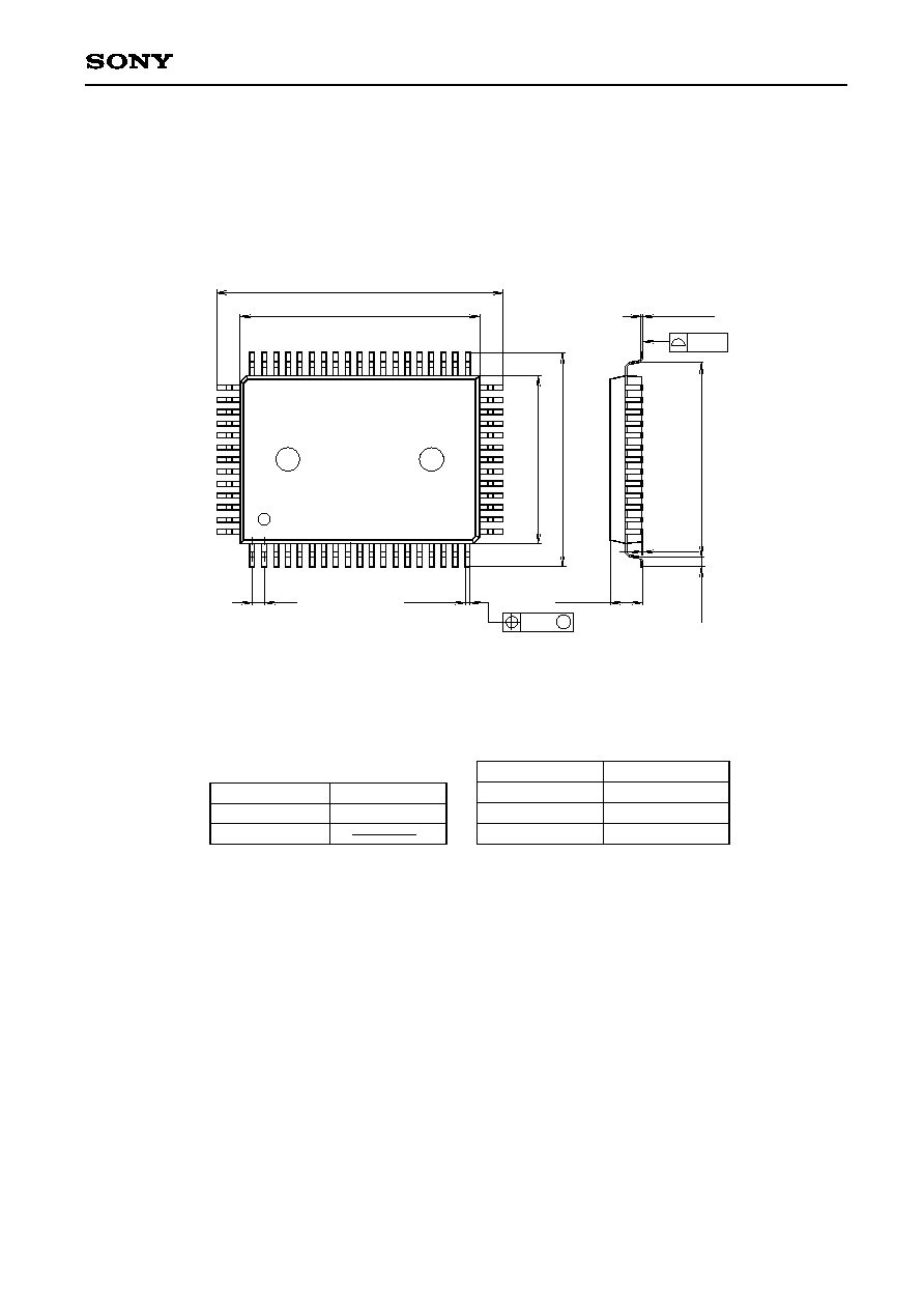
SONY CODE
EIAJ CODE
JEDEC CODE
23.9 ± 0.4
20.0 ≠ 0.1
1.0
0.4 ≠ 0.1
+ 0.15
14.
0
≠
0.
1
1
19
20
32
33
51
52
64
0.15 ≠ 0.05
+ 0.1
2.75 ≠ 0.15
16.
3
0.1 ≠ 0.05
+ 0.2
0.
8 ±
0.
2
M
± 0.12
0.15
+ 0.4
17.9 ±
0.4
+
0.
4
+ 0.35
64PIN QFP(PLASTIC)
QFP≠64P≠L01
QFP064≠P≠1420
PACKAGE MATERIAL
LEAD TREATMENT
LEAD MATERIAL
PACKAGE WEIGHT
EPOXY RESIN
SOLDER/PALLADIUM
COPPER /42 ALLOY
PACKAGE STRUCTURE
PLATING
1.5g
Package Outline Unit : mm
CXA1797Q
--31--