 | –≠–ª–µ–∫—Ç—Ä–æ–Ω–Ω—ã–π –∫–æ–º–ø–æ–Ω–µ–Ω—Ç: CXA1853Q | –°–∫–∞—á–∞—Ç—å:  PDF PDF  ZIP ZIP |

≠ 1 ≠
CXA1853Q
E95825-PP
RGB Driver for LCD
Description
The CXA1853Q is an RGB driver for LCD panels.
It supports a line alternative RGB drive system.
Features
∑ Built-in RGB signal phase matching sample-and-
hold circuit
∑ Effective frequency response (18MHz Typ.)
∑ Built-in gain and breakpoint variable 2-point
compensation circuit
∑ Built-in side black generation circuit for 4:3/16:9
aspect conversion
∑ Built-in VCOM voltage output circuit
Structure
Bipolar silicon monolithic IC
Applications
∑ Liquid crystal projectors
∑ Liquid crystal viewfinders
∑ Compact liquid crystal monitors
Absolute Maximum Ratings (Ta = 25∞C)
∑ Supply voltage
V
CC
1
6
V
V
CC
2
15
V
∑ Input pin voltage
V
IN
V
CC
1
V
∑ Operating temperature Topr
≠25 to +75
∞C
∑ Storage temperature
Tstg
≠55 to +150
∞C
∑ Allowable power dissipation
P
D
1500
mW
Operating Conditions
∑ Supply voltage
V
CC
1
4.75 to 5.25
V
V
CC
2
11.0 to 14.0
V
∑ RGB input signal voltage
V
IN
0.7
Vp-p
Note)
Note) Defined as the amplitude from the pedestal
level to white.
Sony reserves the right to change products and specifications without prior notice. This information does not convey any license by
any implication or otherwise under any patents or other right. Application circuits shown, if any, are typical examples illustrating the
operation of the devices. Sony cannot assume responsibility for any problems arising out of the use of these circuits.
80 pin QFP (Plastic)
For the availability of this product, please contact the sales office.

≠ 2 ≠
CXA1853Q
Block Diagram
70
69
68
67
63
64
65
66
61
62
71
72
73
74
75
76
77
78
79
80
21
22
23
24
25
26
27
28
29
30
40
39
38
37
36
35
34
31
32
33
2
3
4
5
6
7
8
9
10
11
12
13
14
15
16
17
18
19
20
1
R
CONT
B
CONT
AMP
AMP
AMP
CLP
CLP
CLP
BRT
CONT
BUFF
SW
BUFF
SW
BUFF
SW
BUFF
SW
SBRT
CONT
BUFF
PRG
SID
BUFF
BLKLMT
CTRL
GAIN
CONT
EA
S/H
S/H
S/H
S/H
S/H
GCA
S/H
S/H
CLP
RGB
CONT
SH1
TEST IN
PV
CC
GND
B CLAMP
G CLAMP
R CLAMP
RGB GAM GAIN1
R GAM GAIN1
B GAM GAIN1
RGB GAM GAIN2
R GAM GAIN2
B GAM GAIN2
RGB GAM CTR2
R GAM CTR2
B GAM CTR2
RGB GAM CTR1
R GAM CTR1
B GAM CTR1
N.C.
BLK CENT
VCOM OUT
BLK LIM
SIG CENT CTR
VCOM CTR
PRG
GND
SID FRP
FRP
PRG CTR
SID CTR
SID CLP
R CLP
G CLP
B CLP
R SBRT
B SBRT
RGB SBRT
GND
N.C.
N.C.
SH2
N.C.
SH3
SH4
GND
SIG SEL
GCA DETR
V
CC
4
IREF
GND
B GAIN
R GAIN
RGB GAIN
XCLP2
TEST SEL
WHT LIM
GCA DETG
GCA DETB
XCLP1
RGB MBRT
N.C.
N.C.
R MBRT
TEST OUT
V
CC
1
GND
SID OUT
V
CC
2
R OUT
G OUT
N.C.
BIN
B OUT
B MBRT
N.C.
GIN
RIN
V
CC
3
N.C.
S/H
S/H
41
42
43
44
45
46
47
48
49
50
51
52
53
54
55
56
57
58
59
60
EA
EA
GCA
GCA
≠ 3 ≠
CXA1853Q
Pin Description
(V
CC
1 = 5V, V
CC
2 = 13V)
Pin
NO.
Symbol
Pin voltage
Equivalent circuit
Description
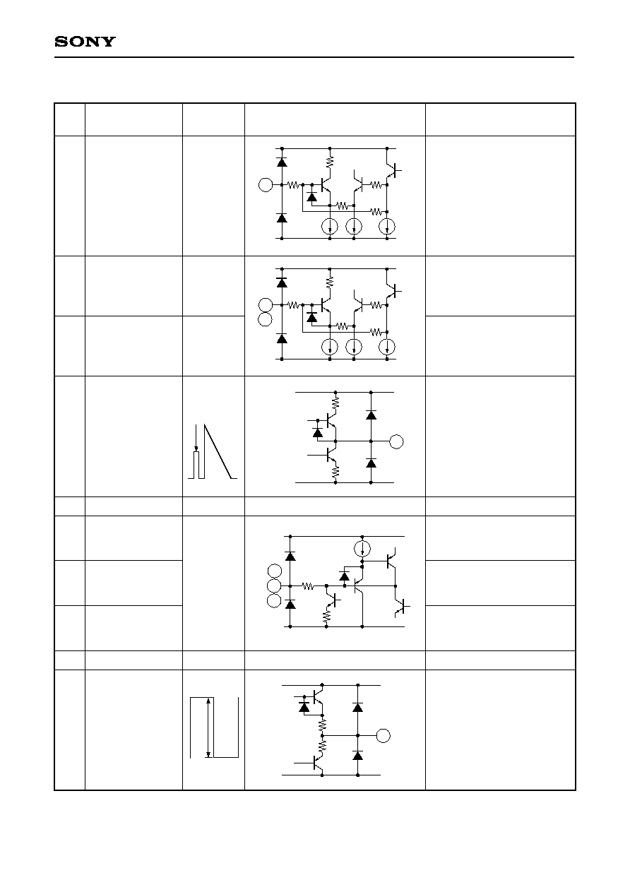
1
RGB MBRT
1.6 to 5.0V
RGB signal common main
brightness control. Preset
internally to 3.3V.
4
R MBRT
1.6 to 5.0V
R signal main brightness
control. Preset internally to
3.3V.
5
B MBRT
1.6 to 5.0V
B signal main brightness
control. Preset internally to
3.3V.
7
TEST OUT
2V
Measurement output.
This pin should be left open.
8
V
CC
1
5V
5V power supply.
9
RIN
0V
R signal input.
Input a 0.7Vp-p signal.
Note 2)
10
GIN
G signal input.
Input a 0.7Vp-p signal.
Note 2)
11
BIN
B signal input.
Input a 0.7Vp-p signal.
Note 2)
12
GND
GND.
13
SID OUT
SID signal output.
1
V
CC
1
GND
80k
80k
37k
200
40µA
40µA
40µA
2k
V
CC
1
GND
80k
80k
74k
200
20µA
40µA
20µA
4
5
5k
V
CC
1
GND
100
7
100
10
11
V
CC
1
GND
200
50µA
6.2k
9
V
CC
2
GND
10
13
10
Note 1)
in the Pin voltage indicates external applied voltage.
Note 2) Defined as the amplitude from the pedestal level to white.
Reference level
9.3Vp-p
Typ.
≠ 4 ≠
CXA1853Q
14
V
CC
2
13V
5V
13V power supply.
15
R OUT
R signal output.
16
G OUT
G signal output.
17
B OUT
B signal output.
18
V
CC
3
5V power supply.
0V
22
GND
GND.
1.6 to 5.0V
23
RGB SBRT
RGB signal common sub
brightness control.
1.6 to 5.0V
24
B SBRT
B signal sub brightness
control.
Preset internally to 3.3V.
1.6 to 5.0V
4.7 to 8.3V
25
R SBRT
R signal sub brightness
control.
Preset internally to 3.3V.
26
B CLP
B output detection signal
input.
27
G CLP
G output detection signal
input.
28
R CLP
R output detection signal
input.
Note)
in the Pin voltage indicates external applied voltage.
4.5V
Typ.
15
16
17
V
CC
2
GND
10
10
V
CC
3
GND
200
27k
200
53µA
13µA
53µA
3k
23
V
CC
3
GND
80k
80k
118k
200
26µA
40µA
26µA
3k
24
25
V
CC
2
GND
2k
200
10µA
26
27
28
Pin
NO.
Symbol
Pin voltage
Equivalent circuit
Description
≠ 5 ≠
CXA1853Q
29
SID CLP
4.7 to 8.3V
SID output detection signal
input.
Use an average value
detecting external capacitor
with a small leak current
absolute value and
tolerance.
29
V
CC
2
GND
2k
200
10µA
30
SID CTR
1.6 to 5.0V
SID output amplitude control.
Preset internally to 3.3V.
30
V
CC
3
GND
80k
80k
35k
200
53µA
40µA
53µA
3k
31
PRG CTR
1.6 to 5.0V
0V
Level control for the PRG
signal inserted into the SID
signal.
31
V
CC
3
GND
200
3k
90k
90k
32
FRP
FRP input. This pulse is
used to invert the polarity of
the RGB output. Output is
inverted when Low, and non-
inverted when High.
Input level: High
4V
Low
1V
V
CC
3
GND
200
32
10µA
33
SID FRP
FRP pulse input for SID
output. This pulse is used to
invert the polarity of the SID
output. Output is inverted
when Low, and non-inverted
when High.
Input level: High
4V
Low
1V
34
GND
GND.
33
V
CC
3
GND
200
10µA
Note)
in the Pin voltage indicates external applied voltage.
5V
0V
5V
0V
Pin
NO.
Symbol
Pin voltage
Equivalent circuit
Description