 | –≠–ª–µ–∫—Ç—Ä–æ–Ω–Ω—ã–π –∫–æ–º–ø–æ–Ω–µ–Ω—Ç: CXA1911 | –°–∫–∞—á–∞—Ç—å:  PDF PDF  ZIP ZIP |

--1--
E93Y13-TE
Absolute Maximum Ratings (Ta=25∞C)
∑ Supply voltage
V
CC
12
V
∑ Operating temperature Topr
≠40 to +85
∞C
∑ Storage temperature
Tstg
≠65 to +150
∞C
∑ Allowable power dissipation
P
D
430
mW
Recommended Operating Conditions
∑ Supply voltage
V
CC
7.8 to 11
V
Description
The CXA1911Q is an IC designed for use in car
stereo cassette decks. Functions include Dolby B/C
type noise reduction, playback equalizer amplifier
and music sensor into a single chip.
Features
∑ Few external parts
∑ Forward/Reverse head switching
∑ Small package (40-pin QFP)
∑ Dolby B/C type noise reduction and playback
equalizer into a single chip
∑ Same pin configuration as Dolby B type noise
reduction system (CXA1910Q)
∑ Music sense level can be set by external
resistors/capacitors (2 modes).
∑ High-band cut filter frequency can be adjusted by
the external capacitance.
Applications
∑ Car stereo cassette decks
∑ Cassette decks (playback only)
Structure
Bipolar silicon monolithic IC
Dolby B/C Type Noise Reduction System with Playback Equalizer
40 pin QFP (Plastic)
CXA1911Q
These ICs are available only to the licensees of Dolby Laboratories Licensing Corporation from whom licensing and applications
information may be obtained.
"Dolby" and the double D symbols are trade marks of Dolby Laboratories Licensing Corporation.
Sony reserves the right to change products and specifications without prior notice. This information does not convey any license
by any implication or otherwise under any patents or other right. Application circuits shown, if any, are typical examples
illustrating the operation of the devices. Sony cannot assume responsibility for any problems arising out of the use of these
circuits.
For the availability of this product, please contact the sales office.
--2--
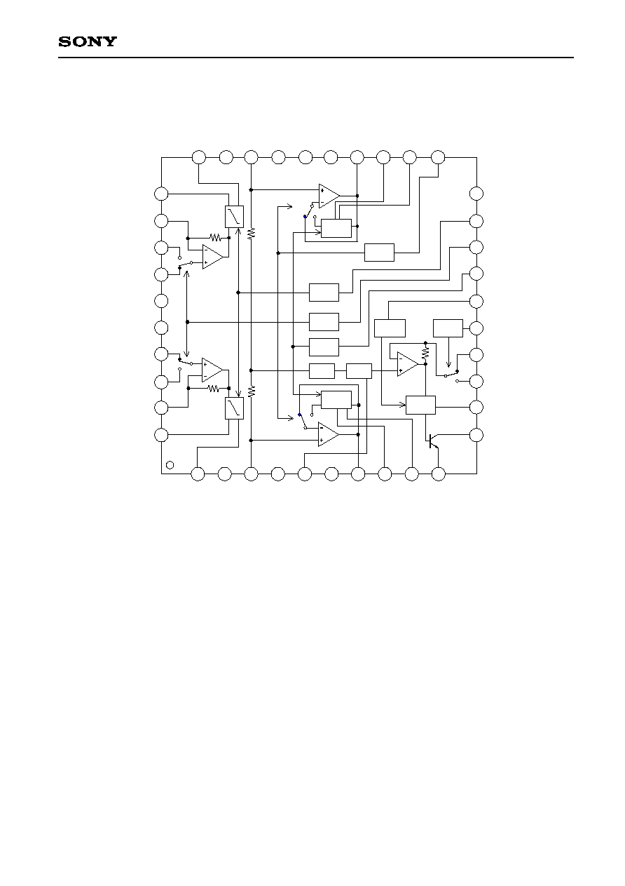
CXA1911Q
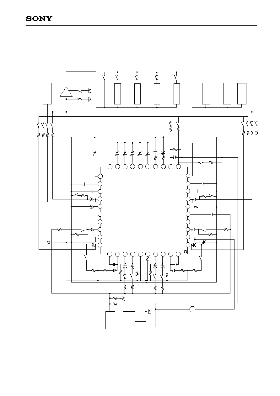
Block Diagram
NC
TAPESW
DRSW
NRMODE
MSSW
MSMODE
G1 (FF)
G2 (NOR)
MSTC
MSOUT
MS
G
N
D
T
CH2
TC
L
2
LI
N
E
O
U
T
2
D I
R
E
F
MS
L
P
F
NC
T
APEI
N
2
Vc
c
PBO
U
T
2
NRS
W
T
CH1
TC
L
1
LI
N
E
O
U
T
1
VC
T
NC
NC
T
APEI
N
1
GN
D
PBO
U
T
1
PBTC1
PBFB1
PBRIN1
PBFIN1
PBGND
E IREF
PBFIN2
PBRIN2
PBFB2
PBTC2
300k
300k
10dB
LPF
DET
A MS
MODE
NR
DR
TA PE
IN
G1/G2
22
21
23
24
25
26
27
28
29
30
20
19
18
17
16
15
14
13
12
1
2
3
4
5
6
7
8
9
10
11
31
32
33
34
35
36
37
38
39
40
F/R
F/R
NR
NR
--3--
CXA1911Q
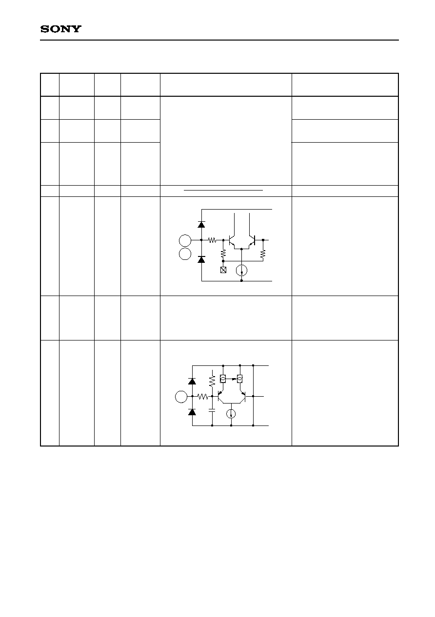
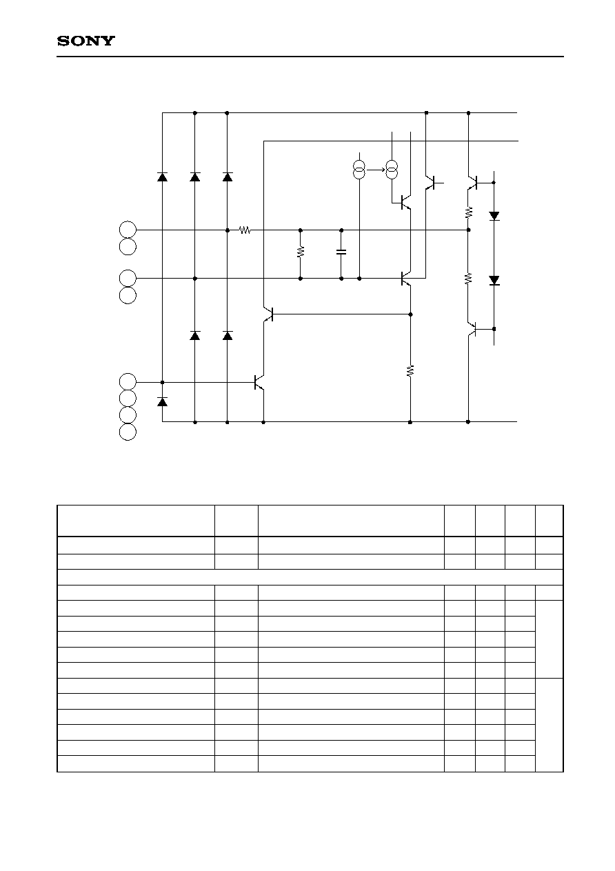
Pin
Symbol
DC
Z (in)
Equivalent circuit
Description
No.
value
Refer to Page 7.
147
V
CC
GND
100k
5
64p
12µA
147
VGS
28
3
40k
1
PBOUT
2.1V
--
30
32
PBFB
2.1V
300k
39
33
PBIN
0V
--
34
37
38
2
V
CC
8.0V
--
3
TAPEIN
4.0V
40k
28
4
NC
--
--
20
26
27
5
MSLPF
4.0
100k
PBEQ output
PBEQ feedback
PBEQ input
Power supply
TAPE input
No connection
Adjustment of MS LPF
frequency
Pin Description
(Ta=25∞C, V
CC
=8.0V, no signal)
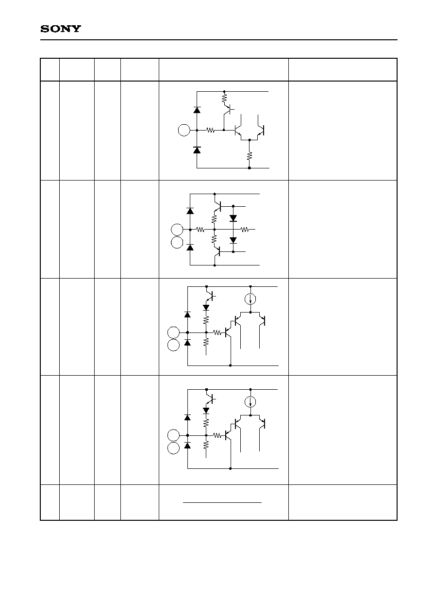
--4--
CXA1911Q
Pin
Symbol
DC
Z (in)
Equivalent circuit
Description
No.
value
6
D IREF
1.25V
--
7
LINEOUT
4.0V
--
24
8
TCL
0.3V
--
23
9
TCH
0.3V
--
22
10
MSGND
0.0V
--
29
GND
35
PBGND
Connection of reference
current setting resistor for
Dolby block
Line output
Time Constant pin for the LLS
Time Constant pin for the HLS
Ground
480k
23
8
147
13.5k
330k
22
9
147
36k
147
50k
6
147
V
CC
GND
200
200
7
24
--5--
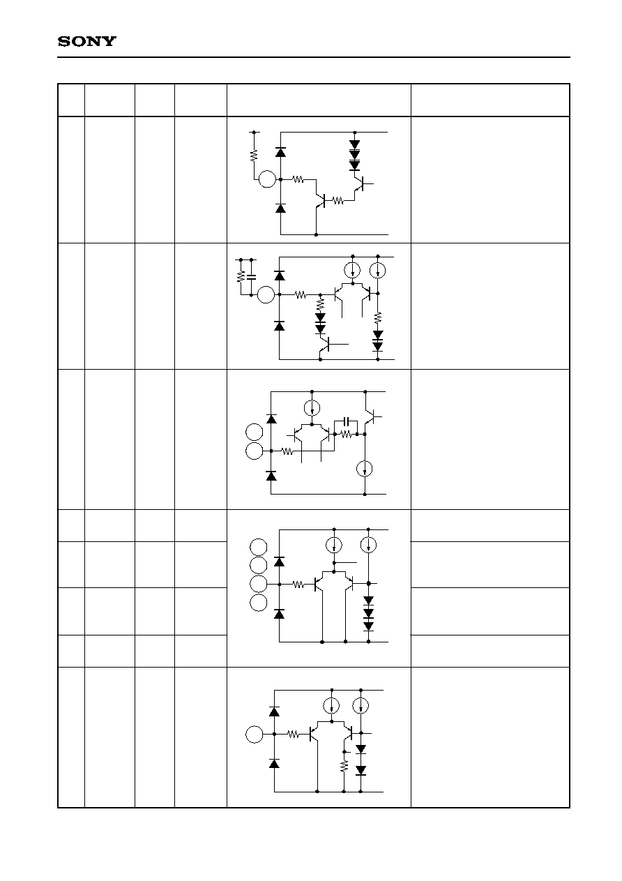
CXA1911Q
Pin
Symbol
DC
Z (in)
Equivalent circuit
Description
No.
value
11
MSOUT
0.2 V
--
for signal
detection;
5.0 V for
no signal
detection
12
MSTC
Approx.
--
1.4 V for
signal
detection;
5.0 V for
no signal
detection
13
G2(NOR)
4.0V
--
14
G1(FF)
15 MSMODE
--
--
18
DRSW
19
TAPESW
21
NRSW
16
MSSW
--
--
MS output
Connection of MS detection time
constant
MS feedback
MSMODE MS gain selector
G1 when high, G2 when low
DRSW
Head selector
Reverse when high, Forwards
when low
TAPESW Equalizer selector
120µs when high, 70µs when
low
NRSW
NR ON/OFF selector
MS on/off selector
MS on when high, MS off when
low
147
Vcc
GND
1k
50µ
V
DD
=5V
12
147
V
CC
GND
20k
V
DD
=5V
11
100k
147
V
CC
GND
100µ
10µ
14
13
147
21
19
18
15
50µ
50µ
147
V
CC
GND
50µ
50µ
16

--6--
CXA1911Q
Pin
Symbol
DC
Z (in)
Equivalent circuit
Description
No.
value
17 NRMODE
--
--
25
VCT
4.0V
--
31
PBTC
--
--
40
36
E IREF
1.25V
--
Noise reduction selector
C when high, B when low
V
CC
/2 output
PBEQ capacitance
Connection of reference current
setting resistor for PBEQ block
147
50µ
50µ
50k
2.5V
17
147
45k
30k
25
30k
Q3
to VGS
147
10µ
1.25V
V
CC
GND
36
147
42µ
30µ
V
CC
GND
31
40
--7--
CXA1911Q
∑ PBOUT, PBFB, PBIN equivalent circuit
PBOUT
PBFB
PBIN
147
600
Vcc
V
REG
GND
10p
300k
30
32
33
34
37
38
1
39
Electrical Characteristics (Ta=25∞C, V
CC
=8.0 V, RL: output load resistance, Rg: head equivalent impedance;
unless otherwise specified, 120 µs, FWD mode, NR OFF, MS OFF)
Item
Symbol
Measurement conditions
Min.
Typ. Max. Unit
(input pin, input level frequency etc.)
Operating voltage
Current consumption
TAPE IN input sensitivity
NR B decode boost 1
NR B decode boost 2
NR B decode boost 3
NR B decode boost 4
NR B decode boost 5
NR C decode boost 1
NR C decode boost 2
NR C decode boost 3
NR C decode boost 4
NR C decode boost 5
NR C decode boost 6
7.8
8.0
11.0
V
18.5
21.9
25.5
mA
≠32.0 ≠30.0 ≠28.0 dBm
1.4
3.4
4.4
5.5
6.0
8.5
3.9
5.1
6.9
dB
9.7
10.2
11.9
≠1.1
0
1.9
14.2
16.5
18.2
7.2
9.8
11.2
18.7
20.9
22.7
dB
5.4
7.3
9.4
3.5
5.7
7.5
≠5.5
≠3.9
≠1.5
Vopr
I
CC
V
TIN
BP1
BP2
BP3
BP4
BP5
CP1
CP2
CP3
CP4
CP5
CP6
No signal
LINE OUT=0dB 1kHz
500Hz, LINE OUT ≠25dB, NR B, TAPE IN
2kHz, LINE OUT ≠25dB, NR B, TAPE IN
5kHz, LINE OUT ≠25dB, NR B, TAPE IN
10kHz, LINE OUT ≠40dB, NR B, TAPE IN
10kHz, LINE OUT 0dB, NR B, TAPE IN
500Hz, LINE OUT ≠60dB, NR C, TAPE IN
500Hz, LINE OUT ≠25dB, NR C, TAPE IN
2kHz, LINE OUT ≠60dB, NR C, TAPE IN
2kHz, LINE OUT ≠25dB, NR C, TAPE IN
5kHz, LINE OUT ≠25dB, NR C, TAPE IN
10kHz, LINE OUT 0dB NR C, TAPEIN
Dolby block (Dolby level -6 dBm=0 dB)
--8--
CXA1911Q
--
0.01
0.2
--
0.04
0.2
%
--
0.07
0.3
77.0
84.0
--
dB
80.0
82.0
--
13.5
14.4
--
dB
--
≠91
≠55
3.9
4.0
4.1
V
--
70
100
mV
≠27.0 ≠25.5 ≠23.0 dBm
≠1.5
≠0.8
1.5
dB
≠1.5
≠0.0
1.5
dB
≠1.0
≠0.3
1.0
≠10.0
≠3.0
--
dBm
--
0.11
0.5
%
57.0
61.1
--
dB
1.55
1.95
2.35
V
--
≠80.5
≠70
dB
--
≠77.7
≠65
≠43.0 ≠39.0 ≠35.0
dBm
≠62.5 ≠58.5 ≠54.5
--
0.0
1.0
µA
--
0.3
1.0
V
0.0
--
0.8
V
2.5
--
V
CC
1.0
3.0
--
mA
--
--
3.4
V
3.6
--
--
TAPE IN total harmonic distortion 1
TAPE IN total harmonic distortion 2
TAPE IN total harmonic distortion 3
Decode S/N ratio
Signal handling
Cross talk TAPE IN 1 ch
2 ch
LINE OUT offset voltage
B/C Switching noise
Playback equalizer amplifier block
120 µs FWD frequency response
70 µs FWD frequency response
Signal handling
Total harmonic distortion
S/N ratio
Output offset voltage
Cross talk between channels
Cross talk between RVS and FWD
Signal detection level 1
Signal detection level 2
MS output leak current
MS output saturation voltage
Logic voltage
2-value input
Boost charge circuit block
PBFB boost charge current
Boost charge ON VCT level
Boost charge OFF VCT level
Interval detection between tracks (MUSIC SENSOR) block
THD1
THD2
THD3
SN1
SN2
V
SH
1
CT3
V
OS
1
VB
OTU
PBREF
F120F
F70F
F120R
V
SH
2
THD6
SN3
V
OS
2
CT4
CT5
V
MS
1
V
MS
2
I
OH
V
OL
V
IL
V
IH
I
CRG
V
CRG1
V
CRG2
TAPE IN ≠20dBm 1kHz R1=2.7k
TAPE IN ≠20dBm 1kHz NR B R1=2.7k
TAPE IN ≠20dBm 1kHz NR C R1=2.7k
No signal NR B CCIR/ARM filter
No signal NR C CCIR/ARM filter
TAPE IN 1kHz RL=2.7K
THD=1%
TAPE IN ≠24dBm 1kHz
No signal
Level at PB IN to LINE OUT, LINE OUT
PB F IN 315Hz ≠70dBm VPBO=0dB
PB F IN 2.7 kHz -58.5 dBm for 315 Hz
PB F IN 4.5 kHz -53.8 dBm for 315 Hz
PB R IN 315 Hz -70 dBm for 315 Hz
PB F IN 1kHz THD=1% RL=2.7k
PB F IN 1kHz ≠52dBm RL=2.7k
No signal "A" weighting filter ON
No signal Rg=2.2 k
TAPE IN 1kHz ≠42dBm
TAPE IN 5 kHz AMS ON (G1 mode)
External constant 10 k
, 0.015 µF
TAPE IN 5 kHz AMS ON (G2 mode)
External constant 1 k
, 1.5 µF
TAPE IN 5 kHz -10 dBm, 5 V applied to
AMSOUT
TAPE IN 5 kHz -30 dBm, 1 mA applied to
AMSOUT
NRSW, TAPESW, DRSW, NRMODE,
MSSW, MSMODE
No signal, 3.4 V applied to VCT and 1.8 V
to PBFB
No signal, VCT level when boost charge
ON
No signal, VCT level when boost charge
OFF
Electrical Characteristics
Item
Symbol
Measurement conditions
Min.
Typ. Max. Unit
(input pin, input level frequency etc.)
--9--
CXA1911Q
Electrical Characteristics Measurement Circuit
24
23
22
21
20
19
18
17
16
1
5
14
9
11
12
13
8
7
6
5
4
3
2
1
31
30
29
28
32
33
34
35
36
37
38
39
40
25
10
NC
T
APESW
DRSW
NRMODE
MSSW
MSMODE
G1
G2
MSTC
MSOUT
MSGND
TCH2
TCL2
LINEOUT2
D IREF
MSLPF
NC
TAPEIN2
Vcc
PBOUT2
NRSW
TCH1
TCL1
LINEOUT1
VCT
NC
NC
TAPEIN1
GND
PBOUT1
PBTC1
PBFB1
PBRIN1
PBFIN1
PBGND
E IREF
PBFIN2
PBRIN2
PBFB2
PBTC2
27
26
68n
C21
0.1µ
C23
R29
2.7k
2.2µ
C19
R28
20k
150P
C16
S8
5.1k
R18
138.5k
R16
C12
1µ
C11
10µ
C9
10µ
R33
1MEG
0.1µ
C25
R39
R38
S20
S21
R37
S22
R36
S23
R35
S24
R34
S25
10K
100
100
10k
100
10k
C26
1.5µ
R31
1k
R32
10k
C27
0.015µ
V1
V2
V3
V5
V7
0.1µ
C24
68n
C22
C29
10µ
C18
1µ
C13
5.1k
R17
138.5k
R19
1µ
C10
S5
S6
2.7k
R11
2.7k
R14
270
R12
270
R13
33µ
C2
10n
C8
S1
S2
2.2k
R10
C6
2.2k
R9
4.7µ
C5
2.2k
R8
4.7µ
C4
R15
S4
2.2k
R7
4.7µ
C3
S3
33µ
C1
10n
C7
15k
Audio
SG
GND
R1
1.2k
1.2k
R2
Power
Supply
Vcc
DC Ammeter
R6
19.2k
R5
19.2k
R4
19.2k
R3
19.2k
R43
S16
R42
S17
R41
S18
R40
S19
10k
10k
100
100
Oscillo
-scope
Distortion
Analyzer
AC
V
oltmeter
CCIR
1kHz BPF
DIN Audio
"A" WTG
DC
V
oltmeter
Amp
GND
GND
OFF : 0dB
ON : 30dB
R44
50k
S26
0dB or 30dB
S28
S29
S30
S31
S32
S14
S15
S13
2.7k
22µ
S7
4.7µ
A
V4
R45
100k
GND
G1
R30
--10--
CXA1911Q
Operating modes (TAPESW, DRSW, NRSW, MSSW, MODESW, NRMODE)
The CXA1911Q has an NR switch (NRSW), NR mode switch (NRMODE), equalizer switch (TAPESW), head
switch (DRSW), MS switch (MSSW), and MS gain switch (MSMODE).
The operating modes for each switch are shown in the following table.
Click noise can be reduced by the external CR time constant for NRSW switching.
SW
Function for Low input
Function for High input
NRSW
NR OFF
NR (B/C) ON
NRMODE
DOLBY B
DOLBY C
TAPESW
70µS
120µs
DRSW
PB FWD
PB RVS
MSSW
MS OFF
MS ON
MSMODE
G2 MODE
G1 MODE
--11--
CXA1911Q
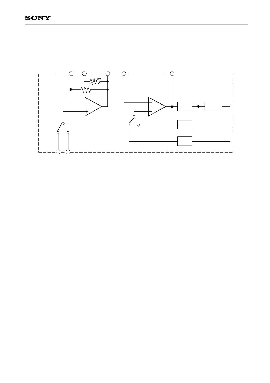
Description of Operation
1. Signal route
Fig. 1
Op1 and Op2 are operational amplifiers.
Op1 composes the playback equalizer by attaching a resistor and a capacitor to PBFB pin, and a
capacitor to PBTC pin.
Op2 is an input selector and a LINEOUT amplifier. The gain is 24 dB.
The Dolby reference level is ≠6 dBm (LINEOUT).
The adjustment method of playback equalizer is described in the paragraph (3).
Note)
Usually the TAPEIN pin level is adjusted by attenuator connected to PBOUT pin.
The capacitance value connected to PBFB can be reduced by adjusting the resistance
connected to PBFB to match the PBOUT level.
With this method, the capacitance value can be reduced according to the amount that the
resistance value is increased even for the same cut-off frequency.
(These specifications use the latter method.)
Op2
4dB
20dB
20dB
NR OFF
NR ON
Op1
PBFB PBTC
PBOUT
TAPEIN
Dolby level
(≠6dBm)
LINEOUT
PBIN
F
R
NR
--12--
CXA1911Q
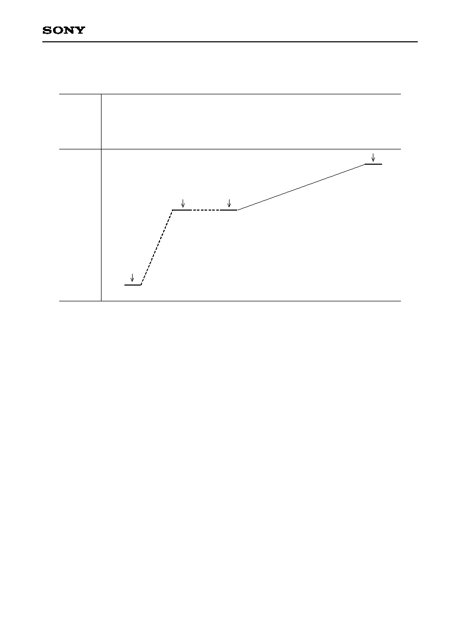
2. Level diagram
Fig.2
Note)
This diagram illustrates the case where the Dolby level is aligned by adjusting the resistance
value connected to PBFB.
≠10
≠15
≠20
≠25
≠30
≠35
≠40
≠45
≠50
≠55
≠60
≠65
≠70
≠75
P
B
I
N
VR adjustment
≠30dBm
≠30dBm
≠6dBm
Dolby level
≠70dBm (315Hz 160nWb/m)
≠5
P
B
O
U
T
T
A
P
E
I
N
L
I
N
E
O
U
T
0dB
--13--
CXA1911Q
3. PBEQ adjustment
1) EQ curve gain difference (=adjustment of internal variable R)
IREF resistor
To adjust the EQ curve gain differences (G1 ≠ G2, G1 ≠ G3), the E IREF resistor should be adjusted to
change the internal variable resistance value.
2) AC gain
External resistor R1
The external resistor R1 should be adjusted to adjust the AC gain.
G1 is obtained by the following equation.
G1=20log
R1 + R3
(R3 = 300k
)
R1
3) Low-band cut-off frequency
External resistor R1 and capacitor C1
The low-band cut-off frequency (fc) can be determined by the external resistor R1 and external capacitor
C1.
Note)
In this diagram, C1 and R1 are not connected in series, but are connected to PBFB from between
R1 and C2.
This is to prevent the sound quality from deteriorating when using an electrolytic capacitor.
R1
C2
C1
PBFB
PBTC
PBOUT
E IREF
R4
1
PBIN
F
R
Ri
3
2
1
fc
2
3
R3
3

--14--
CXA1911Q
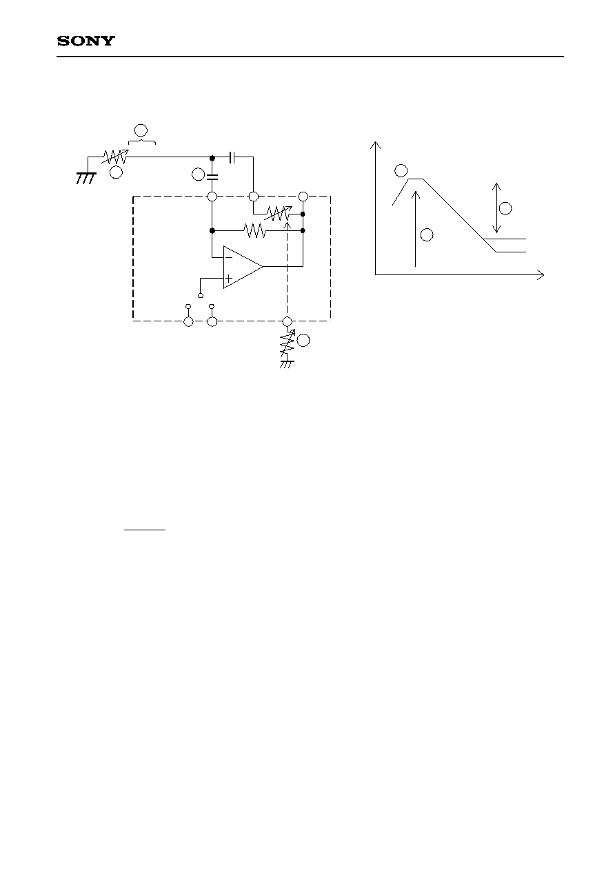
4. MS (internal detection between tracks) adjustment method
1) MS gain (FF/NOR mode gain) adjustment
External resistors R1 and R2
MS gain is expressed by the following equations.
G1 = 10 + 20log
R1 + 100k
[dB]
G2 = 10 + 20log
R2 + 100k
[dB]
R1
R2
2) MS low-band cut-off frequency adjustment
External resistors R1 and R2 and external capacitors C1 and
C2
The external resistors R1 and R2 and external capacitors C1 and C2 should be adjusted to adjust the low-
band cut-off frequency for the MS frequency response.
3) MS high-band cut-off frequency adjustment
External capacitor C3
The external capacitor C3 should be adjusted to adjust the high-band cut-off frequency for the MS
frequency response. (In this case, G1 and G2 have the same cut-off frequency.)
DET
G2
G1
MSOUT
TAPEIN
10dB
25kHz LPF
(in the case of built-in only)
100k
G1
G2
R1
R2
C1
C2
2
1
MSTC
2
1
2
1
2
1
100k
64pF
3
3
MSLPF
C3
--15--
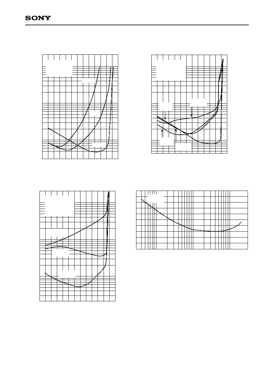
CXA1911Q
20
16
12
8
4
0
C typ e decode characteristics
D
e
c
ode boos
t
[
d
B
]
24
≠40dB
≠30dB
≠20dB
≠10dB
0dB
50
100
1k
10k
Frequency [Hz]
500
5k
≠4
Ta=25∞C
≠60dB
≠50dB
V
CC
=8.0V
0dB=Dolby Level
10
8
6
4
2
0
B typ e decode characteristics
D
e
c
ode boos
t
[
d
B
]
12
≠40dB
≠30dB
≠20dB
≠10dB
0dB
50
100
1k
10k
Frequency [Hz]
500
5k
V
CC
=8.0V
0dB=Dolby Level
OUT
300k
0.01µ
33µ
270
Supply voltage [V]
7.0
8.0
9.0
10.0 11.0 12.0
C
u
r
r
ent
c
ons
um
pt
i
on [
m
A
]
Current consump tion vs. Sup p ly voltage
50
100
1k
Playb ack equalizer frequency resp onse
Ga
i
n
[d
B
]
Frequency [Hz]
60
50
40
30
V
CC
=8.0V
NR OFF, MS OFF
Output level 25dBm constant
120µs
70µs
Ta=25∞C
Ta=25∞C
6.0
5.0
13.0
10k
20.5
21.0
21.5
22.0
For no signal
NR OFF, MS OFF
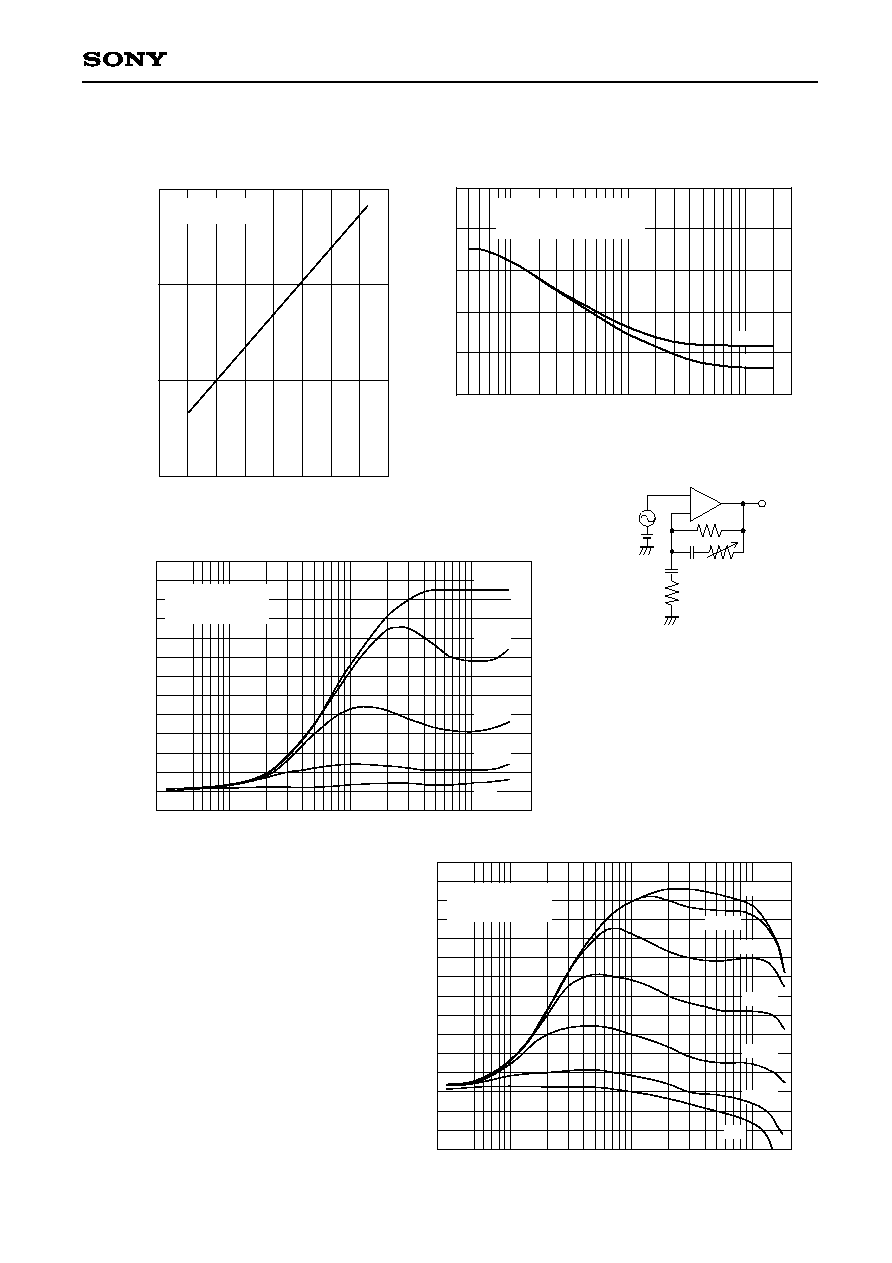
Characteristics Graphs
--16--
CXA1911Q
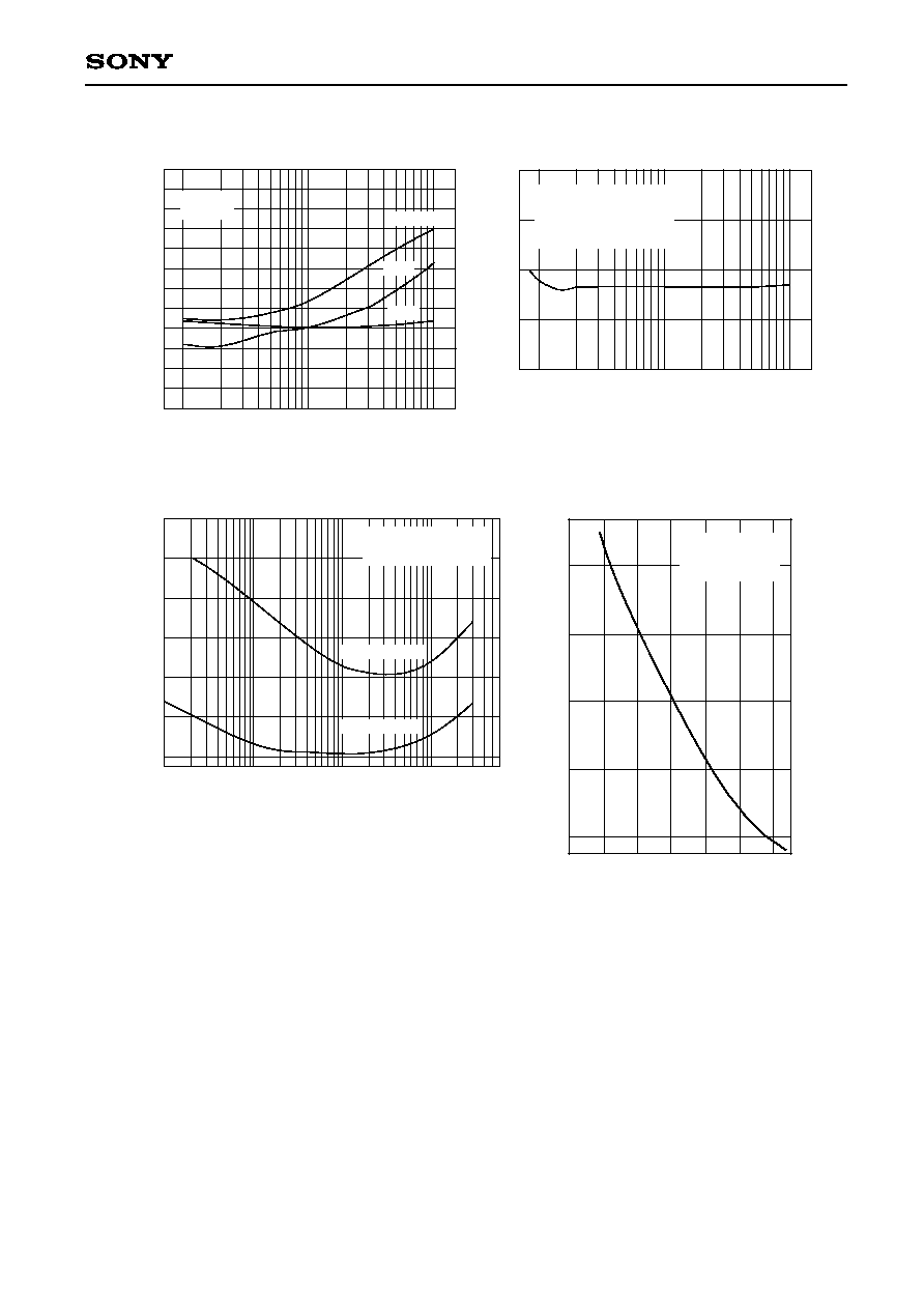
C typ e total harmonic distortion
Ta=25∞C
100
101
T
o
t
a
l
har
m
oni
c
di
s
t
or
t
i
on [
%
]
10-1
10-2
NR C
f=10kHz
NR C
f=100kHz
NR C
f=1kHz
≠8
≠4
0
4
8
12
Total harmonic distortion (p re-amp lifier b lock)
T
o
t
a
l
har
m
oni
c
di
s
t
or
t
i
on [
%
]
Output level [dBm]
≠24
≠20
≠16
≠12
≠8
≠4
0
100
101
10-1
Ta=25∞C
f=10kHz
f=1kHz
f=100Hz
10-2
10-1
B typ e total harmonic distortion
Ta=25∞C
100
≠8
≠4
0
4
8
12
14
NR OFF
f=1kHz
NR B
f=100kHz
NR B
f=1kHz
NR B
f=10kHz
T
o
t
a
l
har
m
oni
c
di
s
t
or
t
i
on [
%
]
Output level [dB]
Ta=25∞C
≠20
≠10
≠30
≠40
≠50
≠60
50
100
1k
10k
500
5k
Rip p le rejection ratio (PB O UT)
Frequency [Hz]
R
i
ppl
e el
i
m
i
nat
i
on r
a
t
i
o [
d
B
]
Output level [dB]
V
CC
=8.0V
Input : PBFIN1
Output : PBOUT1
R
L
=2.7k
Input : TAPEIN1
Output : LINEOUT1
V
CC
=8.0V
0dB=Dolby Level
R
L
=2.7k
Input : TAPEIN1
Output : LINEOUT1
V
CC
=8.0V
0dB=Dolby Level
R
L
=2.7k
Vcc=8.0V
RL=2.7k
--17--
CXA1911Q
≠70
≠60
≠50
≠40
≠30
10
20
30
40
50
60
MS b lock gain vs. B lank detection level
I
nput
l
e
v
e
l
[
d
B
m
]
HPF gain [dB]
V
CC
=8.0V
Input : TAPEIN1
f=1kHz
Ta=25∞C
0
≠10
≠20
≠30
≠40
≠50
≠60
20
100
1k
10k
B lank detection level frequency resp onse
Frequency [HZ]
Ta = 25∞C
HPF Gain 20 dB
HPF Gain 40 dB
I
nput
l
e
v
e
l
[
d
B
m
]
V
CC
= 8.0 V
Input : TAPEIN 1
MSLPF Pin: T120 pF
Cross talk b etween channels (1ch
2ch)
C
r
o
s
s
ta
l
k
[d
B
]
Frequency [Hz]
≠70
1k
100
5k
≠60
≠50
≠40
≠30
Ta=25 ∞C
Vcc=8.0V
Input : PBFIN1
Output : LINEOUT2
(LINEOUT1 level constant)
NR OFF
500
10k
≠70
≠60
≠50
≠40
≠30
≠20
≠10
Ta=25∞C
1k
100
10k
500
5k
NR B
NR C
Rip p ler rejection ratio (LINEO UT)
R
i
ppl
e el
i
m
i
nat
i
on r
a
t
i
o [
d
B
]
Frequency [Hz]
NR OFF
V
CC
=8.0V
R
L
=2.7k
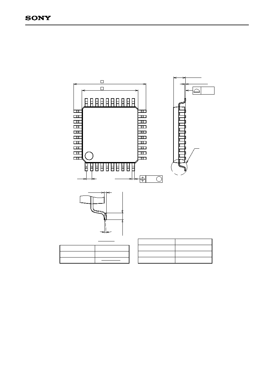
SONY CODE
EIAJ CODE
JEDEC CODE
PACKAGE MATERIAL
LEAD TREATMENT
LEAD MATERIAL
PACKAGE WEIGHT
EPOXY RESIN
SOLDER / PALLADIUM
COPPER / 42 ALLOY
PACKAGE STRUCTURE
PLATING
0.2g
QFP-40P-L01
QFP040-P-0707
40PIN QFP (PLASTIC)
9.0 ± 0.4
+ 0.4
0.3 ≠ 0.1
0.65
1
10
11
20
21
30
31
40
1.5 ≠ 0.15
+ 0.35
0.127 ≠ 0.05
+ 0.1
(8.0)
A
A
DETAIL
0.1 ≠ 0.1
+ 0.15
+ 0.15
7.0 ≠ 0.1
0.5 ±
0.2
0.1
M
± 0.12
Package Outline Unit : mm
CXA1911Q
--18--