 | –≠–ª–µ–∫—Ç—Ä–æ–Ω–Ω—ã–π –∫–æ–º–ø–æ–Ω–µ–Ω—Ç: CXA1998BQ | –°–∫–∞—á–∞—Ç—å:  PDF PDF  ZIP ZIP |
Description
The CXA1998BQ is an IC developed for analog
signal processing in tape recorders. Processing for
both the recording and playback systems is
achieved on one chip.
Features
∑ 11-bit serial data interface
∑ Recording/playback mute function
∑ Recording equalizer Gp and Fp can be adjusted
externally.
∑ AGC (Automatic Gain Control)
∑ Comparator for AMS (Automatic Music Sensor)
∑ Recording/playback equalizer amplifier with 1.7
times speed switching
Absolute Maximum Ratings (Ta = 25∞C)
∑ Supply voltage
V
CC
, V
DD
12
V
∑ Operating temperature
Topr
≠20 to +75
∞C
∑ Storage temperature
Tstg
≠65 to +150
∞C
∑ Allowable power dissipation
P
D
645
mW
Operating Conditions
Supply voltage
V
CC
6.5 to 10.0
V
V
DD
4.5 to 5.5
V
Structure
Bipolar silicon monolithic IC
Applications
All analog signal processing in the cassette decks
of tape recorders and compact music centers
Applicable Head
Applicable to MITSUMI ELECTRIC Co., Ltd.
Playback head: BP-7442-CP-6973
Recording/playback head: BC-9242-CB-9267
≠ 1 ≠
CXA1998BQ
E98Z31-PS
Recording/Playback Equalizer Amplifier
Sony reserves the right to change products and specifications without prior notice. This information does not convey any license by
any implication or otherwise under any patents or other right. Application circuits shown, if any, are typical examples illustrating the
operation of the devices. Sony cannot assume responsibility for any problems arising out of the use of these circuits.
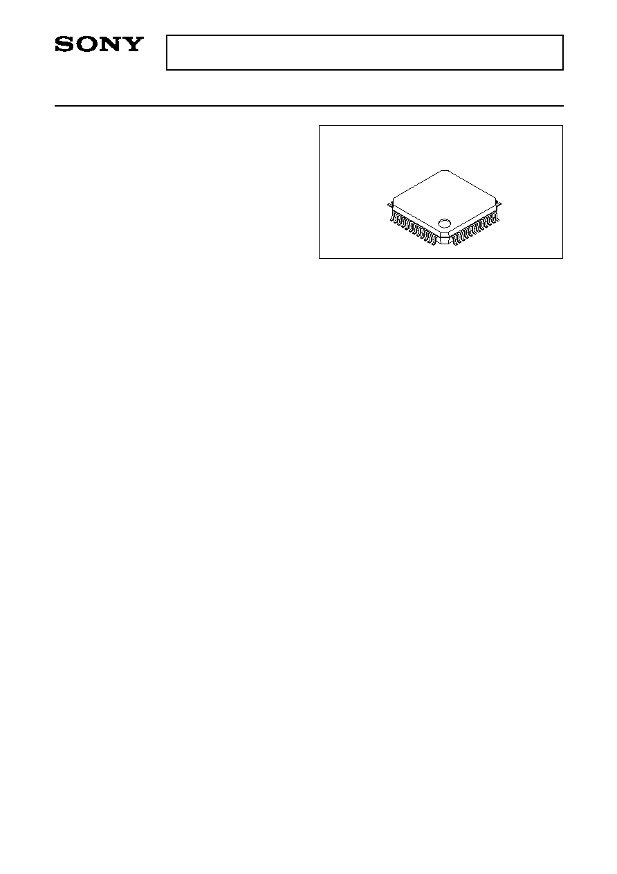
48 pin QFP (Plastic)
≠ 2 ≠
CXA1998BQ
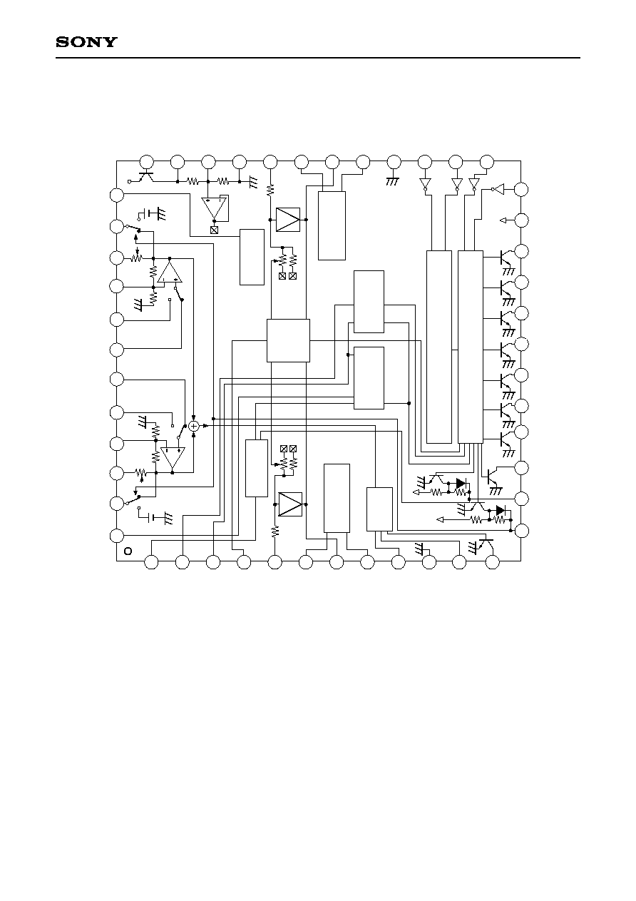
Block Diagram and Pin Configuration (Top View)
D1
D2
D3
D4
D5
D6
2
3
4
5
6
7
8
9
10
11
12
13
14
15
16
17
18
19
20
21
22
23
24
25
26
27
28
29
30
31
32
1
37
38
39
40
41
42
43
44
45
46
47
48
M
U
T
E
A
G
C
G
A
I
N
1
9
.
5
d
B
10k
4
0
k
R
E
C
E
Q
A
M
S
G
N
D
G
N
D
GND
V
DD
V
DD
20k
20k
20k
20k
D11
D9
D10
D8
GND
D7
G
N
D
D11
GND
D9
GND
GND
GND
GND
GND
GND
V
DD
GND
4
0
k
A
G
C
G
A
I
N
1
9
.
5
d
B
1
0
k
R
E
C
E
Q
I
R
E
F
36
35
34
33
G
N
D
RFS
2
.
8
V
2
1
0
k
G
N
D
G
N
D
2
1
0
k
G
N
D
2
1
0
k
2
1
0
k
G
N
D
2
.
8
V
A
G
C
A
G
C
O
F
F
A
E
Q
B
E
Q
P
B
E
Q
C
T
L
R
E
C
E
Q
C
T
L
D
E
C
K
A
/
B
S
P
E
E
D
S
H
I
F
T
R
E
G
I
S
T
E
R
S
L
A
T
C
H
E
S
G
P
C
A
L
A
E
Q
B
E
Q
A
G
C
T
C
A
G
C
I
N
1
R
E
C
I
N
1
A
G
C
O
U
T
1
R
E
C
O
U
T
1
A
M
S
G
A
I
N
A
M
S
G
N
D
A
M
S
T
C
A
M
S
O
U
T
PBMUTE
RMUTEI
RMUTE
SPEED
BPA
BPB
PL1
PL2
M1
M2
V
DD
LATCH
R
F
C
V
c
c
V
G
G
N
D
A
G
C
I
N
2
R
E
C
I
N
2
A
G
C
O
U
T
2
R
E
C
O
U
T
2
D
G
N
D
X
R
E
S
E
T
D
A
T
A
C
L
K
FP CAL
PB OUT1
PB FB21
PB FB11
PB INB1
PB INA1
PB INA2
PB INB2
PB FB12
PB FB22
PB OUT2
IREF
≠ 3 ≠
CXA1998BQ
Pin Description
Pin
No.
1
Symbol
DC
voltage
I/O
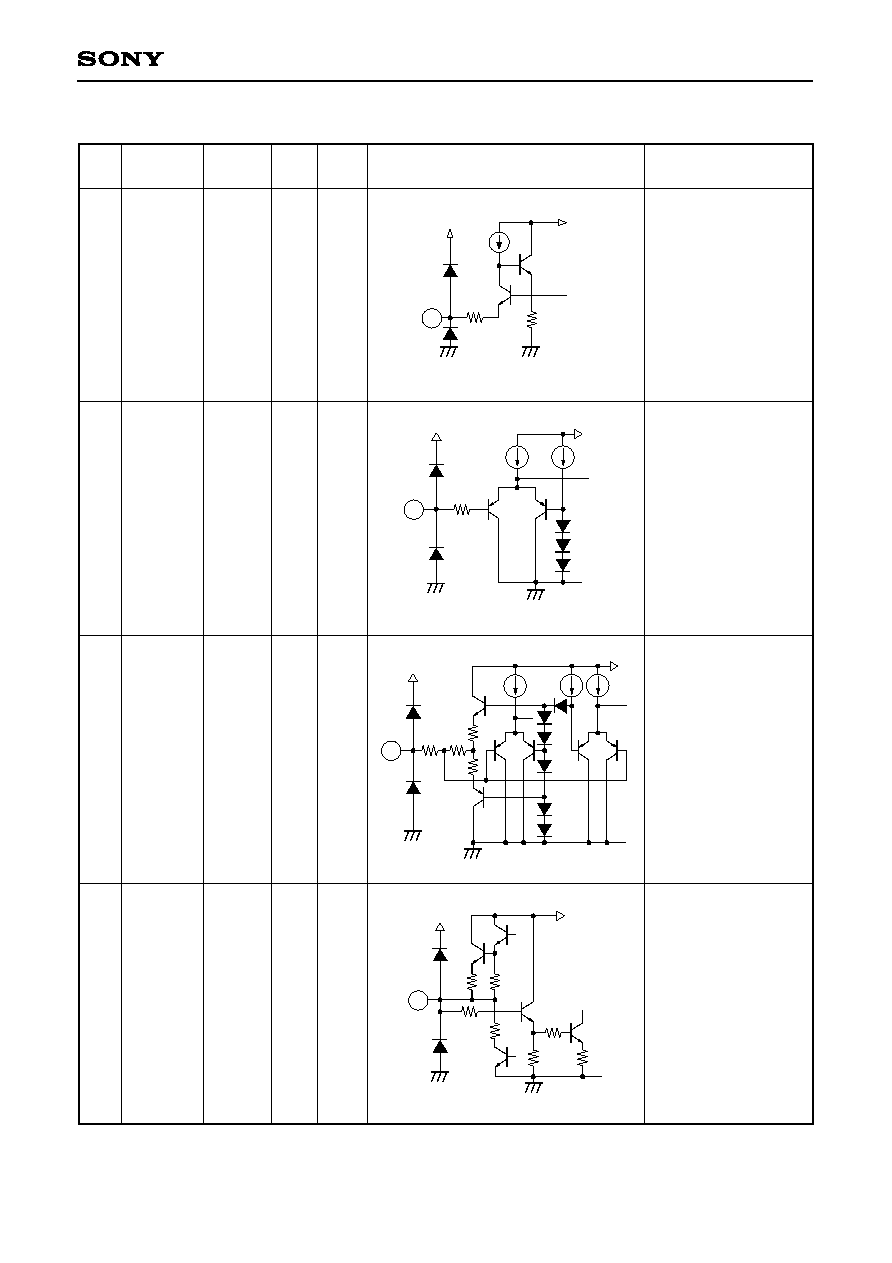
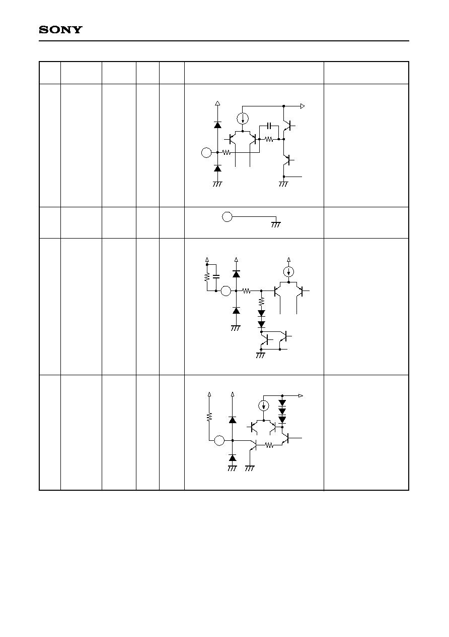
Equivalent circuit
Description
GP CAL
1.2V
--
Connects a resistor
for determining the
high-band peak gain
of recording equalizer.
Reference setting
resistance is 27k
.
I/O
resistance
--
2
A EQ
--
I
Deck A equalizer
switch.
Low: 120µs EQ
High: 70µs EQ
--
3
B EQ
2.5V
(OPEN)
I
Deck B equalizer
switch.
Low: NORMAL TAPE,
120µs EQ
Medium: Cro
2
TAPE,
70µs EQ
High: METAL TAPE,
70µs EQ
53k
4
AGC TC
0.0V
--
Connects a resistor
and capacitor for
determining AGC
attack/recovery time
constants.
--
1
Vcc
Vcc
GND
GND
147
◊
2
30k
V
CC
147
GND
GND
V
CC
2
V
CC
147 50k
V
CC
GND
GND
5k
5k
3
V
CC
GND
GND
V
CC
◊
2
200
100k
500
500
◊
2
147
◊
2
◊
4
200
5k
4
(Ta = 25∞C, V
CC
= 8V, V
DD
= 5V, no signal, RESET ON)

≠ 4 ≠
CXA1998BQ
5
32
AGC IN1
AGC IN2
4.0V
I
AGC signal input.
Input resistance
changes between
50k
and 100k
.
AGC functions when
the signal of ≠30dBm
or more is input to
AGC for AGC ON.
(External 47µF//300k
for Pin 4)
50k
6
31
REC IN1
REC IN2
4.0V
I
Recording equalizer
input.
50k
7
30
AGC OUT1
AGC OUT2
4.0V
O
AGC output.
147
8
29
REC OUT1
REC OUT2
4.0V
O
Recording equalizer
output.
147
V
CC
147
40k
500
◊
10
V
CC
GND
GND
◊
3
500
◊
2
5p
8
29
V
CC
147
18752
500
◊
4
V
CC
GND
VGS
GND
◊
2
500
7
30
107423
9945
VGS
V
CC
147
50k
V
CC
GND
VGS
23186
1759
VGS
GND
6
31
V
CC
147
10k
40k
◊
4
V
CC
GND
VGS
5
32
Pin
No.
Symbol
DC
voltage
I/O
Equivalent circuit
Description
I/O
resistance
≠ 5 ≠
CXA1998BQ
AMS block ground.
9
AMS GAIN
3.5V
--
Connects a resistor
for determining AMS
signal detection level
and a capacitor for
determining HPF cut-
off frequency.
--
10
AMS GND
0.0V
--
--
12
AMS OUT
8.0V
O
AMS output.
No signal detection:
High
Signal detection: Low
--
11
AMS TC
8.0V
--
Connects time
constant for AMS
detection.
--
V
CC
147
GND
V
CC
GND
100k
10µ
9
11
Vcc
GND
1k
GND
147
Vcc
Vcc
GND
Vcc
12
Vcc
Vcc
10k
GND
10
GND
Pin
No.
Symbol
DC
voltage
I/O
Equivalent circuit
Description
I/O
resistance

≠ 6 ≠
CXA1998BQ
13
PBMUTE
14
RMUTE1
5.0V
--
Connects a capacitor
for setting time
constant for playback
mute ON/OFF
switching.
--
15
RMUTE
Output for recording
mute ON/OFF switch
control signal. Outputs
D11 from Pin 26
(DATA).
16
SPEED
5.0V
O
Output for
recording/playback
equalizer speed switch
control signal. Outputs
D9 from Pin 26 (DATA).
Low: Normal Speed
High: High Speed
(1.7 times)
--
17
BPA
5.0V
O
Outputs D6 from
Pin 26 (DATA).
18
BPB
Outputs D5 from
Pin 26 (DATA).
19
PL1
Outputs D4 from
Pin 26 (DATA).
20
PL2
Outputs D3 from
Pin 26 (DATA).
21
M1
Outputs D2 from
Pin 26 (DATA).
22
M2
Outputs D1 from
Pin 26 (DATA).
23
V
DD
Power supply of serial
data interface block.
--
5.0V
--
--
13
14
V
DD
V
DD
20k
20k
GND
◊
4
147
GND
GND
Connects a capacitor
for setting time
constant for recording
mute ON/OFF
switching.
◊
4
V
DD
5k
GND
GND
V
DD
◊
4
5k
20k
15
16
◊
4
V
DD
GND
GND
V
DD
◊
4
10k
20k
17
18
19
20
21
22
V
DD
23
Pin
No.
Symbol
DC
voltage
I/O
Equivalent circuit
Description
I/O
resistance

≠ 7 ≠
CXA1998BQ
24
LATCH
27
XRESET
--
I
Serial data interface
latch input.
--
25
DATA
--
I
Serial data interface
reset input.
Low: Reset.
At this time serial
data outputs
(Pins 15 to 22)
are all open
(high).
--
26
Serial data interface
clock input.
Serial data interface
serial data input.
28
DGND
0.0V
--
Serial data interface
block ground.
--
CLK
2k
GND
V
DD
10.5k
25µA
GND
30k
5p
◊
4
30k
24
27
4k
GND
V
DD
10.5k
25µA
GND
30k
◊
4
30k
25
26
GND
28
33
GND
0.0V
--
Ground.
--
35
V
CC
8.0V
--
Power supply.
--
34
VG
4.0V
--
Signal reference
voltage. Connects a
capacitor for ripple
rejection.
60k
GND
33
34
V
CC
147
45k
30k
◊
4
V
CC
GND
GND
500
500
◊
2
30k
◊
2
T
o
e
a
c
h
V
G
S
35
V
CC
Pin
No.
Symbol
DC
voltage
I/O
Equivalent circuit
Description
I/O
resistance

≠ 8 ≠
CXA1998BQ
Connects a resistor
(12k
) for determining
equalizer gains.
36
RFC
8.0V
--
Connects a resistor
and capacitor for
obtaining stable
voltage with power
supply ripple rejected.
--
37
IREF
38
47
PB OUT2
PB OUT1
2.8V
O
Playback equalizer
output.
147
48
FP CAL
1.2V
--
Connects a resistor for
determining the high-
band peak frequency
of recording equalizer.
Reference setting
resistance is 27k
.
--
36
V
CC
147
V
CC
GND
◊
3
◊
250
◊
3
To each RFS
Vcc
GND
◊
2
GND
37
48
147
5
p
Vcc
Vcc
GND
Vcc
◊
3
500
147
◊
6
GND
15p
47
38
500
39
46
PB FB22
PB FB21
2.8V
--
Connects a capacitor
for determining
playback equalizer
time constants, such
as 120µs and 70µs.
--
39
46
V
CC
147
◊
3
GND
2k
2k
GND
GND
◊
4
7k
◊
3
◊
4
RFS
Pin
No.
Symbol
DC
voltage
I/O
Equivalent circuit
Description
I/O
resistance
≠ 9 ≠
CXA1998BQ
40
45
PB FB12
PB FB11
1.4V
--
Playback equalizer
negative feedback.
105k
41
42
43
44
PB INB2
PB INA2
PB INA1
PB INB1
0.0V
I
Playback equalizer
input.
70k
41
42
43
44
45
70k
10p
V
CC
GND
V
CC
GND
◊
6
V
CC
40
GND
1k
1k
210k
210k
V
CC
RFS
◊
2
10k
5k
◊
6
147
30p
147
Note)
∑ AMS GND (Pin 10), DGND (Pin 28) and GND (Pin 33) are each independent in the IC and are not connected.
Be sure tp ground each of the ground pins listed above.
∑ The resistance of open collector outputs (Pins 15 to 22) can be connected Vcc.
Pin
No.
Symbol
DC
voltage
I/O
Equivalent circuit
Description
I/O
resistance

≠ 10 ≠
CXA1998BQ
Electrical Characteristics
(Ta = 25∞C, V
CC
= 8.0V, V
DD
= 5.0V, refer to Electrical Characteristics Measurement Circuit)
Item
Operating voltage
Current consumption
Measurement conditions
Min.
Typ.
Max.
Unit
V
CC
V
DD
Sum of V
CC
and V
DD
pin currents
NORM ≠ NS, no signal
Pin 4 external R300k
//C47µF
f = 1kHz, Vin = ≠25dBm
Pin 4 external R300k
//C47µF
f = 1kHz, Vin = ≠25dBm
Pin 4 external R300k
//C47µF
f = 1kHz, Vin = 0dBm
Pin 4 external R300k
//C 47µF
f = 1kHz, Vin = ≠25dBm
Pin 9 external R9.1k
, C0.015µF
Pin 11 external R100k
//C0.1µF
f = 5kHz, 0dB = ≠21dBm
(at PBEQ reference output level)
f = 315Hz, Vin = ≠70dBm
Reference for frequency response
f = 2.7kHz, Vin = ≠58.5dBm
at 120µs ≠ NS, 315Hz
f = 4.5kHz, Vin = ≠53.8dBm
at 120µs ≠ NS, 315Hz
f = 5.3kHz, Vin = ≠52.5dBm
at 120µs ≠ NS, 315Hz
f = 9.1kHz, Vin = ≠47.8dBm
at 120µs ≠ NS, 315Hz
120µs ≠ NS, R
L
= 2.7k
f = 1kHz, THD + N = 1%
120µs ≠ NS, R
L
= 2.7k
f = 1kHz, Vin = ≠56.0dBm
120µs ≠ NS, Rg = 470
"A" weighting filter
120µs ≠ NS, Rg = 470
, playback mute OFF
120µs ≠ NS, f = 1kHz, Vin = ≠51.0dBm
AGC ON
output level
AGC ON
channel balance
AGC ON distortion
AGC OFF
output level
No signal detection
threshold level
120µs ≠ NS
frequency response
120µs ≠ NS
frequency response
70µs ≠ NS
frequency response
120µs ≠ HS
frequency response
70µs ≠ HS
frequency response
Signal handling
Total harmonic
distortion
S/N ratio
Output offset voltage
Playback mute
characteristics
6.5
4.5
13.5
≠13.0
≠2.0
--
≠7.5
≠11.5
≠23.0
≠0.6
≠1.2
1.8
2.1
≠10.0
--
55.0
2.4
--
8.0
5.0
19.7
≠11.0
0.0
0.3
≠5.5
≠8.2
≠21.0
0.8
0.6
3.0
3.6
≠6.0
0.3
62.0
2.7
≠100
10.0
5.5
25.0
≠9.0
2.0
1.5
≠3.5
--
≠19.0
2.4
1.8
4.8
5.1
--
0.7
--
3.2
≠80
V
V
mA
dBm
dB
%
dBm
dB
dBm
dB
dBm
%
dB
V
dB
AGC
AMS
Playback equalizer amplifier block

≠ 11 ≠
CXA1998BQ
Reference input level
Reference output level
Channel balance
NORM ≠ NS
frequency response
NORM ≠ NS
frequency response
NORM ≠ NS
frequency response
CrO
2
≠ NS
frequency response
CrO
2
≠ NS
frequency response
CrO
2
≠ NS
frequency response
METAL ≠ NS
frequency response
METAL ≠ NS
frequency response
METAL ≠ NS
frequency response
NORM ≠ HS
frequency response
NORM ≠ HS
frequency response
NORM ≠ HS
frequency response
CrO
2
≠ HS
frequency response
CrO
2
≠ HS
frequency response
CrO
2
≠ HS
frequency response
METAL ≠ HS
frequency response
METAL ≠ HS
frequency response
METAL ≠ HS
frequency response
dB
NORM ≠ NS, 315Hz, input level at which
reference output can be obtained
NORM ≠ NS, 315Hz
NORM ≠ NS, 315Hz, output level
difference 1ch-2ch for ≠27.7dBm input
f = 3kHz at NORM ≠ NS,
315Hz, reference output ≠20dB
f = 8kHz at NORM ≠ NS,
315Hz, reference output ≠20dB
f = 12kHz at NORM ≠ NS,
315Hz, reference output ≠20dB
f = 3kHz at NORM ≠ NS,
315Hz, reference output ≠20dB
f = 8kHz at NORM ≠ NS,
315Hz, reference output ≠20dB
f = 12kHz at NORM ≠ NS,
315Hz, reference output ≠20dB
f = 3kHz at NORM ≠ NS,
315Hz, reference output ≠20dB
f = 8kHz at NORM ≠ NS,
315Hz, reference output ≠20dB
f = 12kHz at NORM ≠ NS,
315Hz, reference output ≠20dB
f = 5kHz at NORM ≠ NS,
315Hz, reference output ≠20dB
f = 15kHz at NORM ≠ NS,
315Hz, reference output ≠20dB
f = 20kHz at NORM ≠ NS,
315Hz, reference output ≠20dB
f = 5kHz at NORM ≠ NS,
315Hz, reference output ≠20dB
f = 15kHz at NORM ≠ NS,
315Hz, reference output ≠20dB
f = 20kHz at NORM ≠ NS,
315Hz, reference output ≠20dB
f = 5kHz at NORM ≠ NS,
315Hz, reference output ≠20dB
f = 15kHz at NORM ≠ NS,
315Hz, reference output ≠20dB
f = 20kHz at NORM ≠ NS,
315Hz, reference output ≠20dB
≠27.7
≠10.0
0.0
≠1.7
3.5
10.2
3.2
9.0
15.8
4.0
8.1
12.8
≠0.8
8.7
13.9
5.4
15.2
18.7
7.0
14.5
18.4
≠29.2
--
≠1.5
≠2.9
2.1
7.6
1.9
7.1
12.5
2.8
6.7
10.9
≠2.6
6.6
10.9
4.2
13.1
15.7
5.8
12.7
15.9
≠26.2
--
1.5
≠0.5
5.7
14.6
4.3
11.1
21.0
5.2
9.7
15.9
1.2
10.8
16.4
6.6
17.3
21.7
8.2
16.3
20.9
dBm
Recording equalizer amplifier block
Item
Measurement conditions
Min.
Typ.
Max.
Unit

≠ 12 ≠
CXA1998BQ
NORM ≠ NS, R
L
= 2.7k
f = 1kHz, THD + N = 1%
NORM ≠ NS, R
L
= 2.7k
f = 1kHz, 0dB
NORM ≠ NS, Rg = 5.1k
"A" weighting filter
NORM ≠ NS
NORM ≠ NS, f = 1kHz
8dB
A-EQ (Pin 2)
A-EQ (Pin 2)
B-EQ (Pin 3)
B-EQ (Pin 3)
B-EQ (Pin 3)
Signal handling
Total harmonic
distortion
S/N ratio
Output offset voltage
Recording mute
characteristics
8.0
--
57.0
3.6
--
0.0
2.5
0.0
2.2
4.2
8.8
0.2
60.6
4.0
≠100
--
--
--
--
--
--
0.5
--
4.4
≠80
0.5
V
CC
0.5
2.8
V
CC
dB
%
dB
V
Control voltage
low level 1
Control voltage
high level 1
Control voltage
low level 2
Control voltage
medium level 1
Control voltage
high level 2
Note) NORM ≠ NS: NORMAL TAPE ≠ NORMAL SPEED
NORM ≠ HS: NORMAL TAPE ≠ HIGH SPEED
CrO
2
≠ NS: CrO
2
TAPE ≠ NORMAL SPEED
CrO
2
≠ HS: CrO
2
TAPE ≠ HIGH SPEED
METAL ≠ NS: METAL TAPE ≠ NORMAL SPEED
METAL ≠ HS: METAL TAPE ≠ HIGH SPEED
120µs ≠ NS: EQ = 120µs ≠ NORMAL SPEED
120µs ≠ HS: EQ = 120µs ≠ HIGH SPEED
70µs ≠ NS: EQ = 70µs ≠ NORMAL SPEED
70µs ≠ HS: EQ = 70µs ≠ HIGH SPEED
dB
V
Recording equalizer amplifier block
Item
Measurement conditions
Min.
Typ.
Max.
Unit
≠ 13 ≠
CXA1998BQ
V
IL
(LATCH/CLK/DATA/XRESET)
(Pins 24, 25, 26, 27)
V
IH
(LATCH/CLK/DATA/XRESET)
(Pins 24, 25, 26, 27)
V
OL
, I
OL
= 2mA (max)
(Pins 15, 16, 17, 18, 19, 20, 21, 22)
I
OZ
Leak current which flows to the output
pin when I
OZ
output is open; applied
voltage is 10V. (Pins 15 to 22)
(1) f
CK
(2)
t
WC
(3)
t
WR
(4)
t
SDK
(DATA
CLK)
(5)
t
HCD
(CLK
DATA)
(6)
t
WD
(7)
t
SLD
(LATCH
DATA)
(8)
t
HCL
(CLK
LATCH)
(9)
t
HLC
(LATCH
CLK)
Low level
input voltage
High level
input voltage
Low level
output voltage
High level output
off leak current
Maximum clock
frequency
Minimum clock
pulse width
Minimum reset
pulse width
Minimum data
setup time
Minimum data
hold time
Minimum data
pulse width
Minimum latch
setup time
Minimum latch
hold time
Minimum clock
hold time
0.0
3.5
0.0
--
500
--
--
--
--
--
--
--
--
--
--
--
--
--
--
--
--
--
--
--
--
--
1.5
V
DD
0.5
1.0
--
1.0
1.0
1.0
1.0
2.0
1.0
1.0
1.0
Note)
∑ V
DD
is CPU supply voltage of 5.0V.
∑ V
CC
is 10.0V for high level output off-leak current.
∑ The threshold levels of low level input voltage and high level input voltage depend on V
DD
. Input level
detection is done by comparison with V
DD
/2. (Refer to "Equivalent circuit" of Pin Description.)
µs
V
µA
kHz
Item
Measurement conditions
Min.
Typ.
Max.
Unit
11-bit serial data interface block
≠ 14 ≠
CXA1998BQ
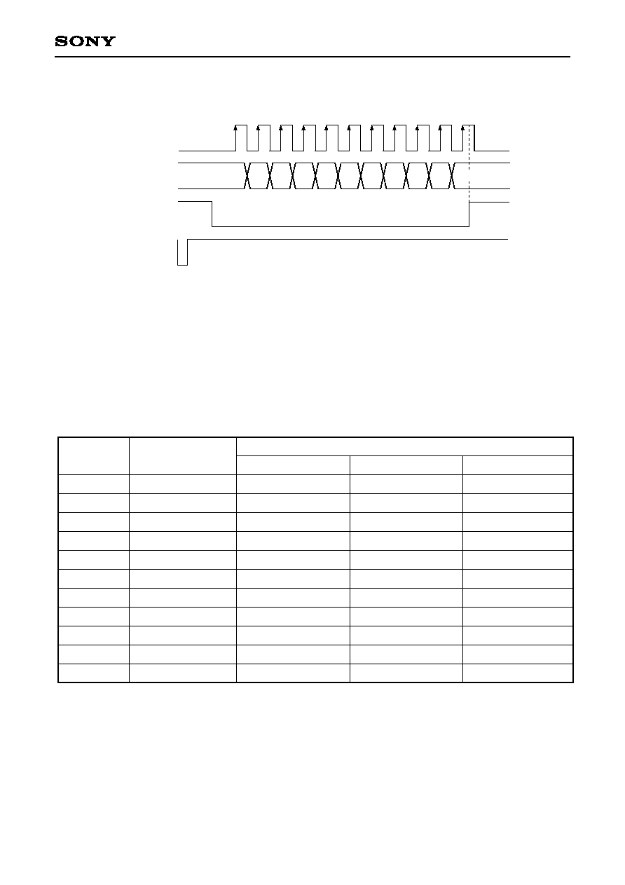
Timing Chart for 11-bit Serial Data Interface (V
DD
= 5.0V)
t
WC
t
WC
t
WD
t
HCD
t
SDK
1.5V
3.5V
D1
D2
1.5V
3.5V
1.5V
t
SLD
3.5V
1.5V
3.5V
1.5V
t
HCL
D10
D11
t
HLC
t
WR
CLK
DATA
LATCH
CLK
DATA
LATCH
XRESET
≠ 15 ≠
CXA1998BQ
Electrical Characteristics
Measurement Circuit
6
7
8
1
1
1
2
1
3
1
4
1
5
1
6
1
7
1
8
1
9
2
0
2
1
2
2
2
4
2
5
2
6
2
7
2
8
2
9
3
0
3
1
3
7
3
9
4
6
4
7
4
8
3
6
3
5
3
4
GP
C
AL
A E
Q
B E
Q
AG
C T
C
AG
C I
N1
RE
C I
N1
AG
C O
UT
1
RE
C O
UT
1
AM
S G
AIN
AM
S G
ND
AM
S T
C
AM
S O
UT
P
B
M
U
T
E
R
M
U
T
E
I
R
M
U
T
E
S
P
E
E
D
B
P
A
B
P
B
P
L
1
P
L
2
M
1
M
2
V
D
D
L
A
T
C
H
RF
C
Vc
c
VG
GN
D
AG
C I
N2
RE
C I
N2
AG
C O
UT
2
RE
C O
UT
2
DG
ND
XR
ES
ET
DA
TA
CL
K
F
P
C
A
L
P
B
O
U
T
1
P
B
F
B
2
1
P
B
F
B
1
1
P
B
I
N
B
1
P
B
I
N
A
1
P
B
I
N
A
2
P
B
I
N
B
2
P
B
F
B
1
2
P
B
F
B
2
2
P
B
O
U
T
2
I
R
E
F
R
1
1
4
1
0
k
R
1
0
3
2
.
2
k
S
3
6
A
S
3
6
B
R
1
1
3
1
0
k
R
1
0
2
2
.
2
k
S
3
5
A
S
3
5
B
R
1
1
2
1
0
k
R
1
0
1
2
.
2
k
S
3
4
A
S
3
4
B
R
1
1
1
R
1
0
0
2
.
2
k
S
3
3
B
R
1
1
0
R
9
9
2
.
2
k
S
3
2
B
R
1
0
9
R
9
8
2
.
2
k
S
3
1
B
1
0
k
S
3
3
A
1
0
k
S
3
2
A
1
0
k
S
3
1
A
R
1
0
8
R
9
7
2
.
2
k
S
3
0
B
1
0
k
S
3
0
A
R
1
0
7
R
9
6
2
.
2
k
S
2
9
B
1
0
k
S
2
9
A
R
1
0
6
C
3
4
0
.
1
µ
S
5
7
A
1
0
k
S
5
3
R
1
0
5
S
5
7
B
1
0
k
S
5
4
C
3
3
0
.
1
µ
S
5
6
B
S
5
6
A
S
5
8
H
S
5
8
G
S
5
8
F
S
5
8
E
S
5
8
D
S
5
8
C
S
5
8
B
S
5
8
A
2
3
5
V
5
V
L
A
T
C
H
2.2
µ
/2
5V
C3
0
2.7
k
R8
6
S1
2D
4.7
µ
/2
5V
C2
8
10
k
R7
9
0.4
7
µ
/5
0V
C2
6
0.4
7
µ
/5
0V
C2
2
10
k
R8
9
S2
7B
10
0
R8
4
S2
7A
10
0
R8
1
S2
1B
R7
6
39
0k
R7
2
47
k
S2
1A
5.1
k
3
2
3
3
10
k
R6
1
47
µ
/2
5V
C1
8
8
V
47
µ
/2
5V
C1
7
47
µ
/2
5V
C1
5
1
k
R
5
B
S1
5
CL
K
DA
TA
XR
ES
ET
3
8
4
0
1
0
0
R
4
4
4
7
µ
/
2
5
V
C
1
0
4
.
7
k
R
3
7
4
7
0
R
5
0
4
1
0.0
18
µ
C1
4
1
µ
C
9
4
.
7
µ
/
2
5
V
C
4
8
2
k
R
3
5
4
7
0
R
4
9
1
µ
C
8
4
.
7
µ
/
2
5
V
C
3
8
2
k
R
3
4
4
7
0
R
4
8
1
µ
C
7
4
.
7
µ
/
2
5
V
C
2
8
2
k
R
3
3
4
7
0
R
4
7
1
µ
C
6
4
.
7
µ
/
2
5
V
C
1
8
2
k
R
3
2
4
2
4
3
4
4
1
0
0
R
4
3
4
7
µ
/
2
5
V
C
5
4
.
7
k
R
3
6
0.0
18
µ
C1
3
4
5
2
.
2
µ
/
2
5
V
C
1
1
2
.
7
k
R
3
8
S
1
2
B
2
7
k
R
4
2
2
.
2
µ
/
2
5
V
2
.
7
k
S
1
2
A
1
2
k
R
4
5
10
0
R4
1
S1
1A
10
k
R5
2
S1
1B
2.2
µ
/2
5V
C2
9
2.7
k
R8
5
S1
2C
10
k
R8
8
S2
6B
10
0
R8
3
S2
6A
4.7
µ
/2
5V
C2
7
10
k
R7
8
S2
2B
0.4
7
µ
/2
5V
C2
5
R7
4
S2
5B
R7
3
39
0k
R7
1
47
k
R8
0
10
0
0.4
7
µ
/5
0V
C2
1
5.1
k
S2
2A
5.1
k
R6
8
30
0k
R6
6
4
5
47
µ
/2
5V
C2
0
3
S2
0
S1
9
S1
8
ME
TA
L
CrO
2
NO
RM
10
k
R6
3
10
k
R5
9
2
4
.
2
V
2
.
5
V
0
.
5
V
27
k
R5
6
1
9.1
k
R9
0
0.0
15
µ
C3
1
9
1
0
0.1
µ
C3
2
10
0k
R9
2
10
0k
R9
3
10
k
R9
4
S2
8
G
N
D
D
C
O
U
T
P
U
T
T
L
0
7
2
+
≠
60
0
R3
0
A
T
T
S
5
B
S
5
A
≠
6
d
B
A
T
T
S
4
B
S
4
A
≠
9
d
B
A
T
T
S
3
B
S
3
A
≠
1
7
d
B
A
T
T
S
2
B
S
2
A
≠
2
9
d
B
A
T
T
S
1
B
S
1
A
≠
4
0
d
B
A
C
I
N
P
U
T
C
H
A
R
G
E
1
C
H
A
R
G
E
2
10
k
R5
1
10
0
R4
0
S1
0B
S1
0A
1
k
H
z
B
a
n
d
P
a
s
s
F
i
l
t
e
r
(
2
0
d
B
)
A
u
d
i
o
(
2
2
.
2
H
z
≠
2
2
.
2
k
H
z
)
F
i
l
t
e
r
"
A
"
W
e
i
g
h
t
i
n
g
F
i
l
t
e
r
3
0
d
B
A
M
P
B
U
F
S
5
0
5
S
5
0
4
S
5
0
3
S
5
0
2
S
5
0
1
A
C
O
U
T
P
U
T
10
0k
R5
36
G
N
D
4
.
7
k
R
5
4
10
k
R6
4
S1
6
5.1
k
R6
9
C2
4
0.1
µ
S2
5A
R7
5
C2
3
0
.1
µ
S
1
4
R
3
9
C
1
2
0.1
µ
C1
6
12
0
µ
s
70
µ
s
S
9
S
8
S
7
S
6
S
1
3
S5
5
S2
3
0.1
µ
C1
9
B E
Q
A E
Q
S1
7
S3
7
S2
4

≠ 16 ≠
CXA1998BQ
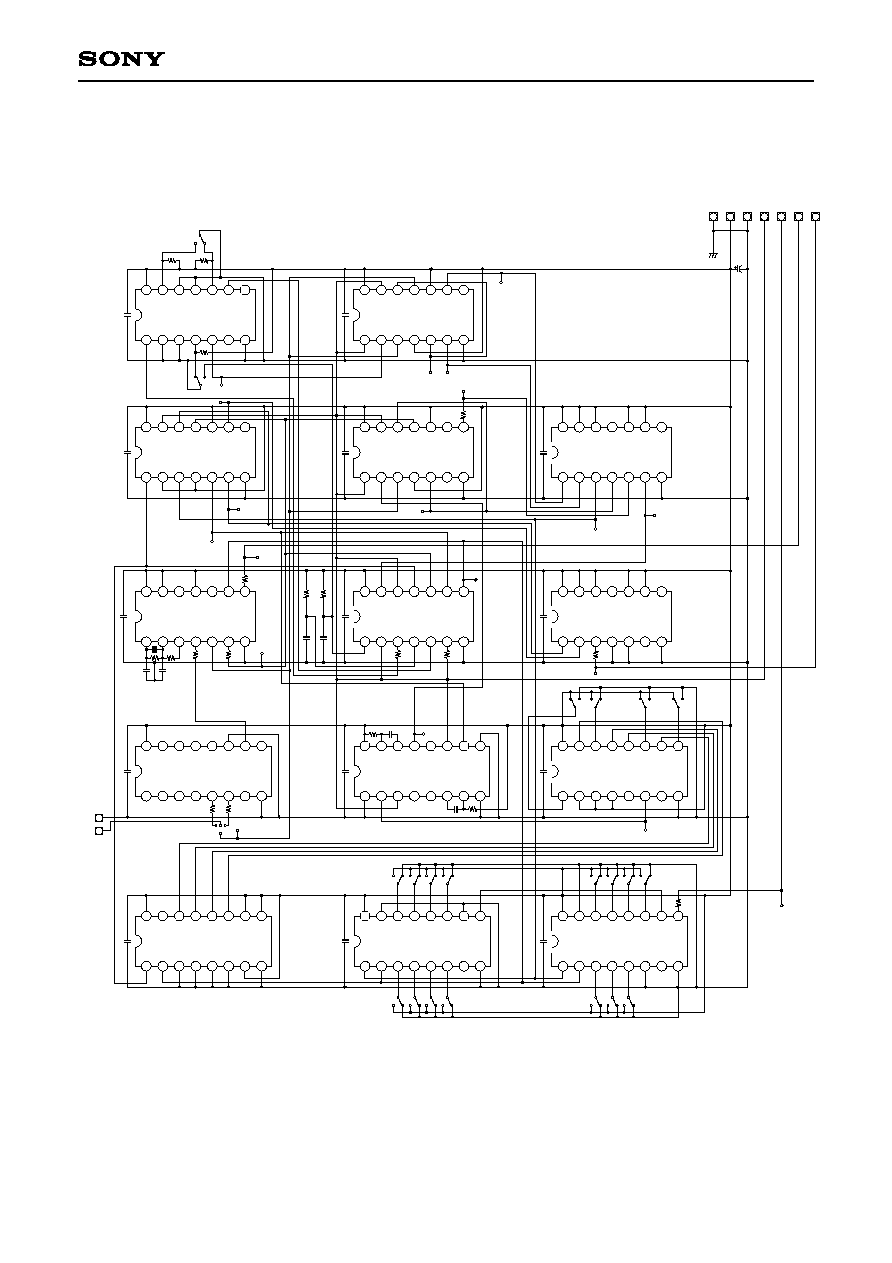
Application Circuit
G
P
C
A
L
A
E
Q
B
E
Q
A
G
C
T
C
A
G
C
I
N
1
R
E
C
I
N
1
A
G
C
O
U
T
1
R
E
C
O
U
T
1
A
M
S
G
A
I
N
A
M
S
G
N
D
A
M
S
T
C
A
M
S
O
U
T
PBMUTE
RMUTEI
RMUTE
SPEED
BPA
BPB
PL1
PL2
M1
M2
V
DD
LATCH
R
F
C
V
c
c
V
G
G
N
D
A
G
C
I
N
2
R
E
C
I
N
2
A
G
C
O
U
T
2
R
E
C
O
U
T
2
D
G
N
D
X
R
E
S
E
T
D
A
T
A
C
L
K
FP CAL
PB OUT1
PB FB21
PB FB11
PB INB1
PB INA1
PB INA2
PB INB2
PB FB12
PB FB22
PB OUT2
IREF
V
DD
100k
V
DD
V
DD
47k
V
DD
47k
V
DD
47k
V
DD
47k
V
DD
47k
V
DD
47k
V
DD
47k
V
DD
47k
GND
0.1µ
GND
22µ
1
0
0
k
1
0
0
k
0
.
1
µ
2
.
2
k
0
.
1
µ
GND
2
7
k
V
CC
3
.
3
m
e
g
4
7
µ
0
.
4
7
µ
0
.
1
µ
2
.
7
k
4.7µ
1
0
k
2
.
2
µ
2.2µ
10k
GND
GND
GND
GND
V
CC
V
CC
GND
27k
47µ
100
GND
0
.
0
1
8
µ
47µ
100
GND
0
.
0
1
8
µ
2.2µ
10k
GND
GND
12k
1
0
0
k
GND
1
0
0
k
GND
1
0
0
k
GND
V
DD
2
.
2
µ
GND
2
.
2
µ
GND
0.1µ
2.7k
4.7µ
10k
0
.
4
7
µ
GND
GND
4
7
µ
GND
4
7
µ
GND
1
0
0
µ
1k
V
CC
B
i
a
s
O
S
C
GND
D
E
C
K
-
A
P
B
-
H
E
A
D
GND
GND
R
/
P
-
H
E
A
D
D
E
C
K
-
B
GND
150p
8
2
0
p
1
0
k
1
8
0
p
1
2
m
H
GND
150p
1
8
0
p
1
2
m
H
8
2
0
p
1
0
k
D1
D2
D3
D4
D5
D6
2
3
4
5
6
7
8
9
10
11
12
13
14
15
16
17
18
19
20
21
22
23
24
25
26
27
28
29
30
31
32
1
37
38
39
40
41
42
43
44
45
46
47
48
M
U
T
E
A
G
C
G
A
I
N
1
9
.
5
d
B
10k
4
0
k
R
E
C
E
Q
A
M
S
G
N
D
G
N
D
GND
V
DD
V
DD
20k
20k
20k
20k
D11
D9
D10
D8
GND
D7
G
N
D
D11
GND
D9
GND
GND
GND
GND
GND
GND
V
DD
GND
4
0
k
A
G
C
G
A
I
N
1
9
.
5
d
B
1
0
k
R
E
C
E
Q
I
R
E
F
36
35
34
33
G
N
D
RFS
2
.
8
V
2
1
0
k
G
N
D
G
N
D
2
1
0
k
G
N
D
2
1
0
k
2
1
0
k
G
N
D
2
.
8
V
A
G
C
A
G
C
O
F
F
A
E
Q
B
E
Q
P
B
E
Q
C
T
L
R
E
C
E
Q
C
T
L
D
E
C
K
A
/
B
S
P
E
E
D
S
H
I
F
T
R
E
G
I
S
T
E
R
S
L
A
T
C
H
E
S
REC
PB
REC
PB
Application circuits shown are typical examples illustrating the operation of the devices. Sony cannot assume responsibility for
any problems arising out of the use of these circuits or for any infringement of third party patent and other right due to same.
≠ 17 ≠
CXA1998BQ
1. System control mode
Playback and recording equalizer
(1) Playback equalizer (120µs/70µs)
DECK-AB
(serial data
D10 (Pin 25))
A-EQ (Pin 2)
B-EQ (Pin 3)
L
H
L
M/H
L
H
120µs
(DECK A)
70µs
(DECK A)
According to A-EQ control
120µs
(DECK B)
70µs
(DECK B)
According to B-EQ control
(3) Recording equalizer (Normal, CrO
2
, Metal)
B-EQ (Pin 3)
REC MODE
L
NORMAL (TYPE
I
)
M
CrO
2
(TYPE
II
)
H
METAL (TYPE
IV
)
(4) Recording mute (Pin 14)
ON/OFF control is performed by 11-bit serial data interface D11 (Pin 26). A fader function is achieved using a
time constant circuit formed with the external capacitor and incorporated 20k
resistor.
(5) FP CAL (Pin 48)
The standard resistor setting is 27k
, but when resistance value is larger, fo (Hz) is lower, and when
resistance value is smaller, fo (Hz) is higher. (fo: high-band peak frequency)
(6) GP CAL (Pin 1)
The standard resistor setting is 27k
, but when resistance value is larger, high-band peak gain is larger, and
when resistance value is smaller, high-band peak gain is smaller.
(2) Playback mute (Pin 13)
ON/OFF control is performed by 11-bit serial data interface D7 (Pin 26). A capacitor for setting the switching
time constant is connected.
Time constant = 20k
◊
C
≠ 18 ≠
CXA1998BQ
2. 11-bit serial data interface
D1
D2
D3
D4
D5
D6
D7
D8
D9
D10
D11
M2
M1
PL2
PL1
BPB
BPA
PB MUTE
AGC OFF
SPEED
DECK AB
REC MUTE
Pin 22
Pin 21
Pin 20
Pin 19
Pin 18
Pin 17
--
--
Pin 16
--
Pin 15
Low
Low
Low
Low
Low
Low
Low mute OFF
AGC function stops
Low, normal speed
DECK A selected
Low mute OFF
High (OPEN)
High (OPEN)
High (OPEN)
High (OPEN)
High (OPEN)
High (OPEN)
High mute ON
AGC function operates
High (open) 1.7
DECK B selected
High (open) mute ON
Output pin
Input set at low
Input set at high
Output
DATA
(Pin 26)
Control signal
D1
D2
D3
D4
D5
D6
D7
D8
D9
D10
CLK
(Pin 25)
DATA
(Pin 26)
LATCH
(Pin 24)
XRESET
(Pin 27)
D11
∑ The DATA signal is taken in at the rising edge of the CLK signal.
∑ The DATA signal is taken into the internal shift register when the LATCH signal is low. (Outputs (Pins 15 to 22)
hold the previous value while the LATCH signal is low.)
∑ The internal shift register data is latched and output in parallel at the rising edge of the LATCH signal.
(Internal shift register data is loaded while the LATCH signal is high.)
∑ The CLK signal of the 11th bit should fall after the LATCH signal rises.
∑ Reset is done when the XRESET pin is low. (asynchronous method)
Outputs (Pins 15 to 22) are all high (open) during reset.

≠ 19 ≠
CXA1998BQ
∑ Make sure that V
DD
is 4.0V or more and XRESET is 1.5V or less, and 1µs or more when resetting by
applying CR time constant to XRESET (Pin 27) and turning power ON.
1µs or more
1.5V or less
4.0V or more
V
DD
(Pin 23)
XRESET
(Pin 27)
A
1µs or more
5.0V
4.0V or more
V
DD
(Pin 23)
XRESET
(Pin 27)
0V
∑ XRESET (Pin 27) input level detection is done by comparison with V
DD
/2.
The level should be V
DD
/2 > XRESET during the interval A.
∑ For resetting with CPU when power is turned ON
∑ Examples of AGC control during timer recording
(1) Resets when power is turned ON (AGC function operates).
(2) AGC is turned OFF after AGC inputs (Pins 5 and 32) rise.
(External capacitor charge of AGC TC is discharged.)
(3) AGC is turned ON and timer recording begins.
≠ 20 ≠
CXA1998BQ
D
1
1
H
L
D
1
0
H
L
D
9
H
L
D
8
H
L
D
1
2
H
L
D
1
3
H
L
D
1
4
H
L
D
1
5
H
L
6
X
Q
2
Q
2
X
P
R
2
C
L
K
2
D
2
X
R
2
V
D
D
V
S
S
X
Q
1
Q
1
X
P
R
1
C
L
K
1
D
1
X
R
1
74HC74 (1)
X
Q
2
Q
2
X
P
R
2
C
L
K
2
D
2
X
R
2
V
D
D
V
S
S
X
Q
1
Q
1
X
P
R
1
C
L
K
1
D
1
X
R
1
74HC74 (2)
X
Q
2
Q
2
X
P
R
2
C
L
K
2
D
2
X
R
2
V
D
D
V
S
S
X
Q
1
Q
1
X
P
R
1
C
L
K
1
D
1
X
R
1
74HC74 (3)
X
Q
2
Q
2
X
P
R
2
C
L
K
2
D
2
X
R
2
V
D
D
V
S
S
X
Q
1
Q
1
X
P
R
1
C
L
K
1
D
1
X
R
1
74HC74 (4)
Y
3
A
3
B
3
Y
4
A
4
B
4
V
D
D
V
S
S
Y
2
B
2
A
2
Y
1
B
1
A
1
74HC00
Y
3
A
3
B
3
Y
4
A
4
B
4
V
D
D
V
S
S
Y
2
B
2
A
2
Y
1
B
1
A
1
74HC08 (2)
Y
3
A
3
B
3
Y
4
A
4
B
4
V
D
D
V
S
S
Y
2
B
2
A
2
Y
1
B
1
A
1
74HC08 (1)
Y
4
A
4
Y
5
A
5
Y
6
A
6
V
D
D
V
S
S
Y
3
A
3
Y
2
A
2
Y
1
A
1
74HC04
R5
10k
O
N
O
F
F
S
T
A
R
T
3
O
N
O
F
F
R
E
S
E
T
C
5
0
.
1
µ
4
C
1
2
0
.
1
µ
C
9
0
.
1
µ
C
8
0
.
1
µ
R3
10k
R6
10k
C
4
0
.
1
µ
18
C
1
4
0
.
1
µ
C
1
3
0
.
1
µ
C
2
0
0
.
1
µ
5
13
1
0
0
R
1
6
12
7
14
Q
1
C
L
O
C
K
R
E
S
E
T
Q
9
Q
8
Q
1
0
Q
1
1
V
D
D
V
S
S
Q
2
Q
3
Q
4
Q
7
Q
5
Q
6
Q
1
2
74HC4040
X
A
2
B
2
X
R
E
S
2
X
Q
2
Q
1
C
1
R
/
C
1
V
D
D
V
S
S
R
/
C
2
C
2
Q
2
X
Q
1
X
R
E
S
1
B
1
X
A
1
74HC123
B
0
A
0
B
1
A
1
A
2
B
2
A
3
V
D
D
V
S
S
A
<
B
O
U
T
A
=
B
O
U
T
A
>
B
O
U
T
A
>
B
I
N
A
=
B
I
N
A
<
B
I
N
B
3
74HC85
X
L
O
A
D
E
N
A
1
R
E
S
E
T
Q
9
Q
8
Q
1
0
Q
1
1
V
D
D
V
S
S
E
N
A
P
D
D
D
C
D
B
D
A
C
L
O
C
K
X
R
E
S
E
T
74HC161
Q
H
S
E
R
I
A
L
I
N
A
B
C
D
C
L
K
2
V
D
D
V
S
S
X
Q
H
H
G
F
E
C
L
K
1
S
/
X
L
74HC165 (1)
C
1
9
0
.
1
µ
C
1
8
0
.
1
µ
1
2
4
8
H
L
H
L
H
L
H
L
D
4
H
L
D
5
H
L
D
6
H
L
D
7
H
L
Q
H
S
E
R
I
A
L
I
N
A
B
C
D
C
L
K
2
V
D
D
V
S
S
X
Q
H
H
G
F
E
C
L
K
1
S
/
X
L
74HC165 (2)
C
1
7
0
.
1
µ
C
1
1
0
.
1
µ
C
1
0
0
.
1
µ
D
3
H
L
D
2
H
L
D
1
H
L
8
17
68k
R17
11
C16
4.7µ
C15
1000P
R13
2.2k
1
R
7
2
2
0
R
8
2
2
0
R
1
5
2
2
0
R
1
4
2
2
0
R
1
1
1
0
k
R
1
2
1
0
k
9
16
R1
1M
R2
220
C6
15P
C7
15P
4.4MHz
R
4
2
2
0
R
9
2
2
0
2
L
A
T
C
H
C
L
K
D
A
T
A
X
R
E
S
E
T
D
G
N
D
5
V
S
W
G
N
D
GND
100µ/25V
C21
15
10
19
1
0
0
R
1
8
DGND
EXCLK
C
3
0
.
1
µ
C
2
0
.
1
µ
C
0
.
1
µ
EXCLK
2
5
0
k
H
z
5
0
0
k
H
z
1
0
0
R
1
9
1
0
0
R
1
0
8
9
10
11
12
13
14
2
3
4
5
6
7
1
8
9
10
11
12
13
14
2
3
4
5
6
7
1
8
9
10
11
12
13
14
2
3
4
5
6
7
1
8
9
10
11
12
13
14
2
3
4
5
6
7
1
8
9
10
11
12
13
14
2
3
4
5
6
7
1
8
9
10
11
12
13
14
2
3
4
5
6
7
1
8
9
10
11
12
13
14
2
3
4
5
6
7
1
8
9
10
11
12
13
14
2
3
4
5
6
7
1
8
9
10
11
12
13
14
2
3
4
5
6
7
1
15
16
8
9
10
11
12
13
14
2
3
4
5
6
7
1
15
16
8
9
10
11
12
13
14
2
3
4
5
6
7
1
15
16
8
9
10
11
12
13
14
2
3
4
5
6
7
1
15
16
8
9
10
11
12
13
14
2
3
4
5
6
7
1
15
16
8
9
10
11
12
13
14
2
3
4
5
6
7
1
15
16
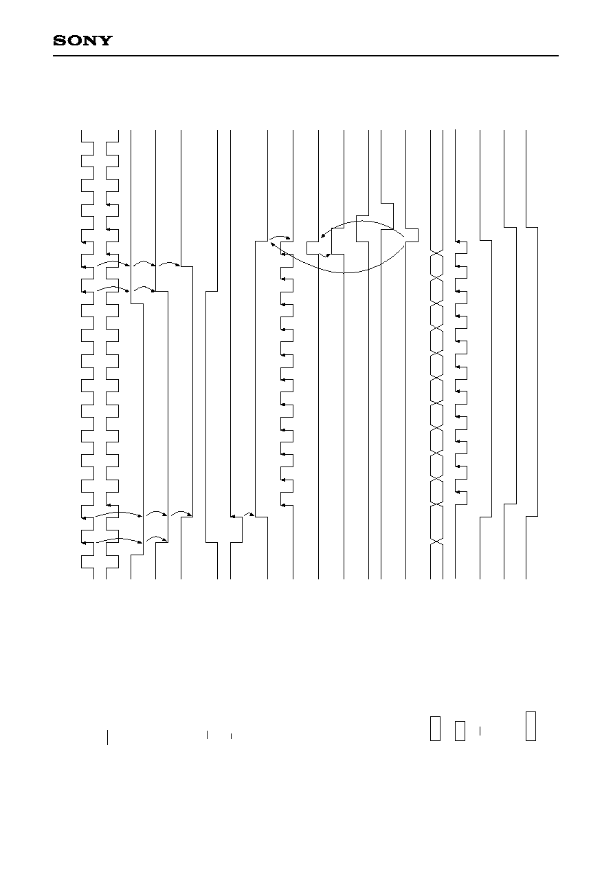
Circuit Diagram for 11-bit Serial Data Transfer Evaluation Tool
≠ 21 ≠
CXA1998BQ
Timing Chart for 11-bit Serial Data Transfer Evaluation Tool
D
u
m
m
y
D
1
D
2
D
3
D
4
D
5
D
6
D
7
D
8
D
9
D
1
0
D
1
1
2
µ
s
C
O
U
N
T
R
E
S
E
T
C
L
O
C
K
S
T
O
P
(
1
4
)
R
E
S
E
T
/
C
L
O
C
K
S
T
O
P
a
n
d
C
O
U
N
T
R
E
S
E
T
(
1
5
)
D
A
T
A
H
C
1
6
5
(
1
6
)
C
L
K
(
1
7
)
=
(
8
)
(
1
8
)
(
1
9
)
L
A
T
C
H
(
1
3
)
(
1
2
)
(
1
1
)
H
C
1
2
3
(
1
0
)
H
w
h
e
n
A
=
B
(
9
)
(
8
)
C
L
K
G
A
T
E
C
O
N
T
.
(
7
)
S
/
L
(
6
)
=
(
4
)
(
5
)
(
4
)
(
3
)
S
T
A
R
T
P
U
L
S
E
(
2
)
C
L
K
(
1
)
C
L
K
The numbers (1) to (19) correspond to those of test pins for the 11-bit serial data transfer evaluation tool circuit.
≠ 22 ≠
CXA1998BQ
Detection status
AMS OUT (Pin 12)
Signal detection
Low
No signal detection
High
PB OUT1
PB OUT2
2
0
k
2
0
k
SA
LPF
DET
25kHz
100k
GND
V
CC
V
CC
V
CC
GND
AMS GND
AMS OUT
AMS TC
C
1
R
1
R
2
C
2
R
3
HPF
AMS GAIN
Inside IC
9
11
12
10
f
C
G
10
1kHz
25kHz
100kHz
GAIN
(dB)
f (Hz)
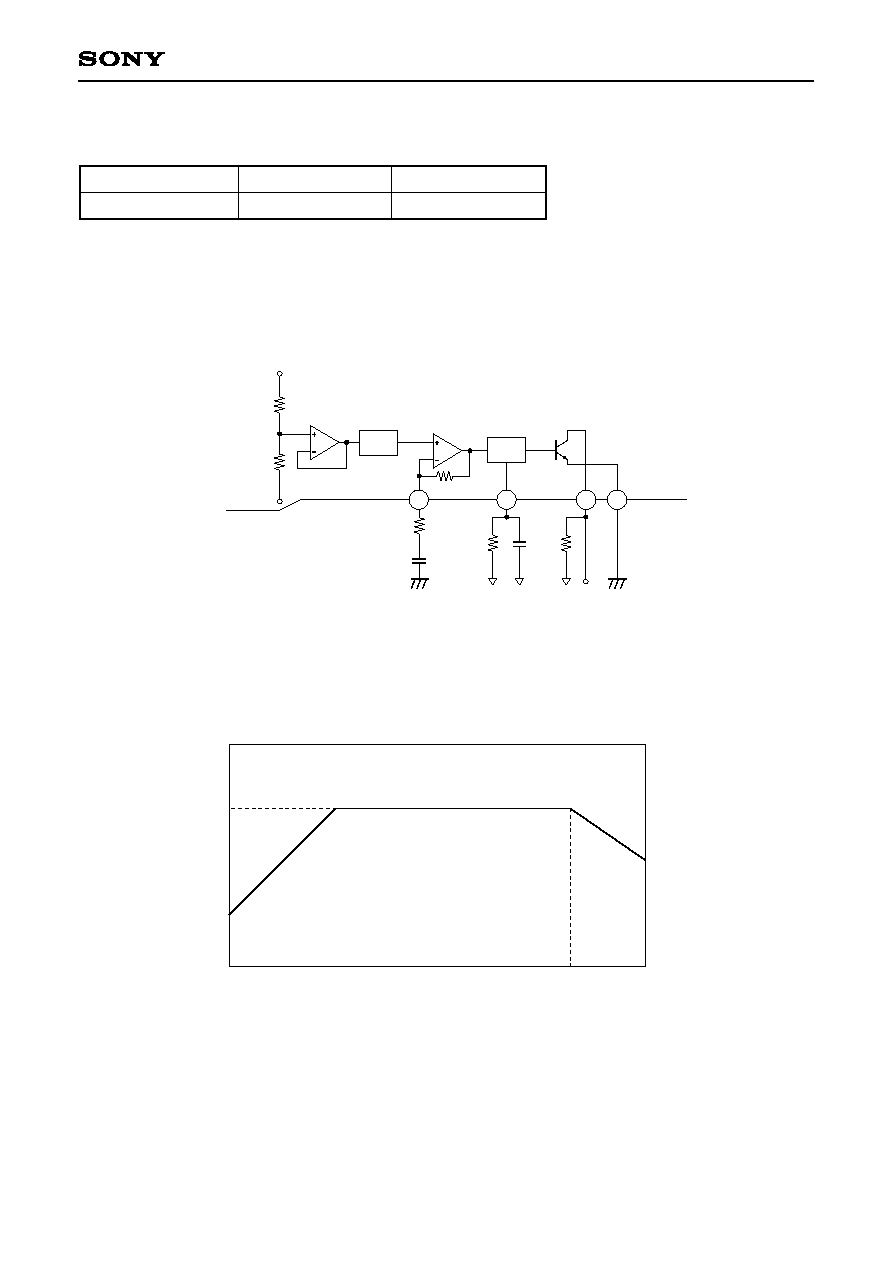
3. AMS
(1) AMS output logic
AMS OUT (Pin 12) is an open collector output pin. When a 3.9 k
resistor is connected to V
CC
= 8V:
Low: approximately 0.5V (I
OL
= 2mA (max.))
High: 8V
Fig. 1 shows the AMS block diagram.
Fig. 1. AMS Block Diagram
Fig. 2 shows the frequency response of the signal output from HPF.
Fig. 2. Frequency Response

≠ 23 ≠
CXA1998BQ
(2) AMS level setting
The AMS level is set by adjusting HPF gain and cut-off frequency with the external resistor and capacitor at
Pin 9.
G and fc in Fig. 2 are obtained from the following formula.
G = 20log (1 + 100k/R1) [dB] (1)
fc = 1 / (2 ∑
∑ C1 ∑ R1) [Hz]
Full-wave rectifier is applied for the signal at DET.
Signal detection time is set by the time constant of Pin 11 external resistor and capacitor.
DET signal detection level:
= ≠7.5dBm (typ.)
= playback equalizer reference output level + AMS level + HPF gain (2)
Playback equalizer reference output level of ≠21dBm is 0dB.
Ex.)
To set AMS level at ≠25dB, determine and set the constant for Pin 9 external resistor.
(Calculate assuming PBOUT1 = PBOUT2)
First, get the required HPF gain from formula (2).
≠7.5dBm = ≠21dBm + (≠25dB) + HPFgain,
so HPF gain = 38.5dB.
Next, get Pin 9 external resistance from formula (1).
38.5dB = 20log (1 + 100k / R1),
so R1
1.2k
,
and external resistance is 1.2k
.
≠ 24 ≠
CXA1998BQ
Example of Representative Characteristics
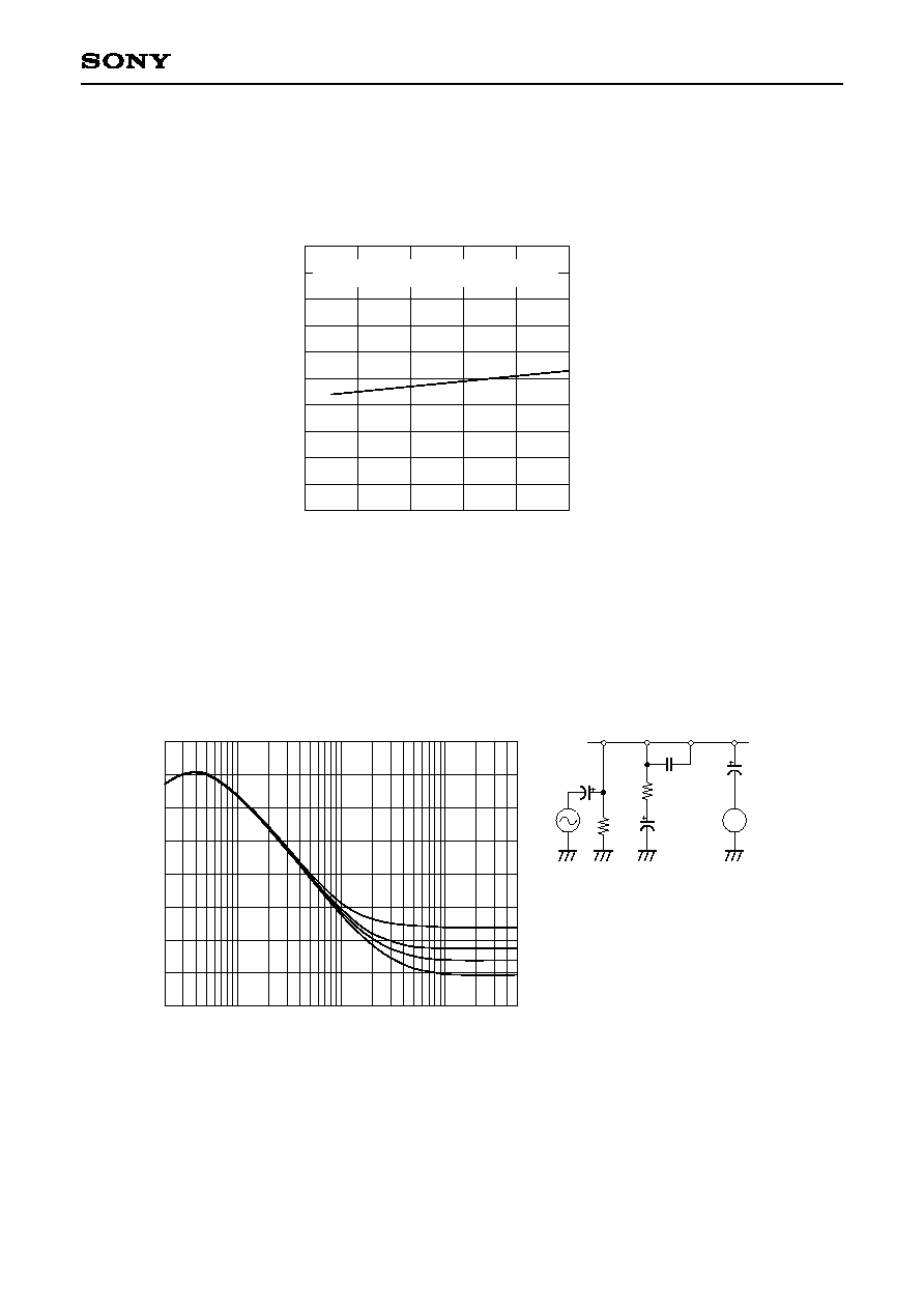
Quiescent current consumption vs.
Supply voltage
Vcc ≠ Supply voltage [V]
Q
u
i
e
s
c
e
n
t
c
u
r
r
e
n
t
c
o
n
s
u
m
p
t
i
o
n
[
m
A
]
6
15
11
7
8
9
10
25
16
17
18
19
20
21
22
23
24
Icc is the sum of the Vcc and V
DD
currents.
V
DD
= 5.0V
P
B
I
N
P
B
F
B
1
P
B
F
B
2
P
B
O
U
T
Playback equalizer frequency response
Frequency [Hz]
65
60
55
50
45
40
35
30
25
G
A
I
N
[
d
B
]
20
50
100 200
500
1k
2k
5k
10k 20k
50k
120µs ≠ NS
120µs ≠ HS
70µs ≠ NS
70µs ≠ HS
M
V
CC
= 8V
0.018µ
4
7
0
10µF
4
7
µ
1
0
0
2
.
2
µ

≠ 25 ≠
CXA1998BQ
Recording equalizer frequency response
Frequency [Hz]
O
u
t
p
u
t
r
e
s
p
o
n
s
e
[
d
B
]
20
0
100
50
200
1k
500
2k
10k
5k
20k
50k
2
4
6
8
10
12
14
16
18
20
22
24
26
Recording equalizer frequency response
Frequency [Hz]
O
u
t
p
u
t
r
e
s
p
o
n
s
e
[
d
B
]
20
100
50
200
1k
500
2k
10k
5k
20k
50k
V
CC
= 8V
0dB = NORM ≠ NS, 315Hz, ≠30dBm
≠2
≠4
0
2
4
6
8
10
12
14
16
18
20
22
24
26
≠2
≠4
V
CC
= 8V
0dB = NORM ≠ NS, 315Hz, ≠30dBm
(TAPE) (SPEED)
NORM ≠
HS
CrO
2
≠
HS
METAL≠
HS
(TAPE) (SPEED)
NORM ≠
HS
CrO
2
≠
HS
METAL≠
HS

≠ 26 ≠
CXA1998BQ
AMS quiescent detection level frequency response
Frequency [Hz]
30
25
20
15
10
5
0
≠5
≠10
≠15
≠20
≠25
≠30
≠35
≠40
A
M
S
i
n
p
u
t
l
e
v
e
l
(
p
l
a
y
b
a
c
k
e
q
u
a
l
i
z
e
r
o
u
t
p
u
t
l
e
v
e
l
)
[
d
B
]
20
50
100 200
500
1k
2k
5k
10k 20k
50k
V
CC
= 8V
120µs ≠ NS
AMS OUT 8V
0dB = ≠21dBm, 315Hz (playback equalizer reference output level)
A
B
A: Pin 9 R9.1k C0.015µ
B: Pin 9 R1k C0.1µ
A
M
S
G
A
I
N
A
M
S
T
C
A
M
S
O
U
T
0
.
1
µ
1
0
0
k
1
0
0
k
to 8V
A : 0.015µ 9.1k
B : 0.1µ 1k
9
11
12
AGC output characteristics
A
G
C
T
C
47µ
300k
V
CC
= 8V
1kHz
AGC OFF
AGC ON
10
5
0
≠5
≠10
≠15
≠35
≠30
≠25
≠20
≠15
≠10
≠5
Input level [dBm]
O
u
t
p
u
t
l
e
v
e
l
[
d
B
m
]
4
≠ 27 ≠
CXA1998BQ
Recording equalizer total harmonic distortion
Output level [dBm]
T
.
H
.
D
+
N
o
i
s
e
[
%
]
≠15
10
0
5
0.1
0.2
0.5
1.0
2.0
V
CC
= 8V
NORM ≠ NS
R
L
= 2.7k
1kHz
0dB = ≠10dBm
≠10
≠5
Playback equalizer total harmonic distortion
Output level [dBm]
T
.
H
.
D
+
N
o
i
s
e
[
%
]
≠30
≠5
≠15
≠10
0.1
0.2
0.5
1.0
2.0
V
CC
= 8V
120µs ≠ NS
R
L
= 2.7k
1kHz
≠25
≠20

≠ 28 ≠
CXA1998BQ
Package Outline
Unit: mm
SONY CODE
EIAJ CODE
JEDEC CODE
M
PACKAGE STRUCTURE
PACKAGE MATERIAL
LEAD TREATMENT
LEAD MATERIAL
PACKAGE WEIGHT
EPOXY RESIN
SOLDER / PALLADIUM
PLATING
COPPER / 42 ALLOY
48PIN QFP (PLASTIC)
15.3 ± 0.4
12.0 ≠ 0.1
+ 0.4
0.8
0.3 ≠ 0.1
+ 0.15
± 0.12
13
24
25
36
37
48
1
12
2.2 ≠ 0.15
+ 0.35
0
.
9
±
0
.
2
0.1 ≠ 0.1
+ 0.2
1
3
.
5
0.15
0.15 ≠ 0.05
+ 0.1
QFP-48P-L04
QFP048-P-1212-B
0.7g
NOTE : PALLADIUM PLATING
This product uses S-PdPPF (Sony Spec.-Palladium Pre-Plated Lead Frame).