 | –≠–ª–µ–∫—Ç—Ä–æ–Ω–Ω—ã–π –∫–æ–º–ø–æ–Ω–µ–Ω—Ç: CXA2019 | –°–∫–∞—á–∞—Ç—å:  PDF PDF  ZIP ZIP |
≠ 1 ≠
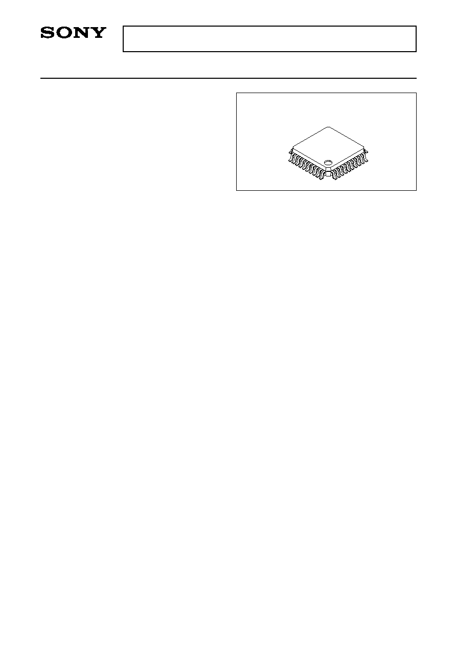
CXA2019AQ
40 pin QFP (Plastic)
E98320-PS
NTSC/PAL Chroma Decoder
Description
The CXA2019AQ is a bipolar IC which integrates
the luminance signal processing, chroma signal
processing,
and sync signal processing functions for
NTSC/PAL system color TVs onto a single chip.
Features
∑ Sub picture bright and white balance can be
adjusted by using the main picture Y/C/J BGP
output as the timing pulse
∑ I
2
C BUS compatible; two bus lines (SCL, SDA)
allow various adjustments and user controls
∑ Countdown system eliminates need for H and V
oscillator frequency adjustment
∑ Non-adjusting Y system filters (chroma trap, delay
line)
∑ Automatic identification of color system (forced
control possible)
∑ Automatic identification of 50/60Hz vertical frequency
(forced control possible)
∑ Built-in delay line aperture correction
∑ Built-in dynamic picture (black expansion) function
∑ Combination with a non-adjusting SECAM chroma
decoder allows configuration of multiple systems
Absolute Maximum Ratings
(Ta = 25∞C, SGND, JGND = 0V)
∑ Supply voltage
V
CC
12
V
∑ Operating temperature
Topr ≠20 to +75
∞C
∑ Storage temperature
Tstg ≠65 to +150 ∞C
∑ Allowable power dissipation P
D
1.67
W
Operating Conditions
Supply voltage
V
CC
9 ± 0.5
V
Applications
Color TVs
Structure
Bipolar silicon monolithic IC
Sony reserves the right to change products and specifications without prior notice. This information does not convey any license by
any implication or otherwise under any patents or other right. Application circuits shown, if any, are typical examples illustrating the
operation of the devices. Sony cannot assume responsibility for any problems arising out of the use of these circuits.

≠ 2 ≠
CXA2019AQ
Block Diagram
1
2
4
5
6
7
8
9
1
0
1
1
1
2
1
3
1
4
1
5
1
6
1
7
1
8
1
9
2
0
2
1
2
2
2
3
2
4
2
5
2
6
2
7
2
8
2
9
3
0
4
0
3
9
3
8
3
7
3
6
3
5
3
4
3
1
3
2
3
3
V
O
U
T
U
O
U
T
Y
O
U
T
S
G
N
D
2
SC
P
H T
IM
V T
IM
V
2
I
N
U
2
I
N
Y
2
I
N
S
G
N
D
C
I
N
A P
ED
C
V
B
S
/
Y
I
N
AD
RS
SC
L
SD
A
V S
YN
C
H S
YN
C
V H
OL
D
SE
CA
M R
EF
AP
C
X 4
43
/3
58
X 3
58
X N
TS
C
SV
CC
≠ (
R_
Y)
OU
T
≠ (
B_
Y)
OU
T
≠ (
B_
Y)
IN
≠ (
R_
Y)
IN
CE
RA
AF
C
IR
EF
J G
ND
V2
O
UT
U2
O
UT
Y2
O
UT
A
B
L
F
I
L
I
N
C
P
I
N
T
h
e
s
u
b
p
i
c
t
u
r
e
b
r
i
g
h
t
a
n
d
w
h
i
t
e
b
a
l
a
n
c
e
c
a
n
b
e
a
d
j
u
s
t
e
d
b
y
r
e
c
e
i
v
i
n
g
B
G
P
o
r
S
C
P
o
u
t
p
u
t
f
r
o
m
t
h
e
m
a
i
n
p
i
c
t
u
r
e
Y
/
C
/
J
,
c
l
a
m
p
i
n
g
t
h
e
P
I
N
P
P
R
O
C
.
o
u
t
p
u
t
,
a
n
d
v
a
r
y
i
n
g
t
h
e
D
C
o
f
t
h
e
c
l
a
m
p
e
d
p
o
r
t
i
o
n
.
I
2
C
B
U
S
D
E
C
O
R
D
E
R
I
R
E
F
H
.
S
Y
N
C
S
E
P
P
H
A
S
E
D
E
T
.
1
/
3
2
H
.
D
R
I
V
E
3
2
f
H
V
C
O
V
.
S
Y
N
C
S
E
P
V
C
O
U
N
T
D
O
W
N
V
2
P
E
D
V
2
D
R
I
V
E
U
2
P
E
D
U
2
D
R
I
V
E
Y
2
D
R
I
V
E
A
B
L
Y
D
R
I
V
E
U
P
E
D
V
P
E
D
A
U
T
O
P
E
D
E
S
T
A
L
C
L
A
M
P
D
E
L
A
Y
S
H
A
R
P
N
E
S
S
T
R
A
P
T
R
A
P
S
U
B
C
O
N
T
V
I
D
E
O
S
W
B
S
T
A
M
P
C
O
L
O
R
K
I
L
L
E
R
P
H
A
S
E
D
E
T
.
H
U
E
L
P
F
S
E
C
A
M
C
H
R
O
M
A
V
C
O
4
.
4
3
/
3
.
5
8
S
W
N
T
/
P
A
L
P
A
L
I
D
I
D
A
X
I
S
F
.
F
D
E
M
A
X
I
S
P
H
A
S
E
S
H
I
F
T
C
H
R
O
M
A
D
E
T
.
D
E
T
S
W
C
O
L
O
R
C
L
A
M
P
A
C
C
D
E
T
.
A
C
C
D
E
L
A
Y
T
O
T
A
B
L
C
E
N
T
Y
2
D
R
I
V
E
U
2
D
R
I
V
E
U
2
P
E
D
V
2
D
R
I
V
E
V
2
P
E
D
5
0
/
6
0
C
M
O
D
E
A
F
C
H
L
O
C
K
2
f
H
V
P
E
D
U
P
E
D
Y
D
R
I
V
E
D
C
T
R
A
N
S
H
A
R
P
N
E
S
S
S
H
P
f
0
P
R
E
O
V
E
R
D
E
L
A
Y
T
R
A
P
O
N
S
E
C
A
M
S
U
B
C
O
N
T
C
V
/
Y
C
C
O
L
O
R
N
T
/
P
A
L
E
X
T
C
O
L
O
R
2
f
H
N
T
/
P
A
L
H
U
E
S
U
B
H
U
E
X
'
T
A
L
P
I
N
K
I
L
L
E
R
T
O
T
O
N
S
U
B
C
O
L
O
R
3
J V
cc

≠ 3 ≠
CXA2019AQ
Pin Configuration
1
2
3
4
5
6
7
8
9
10
11
12
13
14
15
16
17
18
19
20
21
22
23
24
25
26
27
28
29
30
40
39
38
37
36
35
34
31
32
33
V OUT
U OUT
Y OUT
SGND2
SCP
H TIM
V TIM
V2 IN
U2 IN
Y2 IN
S GND
CIN
A PED
CVBS/Y IN
ADRS
SCL
SDA
V SYNC
H SYNC
V HOLD
S
E
C
A
M
R
E
F
A
P
C
X
4
4
3
/
3
5
8
X
3
5
8
X
N
T
S
C
S
V
C
C
≠
(
R
_
Y
)
O
U
T
≠
(
B
_
Y
)
O
U
T
≠
(
B
_
Y
)
I
N
≠
(
R
_
Y
)
I
N
C
E
R
A
A
F
C
J
V
C
C
I
R
E
F
J
G
N
D
V
2
O
U
T
U
2
O
U
T
Y
2
O
U
T
A
B
L
F
I
L
I
N
C
P
I
N
≠ 4 ≠
CXA2019AQ
32f
H
(500 or 503.5kHz) ceramic
oscillator connection.
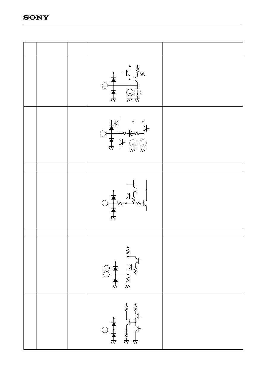
Pin Description
Pin
No.
Symbol
Equivalent circuit
Description
1
CERA
2
AFC
CR connection for AFC lag-lead filter.
4
IREF
Connect a 10k
resistor between this
pin and GND.
6
7
V2 OUT
U2 OUT
Reinput system outputs.
8
Y2 OUT
Reinput system output.
3
JV
CC
5
--
--
1.8V
3V
3V
9.0V
--
J GND
Power supply.
Jungle system (H/V) GND.
Vcc
Vcc
10k
28k
Vcc
1
46k
Vcc
2
1.2k
Vcc
Vcc
14.4k
Vcc
150
4
20k
8.6k
Vcc
20k
Vcc
200
7
6
8k
Vcc
4k
Vcc
200
Vcc
8
Pin
voltage
≠ 5 ≠
CXA2019AQ
Reinput system clamp pulse input.
Input the main picture BGP (SCP).
Vth: 2.5V
Pin
No.
Symbol
Equivalent circuit
Description
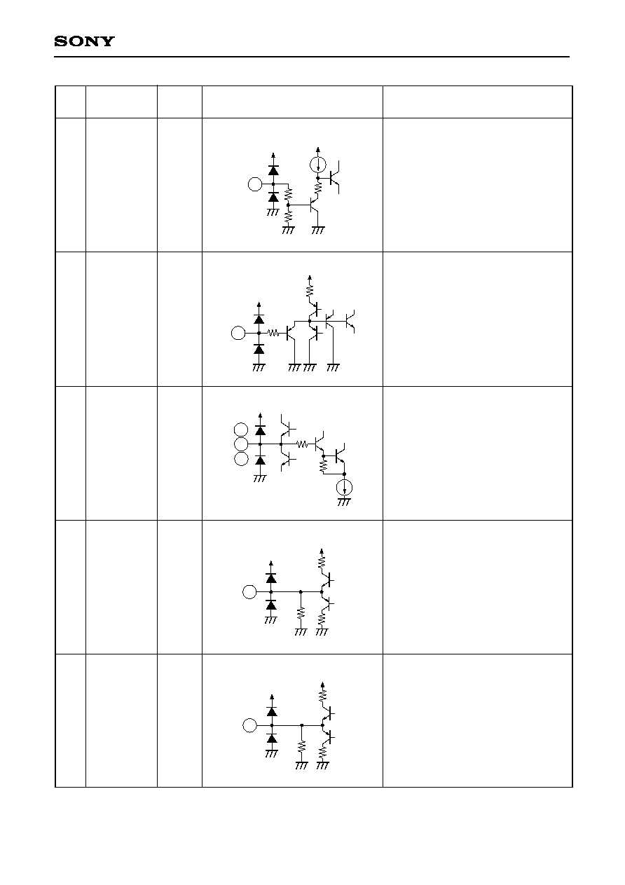
9
ABLFILIN
ABLFIL voltage input.
Input the main picture Y/C/J ABLFIL
voltage.
10
CP IN
11
12
13
Y2 IN
U2 IN
V2 IN
Reinput system inputs.
Input via a capacitor.
14
V TIM
V timing pulse output.
Outputs a 0 to 5V positive polarity
pulse.
37k
Vcc
90k
Vcc
90k
9
Vcc
1.2k
Vcc
15k
10
11
13
1.2k
Vcc
70k
12
20k
Vcc
Vcc
1k
14
1k
15
--
--
4V
--
--
H TIM
H timing pulse output.
Outputs a 0 to 5V positive polarity
pulse.
20k
Vcc
Vcc
1k
1k
15
Pin
voltage

≠ 6 ≠
CXA2019AQ
GND.
Pin
No.
Symbol
Equivalent circuit
Description
16
SCP
Outputs BGP and HBLK as SCP
(sand castle pulse).
The typ. waveform is as follows.
Vcc
Vcc
1.2k
Vcc
500µA
16
18
Y OUT
Y (luminance signal) output.
Standard output level: 1.1Vp-p
6k
Vcc
20k
Vcc
200
18
19
20
U OUT
V OUT
U/V (color difference signal) outputs.
Output level: U = V = 1.2Vp-p
(In case of setting data as shown in
"I
2
C BUS Register Initial Settings.")
19
8.6k
Vcc
20k
Vcc
200
20
21
22
≠ (R_Y) IN
≠ (B_Y) IN
Color difference signal inputs. Input
as negative polarity via a capacitor.
Standard input levels:
B-Y: 1.33Vp-p
R-Y: 1.05Vp-p
21
Vcc
1.2k
Vcc
70k
22
100µA
BGP
17
--
3V
3V
5.6V
--
SGND2
Pin
voltage
HBLK
BGP
5.0V
2.0V
0.3V

≠ 7 ≠
CXA2019AQ
Power supply.
Pin
No.
Symbol
Equivalent circuit
Description
23
24
≠ (B_Y) OUT
≠ (R_Y) OUT
Color difference signal outputs.
Output as negative polarity.
Standard output levels:
B-Y: 0.665Vp-p
R-Y: 0.525Vp-p
23
Vcc Vcc
Vcc
24
1.2k
26
27
28
X NTSC
X 358
X443/358
Crystal oscillator connections.
Connect the PALN and 4.43MHz
crystal to Pin 28.
Connect the PALM crystal to Pin 27,
and the NTSC crystal to Pin 26.
26
28
Vcc
Vcc
4k
500
27
29
APC
CR connection for APC lag-lead filter.
Vcc
1.2k
Vcc
1.2k
25k
29
30
SECAM REF
When the IC is set to SECAM
identification mode, the 4.43MHz VCO
oscillator waveform is output from this
pin centering on DC 1.5V.
If a 150µA current is led from this pin
during this identification mode, the IC
is set to SECAM mode. In SECAM
mode, the 4.43MHz VCO oscillator
waveform is output centering on
DC = 5V only during the VBLK
interval.
Vcc
40k
6k
Vcc
Vcc
10p
30
25
SV
CC
Pin
voltage
31
5.6V
--
--
1.5V
9.0V
--
S GND
GND.

≠ 8 ≠
CXA2019AQ
This pin is used to switch the slave
address.
Vcc: 9AH
GND: 9EH
Vth = 2.5 V
35
Pin
No.
Symbol
Equivalent circuit
Description
32
C IN
Chroma signal input.
Standard input level (burst level)
: 570mVp-p
33
A PED
Black peak hold for auto pedestal (black
expansion). Connect a capacitor.
Vcc
30k
10p
32
30k
Vcc
1.2k
Vcc
16k
20k
20k
Vcc
Vcc
33
34
--
--
--
--
CVBS/Y IN
Y signal input. Input via a capacitor.
Standard input level: 2Vp-p
Vcc
1.2k
1.2k
1.2k
70k
34
Vcc
ADRS
35
Vcc
30k
77k
Pin
voltage

≠ 9 ≠
CXA2019AQ
V sync separation input. Input a 2Vp-p
video signal via a capacitor and
resistor.
V HOLD
Pin
No.
Symbol
Equivalent circuit
Description
36
37
SCL
SDA
I
2
C BUS SCL (Serial Clock) and SDA
(Serial Data).
Vilmax = 1.5V
Vihmin = 3V
Volmax = 0.4V
38
V SYNC
36
4k
4k
Vcc
37
Vcc
15k
20µA
150
38
24k
33k
39
H SYNC
H sync separation input. Input a 2Vp-p
video signal via a capacitor and
resistor.
Vcc
14k
10µA
150
24k
20k
39
40
--
3.5V
2.5V
--
Peak hold for V sync separation.
Connect a capacitor.
Vcc
50k
1k
150
55k
40
Pin
voltage

≠ 10 ≠
CXA2019AQ
1
2
3
4
5
6
7
8
9
10
11
I
CC
f
H
f
H
HTIM-W
HTIM-H
HTIM-L
SBLK-W
SBGP-W
t1
t2
t3
94
15.85
400
10.4
5.1
0.5
11.2
4.3
46
15.50
≠400
9.3
4.5
0.0
9.6
3.2
Measure the pin inflow current.
HTIM output frequency
Confirm that I
2
C bus register HLOCK is 1
(the pull-in range when f
H
is shifted from
15.734kHz).
SV
CC
= JV
CC
= 9V
AFC: 0
SCP BGR: 1
SCP BGF: 1
AFC: 0
SYNCIN: SIG-H3/SIG-H4
AFC: 1
SYNCIN: SIG-H3/SIG-H4
AFC: 2
SYNCIN: SIG-H3/SIG-H4
Current consumption
Horizontal free-running
frequency
Horizontal sync pull-in
range
HTIM output pulse
width
HTIM output high level
HTIM output low level
SCP BLK output pulse
width
SCP BGP output pulse
width
AFC gain 1
AFC gain 2
AFC gain 3
3, 25
15
15
15
16
15
mA
kHz
Hz
µ
s
V
V
µ
s
µ
s
µ
s
µ
s
µ
s
No.
Item
Symbol
Measurement conditions
Measure- ment pins
Measurement contents
Min.
Typ.
Max.
Unit
H system items
H
T
I
M
-
W
H
T
I
M
-
H
H
T
I
M
-
L
S
B
G
P
-
W
S
B
L
K
-
W
t
S
I
G
-
H
3
,
H
4
Electrical Characteristics
Setting conditions
∑
Ta = 25
∞
C, SV
CC
= JV
CC
= 9V
∑
Measures the following after setting the I
2
C bus register as shown in "I
2
C BUS Register Initial Settings".
68
15.65
9.9
4.85
0.1
10.5
3.8
0.4
0.6
1.2
t = t (SIG-H3) ≠ t (SIG-H4)
≠ 11 ≠
CXA2019AQ
12
13
14
15
16
17
18
19
20
21
22
23
24
25
fV1
VTIM-H
VTIM-L
fV2
Vc1amp
Vped1
Vped2
Vrc1amp
Vrped1
Vrped2
65
5.3
0.5
55
3.2
16
≠4
3.2
57
≠13
55
4.7
0.0
45
2.7
5
≠15
2.7
32
≠41
VFREQ: 0
VFREQ: 1
U PED: 1F
V PED: 1F
U PED: 0
V PED: 0
CP IN: SIG-H5 (Normally input
when reinput system is measured)
U2 PED: 1F
V2 PED: 1F
U2 PED: 0
V2 PED: 0
Vertical free-running
frequency 1
VTIM output high level
VTIM output low level
Vertical free-running
frequency 2
U/VOUT clamp
U/VOUT pedestal
variation 1
U/VOUT pedestal
variation 2
U2/V2OUT clamp
U2/V2OUT pedestal
variation 1
U2/V2OUT pedestal
variation 2
Y2 DRIVE variable
range 1
Y2 DRIVE variable
range 2
U2/V2 DRIVE variation 1
U2/V2 DRIVE variation 2
14
14
14
14
19
20
6
7
Hz
V
V
Hz
V
mV
mV
V
mV
mV
dB
dB
dB
dB
No.
Item
Symbol
Measurement conditions
Measure- ment pins
Measurement contents
Min.
Typ.
Max.
Unit
V system items
V
T
I
M
-
H
V
T
I
M
-
L
V
c
l
a
m
p
V
p
e
d
.
1
,
2
H
T
I
M
U
/
V
O
U
T
V
r
c
l
a
m
p
V
r
p
e
d
.
1
,
2
S
I
G
-
H
5
U
2
/
V
2
O
U
T
60
5.0
0.2
50
3.0
10
≠8
3.0
45
≠27
YUV system items
Gy2dr = 20 log
Grdr = 20 log
Vx (Y2 DRIVE: 1F/0)
Vx (Y2 DRIVE: F)
Gy2dr1
Gy2dr2
Grdr1
Grdr2
3.3
≠3.3
4.4
≠4.5
2.3
≠4.9
2.8
≠8.0
Y2 IN: SIG-Y1
Y2 DRIVE: 1F
Y2 IN: SIG-Y1
Y2 DRIVE: 0
U2/V2 IN: SIG-Y1
U2 DRIVE: 1F
V2 DRIVE: 1F
U2/V2 IN: SIG-Y1
U2 DRIVE: 0
V2 DRIVE: 0
8
6
7
V
x
V
x
2.8
≠4.0
3.6
≠6.3
Vx (U2/V2 DRIVE: 1F/0)
Vx (U2/V2 DRIVE: F)
VTIM output frequency (for 60Hz mode)
VTIM output frequency (for 50Hz mode)
≠ 12 ≠
CXA2019AQ
Vyout = V
x
(Y DRIVE: F)
Gydr1, 2 = 20 log
Gshr1, 2 = 20 log
Gsc1, 2 = 20 log
26
27
28
29
30
31
32
33
Vyout
Gydr1
Gydr2
Gshr
Gshr1
Gshr2
Gsc1
Gsc2
1.3
4.2
≠5.7
4.2
8.3
≠4.1
2.9
≠2.7
0.9
2.8
≠6.9
2.8
6.8
≠6.3
1.9
≠3.5
Y IN: SIG-Y2
Y DRIVE: F
Y IN: SIG-Y2
Y DRIVE: 1F
Y IN: SIG-Y2
Y DRIVE: 0
Y IN: SIG-Y3
SHARPNESS: 7
Y IN: SIG-Y3
SHARPNESS: F
Y IN: SIG-Y3
SHARPNESS: 0
Y IN: SIG-Y2
SUB CONT: F
Y IN: SIG-Y2
SUB CONT: 0
Y OUT output
amplitude
Y DRIVE variable
range 1
Y DRIVE variable
range 2
SHARPNESS center
SHARPNESS variable
range 1
SHARPNESS variable
range 2
SUB CONT variable
range 1
SUB CONT variable
range 2
Y OUT frequency
response
C-TRAP attenuation
358
C-TRAP attenuation
443
18
18
18
V
dB
dB
dB
dB
dB
dB
dB
No.
Item
Symbol
Measurement conditions
Measure- ment pin
Measurement contents
Min.
Typ.
Max.
Unit
Y system items
V
x
1.1
3.5
≠6.3
3.5
7.6
≠5.2
2.4
≠3.1
Vx (Y DRIVE: 1F/0)
Vx (Y DRIVE: F)
Vx (f = 3MHz)
Vx (f = 100kHz)
Vx (SUB CONT: F/0)
Vx (SUB CONT: 7)
V
x
V
x
fyout = 20 log
C-trap = 20 log
Vx (f = 8MHz)
Vx (f = 100kHz)
34
35
36
fyout
C-trap1
C-trap2
2.2
≠25
≠25
≠3.0
Y IN: SIG-Y4
Y IN: SIG-Y5
TRAP SW: 0/1
CTRAPADJ: adjustment value
Y IN: SIG-Y6
TRAP SW: 0/1
CTRAPADJ: adjustment value
18
18
18
dB
dB
dB
V
x
V
x
≠0.5
≠35
≠35
Vx (TRAP SW: 1)
Vx (TRAP SW: 0)
≠ 13 ≠
CXA2019AQ
Gcol1, 2 = 20 log
Gscol1, 2 = 20 log
Confirm that the burst frequency is pulled in
at 3.58MHz
±
400Hz.
37
38
39
40
41
42
43
44
45
Vuout
Vvout
Gcol1
Gcol2
Gscol1
Gscol2
offset
KP
fAPC
1.5
1.5
6.8
10
3.3
≠2.3
5
400
0.9
0.9
5.8
2.1
≠5.0
≠11
≠400
C IN: SIG-C1 (No.37 to 42)
C IN: SIG-C2 (No.37 to 42)
COLOR: 3F
COLOR: 0
SUB COLOR: F
SUB COLOR: 0
CVBS: burst only
During NTSC input
UOUT output amplitude
VOUT output amplitude
COLOR variable range 1
COLOR variable range 2
SUB COLOR variable
range 1
SUB COLOR variable
range 2
HUE center offset
Killer point
APC pull-in range
19
20
19
20
19
20
--
--
--
V
V
dB
mV
dB
dB
deg
dB
Hz
No.
Item
Symbol
Measurement conditions
Measure- ment pin
Measurement contents
Min.
Typ.
Max.
Unit
1.2
1.2
6.3
2.7
≠3.6
≠3
≠33
C system items
V
x
Vx (COLOR: 3F/0)
Vx (COLOR: 1F)
Vx (SUB COLOR: F/0)
Vx (SUB COLOR: 7)
V
x

≠ 14 ≠
CXA2019AQ
No.
Item
Symbol
Min.
Typ.
Max.
Unit
46
47
48
49
50
51
52
53
54
55
56
57
58
59
60
61
62
63
High level input voltage
Low level input voltage
High level input current
Low level input current
Low level output voltage
During current inflow of 3 mA to SDA
(Pin 37)
SDA inflow current
Input capacitance
Clock frequency
Minimum waiting time for data change
Waiting time for data transfer start
Low level clock pulse width
High level clock pulse width
Waiting time for start preparation
Data hold time
Data preparation time
Rise time
Fall time
Waiting time for stop preparation
Vih
Vil
lih
lil
Vol
lol
Ci
fscl
tbuf
thd;sta
tlow
thigh
tsu;sta
thd;dat
tsu;dat
tr
tf
tsu;sto
3.0
0
--
--
0
3
--
0
4.7
4.0
4.7
4.0
4.7
0
250
--
--
4.7
--
--
--
--
--
--
--
--
--
--
--
--
--
--
--
--
--
--
5.0
1.5
10
10
0.4
--
10
100
--
--
--
--
--
--
--
300
300
--
V
V
µA
µA
V
mA
pF
kHz
µs
µs
µs
µs
µs
µs
ns
ns
ns
µs
I
2
C BUS System Items

≠ 15 ≠
CXA2019AQ
Electrical Characteristics Measurement Circuit
1µ
100
4700p
220
0.47µ
330k
2.2k
3.3k
100p
SYNCIN
100
100
I
2
C bus
input/output
4.7µ
9V or 0V
0.47µ
YIN
Composite
video input
CIN
330
500kHz
ceramic
oscillator
0.01µ
8.2k
1µ
9V
0.01µ
47µ
10k
V2
output
U2
output
Y2
output
CPIN
ABL
voltage
NTSC
9V
Y2 IN
1µ
U2 IN
1µ
V2 IN
1µ
V TIM output
H TIM output
SCP output
Y output
U output
V output
1µ
1µ
47µ
0.01µ
15p
1.5k
15p
1.5k
15p
470
470p
0.47µ
15k
PAL/M
PAL
S
E
C
A
M
R
E
F
A
P
C
21
22
23
24
25
26
27
28
29
30
X
4
4
3
/
3
5
8
X
3
5
8
X
N
T
S
C
S
V
C
C
≠
(
R
_
Y
)
O
U
T
≠
(
B
_
Y
)
O
U
T
≠
(
B
_
Y
)
I
N
≠
(
R
_
Y
)
I
N
2
3
4
5
6
7
8
9
10
1
C
E
R
A
A
F
C
J
V
C
C
J
G
N
D
V
2
O
U
T
U
2
O
U
T
C
P
I
N
A
B
L
F
I
L
I
N
Y
2
O
U
T
I
R
E
F
11
12
13
14
15
16
17
18
19
20
Y2 IN
U2 IN
V TIM
H TIM
SCP
Y OUT
V OUT
V2 IN
SGND2
U OUT
40
39
38
37
36
35
34
31
32
33
V HOLD
H SYNC
V SYNC
SDA
CIN
SCL
CVBS/Y IN
A PED
S GND
ADRS

≠ 16 ≠
CXA2019AQ
Application Circuit
1µ
100
4700p
220
0.47µ
330k
2.2k
3.3k
100p
100
100
I
2
C bus
input/output
4.7µ
0.47µ
Composite
video input
330
500kHz
ceramic
oscillator
0.01µ
8.2k
1µ
0.01µ
47µ
10k
V2
output
U2
output
Y2
otuput
ABL
input
NTSC
1µ
1µ
1µ
V TIM output
H TIM output
SCP output
Y output
U output
V output
1µ
1µ
47µ
15p
1.5k
15p
1.5k
15p
470p
0.47µ
15k
PAL/M
PAL/N
or PAL
Y2 input
U2 input
V2 input
Color difference
input from1H
delay line
Color difference
output to 1H
delay line
0.01µ
1.5k
*
1
S
E
C
A
M
R
E
F
A
P
C
21
22
23
24
25
26
27
28
29
30
X
4
4
3
/
3
5
8
X
3
5
8
X
N
T
S
C
S
V
C
C
≠
(
R
_
Y
)
O
U
T
≠
(
B
_
Y
)
O
U
T
≠
(
B
_
Y
)
I
N
≠
(
R
_
Y
)
I
N
2
3
4
5
6
7
8
9
10
1
C
E
R
A
A
F
C
J
V
C
C
J
G
N
D
V
2
O
U
T
U
2
O
U
T
C
P
I
N
A
B
L
F
I
L
I
N
Y
2
O
U
T
I
R
E
F
11
12
13
14
15
16
17
18
19
20
Y2 IN
U2 IN
V TIM
H TIM
SCP
Y OUT
V OUT
V2 IN
SGND2
U OUT
40
39
38
37
36
35
34
31
32
33
V HOLD
H SYNC
V SYNC
SDA
CIN
SCL
CVBS/Y IN
A PED
S GND
ADRS
+9V
CPIN
A2025
ABLFIL voltage input.
Connect to V
CC
when
not used.
*
1
: 470
when 4.43MHz crystal is used.
Application circuits shown are typical examples illustrating the operation of the devices. Sony cannot assume responsibility for
any problems arising out of the use of these circuits or for any infringement of third party patent and other right due to same.
≠ 17 ≠
CXA2019AQ
Signals Used for Measurements
4.7µs
0.57V
63.556µs
SIG-H1
f
H
= 15.734kHz
NTSC
4.7µs
0.57V
64.0µs
SIG-H2
f
H
= 15.625kHz
PAL
4.63µs
0.57V
62.563µs
SIG-H3
f
H
+ 250Hz
4.78µs
0.57V
64.583µs
SIG-H4
f
H
≠ 250Hz
3µs
3V
63.556µs
SIG-H5
4.8µs
SIG-Y1
SIG-Y2
0.57V
1.43V
1.0V
≠ 18 ≠
CXA2019AQ
0.7V
SIG-Y3
f = 3.0MHz or
100kHz
0.7V
SIG-Y4
f = 8.0MHz or
100kHz
0.7V
SIG-Y5
f = 3.58MHz
burst = 3.58MHz
0.57Vp-p
SIG-Y6: f = 4.43MHz, burst = 4.43MHz for SIG-Y5 signal
0.48Vp-p
SIG-C1
0.57V
180∞
168∞
348∞
0.68Vp-p
SIG-C2
0.57V
180∞
104∞
274∞
f = 3.58MHz
burst = 3.58MHz
f = 3.58MHz
burst = 3.58MHz

≠ 19 ≠
CXA2019AQ
Description of Operation
1. Sync System
The video signals (standard input level: 2Vp-p) input to Pins 38 and 39 are sync separated by the horizontal
and vertical sync separation circuits.
The resulting horizontal sync signal and the signal obtained by frequency dividing the 32f
H
-VCO output
using the ceramic oscillator (frequency 500kHz or 503.5kHz) by 32 are phase compared, the AFC loop is
constructed, and an H pulse (HTIM) synchronized with the H sync is output from Pin 15.
The vertical sync signal is sent to the V countdown block where the most appropriate window processing is
performed to obtain V sync timing information which resets the counter. A V pulse (VTIM) synchronized
with the V sync is output from Pin 14. In addition, BGP, HBLK and VBLK are output from Pin 16 as SCP
(sand castle pulse).
2. Y System
There are two input systems.
Composite video input (2Vp-p)
1 system
Y/C separation input (2Vp-p)
1 system
The Y signal (specified input level: 2Vp-p) input to Pin 34 passes through the subcontrast control, chroma
trap, delay line, sharpness control, clamp and auto pedestal circuits, is gain adjusted by the YDRIVE circuit
and is then output.
The CXA2019AQ has a built-in chroma trap, enabling the video signal to be input directly. The trap
frequency is automatically adjusted inside the IC. However, the trap frequency is affected by variations
among the ICs, so fine adjustment through the I
2
C bus may be required.
Because the f0 of the filter is not specified when the color killer function is operating, turn the trap OFF if
there are any difficulties.
The Y signal delay time can be varied in approximately 60ns increments through the I
2
C bus register
(DELAY). In addition, when the C system TOT is ON, the Y signal delay time is increased by approximately
140ns to cope with the increase in the C system delay time caused by the TOT filter.
The sharpness control is a delay line type and the sharpness f0 can be switched to 1.5MHz or 3MHz.
3. C System
The CVBS or chroma signal (specified input level: burst level of 570mVp-p) selected by the internal video
switch passes through the ACC, TOT, chroma amplifier and demodulation circuits, is demodulated into the
R-Y and B-Y color difference signals, and is then inversed and output from Pins 23 and 24. However,
during NTSC the signals are 6dB amplified by the internal DET switch and gain adjusted by the COLOR
circuit. During PAL the signals are 6dB amplified by the 1H delay line, input to Pins 21 and 22, and gain
adjusted by the COLOR circuit. Signals that have passed through the 1H delay line can also be input to the
COLOR circuit during NTSC by using the I
2
C bus register (EXT COLOR). This provides comb filter effects.
In addition, the color system (NTSC/PAL) and the subcarrier frequency (3.58MHz/4.43MHz) are
automatically identified according to the input chroma signal, and the internal VCO and demodulation
circuit, etc., are adjusted automatically. Furthermore, SECAM signals can also be automatically identified
by connecting an external SECAM decoder to Pin 30. In this case, Pins 23 and 24 and the SECAM decoder
color difference output are linked together directly, and one side goes to high impedance and the other side
goes to low impedance according to the input chroma signal, and then they are input to the external 1H
delay line.
System identification can be set to automatic or forced mode by the I
2
C bus register. The color system is
output to the status register.
The pedestal levels of the U and V color difference signals are clamped by UPED and VPED, respectively,
and then these signals are output. However, the DC of the video portion can be controlled by the I
2
C bus
register, allowing the offset to be adjusted at the PINP processor input.

≠ 20 ≠
CXA2019AQ
4. YUV Reinput System
The U and V color difference signals (output from the PINP processor) input to Pins 12 and 13 are clamped
according to the pulse input to Pin 10, gain controlled by the U2 and V2 drive circuits, the DC of their video
portion is controlled by the U2PED and V2PED circuits, and then these signals are output from Pins 6 and 7.
This function allows adjustment of the white balance and black level of the PINP sub picture.
In addition, the Y signal input to Pin 11 is clamped in the same manner, gain controlled by the Y2 drive
circuit, and output from Pin 8. At this time, bright ABL with a polarity opposite that of the main picture ABL
can be applied by inputting the main picture Y/C/J IC ABLFIL voltage to Pin 9. This allows fluctuation of the
black level of the sub picture caused by the main picture ABL to be suppressed. This reverse polarity ABL
can be turned ON and OFF and the gain and control curve center values can be set by the I
2
C bus register.
Notes on Operation
∑ The CXA2019AQ does not perform the initial settings during power ON. This initial data should be input from
a microcomputer.
∑ Because the YUV signal output from the CXA2019AQ are DC direct connected, the board pattern must be
designed consideration given to minimizing interference from around the power supply and GND.
Do not separate the GND patterns for each pin; a solid earth is ideal. Locate the power supply side of the
bypass capacitor which is inserted between the power supply and GND as near to the pin as possible. Also,
locate the XTAL oscillator, ceramic oscillator and IREF resistor as near to the pin as possible, and do not wire
signal lines near this pin.
∑ Use lead type (HC-49/U type) for each XTAL oscillator. Confirm that there is no problem for capture range
color response and others at resistors and capacitors as shown in Application Circuit.
∑ Murata's Ceralock is recommended for ceramic oscillator. When using only for NTSC, 503.5kHz Ceralock; for
NTSC/PAL, 500kHz Ceralock is recommended.
∑ Use a resistor (such as a metal film resistor) with an error of less than 1% for the IREF pin.
∑ For unused pins, leave them open.
≠ 21 ≠
CXA2019AQ
TOT ON
CD MODE2
SHARPNESS
SUB HUE
CTRAPADJ
U PED
U2 PED
Definition of I
2
C BUS Registers
Slave Addresses
Slave Receiver
Slave Transmitter
9AH: ADRS = "High"
9BH: ADRS = "High"
9EH: ADRS = "Low"
9FH: ADRS = "Low"
Register Table
◊
: Don't care,
: Undefined
Control Register
bit0
bit1
bit2
bit3
bit4
bit5
bit6
bit7
Sub Address
◊ ◊ ◊ ◊
0 0 0 0
◊ ◊ ◊ ◊
0 0 0 1
◊ ◊ ◊ ◊
0 0 1 0
◊ ◊ ◊ ◊
0 0 1 1
◊ ◊ ◊ ◊
0 1 0 0
◊ ◊ ◊ ◊
0 1 0 1
◊ ◊ ◊ ◊
0 1 1 0
◊ ◊ ◊ ◊
0 1 1 1
◊ ◊ ◊ ◊
1 0 0 0
◊ ◊ ◊ ◊
1 0 0 1
◊ ◊ ◊ ◊
1 0 1 0
◊ ◊ ◊ ◊
1 0 1 1
◊ ◊ ◊ ◊
1 1 0 0
DPIC OFF
HMASK
CV/YC
CANAL
AFC
TRAP ON
FSC OUT
DC TRAN
PRE OVER
ABL CENT
ABL OFF
ABL
DELAY
EXT COLOR
Status Register
bit0
bit1
bit2
VCO-F
bit3
SECAM
bit4
50/60
bit5
NT/PAL
bit6
KILLER
bit7
H LOCK
1
COL SYSTEM
COL LOOP
X'TAL PIN
SCP BGF
V FREQ
SCP BGR
HUE
COLOR
SUB CONT
SUB COLOR
SHP-f0
V PED
V2 PED
Y DRIVE
Y2 DRIVE
U2 DRIVE
V2 DRIVE

≠ 22 ≠
CXA2019AQ
Description of I
2
C BUS Registers
Sub Address
HUE (6): Hue control
0000
0 = Flesh color appears red.
63 = Flesh color appears green.
DPIC OFF (1): Y black expansion ON/OFF switch
0 = ON
1 = OFF
CV/YC (1): Input selector switch
0 = CVBS input
1 = Y/C input
Sub Address
COLOR (6): Color control
0001
0 = Minimum
63 = Maximum
HMASK (1): Macrovision measures
0 = OFF
1 = ON
CANAL (1): When this register is set to "1", the first and last 3H of the video are replaced by DC
during YUV output.
0 = No video portion DC replacement
1 = DC replacement
Sub Address
SHARPNESS (4): Sharpness control
0010
0 = Minimum
15 = Maximum
SUB CONT (4): Sub contrast adjustment
0 = Minimum
15 = Maximum
Sub Address
SUB HUE (4): Hue center adjustment
0011
0 = Flesh color appears red.
15 = Flesh color appears green.
SUB COLOR (4): Color center adjustment
0 = Minimum
15 = Maximum
Sub Address
C-TRAP ADJ (4): Chroma trap f0 adjustment
0100
0 = High
7 = Center
15 = Low
AFC (2): AFC loop gain selector
0 = AFC loop gain high
1 = AFC loop gain medium
2 = AFC loop gain low
3 = AFC loop open, free-running mode

≠ 23 ≠
CXA2019AQ
TRAP ON (1): Y system chroma trap ON/OFF
0 = OFF
1 = ON
TOT ON (1): Chroma TOT filter ON/OFF
0 = OFF
1 = ON
Sub Address
Y DRIVE (5): Y output gain control
0101
0 = ≠6.3dB
31 = +3.5dB
SHP-f0 (1): Sharpness f0 selector
0 = 3MHz
1 = 1.5MHz
FSC OUT (1): When this register os set to "1", the subcarrier frequency is output constantly
from Pin 30.
0 = Output only during the VBLK interval in SECAM mode
1 = Constantly output
CD MODE2 (1): V sync signal pull-in speed selector
0 = Standard
1 = High speed
Sub Address
U PED (4): DC control of pedestal portion of U output (for video)
0110
0 = ≠8mV
7 = Center
15 = +10mV
V PED (4): DC control of pedestal portion of V output (for video)
0 = ≠8mV
7 = Center
15 = +10mV
Sub Address
U2 PED (4): DC control of pedestal portion of U2 output reinput from PinP processor (for video)
0111
0 = ≠35mV
7 = Center
15 = +40mV
V2 PED (4): DC control of pedestal portion of V2 output reinput from PinP processor (for video)
0 = ≠35mV
7 = Center
15 = +40mV

≠ 24 ≠
CXA2019AQ
Sub Address
Y2 DRIVE (5): Y2 output gain control
1000
0 = ≠4dB
31 = +2.8dB
DC TRAN (3): DC transmission ratio setting
0 = Maximum (100%)
7 = Minimum (78%)
Sub Address
U2 DRIVE (5): U2 output gain control
1001
0 = ≠6.3dB
31 = +3.6dB
PRE OVER (2): Sharpness preshoot/overshoot ratio setting
0 = 1:2 (PRE:OVER)
3 = 2:1
ABL OFF (1): ON/OFF for ABL applied to Y2 OUT
0 = ON
1 = OFF
Sub Address
V2 DRIVE (5): V2 output gain control
1010
0 = ≠6.3dB
31 = +3.6dB
ABL CENT (2): ABL center voltage control
0 = Minimum
3 = Maximum
ABL (1): ABL gain control
0 = Standard
1 = Low
Sub Address
COL SYSTEM (2): Selects the color system identification method.
1011
0 = Fixed to NTSC
1 = Fixed to PAL
2 = Fixed to SECAM
3 = Automatic identification
X'TAL PIN (2): Selects the crystal.
0 = Fixed to Pin 26 (XNTSC)
1 = Fixed to Pin 27 (X358)
2 = Fixed to Pin 28 (X443/358)
3 = Automatic identification
V FREQ (2): Inputs the V frequency during no signal.
0 = Force to 60Hz
1 = Force to 50Hz
2 = Automatic (previous status maintained)

≠ 25 ≠
CXA2019AQ
DELAY (2): Allows the following delay times to be added to the Y signal.
0 = 0ns
1 = 60ns
2 = 120ns
3 = 180ns
Sub Address
COL LOOP (2): Specifies the identified color system when COL SYSTEM is set to automatic
identification.
1100
0 = PALM/PALN/NTSC
(Pin 28 = PALN crystal, Pin 27 = PALM crystal, Pin 26 = NTSC crystal)
1 = PAL/SECAM/4.43NTSC/NTSC
(Pin 28 = 4.43MHz crystal, Pin 27 = open, Pin 26 = NTSC crystal)
2 = PAL/SECAM (Pin 28 = 4.43MHz crystal, Pin 27 = open, Pin 26 = open)
3 = PALM/NTSC (Pin 28 = open, Pin 27 = PALM crystal, Pin 26 = NTSC crystal)
SCP BGF (2): Controls the phase of the falling edge of the BGP in the SCP output.
(0.4µs per step)
0 = +0.4µs
1 = Center
3 = ≠0.8µs
SCP BGR (2): Controls the phase of the rising edge of the BGP in the SCP output.
(0.4µs per step)
0 = +0.4µs
1 = Center
3 = ≠0.8µs
EXT COLOR (1): Forcibly switches the DET switch input to external input (R-Y IN, B-Y IN).
0 = Switched by the NTSC/PAL identification results
1 = External input
H LOCK (1): Returns whether or not the IC's H oscillator and the signal input to H SYNC are locked.
0 = Not locked
1 = Locked
KILLER (1): Returns the color killer ON/OFF status.
0 = OFF
1 = ON
NT/PAL (1): Identifies whether the input signal is NTSC or PAL and returns the results.
0 = NTSC
1 = PAL
50/60 (1): Returns the 50/60Hz identification results.
0 = 60Hz
1 = 50Hz
SECAM (1): Identifies whether or not the input signal is SECAM and returns the results.
0 = Not SECAM
1 = SECAM
VCO-F (1): Detects the input signal burst frequency and returns the results.
0 = 3.58MHz
1 = 4.43MHz

≠ 26 ≠
CXA2019AQ
I
2
C BUS Register Initial Settings
Register
name
No.
of bits
Initial
setting
Description
HUE
DPIC OFF
CV/YC
COLOR
HMASK
CANAL
SHARPNESS
SUB CONT
SUB HUE
SUB COLOR
CTRAP ADJ
AFC
TRAP ON
TOT ON
Y DRIVE
SHP-f0
FSC OUT
CD MODE2
U PED
V PED
6
1
1
6
1
1
4
4
4
4
4
2
1
1
5
1
1
1
4
4
1F
H
0
H
1
H
1F
H
0
H
0
H
7
H
7
H
7
H
7
H
7
H
1
H
0
H
0
H
F
H
0
H
0
H
0
H
7
H
7
H
Center value
DPIC ON
Y/C input selection
Center value
Macrovision
measures OFF
CANAL OFF
Center value
Center value
Center value
Center value
Center value
Center value
TRAP OFF
TOT OFF
Center value
SHP = 3MHz
FSC OUT OFF
Standard
Center value
Center value
Register
name
No.
of bits
Initial
setting
Description
U2 PED
V2 PED
Y2 DRIVE
DC TRAN
U2 DRIVE
PRE OVER
ABL OFF
V2 DRIVE
ABL CENT
ABL
COL SYSTEM
X'TAL PIN
VFREQ
DELAY
COL LOOP
SCP BGF
SCP BGR
EXT COLOR
4
4
5
3
5
2
1
5
2
1
2
2
2
2
2
2
2
1
7
H
7
H
F
H
0
H
F
H
0
H
1
H
F
H
0
H
0
H
0
H
0
H
0
H
0
H
0
H
1
H
1
H
0
H
Center value
Center value
Center value
Minimum value
Center value
Minimum value
ABL OFF
Center value
Minimum value
Standard
NTSC
Pin 26 selection
60Hz fixed
Minimum value
PAL M/N/NTSC
Center value
Center value
Automatic
identification
≠ 27 ≠
CXA2019AQ
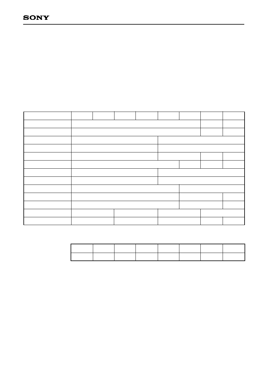
DCTRAN characteristics
Input amplitude [IRE]
20
40
60
80
100
B
l
a
c
k
s
i
n
k
l
e
v
e
l
[
m
V
]
≠250
≠200
≠150
≠100
≠50
0
Input: YIN 2Vp-p
Output: YOUT
SUBCONT = 7,
YDRIVE = A
SHARPNESS = 7
0
98.9%
Transmission rate
87.1%
78.4%
Transmission rate = (S ≠ black sink level) /S
S = 1.0Vp-p
DCTRAN = 0
DCTRAN = 3
DCTRAN = 7
TRAP attenuation
Frequency [MHz]
7
A
t
t
e
n
u
a
t
i
o
n
[
d
B
]
≠20
0
0
≠30
≠10
6
5
4
3
2
1
TRAPSW = 1
TRAPSW = 0
CTRAP ADJ = 9
Input: YIN
SWEEP
Output: YOUT
SUBCONT = 7
YDRIVE = F
DCTRAN = 0
SHARPNESS = 0
SHARPNESS = 7
SHARPNESS = F
SHARPNESS characteristics
Frequency [MHz]
1
2
3
4
5
6
7
8
G
a
i
n
[
d
B
]
≠6
≠4
≠2
0
2
4
6
8
0
SHPSW = 0
O
u
t
p
t
a
m
p
l
i
t
u
d
e
(
b
l
a
c
k
t
o
w
h
i
t
e
)
[
V
p
-
p
]
YDRIVE characteristics
Data
3
7
B
F
13
17
1B
1F
0.4
0.6
0.8
1.0
1.2
1.4
1.6
1.8
Input: YIN
1.4Vp-p (black to white)
Output: YOUT
SUBCONT = 7
DCTRAN = 0
SHARPNESS = 7
D
i
f
f
e
r
e
n
c
e
f
r
o
m
S
U
B
C
O
N
T
=
7
[
d
B
]
SUBCONT characteristics
Data
1
3
5
7
9
B
D
F
≠4
≠3
≠2
≠1
0
1
2
3
Input: YIN
1.4Vp-p (black to white)
Output: YOUT
YDRIVE = F
DCTRAN = 0
SHARPNESS = 7
Example of Representative Characteristics

≠ 28 ≠
CXA2019AQ
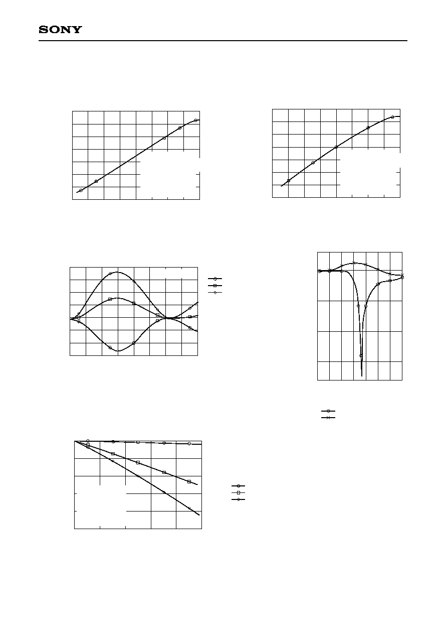
COLOR control characteristics
Data
7
F
17
1F
27
2F
37
3F
O
u
t
p
u
t
a
m
p
l
i
t
u
d
e
[
V
p
-
p
]
0
0.5
1.0
1.5
2.0
2.5
SUBCOLOR control characteristics
Data
1
3
5
7
9
B
D
F
D
i
f
f
e
r
e
n
c
e
f
r
o
m
S
U
B
C
O
L
O
R
=
7
[
d
B
]
≠6
≠4
≠2
0
2
4
Input: CVBS/YIN
75% COLORBAR 2Vp-p
Output: UOUT (YELLOW ≠ BLUE)
R2/V2DRIVE control characteristics
Data
3
7
B
F
13
17
1B
1F
O
u
t
p
u
t
a
m
p
l
i
t
u
d
e
[
V
p
-
p
]
0.4
0.8
1.0
1.2
1.4
1.6
Input: U2IN/V2IN
1Vp-p PULSE positive polarity
Output: U2OUT/V2OUT
0.6
U2DRIVE
V2DRIVE
UPED/VPED control characteristics
Data
1
3
5
7
9
B
D
F
D
i
f
f
e
r
e
n
c
e
f
r
o
m
v
i
d
e
o
b
l
a
c
l
e
v
e
l
f
o
r
o
u
t
p
u
t
[
m
V
]
≠10
0
10
Input: No signal
Output: UOUT/VOUT
SUBCOLOR = 7
COLOR = 1F
TOT characteristics
Difference from 3.579545MHz [MHz]
≠0.5
0
0.5
A
t
t
e
n
u
a
t
i
o
n
[
d
B
]
≠12
≠8
≠4
≠2
2
≠10
≠6
0
TOT = OFF
TOT = ON
≠1
AUTOPED characteristics
Input amplitude (black to white) [IRE]
20
40
60
80
100
O
u
t
p
u
t
a
m
p
l
i
t
u
d
e
(
b
l
a
c
k
t
o
w
h
i
t
e
)
[
I
R
E
]
0
20
40
60
80
100
0
Input: CVBS/YIN
75% COLORBAR 2Vp-p
Output: UOUT (YELLOW ≠ BLUE)
SUBCOLR = 7, SUBHUE = 7
HUE = 1F, TOT = 0
Input: YIN FLAT Signal
Outout: YOUT 100 IRE = 1.1Vp-p
DCTRAN = 0, TRAP = 0

≠ 29 ≠
CXA2019AQ
R2/V2PED control characteristics
Data
1
3
5
7
9
B
D
F
D
i
f
f
e
r
e
n
c
e
f
r
o
m
v
i
d
e
o
b
l
a
c
k
l
e
v
e
l
f
o
r
o
u
t
p
u
t
[
m
V
]
≠40
≠20
0
20
40
60
Input: No signal
Output: U2OUT/V2OUT
U2PED
V2PED
Y2DRIVE control characteristics
Data
3
7
B
F
13
17
1B
1F
O
u
t
p
u
t
a
m
p
l
i
t
u
d
e
(
b
l
a
c
k
t
o
w
h
i
t
e
)
[
V
p
-
p
]
0.4
0.5
0.6
0.7
0.8
0.9
1.0
1.1
ABL control characteristics
ABLFILIN voltage [V]
1
2
3
4
5
6
7
9
O
u
t
p
u
t
D
C
v
a
r
i
a
t
i
o
n
[
m
V
]
≠50
0
50
100
150
200
250
300
0
8
ABL = 1/ABLCENT = 3
ABL = 0/ABLCENT = 0
ABL = 0/ABLCENT = 3
Input: Y2IN
1Vp-p PULSE (positive polarity)
Output: Y2OUT
ABLOFF = 1
Input: Y2IN no signal
Output: Y2OUT
RYDRIVE = F

≠ 30 ≠
CXA2019AQ
Package Outline
Unit: mm
SONY CODE
EIAJ CODE
JEDEC CODE
PACKAGE MATERIAL
LEAD TREATMENT
LEAD MATERIAL
PACKAGE MASS
EPOXY RESIN
SOLDER / PALLADIUM
42/COPPER ALLOY
PACKAGE STRUCTURE
PLATING
0.2g
QFP-40P-L01
QFP040-P-0707
40PIN QFP (PLASTIC)
9.0 ± 0.4
+ 0.4
0.3 ≠ 0.1
1
10
11
20
21
30
31
40
1.5 ≠ 0.15
+ 0.35
0.127 ≠ 0.05
+ 0.1
(
8
.
0
)
A
A
DETAIL
0.1 ≠ 0.1
+ 0.15
+ 0.15
7.0 ≠ 0.1
0
.
5
±
0
.
2
0.1
M
± 0.12
0.65
NOTE : PALLADIUM PLATING
This product uses S-PdPPF (Sony Spec.-Palladium Pre-Plated Lead Frame).