 | –≠–ª–µ–∫—Ç—Ä–æ–Ω–Ω—ã–π –∫–æ–º–ø–æ–Ω–µ–Ω—Ç: CXA2096N | –°–∫–∞—á–∞—Ç—å:  PDF PDF  ZIP ZIP |
Digital CCD Camera Head Amplifier
Description
The CXA2096N is a bipolar IC developed as a
head amplifier for digital CCD cameras. This IC
provides the following functions: correlated double
sampling, AGC for the CCD signal, A/D sample and
hold, blanking, A/D reference voltage, and an output
driver.
Features
∑ High sensitivity made possible by a high-gain AGC
amplifier
∑ Blanking function provided for the purpose of
calibrating the CCD output signal black level
∑ Regulator output pin provided for A/D converter
reference voltage
∑ Built-in sample-and-hold circuits for camera signals
required by external A/D converters
Absolute Maximum Ratings
∑ Supply voltage
V
CC
11
V
∑ Operating temperature
Topr
≠20 to +75
∞C
∑ Storage temperature
Tstg
≠65 to +150
∞C
∑ Allowable power dissipation
P
D
417
mW
Operating Conditions
Supply voltage
V
CC
1, 2, 3 3.0 to 3.6
V
Applications
DVC/still cameras for consumer use
Structure
Bipolar silicon monolithic IC
≠ 1 ≠
E97449B8Y
Sony reserves the right to change products and specifications without prior notice. This information does not convey any license by
any implication or otherwise under any patents or other right. Application circuits shown, if any, are typical examples illustrating the
operation of the devices. Sony cannot assume responsibility for any problems arising out of the use of these circuits.
CXA2096N
24 pin SSOP (Plastic)
≠ 2 ≠
CXA2096N
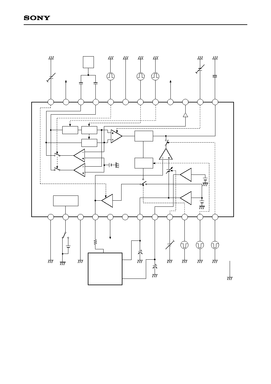
Block Diagram and Pin Configuration
BUF
V
RT
DMSW1
9
10
11
12
13
14
15
16
2
3
4
5
6
7
8
1
17
18
19
20
21
22
23
24
CDS
CLP1
AGC
SH3
DMSW2
CAM
SH
POWER
SAVE CONT
SH1
SH2
DC
SHIFT
V
RT
DRV
V
RB
DRV
V
RB
DRV
V
REF
CDS
CLP2
AGC
CLP
OB SW
OFFSET
BLK SW
I
C
O
N
T
V
C
C
2
D
I
N
P
I
N
C
L
P
D
M
G
N
D
1
S
H
D
S
H
P
V
C
C
1
C
C
D
L
E
V
E
L
A
G
C
C
O
N
T
A
G
C
C
L
P
G
N
D
2
P
S
G
N
D
3
D
R
V
O
U
T
V
C
C
3
N
.
C
.
V
R
B
V
R
T
O
F
F
S
E
T
P
B
L
K
X
R
S
C
L
P
O
B
≠ 3 ≠
CXA2096N
Pin Description
(V
CC
1, 2, 3 = 3V)
2
PS
Power saving mode.
1
3
19
GND2
GND3
GND1
Ground.
VTH = 1.5V
GND
145
5k
10µA
2
1.5V
60k
30k
4
DRVOUT
Driver output for A/D
converter capable of
DC coupling.
Dynamic range =
1Vp-p.
V
RB
to
V
RB
+ 100mV
5
16
23
V
CC
3
V
CC
1
V
CC
2
Power supply.
V
CC
CAM signal
48
50µA
145
I
CONT
3.2 to 6.4mA
200µA
50µA
25µA
25µA
2k
I
OFFSET
0 to
50µA
V
RB
=
1.35V
4
Pin
No.
Symbol
Pin voltage
Equivalent circuit
Description
≠ 4 ≠
CXA2096N
7
VRB
1.35V regulator
output.
Be sure to decouple
this pin near the IC
pins to prevent the
oscillation and external
noise when this pin is
not used.
(Recommended
capacitor value: 4.7µF)
1.35V
2.35V
8
VRT
2.35V regulator
output.
Be sure to decouple
this pin near the IC
pins to prevent the
oscillation and external
noise when this pin is
not used.
(Recommended
capacitor value: 4.7µF)
200
30k
16.5k
13.5k
145
1.35V
110µA
7
30k
6.5k
23.5k
145
2.35V
220µ
55µ
55µ
200
8
9
OFFSET
Controls the output
offset.
When 3V: V
RB
When 1.5V: V
RB
+
100mV
When 0V (preset
mode): V
RB
+ 35mV
1.5 to 3V
&
0V
2k
30k
30k
50k
50k
1.5k
3k
25k
V
RB
145
50µA
50µA
50µA
1.85V
9
10
PBLK
Camera signal
preblanking pulse
input.
Active when Low.
Calibrates the black
level of the AGC
output waveform.
When PBLK is Low,
the DRVOUT
potential is forced to
V
RB
.
VTH = 1.85V
145
50µA
30k
30k
1.85V
30k
10
Active: Low
6
N.C.
No connection;
normally ground.
Pin
No.
Symbol
Pin voltage
Equivalent circuit
Description
≠ 5 ≠
CXA2096N
11
XRS
Camera signal
sample-and-hold
pulse input.
VTH = 0.68V
24k
7k
0.68V
770µA
40µA
97µ
145
11
12
CLPOB
Clamp pulse used to
clamp the optical
black portion of the
camera signal after it
passes through the
AGC amplifier.
VTH = 1.5V
145
50µA
30k
30k
1.5V
30k
12
Sampling
Active: Low
13
AGCCLP
AGC clamp capacitor.
(Recommended
value: 0.1µF)
Approx. 1.3V
14
AGCCONT
AGC gain control.
When 1.5V: ≠1dB
(Minimum
gain)
When 3.0V: 31.5dB
(Maximum
gain)
1.5 to 3.0V
50k
145
145
5k
5k
3k
3k
13
145
200µA
3.4k
3.4k
200µA
2.14V
100µA
300µA
300µA
100µA
2.29V
I
CONT
3.4k
3.4k
3.3k
3.3k
14
Pin
No.
Symbol
Pin voltage
Equivalent circuit
Description
≠ 6 ≠
CXA2096N
Pin
No.
Symbol
Pin voltage
Equivalent circuit
Description
15
CCDLEVEL
Enables monitoring of
the SH3 output
camera signal.
CCD signal
black level of
DIN input
approx. 2.2V
17
SHP
Preset level sample-
and-hold pulse input.
18
SHD
Data level sample-
and-hold pulse input.
VTH = 0.65V
500
340
100µA
15
36k
10k
0.65V
365µA
20µA
145
17
18
Sampling
20
CLPDM
Clamp pulse used to
clamp the dummy
pixel portion of the
input CCD signal.
VTH = 1.5V
145
50µA
30k
30k
1.5V
20
21
22
24
PIN
DIN
ICONT
CCD signal input.
DRVOUT output
waveform rise time
control.
When 1.5V: Maximum
rise time
When 3V:
Minimum
rise time
Black level
approx. 2.1V
1.5 to 3V
145
145
200µA
50µA
23k
7k
14k
2k
2k
15µA
15µA
21
22
145
100µA
15k
45k
6k
6k
2.25V
24
Active: Low
≠ 7 ≠
CXA2096N
Electrical Characteristics
(Ta = 25∞C, V
CC
1, 2, 3 = 3V)
PS = OFF
(PS indicates
Power Save)
PS = ON
Maximum
gain
Minimum
gain
Range of gain
variance
Dynamic
range
maximum
Dynamic
range
typical
Offset high
Offset low
Offset
preset
V
RT
DC
level
V
RB
DC
level
V
RT
≠ V
RG
Offset
Dynamic
range
I
DC
I
DP
A CONT
max.
A CONT
min.
AGC G
AGCmax.
D
AGC
TYP
.
D
CAOF
high
CAOF
low
CAOF
pre
VRTO
VRBO
VR
BLKOF
SH3 D
AGCCONT = 1.5V, open between V
RT
and V
RB
PS = 3V, I
CONT
= 3V
PS = 0V
DIN = 1µs, 20mVp-p pulse
AGCCONT = 3V, I
CONT
= 3V
DIN = 1µs, 500mVp-p pulse
AGCCONT = 1.5V, I
CONT
= 3V
A CON max. ≠ A CON min.
AGCCONT = 3V
DRVOUT output signal at saturation level
AGCCONT = 2V
DRVOUT output signal at saturation level
OFFSET = 1.5V
OFFSET = 3.0V
OFFSET = 0V
With a 400
load
With a 400
load
With a 400
load
BLKOF (PBLK = 3V) ≠ BLKOF (PBLK = 0V)
DIN = 1µs, 1Vp-p pulse
Item
Symbol
Conditions
Min.
Typ.
Max. Unit
Current
consump
-tion
AGC
DRV
mA
dB
mV
mV
mV
mV
REF
BLK
25.1
0
28.5
--
27.1
800
900
80
--
25
2300
1300
950
≠15
600
37.1
1.8
31.3
≠0.8
32.1
970
960
98
2
34
2340
1353
988
9
790
49.0
4.2
--
1.4
--
--
--
--
5
40
2400
1400
1050
30
--
mV
SH3

≠ 8 ≠
CXA2096N
Electrical Characteristics Measurement Circuit
BUF
V
RT
DMSW1
9
10
11
12
13
14
15
16
2
3
4
5
6
7
8
1
17
18
19
20
21
22
23
24
CDS
CLP1
AGC
SH3
DMSW2
CAM
SH
POWER
SAVE CONT
SH1
SH2
DC
SHIFT
V
RT
DRV
V
RB
DRV
V
RB
DRV
V
REF
CDS
CLP2
AGC
CLP
OB SW
OFFSET
BLK SW
I
C
O
N
T
V
C
C
2
D
I
N
P
I
N
G
N
D
1
S
H
D
S
H
P
V
C
C
1
C
C
D
L
E
V
E
L
A
G
C
C
O
N
T
A
G
C
C
L
P
G
N
D
2
P
S
G
N
D
3
D
R
V
O
U
T
V
C
C
3
N
.
C
.
V
R
B
V
R
T
O
F
F
S
E
T
P
B
L
K
X
R
S
C
L
P
O
B
L
H
SW1
C3
0.1µF
V3
1.5 to 3V
V
CC
1
3V
PL3
PL2
PL1
C2
1µF
C1
1µF
AC
V2
V
CC
2
3V
V1
1.5 to 3V
GND
PL4
PL5
PL6
V4
0 to 3V
C4
4.7µ
C5
4.7µ
SW2
V
CC
3
3V
C6
40pF
R2
22
R3
10k
V5
1.85V
V6
3V
C
L
P
D
M
R1
400
SW1
H
L
POWER SAVE
OFF
ON

≠ 9 ≠
CXA2096N
Measurement Timing Chart
Different for each test
2.5V
GND
2.5V
GND
2.5V
GND
2.5V
GND
1H
2µs
2µs
1H
Equivalent to CCD signal black level
PL4 (CLPOB)
PL1 (CLPDM)
PL6 (PBLK)
V2 (DIN)
PL2 (SHD)
PL3 (SHP)
PL5 (XRS)
1H
≠ 10 ≠
CXA2096N
Application Circuit
V
AGCCONT
1.5 to 3V
BUF
V
RT
DMSW1
9
10
11
12
13
14
15
16
2
3
4
5
6
7
8
1
17
18
19
20
21
22
23
24
CDS
CLP1
SH3
DMSW2
CAM
SH
POWER
SAVE CONT
SH1
SH2
DC
SHIFT
V
RT
DRV
V
RB
DRV
V
RB
DRV
V
REF
CDS
CLP2
AGC
CLP
OB SW
OFFSET
BLK SW
I
C
O
N
T
V
C
C
2
D
I
N
P
I
N
G
N
D
1
S
H
D
S
H
P
V
C
C
1
C
C
D
L
E
V
E
L
A
G
C
C
O
N
T
A
G
C
C
L
P
G
N
D
2
P
S
G
N
D
3
D
R
V
O
U
T
V
C
C
3
N
.
C
.
V
R
B
V
R
T
O
F
F
S
E
T
P
B
L
K
X
R
S
C
L
P
O
B
0.1µF
SHP
SHD
CLPDM
1µF
1µF
V
ICONT
1.5 to 3V
CLPOB
XRS
PBLK
V
OFFSET
0 to 3V
4.7µF
4.7µ
22
V
CC
CCD
V
CC
3V
V
CC
V
RB
A/D IN
A/D
V
RT
GND
C
L
P
D
M
AGC
Application circuits shown are typical examples illustrating the operation of the devices. Sony cannot assume responsibility for
any problems arising out of the use of these circuits or for any infringement of third party patent and other right due to same.
≠ 11 ≠
CXA2096N
Description of Operation
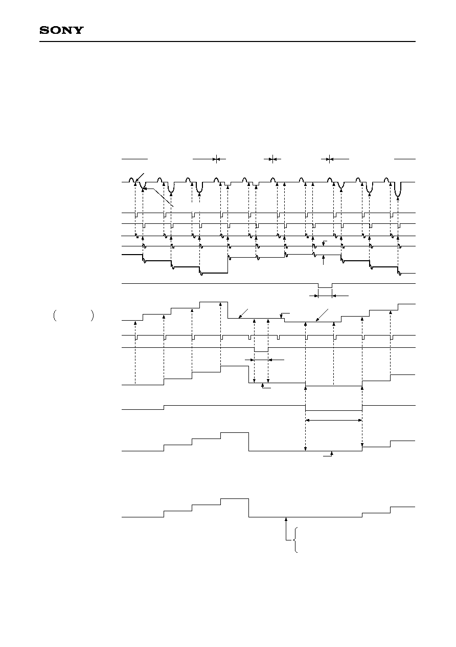
Refer to the Block Diagram.
Operating Conditions
The camera signal processing system operates when PS is High.
Timing Chart (when V
CC
= 3V)
PBLK
(10µ during the idle
transfer interval)
Signal interval
OPB interval
Signal interval
Precharge level
Signal level
2.1V
2.1V
[
1]
[
2]
2µs
0.65V
Black level
Basic black
level
[
3]
2µs
0.65V
10µs
1.35V
[
4]
[
5]
Approx. V
RB
+ 35mV when OFFSET = 0V
Approx. V
RB
+ 100mV when OFFSET = 1.5V
Applox. V
RB
when OFFSET = 3V
CCD output
SHP
SHD
SH1 output
SH2 output
SH3 output
CLPDM
(2µ dummy bit portion
during the idle transfer
interval)
XRS
CLPOB
(2µ during the OPB interval)
CAMSH output
BLK SW output
DRVOUT output
AGC output
SH3 output
≠SH2 output
◊
(≠N)
Idle transfer
interval

≠ 12 ≠
CXA2096N
CDS (SH1, SH2, SH3):
The CCD signal from the CCD image sensor is input to PIN and DIN where correlated double sampling (CDS)
is performed by SH1, SH2 and SH3. The precharge level of the CCD output signal is sampled, held and output
by the SH2 output, and the signal level is sampled, held and output by the SH3 output. SH1 and SH2 are the
sample-and-hold circuits for the precharge level; SH3 is the sample-and-hold circuit for the signal level.
CDSCLP 1, 2:
CDSCLP1 and 2 stabilize the input signal DC level, clamp (CLPDM) the input signal during the idle transfer
interval for the purpose of eliminating the AGC input offset, and adjust the DC level ([
1], [
2]) of SH2 and SH3
in line with V
REF
. CDSCLP1 is the clamp circuit for the precharge level, and CDSCLP2 is the clamp circuit for
the signal level.
AGC:
AGC is the gain control amplifier for the camera signal.
The gain can be varied from ≠1 to +31dB by adjusting the AGCCONT voltage control V
AGCCONT
from 1.5 to
3.0V.
CAM SH:
CAM SH is the sample-and-hold circuit for synchronizing the data read-in timing for the external A/D. Sampling
is possible according to the approximately 10ns sampling pulse width input to XRS.
AGCCLP:
The basic black level is set ([
3]) by clamping the AGC output waveform with the CLPOB clock during the OPB
interval. When PBLK is High and CLPOB is Low, the clamping circuit operates, adjusting the AGCCLP current
so that the DRVOUT potential equals the OFFSET potential (which is determined by the voltage applied to the
OFFSET pin), thus setting the AGCCLP potential. The AGCCLP capacitance is connected to the AGCCLP pin.
DC SHIFT:
This circuit functions when AGCCLP operates, following the AGCCLP potential and forcing a DC shift of the
AGC output waveform OPB interval to the basic black level. When AGCCLP is not operating, the basic black
level is maintained at its previous setting.
BLK SW:
The black level is calibrated by blanking the black level signal of the AGC output waveform so that it does not
fall below the basic black level and replacing the DC potential with V
RB
. ([
4])
The signal is blanked when PBLK is Low.
OFFSET:
OFFSET controls the DRV output waveform black level offset.
The offset of the DRVOUT camera signals can be adjusted when a voltage is applied to OFFSET. ([
5])
The voltage controlled by OFFSET is output as the DRV output DC offset via AGCCLP, DCSHIFT, CAMSH
and BLKSW.
When the OFFSET voltage is 1.5 to 3.0V, DRVOUT DC can vary in a linear fashion from V
RB
+ 100mV to V
RB
.
In addition, when the OFFSET voltage is 0V, DRVOUT DC is preset to V
RB
+ 35mV.

≠ 13 ≠
CXA2096N
DRV:
DRV drives the external A/D. The current that flows to the last-stage amplifier in DRV is controlled by applying
voltage to the ICONT pin, making it possible to adjust the rise time of the output waveform, which affects the
external A/D load capacitance. The variable range is 1.5 to 3V, with 1.5V yielding the maximum and 3V
yielding the minimum. The optimum rise time for the external A/D input capacitance can be selected.
V
RT
DRV, V
RB
DRV:
These are the external A/D reference voltage drivers. These circuits are connected to A/D V
RT
and V
RB
,
supplying 2.35V and 1.35V, respectively, when V
CC
is 3V. The IC's internal primary voltage is also generated
on the basis of the V
RT
and V
RB
voltage. (V
RB
, V
B
and V
CENT
)
POWER SAVE CONTROL:
The PS pin is the power save pin; the operating state is enabled when this pin is High, while the power saving
function operates when it is Low.
≠ 14 ≠
CXA2096N
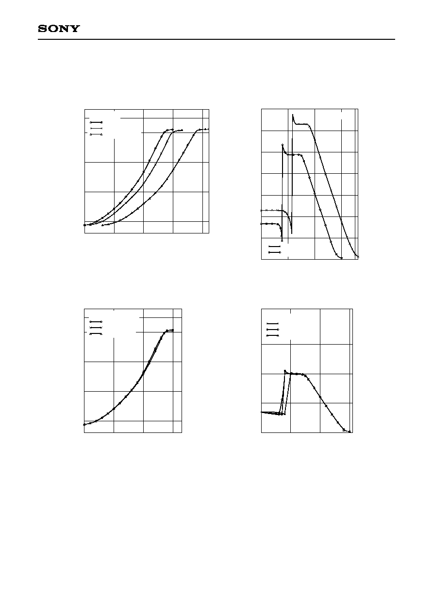
Characteristics Graphs
AGCCONT control supply voltage characteristics
V
AGCCONT
vs. Gain
V
AGCCONT
[V]
1.5
2.0
2.5
3.0
3.5
0
10
20
30
35
G
a
i
n
[
d
B
]
OFFSET control supply voltage characteristics
V
OFFSET
vs. OFFSET
V
OFFSET
[V]
0
1.0
2.0
3.0
3.5
20
40
60
80
100
O
F
F
S
E
T
[
m
V
]
≠4
(V
RB
=) 0
AGCCONT control temperature characteristics
AGCCONT vs. Gain
AGCCONT [V]
1.5
2.0
2.5
3.0
0
10
20
30
35
G
a
i
n
[
d
B
]
V
CC
= 3.0V
Tc = ≠20∞C
Tc = +27∞C
Tc = +75∞C
OFFSET control temperature characteristics
V
OFFSET
vs. OFFSET
V
OFFSET
[V]
0
1.0
2.0
3.0
50
100
O
F
F
S
E
T
[
m
V
]
V
CC
= 3.0V
150
Tc = ≠20∞C
Tc = +27∞C
Tc = +75∞C
(V
RB
=) 0
≠4
Tc = 27∞C
V
CC
= 3V
V
CC
= 3.15V
V
CC
= 3.6V
120
140
Tc = 27∞C
V
CC
= 3.6V
V
CC
= 3V

≠ 15 ≠
CXA2096N
Maximum signal amplitude temperature characteristics
(Min. gain)
Tc vs. Vout
Tc [∞C]
≠20
0.6
V
o
u
t
[
V
p
-
p
]
0.7
0.8
0
50
100
0.53
V
CC
= 3.0V, AGCCONT = 1.5V
Input amplitude DIN =
Input amplitude DIN =
Input amplitude DIN =
Input amplitude DIN =
Input amplitude DIN =
870mVp-p
800mVp-p
750mVp-p
700mVp-p
600mVp-p
0.9
DIN = 870mVp-p
DIN = 800mVp-p
DIN = 750mVp-p
DIN = 700mVp-p
DIN = 600mVp-p
Maximum signal amplitude temperature characteristics
(Max. gain)
Tc vs. Vout
Tc [∞C]
≠20
0.8
V
o
u
t
[
V
p
-
p
]
0.9
1.0
0
50
100
0.75
V
CC
= 3.0V, AGCCONT = 3.0V
Input amplitude DIN =
Input amplitude DIN =
Input amplitude DIN =
28mVp-p
24mVp-p
21mVp-p
30.99dB
30.99dB
30.76dB
31.41dB
31.41dB
31.03dB
31.45dB
31.45dB
31.12dB
DIN = 28mVp-p
30.99 dB
+0
≠0.23
DIN = 24mVp-p
31.41 dB
+0
≠0.38
DIN = 21mVp-p
31.45 dB
+0
≠0.33
Gain temperature characteristics
from ≠20 to +100∞C
V
RT
, V
RB
, V
RT
≠ V
RB
temperature characteristics
Tc vs. V
RT
, V
RB
, V
RT
≠ V
RB
V
CC
= 3.0V
Tc [∞C]
≠20
V
R
T
,
V
R
B
,
V
R
T
≠
V
R
B
[
V
]
0.8
80
0
20
40
60
2.4
2.2
2.0
1.8
1.6
1.4
1.2
1.0
V
RT
V
RB
V
RT
≠ V
RB
≠ 16 ≠
CXA2096N
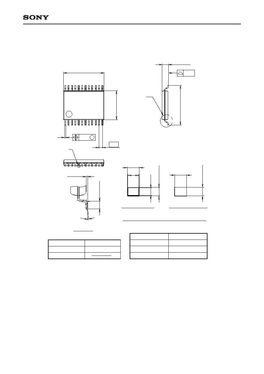
Package Outline
Unit: mm
SONY CODE
EIAJ CODE
JEDEC CODE
SSOP-24P-L01
SSOP024-P-0056
PACKAGE MATERIAL
LEAD TREATMENT
LEAD MATERIAL
PACKAGE MASS
EPOXY RESIN
SOLDER/PALLADIUM
42/COPPER ALLOY
PACKAGE STRUCTURE
PLATING
0.1g
24PIN SSOP(PLASTIC)
0.1 ± 0.1
0∞ to 10∞
0
.
5
±
0
.
2
DETAIL A
5
.
6
±
0
.
1
24
7.8 ± 0.1
13
0.65
12
1
7
.
6
±
0
.
2
0.1
1.25 ≠ 0.1
+ 0.2
A
0.13 M
NOTE: Dimension "
" does not include mold protrusion.
b=0.22 ≠ 0.05
+ 0.1
0
.
1
5
≠
0
.
0
2
+
0
.
0
5
(0.22)
(
0
.
1
5
)
0
.
1
5
≠
0
.
0
1
DETAIL B : SOLDER
DETAIL B : PALLADIUM
+
0
.
0
3
b=0.22 ± 0.03
B
b
NOTE : PALLADIUM PLATING
This product uses S-PdPPF (Sony Spec.-Palladium Pre-Plated Lead Frame).