 | –≠–ª–µ–∫—Ç—Ä–æ–Ω–Ω—ã–π –∫–æ–º–ø–æ–Ω–µ–Ω—Ç: CXA2153 | –°–∫–∞—á–∞—Ç—å:  PDF PDF  ZIP ZIP |
CXA2153S
Preamplifier for High Resolution Computer Display
Description
The CXA2153S is a bipolar IC developed for high
resolution computer displays.
Features
∑ Built-in wide-band amplifier: 180MHz@≠3dB (Typ.)
∑ Input dynamic range: 1.0Vp-p (Typ.)
∑ High gain preamplifier (15dB)
∑ R, G and B incorporated in a single package
(SDIP 30 pins)
∑ I
2
C bus control
Contrast control
R/G/B drive control
Brightness control
OSD contrast control
4-channel DAC control output
∑ Built-in gamma function
∑ Built-in high-speed ABL blanking
∑ Built-in sync separator for Sync on Green
∑ Built-in blanking mixing function
(with blanking level fixed at 0.4V)
∑ Built-in OSD mixing function
∑ Video period detection function
∑ Built-in VBLK synchronous DAC refresh system
Applications
High resolution computer displays
Structure
Bipolar silicon monolithic IC
Absolute Maximum Ratings (Ta = 25∞C, GND = 0V)
∑ Supply voltage
Vcc12
13
V
Vcc5
5.5
V
∑ Operating temperature Topr
≠20 to +75
∞C
∑ Storage temperature
Tstg
≠65 to +150
∞C
∑ Allowable power dissipation
P
D
2.05
W
∑ Pin voltage
Vcc5 + 0.3V
1, 3, 4, 6, 7, 8, 9, 10, 11,
12, 13, 14, 15, 16, 17 (Pin)
VREF (Pin 23) + 0.3V
18, 19, 20, 21, 25, 27,
29 (Pin)
Recommended Operating Conditions
Supply voltage
Vcc12
12 ± 0.5
V
Vcc5
5 ± 0.25
V
≠ 1 ≠
E99X02A1Y-PS
Sony reserves the right to change products and specifications without prior notice. This information does not convey any license by
any implication or otherwise under any patents or other right. Application circuits shown, if any, are typical examples illustrating the
operation of the devices. Sony cannot assume responsibility for any problems arising out of the use of these circuits.
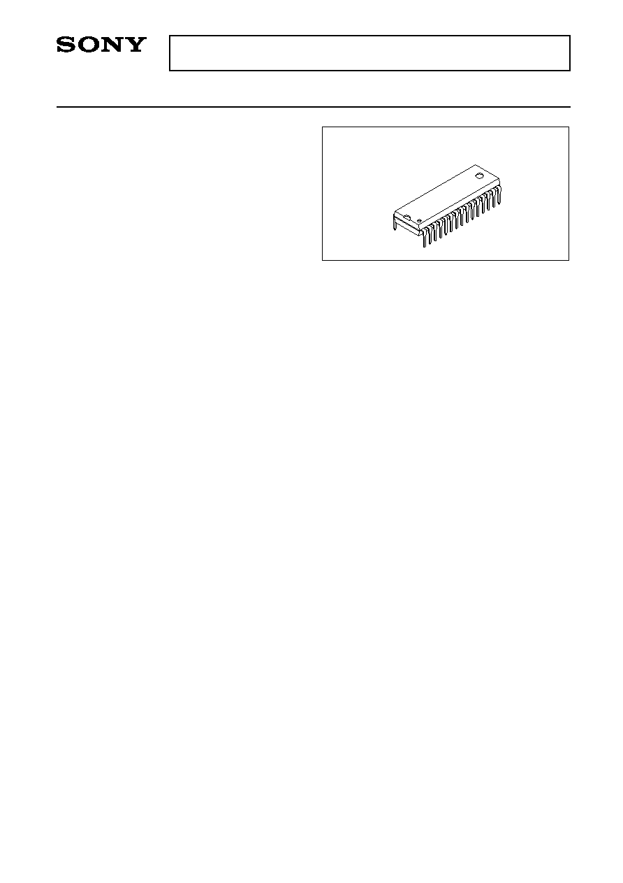
30 pin SDIP (Plastic)
≠ 2 ≠
CXA2153S
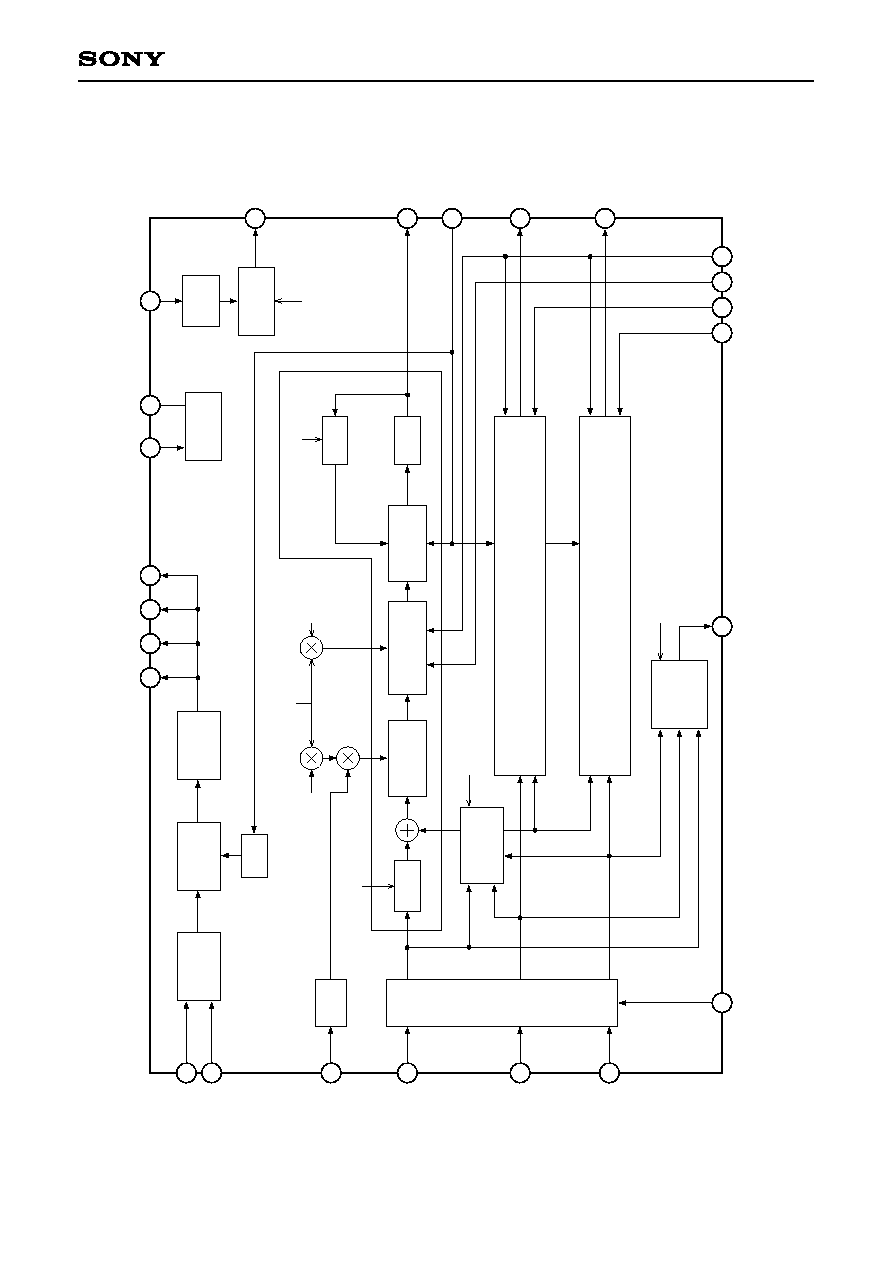
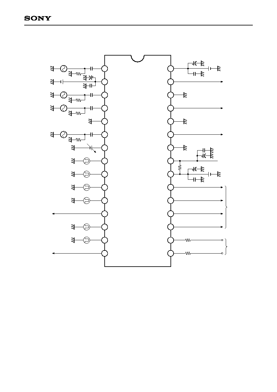
Block Diagram
I
2
C Bus
Decoder
Clamp
BIN
GIN
RIN
ABL
SCL
SDA
Rch
Gch
Bch
Latch
LPF
D/A
Converter
Regulator
BRIGHTNESS
Rch
AMP
Blanking Mix
OSD/OSD_BLK
Mix
DRIVE
OSD GAIN
G2
B_BKG
G_BKG
R_BKG
V
CC
12
VREF
SYNCIN
SHP
GAIN/
SHP
WIDTH
Contrast
V
ideo
Detector
Gain Control
AMP
Gch (Same as Rch)
BLK
Bch (Same as Rch)
VDET
LEVEL/VDET
OFF
Sharpness
Clamp
Clamp
ROUT
BLK
GOUT
BOUT
OSD_BLK
OSD_R
OSD_G
OSD_B
VDET
CLP
SYNCOUT
Buf
fer
Gamma
SYNC SEP
.
SYNC OFF
ABL
GAMMA1/GAMMA2/GM OFF
POL1/POL2
18
19
20
21
22
23
4
12
29
14
27
25
8
9
10
11
15
13
6
3
1
7
17
16
≠ 3 ≠
CXA2153S
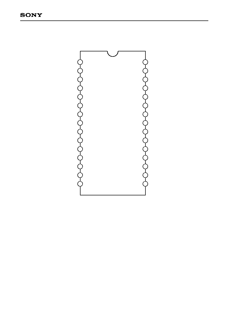
Pin Configuration
30
29
28
27
26
25
24
23
22
21
20
19
18
17
16
1
2
3
4
5
6
7
8
9
10
11
12
13
14
15
V
CC
12
ROUT
GND_R
GOUT
GND_G
BOUT
GND_B
VREF
V
CC
12
R_BKG
G_BKG
B_BKG
G2
SCL
SDA
RIN
V
CC
5
GIN
SYNCIN
GND
BIN
ABL
OSD_BLK
OSD_R
OSD_G
OSD_B
SYNCOUT
CLP
BLK
VDET
≠ 4 ≠
CXA2153S
Pin Description
Pin
No.
Symbol
Pin voltage
Equivalent circuit
Description
1
3
6
RIN
GIN
BIN
3.1V
(CLAMP)
RGB signal inputs.
Input via the capacitor.
7
ABL
2.5V
(when
open)
ABL input.
8
OSD_BLK
OSD_BLK control input.
VILMAX = 0.8V
VIHMIN = 2.8V
4
SYNCIN
2.9V
Sync-on-green signal input.
Input via the capacitor.
2
Vcc5
5V
5V power supply.
5
GND
GND
1
6
3
V
CC
V
CC
V
CC
1k
1k
1k
4
V
CC
V
CC
V
CC
100
150
V
CC
5V
20k
10k
10k
500
500
2k
V
CC
V
CC
V
CC
7
8
V
CC
30k
5k
V
CC
5k
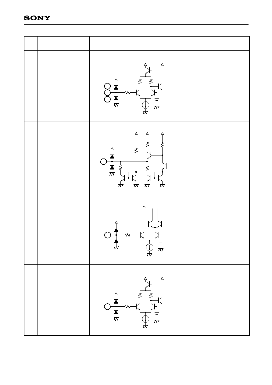
≠ 5 ≠
CXA2153S
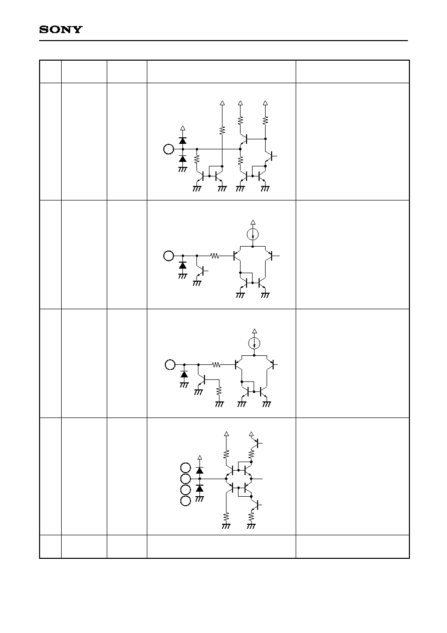
9
10
11
OSD_R
OSD_G
OSD_B
OSD control input.
VILMAX = 0.8V
VIHMIN = 2.8V
12
SYNCOUT
Sync separator output of Sync-
on-green signal.
I
2
C bus SOG off: Output at 0.
Typ.: High = 4.2V
Low = 0.2V
(positive polarity)
13
CLP
Clamp pulse (positive polarity)
input.
VILMAX = 0.8V
VIHMIN = 2.8V
14
BLK
Blanking pulse input.
Set the V blanking pulse width
to 300µs or more.
VILMAX = 1.2V
VIHMIN = 4.7V
10
9
11
V
CC
30k
V
CC
V
CC
5k
5k
12
V
CC
V
CC
V
CC
100
200
20k
5k
V
CC
200
13
V
CC
30k
V
CC
14
V
CC
30k
V
CC
V
CC
5k
5k
Pin
No.
Symbol
Pin voltage
Equivalent circuit
Description
≠ 6 ≠
CXA2153S
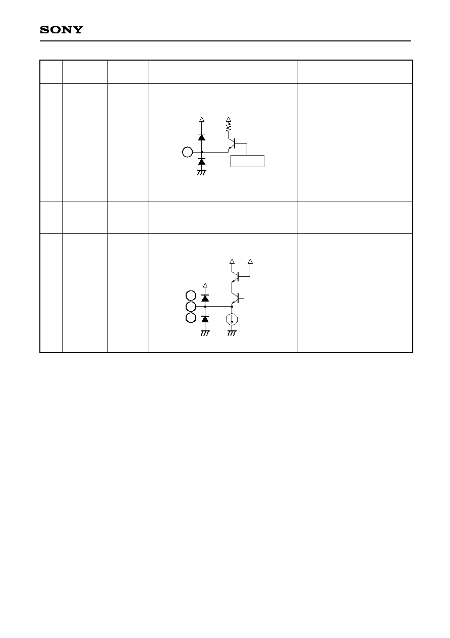
15
VDET
Video detector output.
I
2
C bus VDET off: Output at 0.
16
SDA
I
2
C bus standard SDA (serial
data) input/output.
VILMAX = 1.5V
VIHMIN = 3.5V
VOLMAX = 0.4V
15
V
CC
V
CC
VREF
100
200
20k
10k
V
CC
200
16
4k
V
CC
17
SCL
I
2
C bus standard SCL (serial
clock) input.
VILMAX = 1.5V
VIHMIN = 3.5V
17
4k
10k
V
CC
21
20
19
18
R_BKG
G_BKG
B_BKG
G2
BKG/G2 adjustment DAC
outputs.
The output DC is 1.5 to 5.5V.
22
30
Vcc12
12V
12V power supply
20
21
19
18
V
CC
VREG
VREG
1k
100
1k
100
Pin
No.
Symbol
Pin voltage
Equivalent circuit
Description
≠ 7 ≠
CXA2153S
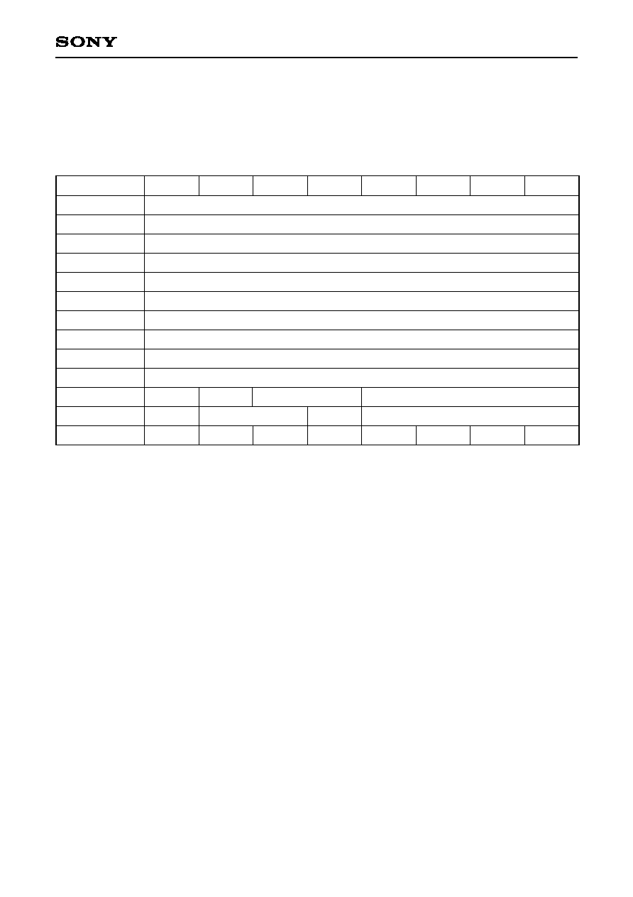
23
VREF
9V
9V regulator.
Connect with Vcc12 via a
resistor of around 220
.
It cannot be used as an
external power supply.
28
26
24
GND_R
GND_G
GND_B
0V
GNDs
29
27
25
ROUT
GOUT
BOUT
R, G and B signal outputs.
V
CC
12
Band Gap
V
CC
12
23
27
29
25
V
CC
V
CC
12 VREG
Pin
No.
Symbol
Pin voltage
Equivalent circuit
Description
≠ 8 ≠
CXA2153S
I
2
C BUS Register Definitions
Slave Address
SLAVE RECEIVER: 40 (HEX)
Register Table
00h
01h
02h
03h
04h
05h
06h
07h
08h
09h
0Ah
0Bh
0Ch
CONTRAST
BRIGHTNESS
R_BKG
G_BKG
B_BKG
OSD GAIN
G2
R_DRV
G_DRV
B_DRV
Sub Address
BIT 7
BIT 6
BIT 5
BIT 4
BIT 3
BIT 2
BIT 1
BIT 0
SHP WIDTH
SHP GAIN
POL1
GAMMA1
POL2
GAMMA2
VDET LVL VDET OFF SOG OFF GAM OFF
0
D R OFF
: Don't Care
Sub Address 0000 CONTRAST (8)
Controls the gain common to the R, G and B channels. Since control is
performed by multiplying with R/G/B DRIVE, the white balance can be
adjusted by R/G/B DRIVE and the luminance can be adjusted by
CONTRAST.
0: Output level minimum (0Vp-p)
255: Output level maximum (4.4Vp-p; with 0.7Vp-p input)
Sub Address 0001 BRIGHTNESS (8) Controls the black level common to the R, G and B channels.
0: Black level minimum (0.8V)
255: Black level maximum (2.9V)
Sub Address 0010 R_BKG (8)
Controls Pin 21 (R BACKGROUND) output voltage.
0: Output voltage minimum (1.5V)
255: Output voltage maximum (5.5V)
Sub Address 0011 G_BKG (8)
Controls Pin 20 (G BACKGROUND) output voltage.
0: Output voltage minimum (1.5V)
255: Output voltage maximum (5.5V)
Sub Address 0100 B_BKG (8)
Controls Pin 19 (B BACKGROUND) output voltage.
0: Output voltage minimum (1.5V)
255: Output voltage maximum (5.5V)

≠ 9 ≠
CXA2153S
Sub Address 0101 OSD GAIN (8)
Controls the OSD gain common to the R, G and B channels. Since
control is performed by multiplying with R/G/B DRIVE, the video white
balance and tracking are obtained.
0: Gain minimum (0Vp-p)
255: Gain maximum (4.5Vp-p)
Sub Address 0110 G2 (8)
Controls Pin 18 (G2) output voltage.
0: Output voltage minimum (1.5V)
255: Output voltage maximum (5.5V)
Sub Address 0111 R_DRV (8)
Controls the gain for the R channel. Control is performed by multiplying
with CONTRAST. Use this for adjusting the white balance.
0: Output level minimum (0Vp-p)
255: Output level maximum (4.4Vp-p; with 0.7Vp-p input)
Sub Address 1000 G_DRV (8)
Controls the gain for the G channel. Control is performed by multiplying
with CONTRAST. Use this for adjusting the white balance.
0: Output level minimum (0Vp-p)
255: Output level maximum (4.4Vp-p; with 0.7Vp-p input)
Sub Address 1001 B_DRV (8)
Controls the gain for the B channel. Control is performed by multiplying
with CONTRAST. Use this for adjusting the white balance.
0: Output level minimum (0Vp-p)
255: Output level maximum (4.4Vp-p; with 0.7Vp-p input)
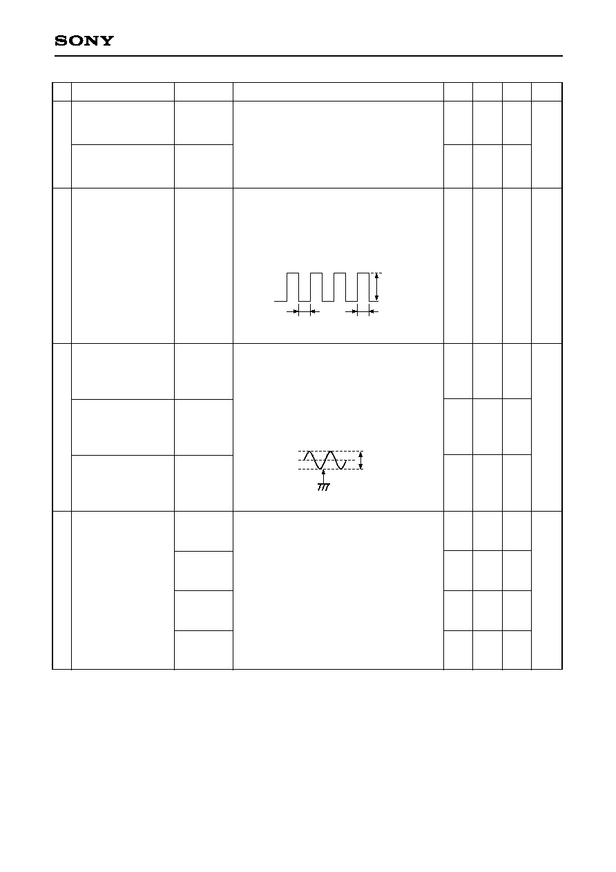
Sub Address 1010 SHP WIDTH (2)
Controls the sharpness time constant switching.
0: OFF
1: 25ns
2: 50ns
3: 100ns
Sub Address 1010 SHP GAIN (4)
Controls the sharpness gain.
0: Gain minimum (0dB)
F: Gain maximum (6dB)
Amplitude at SHP OFF is assumed to be 0dB.
Sub Address 1011 POL1 (1)
Controls the polarity of the correction at GAMMA1.
0: ≠ correction
1: + correction
Sub Address 1011 GAMMA1 (2)
Controls the gain of the inflection point 1 (15 IRE) at GAMMA.
0: 0 IRE correction
3: 9 IRE correction
Sub Address 1011 POL2 (1)
Controls the polarity of the correction at GAMMA2.
0: ≠ correction
1: + correction

≠ 10 ≠
CXA2153S
Sub Address 1011 GAMMA2 (4)
Controls the gain of the inflection point 2 (60 IRE) at GAMMA.
0: 0 IRE correction
7: 20 IRE correction
Sub Address 1100 VDET LVL (1)
Controls the signal detection (VDET) slice level.
0: Slice level (160mV when RIN or GIN or BIN)
1: Slice level (200mV when RIN or GIN or BIN)
Sub Address 1100 VDET OFF (1)
Controls the video detection output.
0: Output on
1: Output off
Sub Address 1100 SOG OFF (1)
Controls the sync separator output.
0: Output on
1: Output off
Sub Address 1100 GM OFF (1)
Controls the gamma function operation.
0: Gamma on
1: Gamma off
Sub Address 1100 D R OFF (1)
Controls the VBLK synchronous DAC refresh function. The operation of
this function is set to OFF when the power is turned on.
0: Function operation on
1: Function operation off
≠ 11 ≠
CXA2153S
I
2
C BUS Logic System
High level input voltage
Low level input voltage
Low level output voltage
SDA during current inflow of 3mA
Maximum clock frequency
Minimum waiting time for data change
Minimum waiting time for data transfer start
Low level clock pulse width
High level clock pulse width
Minimum waiting time for start preparation
Minimum data hold time
Maximum data preparation time
Rise time
Fall time
Minimum waiting time for stop preparation
1
2
3
4
5
6
7
8
9
10
11
12
13
14
V
IH
V
IL
V
OL
f
SCL
t
BUF
t
HD
; STA
t
LOW
t
HIGH
t
SU
; STA
t
HD
; DAT
t
SU
; DAT
t
R
t
F
t
SU
; STO
3.0
0
0
0
1.3
0.6
1.3
0.6
0.6
0
100
--
--
0.6
--
--
--
--
--
--
--
--
--
--
--
--
--
--
5.0
1.5
0.4
400
--
--
--
--
--
900
--
1
300
--
V
V
V
kHz
µs
µs
µs
µs
µs
ns
ns
µs
ns
µs
No.
Item
Symbol
Min.
Typ.
Max.
Unit
≠ 12 ≠
CXA2153S
Electrical Characteristics
No.
Measurement item
Symbol
Measurement contents
Min.
Typ. Max. Unit
1
2
3
4
5
6
7
Current
consumption (5V)
Current consumption
(12V)
Current consumption
(12V OFF)
Pulse characteristics
Contrast control 1
Contrast control 2
Relative contrast
Icc1
Icc2
Icc3
TR
TF
GCONT1
GCONT2
GCONGAP
Vcc5 (5V) pin inflow current
RGB signal input: None
Vcc12 (12V) pin inflow current
RGB signal input: None
Pin inflow current when 12V OFF
RGB signal input: None
Measure input rise time (TR1), input fall time
(TF1), input rise time (TR2) and input fall
time (TF2), then substitute these values into
the following equations.
TR =
(TR2
2
≠ TR1
2
), TF =
(TF2
2
≠ TF1
2
)
(Contrast = 7F, DRIVE = FF, BRIGHTNESS = 7F)
Measure the level of the output signal
amplitude Vout when a 0.7Vp-p video signal
is input.
GCONT1: Contrast = DRIVE = FF
GCONT2: Contrast = 00/DRIVE = FF
Calculate the difference in the data obtained
in No.5 and No.6 between the channels.
38
28
3.4
0.9
1.6
4
≠100
≠180
55
42
4.9
1.96
3.1
4.4
0
0
73
57
6.6
3
4.6
4.8
120
180
mA
mA
mA
ns
Vp-p
mVp-p
mV
TR
VIDEO amplitude 90%
VIDEO amplitude 0%
TF
0.7Vp-p
Input signal
≠ 13 ≠
CXA2153S
8
9
10
11
12
13
Drive control
OSD gain control
Relative OSD
Brightness control
Relative brightness
BLK level
GDRV
GOSD1
GOSD2
OSDGAP
VBRT1
VBRT2
VBRTGAP
VBLK
Measure the level of the output signal
amplitude Vout when a 0.7Vp-p video
signal is input.
Contrast = FF/DRIVE = 00
Measure the OSD level of the output signal
when the OSD pulse is input.
GOSD1: OSD = FF/DRIVE = FF
GOSD2: OSD = 00/DRIVE = FF
Calculate the difference in the data obtained
in No.9 between the channels.
Measure the black level of the RGB output
signal.
VBRT1: Brightness = 00
VBRT2: Brightness = FF
Calculate the difference in the data obtained
in No.11 between the channels.
Measure the BLK level of the output signal
when a BLK pulse is input.
≠100
4
≠330
≠200
0.6
2.5
≠200
0.13
0
4.57
0
0
0.8
2.93
0
0.43
120
5.15
360
200
0.95
3.28
200
0.74
mVp-p
Vp-p
mVp-p
mV
V
mV
V
0.7Vp-p
Input signal
OSD
level
OSD period
RGB output signal
No.
Measurement item
Symbol
Measurement contents
Min.
Typ. Max. Unit
GND
RGB output signal
Black level
GND
BLK level
≠ 14 ≠
CXA2153S
14
15
16
17
18
Sync separator
output rise delay
Sync separator
output fall delay
Sync separator
output
Sync separator
capacity
VDET output rise
delay
VDET output fall
delay
VDET output
SDLYR
SDLYF
Sync-Hi
Sync-Lo
SyncChk
DDLYR
DDLYF
VDET-Hi
VDET-Lo
Gradually reduce the sync level when the
duty is cycle 4.8% and 22.7% from 0.3Vp-p
and measure the sync level at which the
sync signals can be separated.
6.5
6.5
3.9
--
0.24
5.5
8.5
4
--
8.5
8.8
4
0.2
--
7.2
11.9
4.1
0.25
11
11
--
0.45
--
10
15.5
--
0.4
ns
V
Vp-p
ns
V
Vth = 50%
Vth = 50%
Rise Delay
Fall
Delay
Sync-IN
Sync-OUT
GND
Sync-Hi
Sync-Lo
Sync separator output
Vth = 50%
Vth = 50%
Fall
Delay
Rise
Delay
0.7Vp-p
RGB input
VDET output
GND
VDET-Hi
VDET-Lo
VDET output
No.
Measurement item
Symbol
Measurement contents
Min.
Typ. Max. Unit
≠ 15 ≠
CXA2153S
19
20
21
DAC output voltage
(BKG = 00)
DAC output voltage
(BKG = FF)
VDET output
amplitude
Sharpness gain 1
Sharpness gain 2
Sharpness gain 3
VBKG1
VBKG2
VDET
SHP1
SHP2
SHP3
Measure the DAC output voltage (Pin 20)
when BKG = 00/FF.
Input the crosshatch signal of Dot Clock
100MHz/ 0.7p-p to the RGB inputs, and
measure the VDET output amplitude.
VDET LEVEL = 0
Input a 10MHz sin wave to RGB at an
amplitude of 0.1Vp-p, and measure the
output level.
(CONTRAST: 7F/DRIVE: FF/ABL: 5V)
SHP1: SHP GAIN = F/SHP SW = 0
SHP2: SHP GAIN = 0/SHP SW = 3
SHP3: SHP GAIN = F/SHP SW = 3
Input 15 [IRE] and 60 [IRE] amplitude
signals (100 [IRE] = 0.7Vp-p) to the RGB
inputs, and measure the output amplitude.
GAM1: GAMMA1 = 3/POL1 = 1,
Vin = 0.105Vp-p
GAM2: GAMMA1 = 3/POL1 = 0,
Vin = 0.105Vp-p
GAM3: GAMMA2 = F/POL2 = 1,
Vin = 0.42Vp-p
GAM4: GAMMA2 = F/POL2 = 0,
Vin = 0.42Vp-p
(CONTRAST: 7F/DRIVE: FF/ABL: 5V)
1.25
5.45
3.35
0.3
0.3
0.6
1.45
5.7
3.8
0.4
0.4
0.8
1.67
5.95
4.4
0.5
0.5
1.0
V
Vp-p
Vp-p
Vp-p
Input signal
0.7Vp-p
10ns
10ns
0.1Vp-p
CLP potential
(approximately 3.1V)
Input signal
No.
Measurement item
Symbol
Measurement contents
Min.
Typ. Max. Unit
22 Gamma correction
GAM1
GAM2
GAM3
GAM4
0.65
0.15
2.1
1.0
0.5
0.05
1.8
0.8
0.8
0.25
2.4
1.25
≠ 16 ≠
CXA2153S
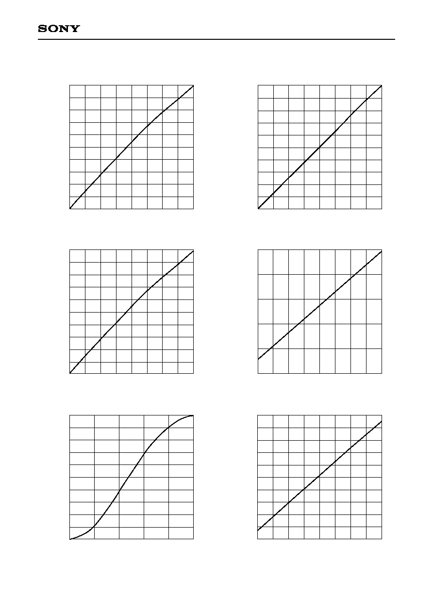
Control Characteristics
DRIVE Control Characteristics
DRIVE data
Output level [Vp-p]
RGB BKG/G2 Control Characteristics
Control data
Output voltage [V]
ABL Control Characteristics
ABL pin voltage [V]
RGB output amplitude [%]
CONTRAST Control Characteristics
CONTRAST data
Output level [Vp-p]
OSD GAIN Control Characteristics
OSD GAIN data
Output level [Vp-p]
BRIGHTNESS Control Characteristics
BRIGHTNESS data
Output voltage [V]
96
128
160
192
224
0
0
0.5
1.0
1.5
2.0
2.5
3.0
3.5
4.0
4.5
5.0
32
64
256
96
128
160
0
1.0
1.5
2.0
2.5
3.0
3.5
4.0
4.5
5.0
5.5
6.0
32
64
256
224
192
3
4
0
1
2
0
20
10
30
50
40
70
60
80
90
100
5
96
160
128
224
192
0
0
1.5
1.0
0.5
2.0
2.5
3.0
4.0
3.5
4.5
5.0
32
64
256
96
64
32
224
192
128
160
0
256
0
1.5
1.0
0.5
2.0
2.5
3.0
3.5
4.0
4.5
5.0
0.5
1.5
1.0
2.0
2.5
3.0
96
64
32
224
192
128
160
0
256
≠ 17 ≠
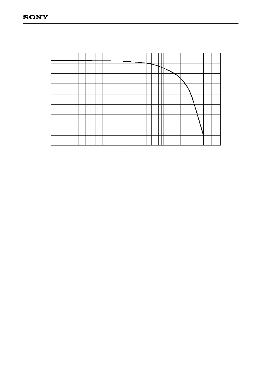
CXA2153S
14
12
10
8
6
4
2
0
≠2
≠4
1
10
100
1000
Input frequency [MHz]
Output gain [dB]
Frequency Characteristic
≠ 18 ≠
CXA2153S
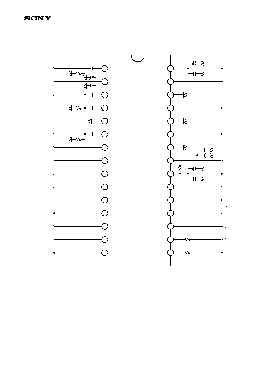
Electrical Characteristics Measurement Circuit
V
CC
12
ROUT
GND_R
GOUT
GND_G
BOUT
GND_B
VREF
V
CC
12
R_BKG
G_BKG
B_BKG
G2
SCL
SDA
RIN
V
CC
5
GIN
SYNCIN
GND
BIN
ABL
OSD_BLK
OSD_R
OSD_G
OSD_B
SYNCOUT
CLP
BLK
VDET
12V
0.1
µ
F
47
µ
F
0.1
µ
F
10
µ
F
12V
0.1
µ
F
47
µ
F
0.1
µ
F
75
220
Rch Output
Gch Output
Bch Output
220
I
2
C Bus
DAC
Output
SYNC SEP Output
VDET Output
220
0.1
µ
F
75
0.1
µ
F
0.1
µ
F
47
µ
F
75
0.1
µ
F
75
5V
1
2
3
4
5
6
7
8
9
10
11
12
13
14
15
30
29
28
27
25
24
23
22
21
20
19
18
17
16
26

≠ 19 ≠
CXA2153S
Electrical Characteristics Measurement Circuit (Frequency Response)
V
CC
12
ROUT
GND_R
GOUT
GND_G
BOUT
GND_B
VREF
V
CC
12
R_BKG
G_BKG
B_BKG
G2
SCL
SDA
RIN
V
CC
5
GIN
SYNCIN
GND
BIN
ABL
OSD_BLK
OSD_R
OSD_G
OSD_B
SYNCOUT
CLP
BLK
VDET
12V
0.1
µ
F
47
µ
F
0.1
µ
F
10
µ
F
12V
0.1
µ
F
47
µ
F
0.1
µ
F
75
220
Rch Output
Gch Output
Bch Output
VREF
220
I
2
C Bus
DAC
Output
SYNC SEP Output
VDET Output
220
0.1
µ
F
1k
0.1
µ
F
0.1
µ
F
47
µ
F
75
0.1
µ
F
75
5V
1
2
3
4
5
6
7
8
9
10
11
12
13
14
15
30
29
28
27
25
24
23
22
21
20
19
18
17
16
26
1k
1k
5V
≠ 20 ≠
CXA2153S
Application Circuit
V
CC
12
ROUT
GND_R
GOUT
GND_G
BOUT
GND_B
VREF
V
CC
12
R_BKG
G_BKG
B_BKG
G2
SCL
SDA
RIN
V
CC
5
GIN
SYNCIN
GND
BIN
ABL
OSD_BLK
OSD_R
OSD_G
OSD_B
SYNCOUT
CLP
BLK
VDET
0.1
µ
F
47
µ
F
0.1
µ
F
10
µ
F
0.1
µ
F
47
µ
F
0.1
µ
F
75
220
Rch Output
Gch Output
Bch Output
12V
12V
220
I
2
C Bus
DAC
Output
SYNC SEP Output
Bch Input
Gch Input
Rch Input
VDET Output
220
0.1
µ
F
75
0.1
µ
F
0.1
µ
F
47
µ
F
0.1
µ
F
75
1
2
3
4
5
6
7
8
9
10
11
12
13
14
15
30
29
28
27
25
24
23
22
21
20
19
18
17
16
26
Application circuits shown are typical examples illustrating the operation of the devices. Sony cannot assume responsibility for
any problems arising out of the use of these circuits or for any infringement of third party patent and other right due to same.
≠ 21 ≠
CXA2153S
Description of Operation
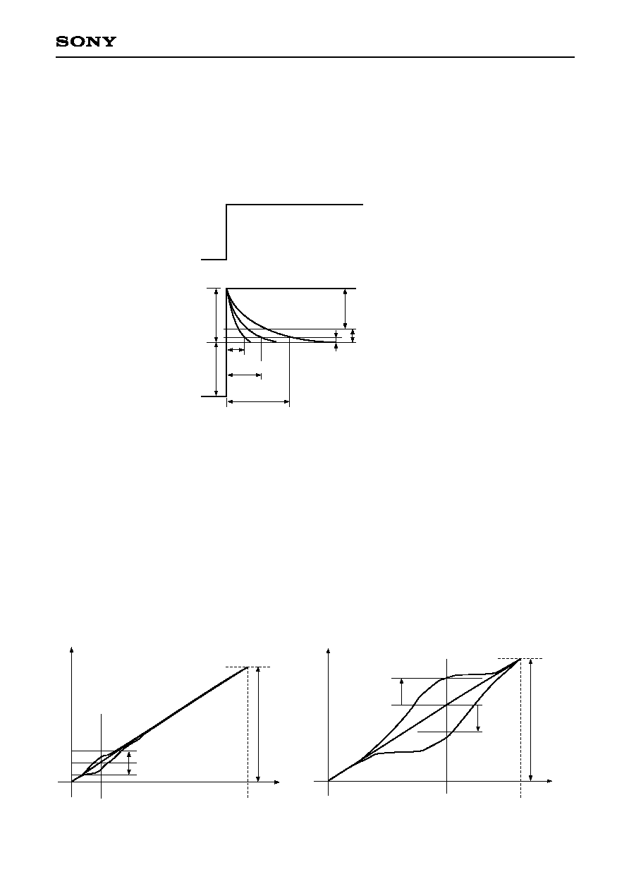
1. Sharpness function
The RGB signals input to Pins 5, 7 and 10 are mixed at a ratio of 0.6G + 0.3R + 0.1B to form the Y signal. The
high-frequency component is removed from this Y signal by a differentiation circuit, and the amplitude is
controlled by a gain control circuit. The signal which undergoes gain control (sharpness component) has its
amplitude clipped by a limiter circuit and is then added to the R, G and B signals.
Limiter level = 30% (Typ.)
Section not sent to RGB output because of the limiter
The output level when RIN = GIN = BIN = 0.7Vp-p
is set to 100%.
No sharpness component
10%
50ns
(T SW = 2)
100ns
(T SW = 3)
100%
100%
SHP GAIN = F (HEX)
SHP GAIN = 0 (HEX)
or SHP OFF = 1
25ns
(T SW = 1)
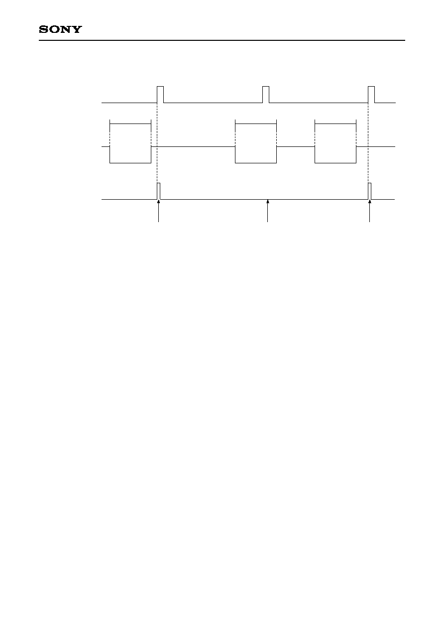
2. VBLK synchronous DAC refresh system
The VBLK signal is removed from the composite BLK signal which has been input to Pin 14, and the data for
each control DAC is overwritten all at once in synchronization with this VBLK signal. The received I
2
C bus data
is held by a latch until the next VBLK signal arrives. As a result, I
2
C bus data transmission from the
microcomputer is timing-free. Set the width of the V blanking pulse which is input to Pin 14 to 300µs or more.
(See the next page)
3. Gamma correction function
Using the output obtained when 700mVp-p RGB signals are input as a reference (100 [IRE]), the ±9 [IRE]
(GAMMA1) and ±20 [IRE] (GAMMA2) waveforms can be corrected at the 15 [IRE] and 60 [IRE] inflection points,
respectively.
The polarity switching gain can be controlled separately for each point, enabling correction broken at two
points. The I
2
C bus controls the polarity switching and gain correction.
+9 [IRE]
≠9 [IRE]
15 [IRE]
100 [IRE]
100 [IRE]
GAMMA1
0
≠20 [IRE]
+20 [IRE]
0
100 [IRE]
60 [IRE]
100 [IRE]
GAMMA2
≠ 22 ≠
CXA2153S
VBLK Synchronous DAC Refresh System
The VBLK signal is extracted from the composite BLK signal which has been input to Pin 14, and the DAC data
for each control is rewritten all at once in synchronization with this VBLK signal. The received I
2
C bus data is held
by a latch until the next VBLK signal arrives. Therefore, I
2
C bus data transmission from the microcomputer is
timing-free. Set the width of the V blanking pulse which is input to Pin 14 to 300µs or more.
Operation during power saving (Pin 22, V
CC
12 OFF)
Only the sync separator function operates. All the other functions are shut down.
VBLK
disable
enable
Bus data transmission
Transmission period
Data group (1)
DAC refresh
enable signal
DAC refresh
signal
Data group (2)
Data group (3)
The latest data which was sent
before VBLK is written to the DAC.
In this case the data in (1) is written.
The DAC is not rewritten while the
bus data in the VBLK period is being
transmitted. The transmitted data is held.
The data in (3) written.
The data in (2) written,
if (3) is not transmitted.

≠ 23 ≠
CXA2153S
Notes on Operation
1.
Set the output for ROUT, GOUT and BOUT for reception at high impedance.
2.
Make the wiring from ROUT, GOUT and BOUT to the power amplifier as short as possible.
3.
Connect the Vcc5, Vcc12 and VREF decoupling capacitors so that the ceramic capacitor and electrolytic
capacitor are connected in parallel and the distance from the IC is less than 3mm.
4.
Connect the clamp capacitors for RIN, GIN and BIN so that the distance from the IC is as short as
possible.
5.
Input the signals to RIN, GIN and BIN at low impedance via a clamp capacitor.
6.
Set the output to OFF when the VDET/CSYNC output is not used. (Otherwise, this may cause the
crosstalk to deteriorate.)
7.
The VREF output cannot be used as an external power supply.
8.
Turn the power on in the order of 5V
12V, and off in the order of 12V
5V. (Be sure to observe this
order particularly during power-off, otherwise spots may remain on the screen.)
9.
When applying blanking to the video period, the blanking pulse input to the BLK pin should have a high
level of 4.7V or more.
10. When not using the sync separation function, connect the Sync In pin to GND through a capacitor, and set
SOG_OFF = 1 (bus setting).
11. When there is no clamp pulse input to Pin 13 (CLP), the output potential rises. Always input a clamp
pulse.
≠ 24 ≠
CXA2153S
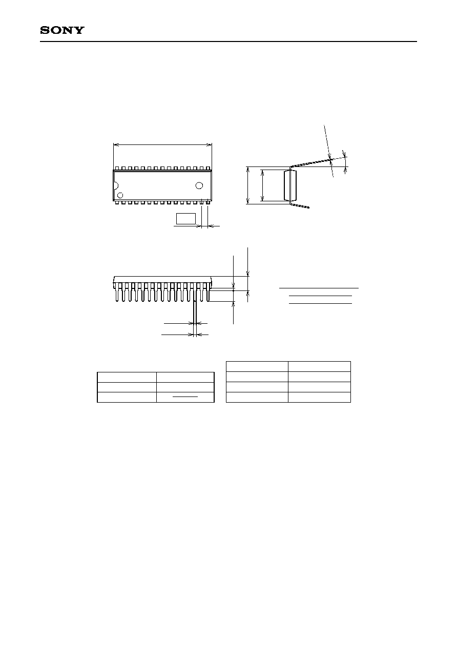
Package Outline
Unit: mm
SONY CODE
EIAJ CODE
JEDEC CODE
30PIN SDIP (PLASTIC)
26.9 ≠ 0.1
+ 0.4
15
16
30
1.778
10.16
8.5
≠
0.1
+ 0.3
0.25
≠
0.05
+ 0.1
0
∞
to 15
∞
0.5
±
0.1
0.9
±
0.15
3.0 MIN
0.5 MIN
3.7
≠
0.1
+ 0.4
SDIP-30P-01
P-SDIP30-8.5x26.9-1.778
1
PACKAGE STRUCTURE
MOLDING COMPOUND
LEAD TREATMENT
LEAD MATERIAL
PACKAGE MASS
EPOXY RESIN
COPPER ALLOY
1.8g
PALLADIUM PLATING
1.All mat surface type.
Two kinds of package surface:
2.All mirror surface type.
Sony Corporation