 | –≠–ª–µ–∫—Ç—Ä–æ–Ω–Ω—ã–π –∫–æ–º–ø–æ–Ω–µ–Ω—Ç: CXA2509 | –°–∫–∞—á–∞—Ç—å:  PDF PDF  ZIP ZIP |

≠ 1 ≠
CXA2509AQ
E96826-PS
Playback Equalizer Amplifier with Music Sensor
Description
The CXA2509AQ is an IC designed for use in car
stereo cassette decks. Functions include playback
equalizer amplifier and music sensor into a single
chip.
Features
∑ Few external parts
∑ Small package (40-pin QFP)
∑ Same pin configuration as for the Dolby B-C type
NR system (CXA2511AQ) and Dolby B type NR
system (CXA2510AQ)
∑ Playback equalizer amplifier and music sensor into
a single chip
∑ FORWARD/REVERSE head select switch
∑ Two-system (TAPE/AUX) input select switch
∑ Music signal interval detection level can be set by
the external resistors/capacitors (2 modes).
∑ High-frequency cut-off of the music sensor circuit
can be adjusted by the external capacitance.
Applications
∑ Car stereo cassette decks
∑ Playback-only cassette decks
Structure
Bipolar silicon monolithic IC
Absolute Maximum Ratings
∑ Supply voltage
V
CC
12
V
∑ Operating temperature Topr
≠40 to +85
∞C
∑ Storage temperature
Tstg
≠65 to +150
∞C
∑ Power dissipation
P
D
430
mW
Operating Condition
Supply voltage
V
CC
7.8 to 11
V
Sony reserves the right to change products and specifications without prior notice. This information does not convey any license by
any implication or otherwise under any patents or other right. Application circuits shown, if any, are typical examples illustrating the
operation of the devices. Sony cannot assume responsibility for any problems arising out of the use of these circuits.
40 pin QFP (Plastic)
≠ 2 ≠
CXA2509AQ
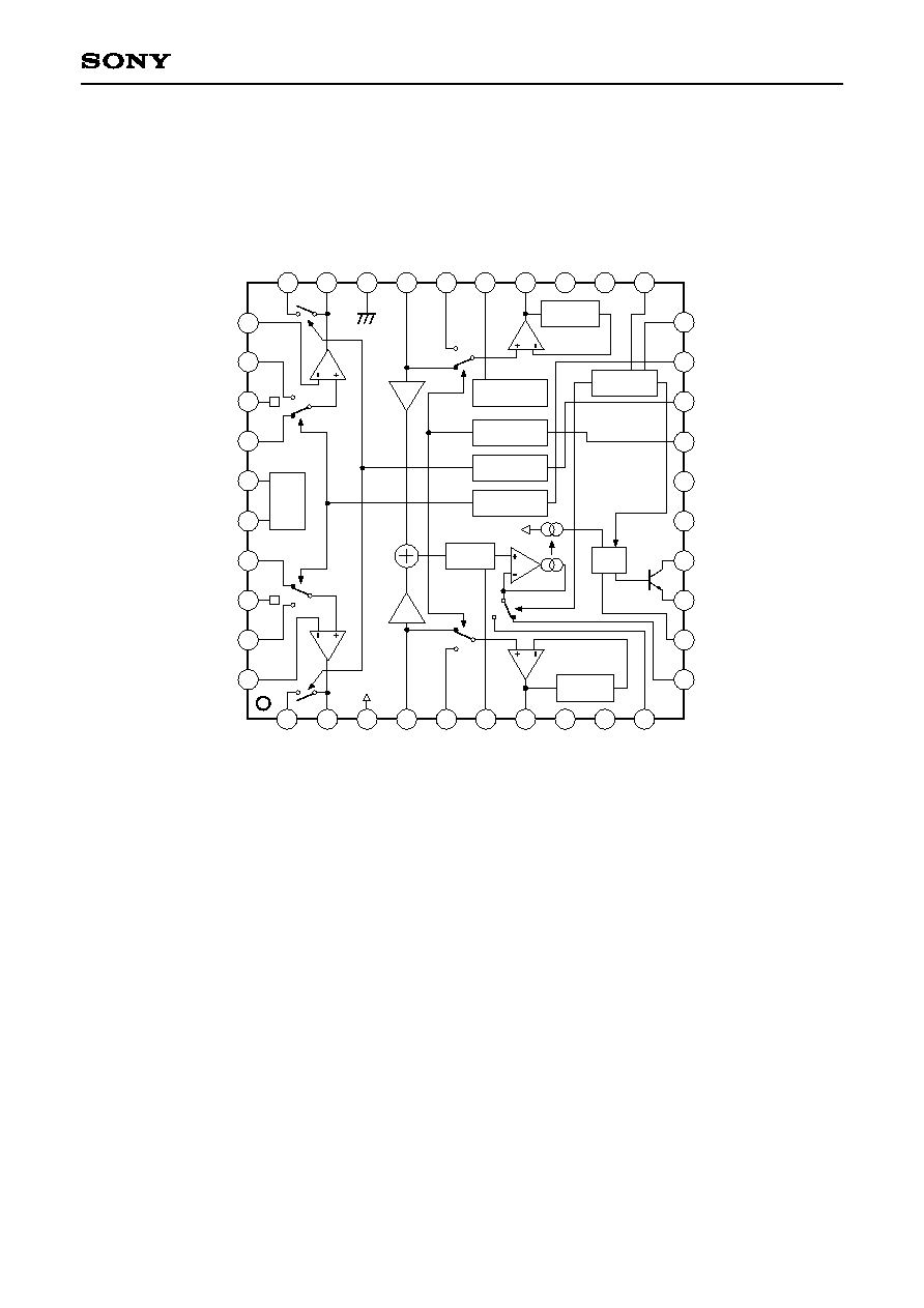
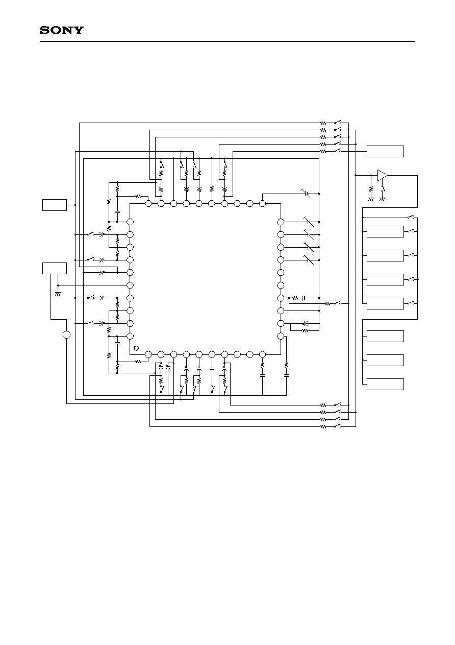
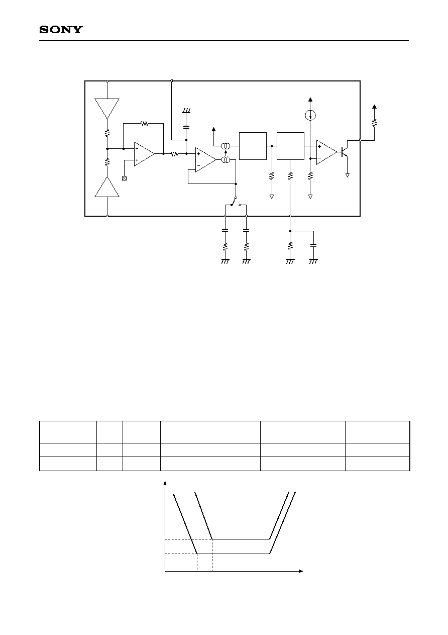
Block Diagram and Pin Configuration
NR BIAS
FWD/RVS
◊
1
24dB
TAPE/AUX
TAPE EQ
MS MODE
DET
24dB
LPF
◊
1
VCT
V
CC
T2
MS ON/
OFF
F3
T1
120µ/70µ
120µ/70µ
F2
F1
21
22
23
24
25
26
27
28
29
30
40
39
38
37
36
35
34
31
32
33
11
12
13
14
15
16
17
18
19
20
2
3
4
5
6
7
8
9
10
1
PBFB2
PBRIN2
PBREF2
PBFIN2
VCT
PBGND
PBFIN1
PBREF1
PBRIN1
PBFB1
PBEQ2
PBOUT2
TAPEIN2
GND
AUXIN2
DIREF
NC
LINEOUT2
NC
MSSW
MSMODE
DRSW
TAPESW
INSW
NC
NC
MSOUT
DGND
MSTC
G1FB
PBEQ1
PBOUT1
TAPEIN1
V
CC
AUXIN1
MSLPF
NC
LINEOUT1
NC
G2FB
≠ 3 ≠
CXA2509AQ
Pin Description
(Ta = 25∞C, V
CC
= 8.0V, DV
CC
= 5.0V)
Pin
No.
Symbol
Typical pin voltage
I/O
I/O
resistance
Equivalent circuit
Description
DC
AC
1
30
PBEQ1
PBEQ2
O
--
Resistance for
selecting the
playback equalizer
amplifier time
constant
4.0V
--
30
1
GND
1k
40k
1k
5k
Vcc
2
29
PBOUT1
PBOUT2
O
--
Playback
equalizer amplifier
output
4.0V
≠25dBm
3
V
CC
--
--
Power supply
8.0V
--
2
29
GND
200
200
Vcc
4
27
TAPEIN1
TAPEIN2
I
40k
TAPE input
5
26
AUXIN1
AUXIN2
External input
4.0V
≠30dBm
4
5
26
27
GND
147
40k
Vcc
VGS
20p
6
MSLPF
--
100k
Cut-off frequency
adjustment of the
music sensor LPF
4.0V
--
6
GND
147
Vcc
64p
100k
≠ 4 ≠
CXA2509AQ
7
24
LINEOUT1
LINEOUT2
O
--
Line output
4.0V
≠6dBm
10
11
G2FB
G1FB
--
--
Music signal
interval detection
level setting
4.0V
--
12
MSTC
--
--
Time constant for
detecting the
music signal
interval
--
--
13
DGND
--
--
Logic ground
(Connect to GND.)
0.0V
--
7
24
GND
200
200
Vcc
22.5k
147
11
GND
500
Vcc
147
10
500
12
GND
147
10k
Vcc
DGND
853
14
MSOUT
O
--
Music sensor
output
0.2V
when a
signal is
detected;
DVcc
when no
signal is
detected
--
GND
Vcc
DGND
14
DVcc
100k
Pin
No.
Symbol
Typical pin voltage
I/O
I/O
resistance
Equivalent circuit
Description
DC
AC
≠ 5 ≠
CXA2509AQ
17
Line amplifier input
select control
Low (open): TAPEIN
High: AUXIN
18
TAPESW
Playback equalizer
amplifier control
Low (open): 120µs
High: 70µs
19
DRSW
Head select control
Low (open):
FORWARD
High: REVERSE
INSW
19
GND
100k
Vcc
1.1k
DGND
18
17
I
100k
0.0V
when
open
--
21
MSSW
Music sensor
control
Low (open): MS ON
High: MS OFF
I
100k
0.0V
when
open
--
20
MSMODE
I
100k
Music sensor
mode control
Low (open): G1
High : G2
0.0V
when
open
--
GND
100k
Vcc
1.1k
DGND
20
GND
100k
Vcc
1.1k
DGND
21
Pin
No.
Symbol
Typical pin voltage
I/O
I/O
resistance
Equivalent circuit
Description
DC
AC
≠ 6 ≠
CXA2509AQ
25
DIREF
--
--
Resistance for
setting the
reference current
(Connects
20 (18) k
between DIREF
pin and GND for
the standard
setting.)
1.2V
--
Vcc
147
25
GND
40
36
34
31
32
Vcc
GND
39
PBREF
PBREF
50p
50p
28
GND
--
--
Ground
0.0V
--
31
40
PBFB2
PBFB1
I
--
Playback
equalizer amplifier
feedback
4.0V
≠70dBm
32
39
PBRIN2
PBRIN1
Playback
equalizer amplifier
input (REVERSE
head connected)
34
37
PBFIN2
PBFIN1
I
--
Playback
equalizer amplifier
input (FORWARD
head connected)
4.0V
≠70dBm
33
38
PBREF2
PBREF1
O
--
Playback
equalizer amplifier
reference (V
CC
/2
output)
4.0V
--
38
33
GND
200
Vcc
200
Pin
No.
Symbol
Typical pin voltage
I/O
I/O
resistance
Equivalent circuit
Description
DC
AC
≠ 7 ≠
CXA2509AQ
35
VCT
O
--
Center (V
CC
/2
output)
4.0V
--
35
GND
45k
Vcc
147
◊
1
30k
30k
VGS
36
PBGND
--
--
Playback
equalizer amplifier
ground (Connect
to ground.)
0.0V
--
8
9
15
16
22
23
NC
--
--
No connected
--
--
Pin
No.
Symbol
Typical pin voltage
I/O
I/O
resistance
Equivalent circuit
Description
DC
AC
≠ 8 ≠
CXA2509AQ
Vopr
I
CC
V
TIN
V
AUX
THD1
SN1
SH1
CT1
CT2
CT3
V
OS
1
PBREF
F120
F70
SH2
THD2
SN2
V
OS
2
CT4
CT5
Playback Equalizer Amplifier
Electrical Characteristics
(Ta = 25∞C, V
CC
= 8.0V, DV
CC
= 5.0V)
Item
Symbol
Measurement conditions
No signal, TAPE, 120µs, MS ON
TAPEIN 1kHz, LINEOUT 0dB
AUXIN 1kHz, LINEOUT 0dB
TAPEIN 1kHz ≠20dBm, RL = 2.7k
No signal, Rg = 5.1k
,
CCIR/ARM filter used
TAPEIN 1kHz, RL = 2.7k
, THD = 1%
TAPEIN 1kHz ≠24dBm, 1kHz BPF used
AUXIN 1kHz ≠24dBm, 1kHz BPF used
TAPE (AUX) IN 1kHz ≠24dBm,
AUX (TAPE) mode, 1kHz BPF used
1
No signal, NR OFF, difference from VCT
PBIN 315Hz ≠70dBm, 120µs mode
PBIN 2.7kHz ≠58.5dBm,
120µs mode at 315Hz
PBIN 4.5kHz ≠53.8dBm,
70µs mode at 315Hz
PBIN 1kHz, 120µs mode, RL = 2.7k
,
THD = 1%
PBIN 1kHz ≠52dBm, 120µs mode,
RL = 2.7k
No signal, 70µs mode, Rg = 680
,
CCIR/ARM filter used
No signal, 120µs mode, Rg = 680
,
difference from VCT
PBIN 1kHz ≠52dBm, 120µs mode,
1kHz BPF used
PBIN 1kHz ≠52dBm, 120µs mode,
1kHz BPF used
7.8
5.3
≠32.0
≠32.0
--
74.0
13.0
--
--
--
≠0.1
≠27.0
≠1.5
≠1.5
≠10.0
--
59.0
≠1.0
--
--
8.0
7.8
≠30.0
≠30.0
0.01
79.4
14.4
≠86.0
≠86.0
≠67.0
0.0
≠25.0
0.0
0.0
≠3.0
0.07
64.5
0.0
≠81.0
≠80.0
11.0
10.3
≠28.0
≠28.0
0.2
--
--
≠70.0
≠70.0
≠65.0
0.1
≠23.0
1.5
1.5
--
0.5
--
1.0
≠70.0
≠70.0
V
mA
dBm
dBm
%
dB
dB
dB
dB
dB
V
dBm
dB
dB
dBm
%
dB
V
dB
dB
Operating voltage
Current consumption
TAPEIN input sensitivity
AUXIN input sensitivity
Total harmonic distortion
S/N ratio
Signal handling
Crosstalk between
channels 1
Crosstalk between
channels 2
Crosstalk between
TAPE and AUX
Output DC offset voltage
Playback equalizer amplifier
reference output level
Playback equalizer amplifier
frequency response 1
Playback equalizer amplifier
frequency response 2
Signal handling
Total harmonic
distortion
S/N ratio
Output DC offset
voltage
Crosstalk between
channels
Crosstalk between
FORWARD and REVERSE
Line Amplifier (0dB = Line amplifier reference output level LINEOUT of ≠6dBm)
Min.
Typ.
Max.
Unit
≠ 9 ≠
CXA2509AQ
Item
Symbol
Measurement conditions
Min.
Typ.
Max.
Unit
V
MS
1
V
MS
2
I
OH
V
OL
V
IL
V
IH
TAPEIN 5kHz, MS ON, G1 mode,
external constant of 39k
and 0.0047µF
TAPEIN 5kHz, MS ON, G2 mode,
external constant of 3.9k
and 0.47µF
No signal, MS OFF, G1 mode
TAPEIN 5kHz ≠30dBm, MS ON,
G1 mode, 1mA applied to MSOUT pin
Input voltage of INSW, TAPESW, DRSW,
MSMODE, MSSW
Input voltage of INSW, TAPESW, DRSW,
MSMODE, MSSW
≠43.0
≠63.0
--
--
0.0
2.5
≠40.0
≠60.0
0.0
0.3
--
--
≠37.0
≠57.0
1.0
1.0
0.5
DV
CC
dBm
dBm
µA
V
V
V
Signal detection level 1
Signal detection level 2
MS output leak current
MS output saturation
voltage
Logic Voltage
Low level
High level
Music Sensor
1
The crosstalk between TAPE and AUX is measured with a 5.1k
external resistor connected to AUXIN1
(Pin 5). In this condition, the crosstalk is approximately ≠67dB due to the signal leak from MSLPF (Pin 6).
In order to improve the crosstalk between TAPE and AUX, AUXIN1 pin should be driven with a low
impedance.
≠ 10 ≠
CXA2509AQ
Electrical Characteristics Measurement Circuit
Audio
SG
PBFB2
PBRIN2
PBREF2
PBFIN2
VCT
PBGND
PBFIN1
PBREF1
PBRIN1
PBFB1
PBEQ2
PBOUT2
TAPEIN2
GND
AUXIN2
DIREF
NC
LINEOUT2
NC
MSSW
MSMODE
DRSW
TAPESW
INSW
NC
NC
MSOUT
DGND
MSTC
G1FB
PBEQ1
PBOUT1
TAPEIN1
V
CC
AUXIN1
MSLPF
NC
LINEOUT1
NC
G2FB
V
CC
R11
18k
C11
1µ
C13
1µ
C15
270p
C16
2.2µ
C18
0.47µ
C19
4.7n
R22
3.9k
R23
39k
C9
2.2µ
C17
2.2µ
GND
21
22
23
24
25
26
27
28
29
30
40
39
38
37
36
35
34
31
32
33
11
12
13
14
15
16
17
18
19
20
2
3
4
5
6
7
8
9
10
1
C20
0.1µ
R25
1MEG
R24
100k
A
R30
10k S18
INSW
H/L
TAPESW
H/L
DRSW
H/L
MSMODE
H/L
MSSW
H/L
DV
CC
R5
12k
Power
Supply
DC Ammeter
GND GND
CCIR/ARM
"A" WTG
DIN Audio
1kHz BPF
DC
Voltmeter
0dB or 30dB
Amp
OFF: 0dB
ON: 30dB
R36
50k
S24
S29
S28
S27
S26
S25
+20dB
+20dB
AC
Voltmeter
Distortion
Analyzer
Oscilloscope
S23
S22
S21
S20
S19
R35 10k
R34 100
R33 10k
R32 100
R31 10k
S17
S16
S15
S14
R29 10k
R28 100
R27 10k
R26 100
R20 2.7k
S12
S11
S8
S7
R17 5.1k
R15 5.1k
R13 2.7k
S5
C8
2.2µ
C10 22µ
C6
0.01µ
R1
300k
S1
C1
2.2µ
R2
270
R6
680
R7
680
S2
C2
2.2µ
C3
22µ
S3
C4
2.2µ
R9
680
R8
680
S4
C5
2.2µ
C7
0.01µ
R12
18k
R10
12k
R4
300k
R3
270
C12
1µ
C14
1µ
R19
20k
R14
2.7k
R16 5.1k
R18 5.1k
R21 2.7k
S8
S10
S13
S6
:
Note 1. Resistor tolerance
2. Capacitor tolerance
Coupling Capacitor
±5%
±1%
±5%
±2%
±10%
:

≠ 11 ≠
CXA2509AQ
Application Circuit 1
NR BIAS
FWD/RVS
◊
1
24dB
TAPE/AUX
TAPE EQ
MS MODE
24dB
LPF
◊
1
VCT
V
CC
T2
F3
T1
120µ/70µ
120µ/70µ
F2
F1
C4
470p
C3
470p
R3
100k
R4
100k
PBFB2
PBRIN2
PBEQ2
PBOUT2
TAPEIN2
MSMODE
R11
12k
R9
18k
R12
300k
GND
PBREF2
PBFIN2
VCT
PBGND
PBFIN1
PBREF1
PBRIN1
PBFB1
GND
AUXIN2
DIREF
NC
LINEOUT2
NC
MSSW
DRSW
TAPESW
INSW
NC
NC
MSOUT
DGND
MSTC
G1FB
PBEQ1
PBOUT1
TAPEIN1
V
CC
AUXIN1
MSLPF
NC
LINEOUT1
NC
G2FB
RVS2
FWD2
C5
22µ
FWD1
RVS1
C2
470p
C1
470p
R1
100k
R2
100k
R5
180
C6
0.01µ
R10
12k
R7
300k
R8
18k
AUXIN1
C8
22µ
V
CC
GND
LINEOUT1
GND
GND
GND
C9
2.2µ
C11
2.2µ
C13
0.001µ
C14
2.2µ
C16
0.47µ
C17
4.7n
R16
3.9k
R17
39k
C7
0.01µ
C10
2.2µ
C12
2.2µ
C15
2.2µ
C17
0.1µ
R15
20k
LINEOUT2
GND
AUXIN2
21
22
23
24
25
26
27
28
29
30
40
39
38
37
36
35
34
31
32
33
11
12
13
14
15
16
17
18
19
20
2
3
4
5
6
7
8
9
10
1
C18
0.1µ
R18
1MEG
R19
100k
To Microcomputer
DV
CC
DGND
From
Microcomputer
GND
GND
R14
33k
R13
33k
R6
180
DET
MS ON/
OFF
GND
Application circuits shown are typical examples illustrating the operation of the devices. Sony cannot assume responsibility for
any problems arising out of the use of these circuits or for any infringement of third party patent and other right due to same.

≠ 12 ≠
CXA2509AQ
Application Circuit 2
NR BIAS
FWD/RVS
◊
1
24dB
TAPE/AUX
TAPE EQ
MS MODE
24dB
LPF
◊
1
VCT
V
CC
T2
F3
T1
120µ/70µ
120µ/70µ
F2
F1
C1
470p
C2
470p
R2
100k
R1
R5
500
PBFB2
PBRIN2
PBEQ2
PBOUT2
TAPEIN2
MSMODE
R11
12k
R9
18k
R12
300k
GND
PBREF2
PBFIN2
VCT
PBGND
PBFIN1
PBREF1
PBRIN1
PBFB1
GND
AUXIN2
DIREF
NC
LINEOUT2
NC
MSSW
DRSW
TAPESW
INSW
NC
MSOUT
DGND
MSTC
G1FB
PBEQ1
PBOUT1
TAPEIN1
V
CC
AUXIN1
MSLPF
NC
LINEOUT1
NC
G2FB
RVS2
FWD2
C5
22µ
FWD1
RVS1
C3
470p
C4
470p
R3
100k
R6
500
C6
0.01µ
R10
12k
R7
300k
R8
18k
AUXIN1
C8
22µ
V
CC
GND
LINEOUT1
GND
GND
GND
C9
2.2µ
C11
2.2µ
C13
0.001µ
C14
2.2µ
C16
0.47µ
C17
4.7n
R14
3.9k
R15
39k
C7
0.01µ
C10
2.2µ
C12
2.2µ
C15
2.2µ
R13
20k
LINEOUT2
GND
AUXIN2
21
22
23
24
25
26
27
28
29
30
40
39
38
37
36
35
34
31
32
33
11
12
13
14
15
16
17
18
19
20
2
3
4
5
6
7
8
9
10
1
C18
0.1µ
R16
1MEG
R17
100k
To Microcomputer
DV
CC
DGND
From
Microcomputer
GND
GND
DET
MS ON/
OFF
100k
R4 100k
NC
GND
Application circuits shown are typical examples illustrating the operation of the devices. Sony cannot assume responsibility for
any problems arising out of the use of these circuits or for any infringement of third party patent and other right due to same.
≠ 13 ≠
CXA2509AQ
Description of Operation
1. Signal route
AUX
TAPE
TAPEIN
(≠30dBm)
AUXIN
PBFB
PBEQ
AMP1
24dB
24dB
AMP2
PBOUT
LINEOUT
(≠6dBm line amplifier reference output level)
70µs
FWD
RVS
PB IN
Fig. 1. Signal route block diagram
AMP1 and AMP2 are operational amplifiers. AMP1 composes the playback equalizer amplifier by attaching an
external resistor and capacitor to PBFB, PBEQ and PBOUT pins.
AMP2 is an input selector and a line amplifier. The gain is 24dB.
The line amplifier reference output level is ≠6dBm.
≠ 14 ≠
CXA2509AQ
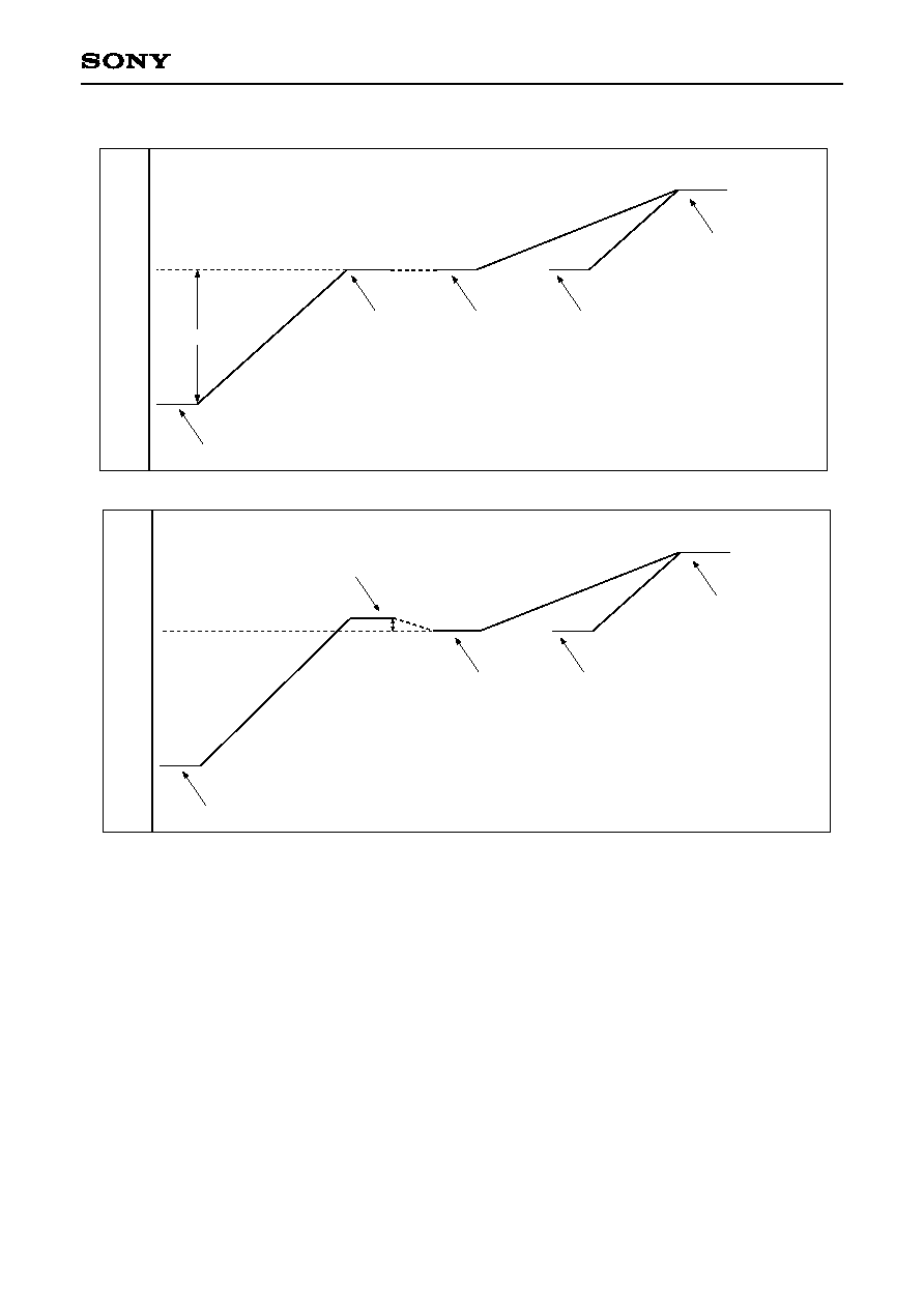
2. Adjustment method
0
≠10
(dBm)
LINEOUT
≠30dBm
400Hz 200nWb/m: Dolby level reference tape
PBIN (HEAD)
AUXIN
TAPEIN
PBOUT
≠30dBm
≠6dBm
(Dolby level)
≠80
≠30
≠40
≠50
≠60
≠70
≠20
VR adjustment
Fig. 2-1. Level diagram (application circuit 1)
0
≠10
(dBm)
LINEOUT
≠30dBm
400Hz 200nWb/m: Dolby level reference tape
PBIN (HEAD)
AUXIN
TAPEIN
PBOUT
≠30dBm
≠6dBm
(Dolby level)
≠80
≠30
≠40
≠50
≠60
≠70
≠20
VR adjustment
Fig. 2-2. Level diagram (application circuit 2)
As an example of the playback equalizer gain adjustment method, the reference tape for Dolby level
adjustment is playd back in order to obtain ≠6dBm output on LINEOUT (Pins 7 and 24).
The same output level as for ICs with the built-in Dolby NR system(CXA2510AQ and CXA2511AQ) can be
obtained.
List of Calibration Cassette Tape
Dolby level is defined as 200nWb/m measured according to the ANSI high efficiency head method.
The followings are the reference tapes specified by Dolby Laboratories Licensing Corporation.
1. A-bex Laboratories, Inc. (part no. TCC-130)
2. BASF (product code 09797 XE)
3. Kaneon Corp. (LC Engineering part no. LCT-7001)
4. Standard Tape Laboratory (catalogue no. 28)
5. TEAC Corporation, Japan (part no. MTT150)
6. TEAC Corporation of America (part no. MTT150)
7. Victor Company of Japan, Ltd. (part no. TMT-6130, VTT-727)
8. Sony Corporation (part no. TY-256)
≠ 15 ≠
CXA2509AQ
PBFB
PBEQ
AMP1
PBOUT
70µs
FWD
RVS
PB IN
PBREF
R1
R2
R3
R4
C1
SW2
SW1
≠6dB/oct
T3
Gain (dB)
G1
f3
f2
f1
Frequency (Hz)
T2
T1
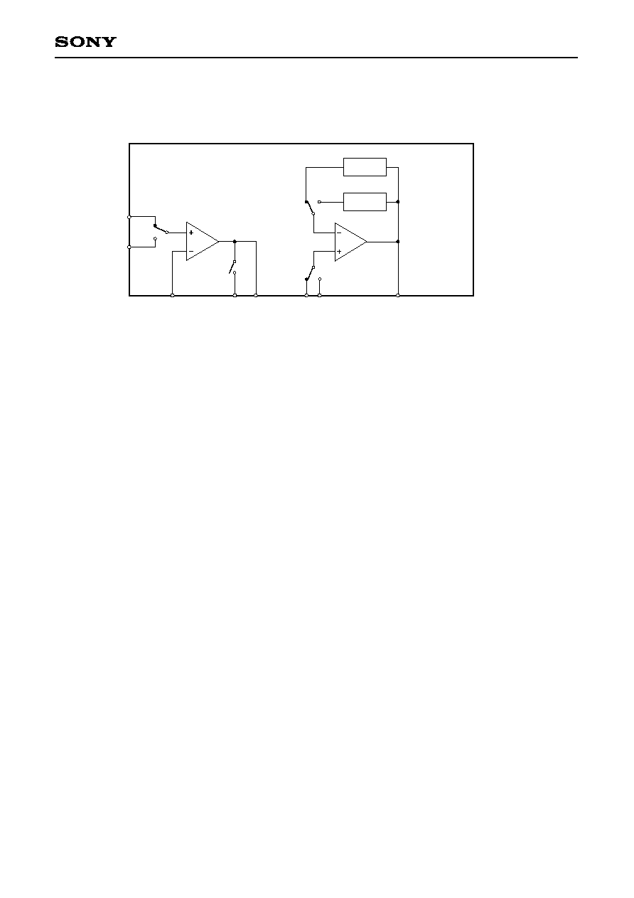
3. Playback equalizer amplifier
Fig. 3. Playback equalizer amplifier
block diagram
Fig. 4. Playback equalizer amplifier
frequency response
The CXA2509AQ achieves the frequency response of Fig.4 with the circuit configuration shown in Fig. 3.
Two systems (FORWARD and REVERSE) of playback head input are provided for each channel.
The FORWARD input pin is selected when DRSW (Pin 19) is Low; REVERSE is selected when DRSW is
High.
The playback equalizer amplifier frequency response can be set in two levels.
When TAPESW (Pin 18) is Low, SW2 shown in Fig. 3 is turned OFF; when TAPESW is High, SW2 is turned
ON.
The external resistance R1 should be adjusted to adjust the playback equalizer amplifier gain.
The playback equalizer amplifier frequency response is all determined by the external resistance and
capacitance, and it can be obtained with the following equation.
G (s) = ∑ (s = j
)
Where, Rx = R3 when TAPESW pin = Low;
Rx = R3//R4 when TAPESW pin = High
Using the above equation, G1 in Fig. 3 and low-frequency time constant (T1) and high-frequency time
constants (T2 and T3) are as follows:
G1 = 20log
T1 = C1 ∑ (R2 + Rx)
T2, T3 =
R1 + R2
R1
C1 ∑ (R1 ∑ R2 + R2 ∑ Rx + Rx ∑ R1)
R1 + R2
R1 + R2
R1
1 + {s ∑ C1 ∑ (R1 ∑ R2 + R2 ∑ Rx + Rx ∑ R1) / (R1 + R2)}
1 + s ∑ C1 ∑ (R2 + Rx)
≠ 16 ≠
CXA2509AQ
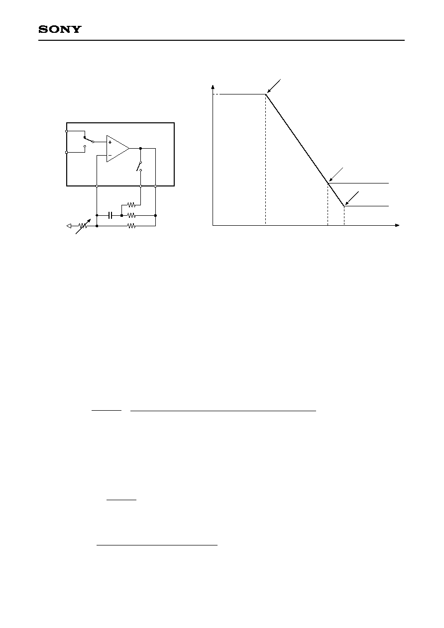
4. Music sensor
AMP2
TAPEIN2
AMP3
AMP1
Full-wave
rectifier
Smoother
Vcc
Vcc
MSLPF
◊
1
R1
10k
VGS
R2
10k
R3
127k
◊
1
R5
39.1k
C1
64p
R6
1k
R7
11.1k
DVcc
R11
MSOUT
MSTC
R10
C4
G2FB
R9
C3
G1FB
R8
C2
TAPEIN1
R4
100k
DGND
DGND
DGND
Fig. 5. Music sensor block diagram
The signal input from TAPEIN is added and amplified by AMP1.
This signal is then input to the LPF (R4 and C1). The LPF cut-off frequency can be adjusted by connecting the
external capacitance to MSLPF pin. The cut-off frequency is approximately 23kHz when MSLPF pin is left
open.
The detection level and HPF cut-off frequency are determined with the external resistance and capacitance
connected to G1FB or G2FB at AMP2, and the signal is converted to a current.
The signal is full-wave rectified and is converted to a voltage by the internal resistance R5.
The full-wave rectified signal is smoothed. The internal resistance (R6) and external capacitance (C4)
determine the smoothing response time. The recovery time is determined by the external resistance (R10) and
capacitance (C4).
The AMP3 comparator detects whether the smoothed signal is greater or smaller than the comparator
threshold.
The comparator has approximately 2dB hysteresis.
The table below shows the example of the constant and characteristics for the external resistance and
capacitance connected to G1FB and G2FB.
R
C
Music signal detection level
Music signal interval
detection level
Cut-off frequency
FF/REW (G1)
Playback (G2)
39k
3.9k
0.0047µF
0.47µF
≠39.5dBm
≠59.5dBm
≠41.4dBm
≠61.4dBm
870Hz
87Hz
Detection level
(dBm)
≠39.5
G1 (FF)
870
87
Frequency (Hz)
≠59.5
G2 (NOR)
Fig. 6. Music sensor circuit frequency response
≠ 17 ≠
CXA2509AQ
5. Operating mode control method
The CXA2509AQ has a playback equalizer amplifier select switch (TAPESW), head input select switch
(DRSW), music sensor mode select switch (MSMODE) and music sensor switch (MSSW).
The operating modes for each switch are shown in the following table.
Low (OPEN)
High
TAPE
120µs
PBIN FORWARD
G1
MS ON
17
18
19
20
21
INSW
TAPESW
DRSW
MSMODE
MSSW
AUX
70µs
PBIN REVERSE
G2
MS OFF
Pin voltage
Pin No.
Pin name
Notes on Operation
1. Playback equalizer amplifier
All playback equalizer amplifier characteristics are determined by the external constants. Use the parts
which satisfies the accuracy required for the playback equalizer amplifier.
2. Music sensor
The current on DIREF (Pin 25), and the resistance and capacitance connected to G2FB (Pin 10) and G1FB
(Pin 11) determine the detection level and the HPF cut-off frequency.
The response time is determined by the resistance and capacitance connected to MSTC (Pin 12).
Use the parts which satisfies the accuracy required for the music sensor.
≠ 18 ≠
CXA2509AQ
Example of Representative Characteristics
Current consumption vs. Supply voltage
8.0
7.5
7.0
7.0
8.0
9.0
10.0
11.0
Ta = 25∞C
Supply voltage [V]
Current consumption [mA]
No input signal
MS ON
Playback equalizer amplifier frequency response
100
1k
10k
Frequency [Hz]
30
40
50
Gain [dB]
60
V
CC
= 8.0V
Output level of ≠25dBm constant
120µs
Ta = 25∞C
70µs
Line amplifier frequency response
30
20
10
100
1K
10K
Frequency [Hz]
Gain [dB]
Ta = 25∞C
V
CC
= 8.0V
Input: TAPE IN1
AUX IN1
Output: LINE OUT1
PBFIN1
PBREF
680
70µs
PBOUT1
PBEQ1
18k
12k
300k
0.01µ
2.2µ
270
PBREF
PBFB1
47µ
Fig. 7. Measurement circuit of playback
equalizer amplifier frequency response
≠ 19 ≠
CXA2509AQ
Total harmonic distortion (playback equalizer amplifier)
≠20
≠16 ≠12
≠8
≠4
0
4
8
Output level [dBm]
10
≠2
10
≠1
10
0
Total harmonic distortion [%]
Ta = 25∞C
f = 10kHz
f = 100Hz
f = 1kHz
V
CC
= 8.0V
Input: PBFIN1
Output: PBOUT1
R
L
= 2.7k
Total harmonic distortion (line amplifier)
≠10
≠6
≠2
2
6
10
14
Output level [dB]
10
≠2
10
≠1
10
0
Total harmonic distortion [%]
f = 10kHz
f = 100Hz
f = 1kHz
Ta = 25∞C
V
CC
= 8.0V
Input: TAPEIN1
Output: LINEOUT1
R
L
= 2.7k
0dB = ≠6dBm
Ripple rejection ratio (PBOUT)
100
1k
10k
Frequency [Hz]
≠60
≠50
≠40
Ripple rejection ratio [dB]
Ta = 25∞C
V
CC
= 8.0V
R
L
= 2.7k
Ripple rejection ratio (LINEOUT)
100
1k
10k
Frequency [Hz]
≠40
≠30
≠20
Ripple rejection ratio [dB]
≠50
Ta = 25∞C
V
CC
= 8.0V
R
L
= 2.7k
≠ 20 ≠
CXA2509AQ
Crosstalk between channels (1ch
2ch)
100
10k
Frequency [Hz]
≠60
≠40
0
Crosstalk [dB]
≠120
≠20
≠80
≠100
V
CC
= 8.0V
Input: PBFIN1
Output: LINEOUT2
(constant LINEOUT level)
1k
V
CC
= 8.0V
Input: TAPEIN1
G1: R = 39k
, C = 4.7nF
G2: R = 3.9k
, C = 0.47µF
Music signal and signal interval detection level
frequency response
100
1k
10k
Frequency [Hz]
≠40
≠10
0
Input level [dBm]
≠60
≠20
≠30
≠50
Music signal interval detection level
Ta = 25∞C
Music signal detection level
Music signal interval detection level
Music signal detection level G2
G1
Ta = 25∞C
HPF connection resistance in MS block vs.
Music signal and signal interval detection level characteristics
1k
10k
100k
HPF connection resistance [
]
≠50
≠40
≠30
Input level [dBm]
≠60
Music signal interval
detection level
≠70
V
CC
= 8.0V
f = 5kHz
Input: TAPEIN1
Music signal
detection level
PBFIN1
PBREF
680
PBOUT1
PBEQ1
270
PBREF
47µ
12k
300k
24dB
TAPEIN1
LINEOUT1
2.2µ
Fig. 8. Measurement circuit of crosstalk
between channels
≠ 21 ≠
CXA2509AQ
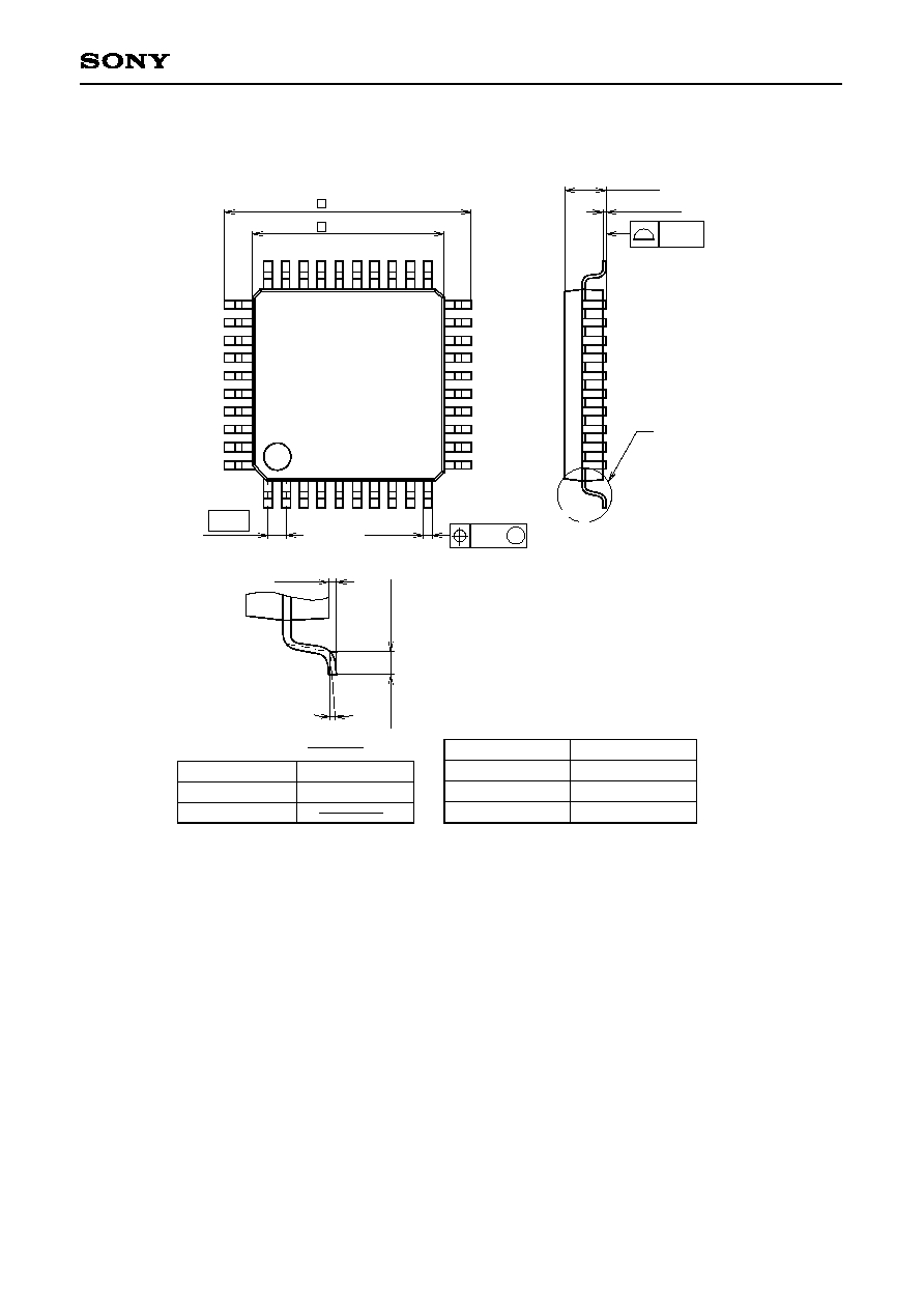
Package Outline
Unit: mm
SONY CODE
EIAJ CODE
JEDEC CODE
PACKAGE MATERIAL
LEAD TREATMENT
LEAD MATERIAL
PACKAGE MASS
EPOXY RESIN
SOLDER / PALLADIUM
42/COPPER ALLOY
PACKAGE STRUCTURE
PLATING
0.2g
QFP-40P-L01
QFP040-P-0707
40PIN QFP (PLASTIC)
9.0 ± 0.4
+ 0.4
0.3 ≠ 0.1
1
10
11
20
21
30
31
40
1.5 ≠ 0.15
+ 0.35
0.127 ≠ 0.05
+ 0.1
(8.0)
A
A
DETAIL
0.1 ≠ 0.1
+ 0.15
+ 0.15
7.0 ≠ 0.1
0.5 ±
0.2
0.1
M
± 0.12
0.65
NOTE : PALLADIUM PLATING
This product uses S-PdPPF (Sony Spec.-Palladium Pre-Plated Lead Frame).