 | –≠–ª–µ–∫—Ç—Ä–æ–Ω–Ω—ã–π –∫–æ–º–ø–æ–Ω–µ–Ω—Ç: CXA3099N | –°–∫–∞—á–∞—Ç—å:  PDF PDF  ZIP ZIP |

--1--
E95Y24A8Z
Sony reserves the right to change products and specifications without prior notice. This information does not convey any license by
any implication or otherwise under any patents or other right. Application circuits shown, if any, are typical examples illustrating the
operation of the devices. Sony cannot assume responsibility for any problems arising out of the use of these circuits.
Absolute Maximum Ratings
∑ Supply voltage
V
CC
7.0
V
∑ Operating temperature
Topr
≠20 to +75 ∞C
∑ Storage temperature
Tstg ≠65 to +150 ∞C
∑ Allowable power dissipation P
D
312
mW
Operating Condition
Supply voltage
V
CC
1
1.1 to 4.0
V
Description
The CXA3099N is a low current consumption FM
IF amplifier which employs the newest bipolar
process. It is suitable for M-ary FSK pagers.
Features
∑ Low current consumption: 590 µA
(typ. at V
CC
= 1.4 V)
∑ Low voltage operation: V
CC
= 1.1 to 4.0 V
∑ Small package 16-pin SSOP
∑ Needless of IF decoupling capacitor
∑ Reference power supply for operational amplifier
and comparator
∑ IF input, V
CC
standard
Applications
M-ary FSK pagers
Structure
Bipolar silicon monolithic IC
IF Amplifier for M-ary FSK Pagers
16 pin SSOP (Plastic)
CXA3099N
For the availability of this product, please contact the sales office.

--2--
CXA3099N
R
S
S
I
D
E
V
C
O
M
P
V
C
C
R
E
G
O
U
T
R
E
G
C
O
N
T
L
V
A
O
U
T
N
R
Z
O
U
T
C
H
A
R
G
E
D
E
V
O
U
T
R
S
S
I
L
P
F
O
U
T
L
P
F
I
N
D
E
T
O
U
T
Q
U
A
D
F
S
K
R
E
F
B
S
G
N
D
I
F
I
N
78
k
R2
22
k
R1
G
N
D
R
E
G
I
F
L
I
M
1
0
1
1
1
2
1
3
1
4
1
6
9
1
5
2
3
4
5
6
7
1
8
C
H
A
R
G
E
Q
U
A
D
D
E
T
V
B
R
E
G
N
R
Z
C
O
M
P
L
V
A
Block Diagram and Pin Configuration
--3--
CXA3099N
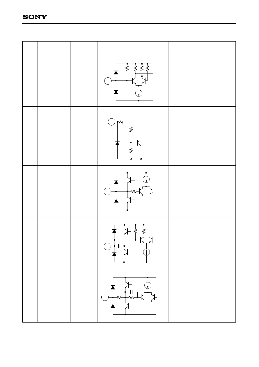
Pin Description
Pin
No.
Symbol
Pin voltage
Equivalent circuit
Description
1
2
3
4
5
6
IF IN
GND
B.S.
FSK REF
QUAD
DET OUT
1.4 V
--
--
0.2 V
1.4 V
0.2V
IF limiter amplifier input.
Ground.
Controls the battery saving.
Setting this pin low suspends the
operation of IC. (Applied voltage
range: ≠0.5 V to +7.0 V)
Connects the capacitor that
determines the low cut-off
frequency for the entire system.
Connects the phase shifter of FM
detector circuit.
FM detector output.
V
CC
1.5k
GND
1.5k
20k 20k
1
72
40k
140k
GND
3
V
CC
GND
72
4
V
CC
22k
GND
20p
20k
5
V
CC
GND
50p
55k
72
6

--4--
CXA3099N
Pin
No.
Symbol
Pin voltage
Equivalent circuit
Description
7
8
9
10
12
13
11
LPF IN
LPF OUT
RSSI
DEV OUT
NRZ OUT
LVA OUT
CHARGE
0.2 V
0.2 V
0 V
--
--
--
0 V
Operational amplifier input.
Level comparator and NRZ
comparator inputs. Output for
operational amplifier is
connected.
RSSI circuit output.
Level comparator, NRZ
comparator and LVA comparator
outputs. They are open
collectors. (Applied voltage
range: ≠0.5 V to +7.0 V)
Controls the ON/OFF operation
of the quick-charge circuit.
Set this pin high to execute the
quick charge. (Applied voltage
range: ≠0.5 V to +7.0 V)
V
CC
GND
72
7
V
CC
GND
72
72
8
V
CC
GND
7k
7k
70k
9
72
GND
10
12
13
20k
100k
GND
11

--5--
CXA3099N
Pin
No.
Symbol
Pin voltage
Equivalent circuit
Description
14
15
16
REG CONT
REG OUT
V
CC
--
1.0 V
Output for internal constant-
voltage source amplifier.
Connect the base of PNP
transistor.
(Current capacity: 100 µA)
Constant-voltage source output.
Controlled to maintain 1.0 V.
Power supply.
V
CC
GND
72
14
V
CC
GND
78k
1k
22k
15

--6--
CXA3099N
Item
Current consumption
Current consumption
AM rejection ratio
Op amp. input bias current
Op amp. maximum output level
NRZ output saturation voltage
NRZ output leak current
NRZ hysteresis width
VB output current
VB output saturation voltage
REG OUT voltage
LVA operating voltage
LVA output leak current
LVA output saturation voltage
Detector output voltage
Logic input voltage high level
Logic input voltage low level
Limiting sensitivity
Level comparator output
saturation voltage
Level comparator output leak
current
RSSI output offset
Mixer input resistance
Mixer output resistance
IF limiter input resistance
Electrical Characteristics
Symbol
I
CC
I
CCS
AMRR
I
BIAS
V
O
V
SATNRZ
I
LNRZ
V
TWNRZ
I
OUT
V
SATVB
V
REG
V
LVA
I
LLVA
V
SATLVA
V
ODET
V
THBSV
V
TLBSV
V
IN (LIM)
V
SATLC
I
LLC
V
ORSSI
R
INLIM
R
OUTMIX
R
INLIM
Conditions
Measurement circuit 1
V2 = 1.0 V
Measurement circuit 1,
V2 = 0 V
Measurement circuit 3
30k LPF
Measurement circuit 2
Measurement circuit 4
Measurement circuit 6
Vin = 0.3 V
Measurement circuit 5
Vin = 0.1 V
Measurement circuit 5
Vin = 0.1 to 0.3 V
Measurement circuit 7
Measurement circuit 7
Output current 0 µA
Measurement circuit 8
V1 = 1.4 to 1.0 V
Measurement circuit 8 V1 = 1.0 V
Measurement circuit 9
Measurement circuit 3
--
--
Measurement circuit 3
Measurement circuit 11
Measurement circuit 10
Measurement circuit 12
--
--
--
Typ.
590
6
--
--
--
--
--
10
--
--
0.96
1.05
--
--
50
--
--
17
--
--
135
2.0
1.5
1.5
Max.
800
20
--
100
--
0.4
5.0
20
--
0.4
1.04
1.10
5.0
0.4
68
--
0.35
24
0.4
5.0
310
2.4
1.8
1.8
Unit
µA
µA
dB
nA
mVp-p
V
µA
mV
µA
V
V
V
µA
V
mVrms
V
V
dBµ
V
µA
mV
k
k
k
Min.
410
--
25
--
160
--
--
--
100
--
0.89
1.00
--
--
38
0.9
--
--
--
--
--
1.6
1.2
1.2
(V
CC
= 1.4 V, Ta = 25 ∞C, Fs =455kHz, F
MOD
= 1.6 kHz, F
DEV
= 4.8 kHz, AM
MOD
= 30 %)

--7--
CXA3099N
Electrical Characteristics Measurement Circuit
V
2
1
.
0
V
V
3
0
.
2
V
1
0
µ
V
C
C
V
1
1
.
4
V
4
.
7
k
1
2
3
4
5
6
7
8
0
.
0
1
µ
V
i
n
5
0
M
e
a
s
u
r
e
m
e
n
t
c
i
r
c
u
i
t
3
V
9
1
0
1
1
1
2
1
3
1
4
1
5
1
6
V
C
C
V
2
1
.
0
V
1
.
4
V
V
1
V
i
n
9
1
0
1
1
1
2
1
3
1
4
1
5
1
6
V
5
0
µ
A
1
2
3
4
5
6
7
8
M
e
a
s
u
r
e
m
e
n
t
c
i
r
c
u
i
t
6
V
C
C
V
3
0
.
2
V
V
2
9
1
0
1
1
1
2
1
3
1
4
1
5
1
6
1
.
0
V
A
1
.
4
V
V
1
1
2
3
4
5
6
7
8
M
e
a
s
u
r
e
m
e
n
t
c
i
r
c
u
i
t
2
V
C
C
V
2
1
.
0
V
1
.
4
V
V
1
V
i
n
9
1
0
1
1
1
2
1
3
1
4
1
5
1
6
A
V
1
0
0
k
1
2
3
4
5
6
7
8
M
e
a
s
u
r
e
m
e
n
t
c
i
r
c
u
i
t
5
V
C
C
V
1
1
.
4
V
A
V
2
1
2
3
4
5
6
7
8
9
1
0
1
1
1
2
1
3
1
4
1
5
1
6
M
e
a
s
u
r
e
m
e
n
t
c
i
r
c
u
i
t
1
V
C
C
V
3
0
.
2
V
V
2
9
1
0
1
1
1
2
1
3
1
4
1
5
1
6
1
.
0
V
1
.
4
V
V
1
1
2
3
4
5
6
7
8
V
i
n
M
e
a
s
u
r
e
m
e
n
t
c
i
r
c
u
i
t
4

--8--
CXA3099N
V
C
C
V
2
1
.
0
V
1
.
4
V
V
1
1
2
3
4
5
6
7
8
9
1
0
1
1
1
2
1
3
1
4
1
5
1
6
5
0
µ
A
M
e
a
s
u
r
e
m
e
n
t
c
i
r
c
u
i
t
9
V
V
C
C
V
2
1
.
0
V
1
.
4
V
V
1
1
2
3
4
5
6
7
8
V
9
1
0
1
1
1
2
1
3
1
4
1
5
1
6
M
e
a
s
u
r
e
m
e
n
t
c
i
r
c
u
i
t
1
2
V
C
C
V
1
1
2
3
4
5
6
7
8
V
1
0
0
k
V
3
0
.
2
V
9
1
0
1
1
1
2
1
3
1
4
1
5
1
6
A
M
e
a
s
u
r
e
m
e
n
t
c
i
r
c
u
i
t
8
V
C
C
V
2
1
.
0
V
1
.
4
V
V
1
V
i
n
9
1
0
1
1
1
2
1
3
1
4
1
5
1
6
V
5
0
µ
A
0
.
1
V
1
2
3
4
5
6
7
8
M
e
a
s
u
r
e
m
e
n
t
c
i
r
c
u
i
t
1
1
V
C
C
V
2
1
.
0
V
1
.
4
V
V
1
1
2
3
4
5
6
7
8
V
1
0
0
µ
A
V
3
0
.
5
V
9
1
0
1
1
1
2
1
3
1
4
1
5
1
6
M
e
a
s
u
r
e
m
e
n
t
c
i
r
c
u
i
t
7
V
C
C
V
2
1
.
0
V
1
.
4
V
V
1
V
i
n
9
1
0
1
1
1
2
1
3
1
4
1
5
1
6
V
1
0
0
k
0
.
2
V
A
1
2
3
4
5
6
7
8
M
e
a
s
u
r
e
m
e
n
t
c
i
r
c
u
i
t
1
0

--9--
CXA3099N
R
S
S
I
D
E
V
C
O
M
P
78
k
R2
22
k
R1
G
N
D
R
E
G
I
F
L
I
M
C
H
A
R
G
E
Q
U
A
D
D
E
T
1
0
1
1
1
2
1
3
1
4
1
6
9
1
5
C5
10
µ
G
N
D
R4
10
0k
G
N
D
0.0
1µ
C6
R6
10
0k
G
N
D
R1
0
10
0k
G
N
D
10
0P
C1
1
2
2
0
R
3
P
N
P
P1
1
P1
0
P9
P8
P7
P6
RE
C
LV
R
NR
Z
CH
AR
GE
DE
V
RS
SI
G
N
D
C2
10
µ
C4
0.0
1µ
G
N
D
0
.
0
1
µ
5
0
P
9
R
F
G
N
D
P2
G
N
D
C7
10
µ
G
N
D
2
3
4
5
6
7
8
R5
4.7
k
DIS
C
BS
P3
AU
DIO
C8
56
0P
G
N
D
R9
39
k
R8
39
k
3
9
k
G
N
D
12
00
P
C9
R
7
C
1
0
2
2
0
0
P
C1
2
12
00
P
G
N
D
10
0k
R1
1
G
N
D
P4
FC
ON
R
1
2
4
7
k
G
N
D
S
3
P5
GN
D
G
N
D
P
1
V
C
C
P
1
2
G
N
D
G
N
D
V
B
R
E
G
N
R
Z
C
O
M
P
L
V
A
S2
S1
1
U
s
e
t
h
i
s
c
i
r
c
u
i
t
t
o
c
h
a
n
g
e
c
u
t
-
o
f
f
f
r
e
q
u
e
n
c
y
o
f
t
h
e
f
i
l
t
e
r
.
Application Circuit
Application circuits shown are typical examples illustrating the operation of the devices. Sony cannot assume responsibility fo
r
any problems arising out of the use of these circuits or for any infringement of third party patent and other right due to same
.

--10--
CXA3099N
Application Note
1) Power Supply
The CXA3099N, with built-in regulator, is designed to permit stable operation at wide range of supply
voltage from 1.1 to 4.0 V. Decouple the wiring to V
CC
(Pin 16) as close to the pin as possible.
2) IF Limiter Amplifier
The gain of this IF limiter amplifier is approximately 100 dB. Take notice of the following points in making
connection to the IF limiter amplifier input pin (Pin 1).
a) Wiring to the IF limiter amplifier input (Pin 1) should be as short as possible.
b) As the IF limiter amplifier output appears at QUAD (Pin 5), wiring to the ceramic discriminator connected
to QUAD should be as short as possible to reduce the interference with the mixer output and IF limiter
amplifier input.
3) Quick Charge
In order to hasten the rising time from when power is turned on, the CXA3099N features a quick charge
circuit. Therefore, the quick charge circuit eliminates the need to insert a capacitor between the detector
output and the LPF as is the case with conventional ICs, but capacitor should be connected to Pin 4 to
determine the average signal level during steady-state reception. The capacitance value connected to Pin
4 should be chosen such that the voltage does not vary much due to discharge during battery saving.
Connect a signal for controlling the quick charge circuit to Pin 11. Setting this pin high enables the quick
charge mode, and setting this pin low enables the steady-state reception mode. Quick charge is used
when the power supply is turned on. The battery saving must be set high at the time.
Connect Pin 14 to GND when quick charge is not being used.
V
CC
4
5
6
3
1
2
As short as possible
Fig. 2
Fig. 3
H
L
H
L
Active
Battery
saving
Timing
Power supply
(Pin 16)
Quick charge
(Pin 11)
Battery save
(Pin 3)

--11--
CXA3099N
4) Detector
The detector is of quadrature type. To perform phase shift, connect a ceramic discriminator to Pin 5.
The phase shifting capacitor for the quadrature detector is incorporated. The FM (FSK) signal with the
demodulated detector will be output to DET OUT (Pin 6) through the internal primary LPF.
DET OUT output impedance is 200
or less. The DET OUT output is the anti-phase output to NRZ OUT.
The CDBM455C28 (MURATA MFG. CO., LTD.) ceramic discriminator is recommended for the CXA3099N.
5) Filter Buffer, Level Comparator and NRZ Comparator
An operational amplifier for LPF is built in this IC.
It is connected internally to the NRZ comparator, level comparator and quick charge circuit.
Using the operational amplifier of Pins 7 and 8 to construct an LPF, remove noise from the demodulated
signal and input the signal to the above three circuits.
The level comparator and the NRZ comparator shape waveform of this input signal and output it as a
square wave. The comparator output stage is for open collector.
Thus, if the CPU is of CMOS type and the supply voltage is different, a direct interface as illustrated in the
figure below can be implemented.
6) REG CONT
Controls the base bias of the external transistors.
4.7k
V
CC
DET OUTPUT
4
5
6
Ceramic discriminator
CDBM455C28
L.C.
11
12
0.2V
4
7
8
9
10
V
CC
(10)
V
CC
1.4V
CMOS IC
12
16
CMOS power supply
Comparator output
Fig. 6
Fig. 5
Fig. 4

--12--
CXA3099N
7) LVA OUT
This pin goes high (open) when the supply voltage becomes low. Since the output is an open collector, it
can be used to directly drive CMOS device. The setting voltage of the LVA is 1.05 V (typ.), and it
possesses a hysteresis with respect to the supply voltage. The hysteresis width is 50 mV (typ.).
8) B.S.
Operation of the CXA3099N can be halted by setting this pin low. This pin can be connected directly to
CMOS device. The current consumption for battery saving is 20 µA or less (at 1.4 V).
9)
M-ary (M = 2- or 4-level) FSK Demodulation System
Polarity discrimination output and MSB comparator output are used to demodulate the 4-level waveform
shown below.
[4-level FSK demodulating waveform]
[NRZ OUT] Polarity discrimination output
(When the input frequency is higher than the local frequency)
[L.C. OUT] MSB comparator output
B.S.
3
Fig. 7
01
00
10
11
01
10
00
+4.8kHz
+1.6kHz
≠1.6kHz
≠4.8kHz
0
0
1
1
0
1
0
POS
NEG
1
0
0
1
1
0
0
1.6kHz
4.8kHz
The polarity can be inverted
by setting the local frequency
higher than the input
frequency.

--13--
CXA3099N
The 4-level FSK demodulating data is divided into an NRZ OUT and L.C. OUT shown above. Here, the
NRZ OUT corresponds to a conventional NRZ comparator output. The L.C. OUT is made comparing the
demodulated waveform amplitude to the IC internal reference voltage levels. When the threshold value of
L.C. OUT is not appropriate to the detector output, the resistance value on Pin 5 should be adjusted for
the detector output level adjustment.
For the 2-level FSK demodulation, it corresponds to a conventional NRZ comparator output.
10) Principle of Quick Charge Operation
BUF in Fig. 8 is the detector buffer amplifier, and AMP is an operational amplifier to construct an LPF.
COMP is the level comparator or the NRZ comparator. The CXA3099N has a feedback loop from the
comparator input to the input circuit of the detector output buffer. This equalizes the average value of the
comparator input voltage to the reference voltage, with the quick charge circuit of CHG being set in the
feedback loop. Switching the current of the quick charge circuit enables reduction of the rise time.
In this block, CHG is a comparator which compares input voltages and outputs a current based on this
comparison. The current on CHG is switched between high and low at Pin 11. When the power is turned
on, switch the current to high to increase the charge current at C in Fig. 8 and shorten the time constant.
During steady-state reception mode, switch the current to low, lengthening the charge time constant and
allowing for stable data retrieval.
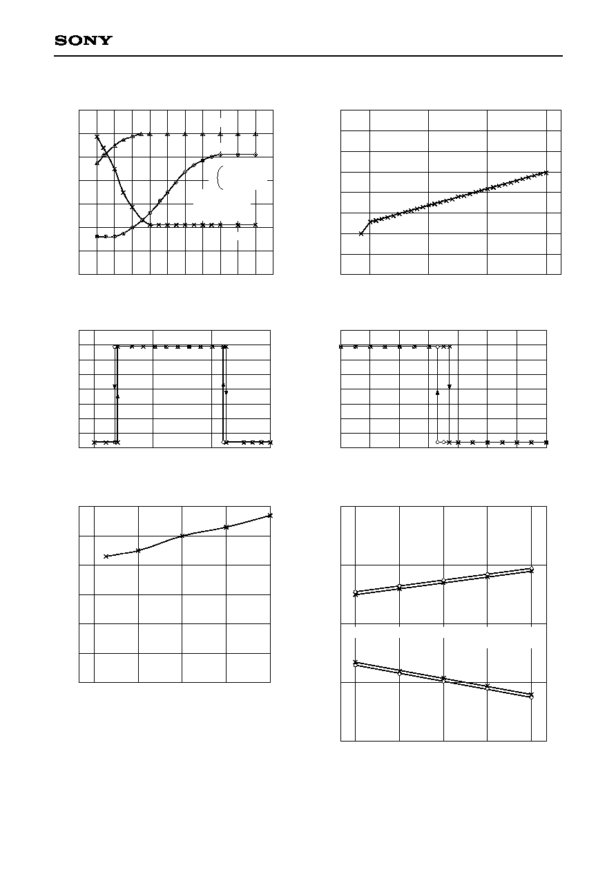
11) S Curve Characteristics
Even if the IF IN input signal frequency is deviated, the feedback is applied to the DET OUT operating
point so as to match it to the comparator reference voltage by the quick charge operation shown in Fig. 8.
Therefore, this feedback must be halted in order to evaluate the S curve characteristics.
To execute the evaluation, measure the average voltage on Pin 8 first and input this voltage to Pin 4 from
the external power supply.
C
C H G
B U F
A M P
C O M P
Reference voltage
Fig. 8
--14--
CXA3099N
≠100 ≠90 ≠80 ≠70 ≠60 ≠50 ≠40 ≠30 ≠20 ≠10
0
10
20
30
40
50
0
1000
800
600
400
200
RSSI
S+N+D
1.0
2.0
3.0
4.0
400
500
600
700
800
900
1000
0
0.2
0.4
0.6
0.8
1.0
1.2
1.4
150
200
250
300
A
u
d
i
o
r
e
s
p
o
n
s
e
[
d
B
]
R
S
S
I
o
u
t
p
u
t
v
o
l
t
a
g
e
[
m
V
]
RF input level [dBm]
Audio response and RSSI output voltage characteristics
C
u
r
r
e
n
t
c
o
n
s
u
m
p
t
i
o
n
[
µ
A
]
Supply voltage [V]
Supply voltage vs. Current consumption
C
o
m
p
a
r
a
t
o
r
o
u
t
p
u
t
v
o
l
t
a
g
e
[
V
]
Comparator input voltage [mV]
Deviation comparator characteristics
0
0.2
0.4
0.6
0.8
1.0
1.2
1.4
160
180
200
220
Comparator input voltage [mV]
NRZ comparator characteristics
240
260
280
10
D
e
t
e
c
t
o
r
o
u
t
p
u
t
l
e
v
e
l
[
m
V
r
m
s
]
Temperature [∞C]
Detector output level temperature characteristics
0
≠25
0
25
50
75
20
30
40
50
60
0
50
Level comparator temperature vs.Threshold level
≠50
≠20
0
25
50
75
T
h
r
e
s
h
o
l
d
l
e
v
e
l
-
2
1
4
[
m
V
]
Temperature [∞C]
C
o
m
p
a
r
a
t
o
r
o
u
t
p
u
t
v
o
l
t
a
g
e
[
V
]
O : H
L
X : L
H
No matching circuit
S/N ratio
IF 455kHz -10dBm
Dev: 4.8kHz
AUDIO: 1.6kHz
0dB = 50mVrms
V
CC
=1.4V
Data filter 2.3kHz
25∞C
Example of Representative Characteristics
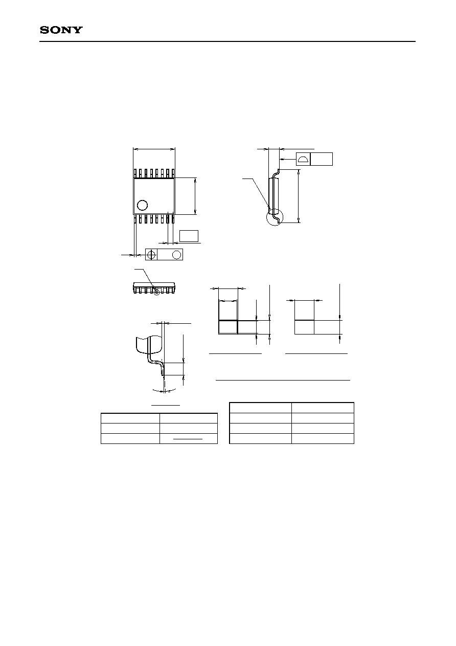
16PIN SSOP (PLASTIC)
SONY CODE
EIAJ CODE
JEDEC CODE
PACKAGE STRUCTURE
PACKAGE MATERIAL
LEAD TREATMENT
LEAD MATERIAL
PACKAGE MASS
EPOXY RESIN
SOLDER / PALLADIUM
42/COPPER ALLOY
0.1g
SSOP-16P-L01
SSOP016-P-0044
b=0.22 ≠ 0.05
+ 0.1
0
.
1
5
≠
0
.
0
2
+
0
.
0
5
PLATING
0.1 ± 0.1
0
.
5
±
0
.
2
0∞ to 10∞
DETAIL A
NOTE: Dimension "
" does not include mold protrusion.
5.0 ± 0.1
0.65
8
1
9
16
4
.
4
±
0
.
1
6
.
4
±
0
.
2
1.25 ≠ 0.1
+ 0.2
A
0.1
0.13 M
B
b
(0.22)
(
0
.
1
5
)
0
.
1
5
≠
0
.
0
1
DETAIL B : SOLDER
DETAIL B : PALLADIUM
+
0
.
0
3
b=0.22 ± 0.03
Package Outline Unit : mm
CXA3099N
--15--
NOTE : PALLADIUM PLATING
This product uses S-PdPPF (Sony Spec.-Palladium Pre-Plated Lead Frame).