 | –≠–ª–µ–∫—Ç—Ä–æ–Ω–Ω—ã–π –∫–æ–º–ø–æ–Ω–µ–Ω—Ç: CXA3108AQ | –°–∫–∞—á–∞—Ç—å:  PDF PDF  ZIP ZIP |

--1--
E99904-TE
Sony reserves the right to change products and specifications without prior notice. This information does not convey any license by
any implication or otherwise under any patents or other right. Application circuits shown, if any, are typical examples illustrating the
operation of the devices. Sony cannot assume responsibility for any problems arising out of the use of these circuits.
Absolute Maximum Ratings (Ta=25 ∞C)
∑ Supply voltage
V
CC
≠0.3 to +5.5
V
∑ Storage temperature
Tstg
≠55 to +150
∞C
∑ Allowable power dissipation
P
D
730
mW
(when mounted on a substrate)
Operating Conditions
∑ Supply voltage
V
CC
4.75 to 5.30
V
∑ Operating temperature
Topr
≠25 to +75
∞C
Description
The CXA3108AQ is a monolithic IC that down-
converts the L-band (1 to 2 GHz) 1st IF to 2nd IF for
satellite broadcast receivers. It integrates a local
oscillator circuit, double-balanced mixer, IF AGC
amplifier and tuning PLL onto a single chip.
This IC supports both analog and digital satellite
broadcasts, and achieves reduction in the number of
tuner components and smaller size.
Features
∑ On-chip tuning PLL
∑ Supports 2.65 GHz oscillator frequency
∑ Noise figure: 12.5 dB typ. (for IF full gain)
∑ IF AGC gain variation: 46 dB typ.
∑ Wide band IF AGC amplifier (60 to 500 MHz)
∑ Two IF outputs
∑ PLL supports I
2
C protocol
∑ On-chip high voltage drive transistor for charge
pump
Applications
∑ Analog satellite broadcast tuners (BS/CS)
∑ Digital satellite broadcast tuners (DSS/DVB, etc.)
Structure
Bipolar silicon monolithic IC
L-band Down Converter IC with On-Chip PLL
40 pin QFP (Plastic)
CXA3108AQ
Notes on Handling
This IC has a weak electrostatic discharge strength. Take care when handling the IC.
--2--
CXA3108AQ
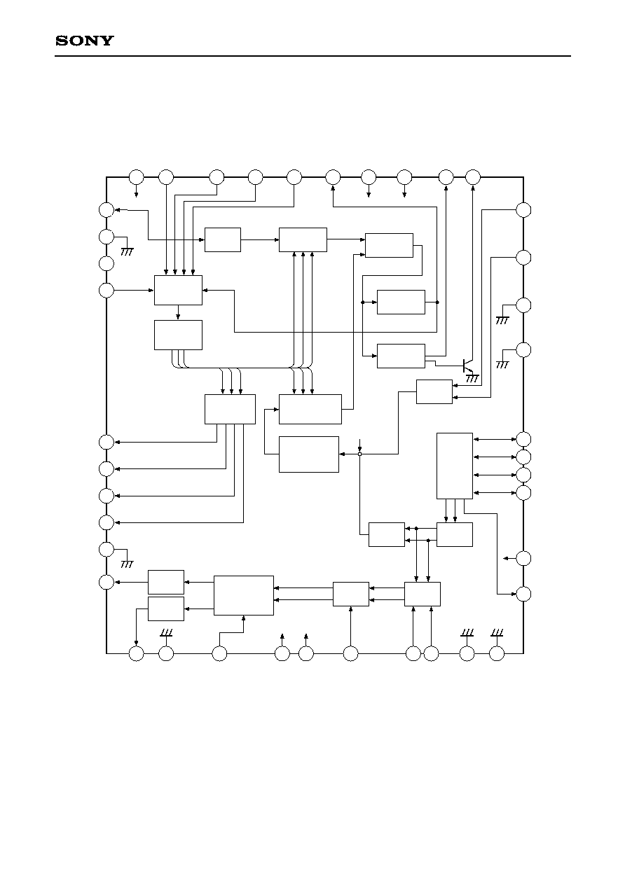
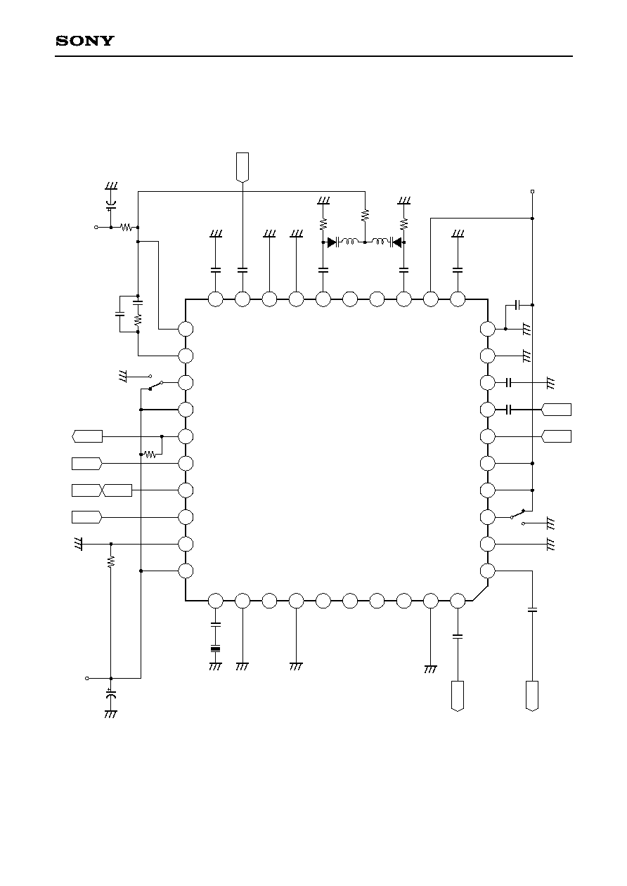
Block Diagram and Pin Configuration
21
36
37
38
40
I
2
C
Receiver
30
29
31
32
35
34
33
Divider
11bit
Phase
Detector
28
27
26
25
22
Shift
Register
39
1
24
23
Lock
Det
Charge
Pump
Buffer
20
19
Divider
17 bit
Prescaler
1/2, 1/1
STSW
Buffer
Buffer
16
15
14
13
OSC
18
17
11
MIX
8
7
10
9
IF AGC
AMP
6
5
4
IF V
CC
SAW
Driver
SAW
Driver
2
OUTPUT SW
3
XTAL
DGND1
NC
BUSSW
PS1
PS2
PS3
PS4
GND
IFOUT2
D
V
C
C
1
A
D
S
W
S
C
L
S
D
A
A
D
C
L
O
C
K
D
V
C
C
2
S
T
S
W
C
P
O
V
T
I
F
O
U
T
1
I
F
G
N
D
2
I
F
S
W
I
F
V
C
C
2
I
F
V
C
C
1
I
F
A
G
C
R
F
I
N
1
R
F
I
N
2
I
F
G
N
D
1
R
F
G
N
D
EXTIN2
EXTIN1
DGND2
GND
OSCB2
OSCE2
OSCE1
OSCB1
RFV
CC
BIAS
REF
OSC
Output Port
Driver
12
--3--
CXA3108AQ
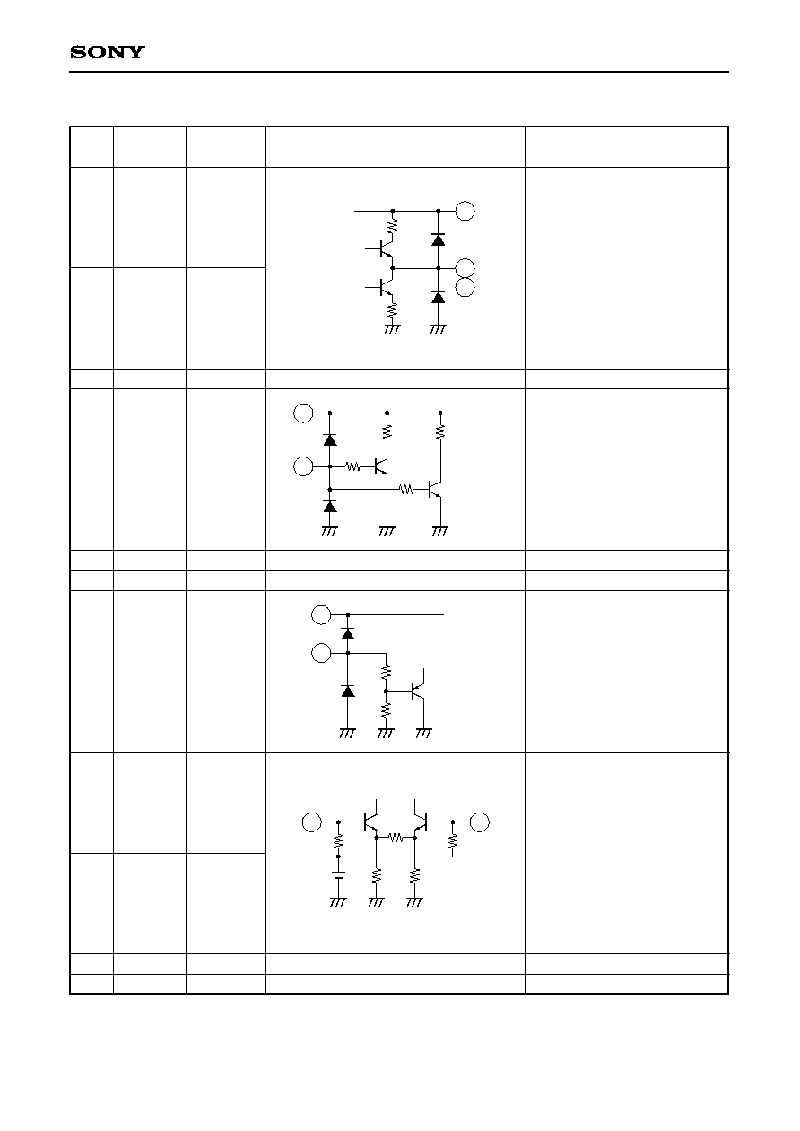
Pin Description
Pin
Symbol
Pin voltage
Equivalent circuit
Description
No.
[V]
1
40
2
3
4
5
6
7
8
9
10
IFOUT1
IFOUT2
IFGND2
IFSW
IFV
CC
2
IFV
CC
1
IFAGC
RFIN1
RFIN2
IFGND1
RFGND
2.5
(IFSW 0 V)
4.7
(IFSW 5 V)
4.7
(IFSW 0 V)
2.5
(IFSW 5 V)
0
0 or 5
5
5
0 to 4
1.7
1.7
0
0
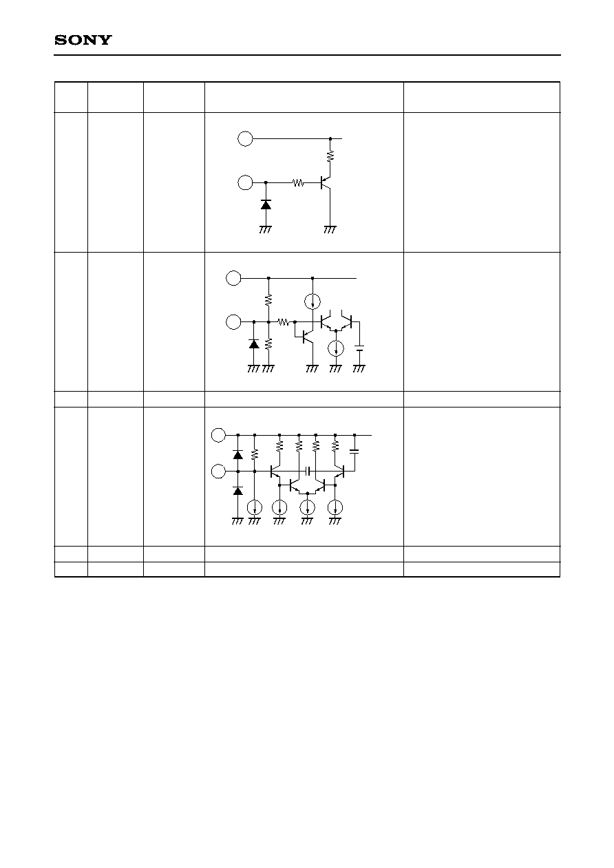
IF outputs.
IF output circuit GND.
Selects whether IF output is
Pin 1 or Pin 40.
When this pin is connected to
GND, the IF signal is output
from Pin 1; when connected to
V
CC
, the IF signal is output from
Pin 40.
IF output circuit power supply.
IF amplifier circuit power supply.
AGC signal input.
RF inputs.
IF amplifier circuit GND.
RF block GND.
IFV
CC
2
4
1
40
IFV
CC
2
4
3
30k
100k
IFV
CC
1
40k
5
40k
6
7
8
2k
2k
--4--
CXA3108AQ
Pin
Symbol
Pin voltage
Equivalent circuit
Description
No.
[V]
11
12
13
14
15
16
17
18
19
20
21
22
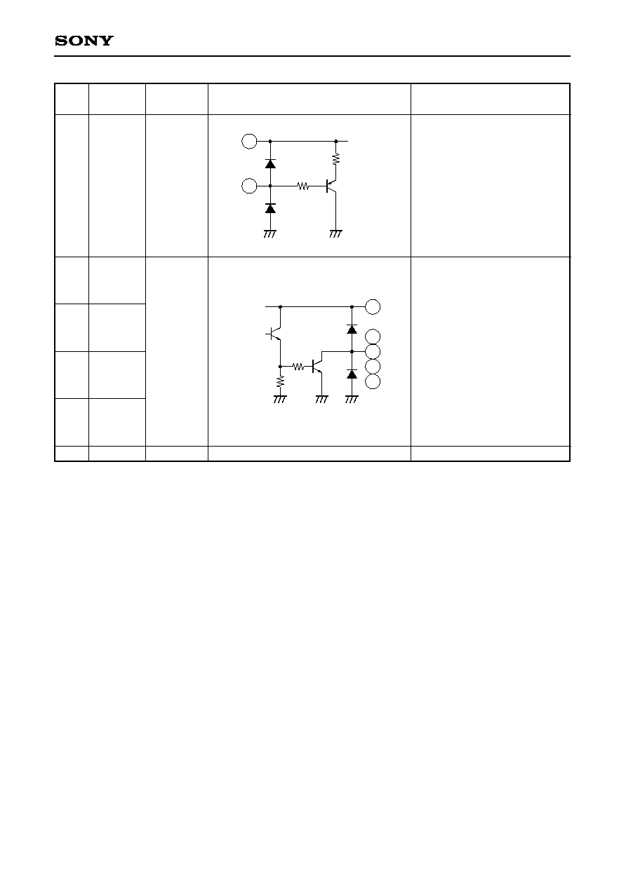
BIAS
RFV
CC
OSCB1
OSCE1
OSCE2
OSCB2
GND
DGND2
EXTIN1
EXTIN2
VT
CPO
1.8
5
2.2
1.5
1.5
2.2
0
0
2.5
2.5
--
--
Oscillator circuit current
adjustment.
Connect this pin to GND via a
capacitor.
RF block power supply.
Oscillator pins.
GND.
Charge pump GND.
PLL external inputs.
NPN transistor output for
varicap diode drive.
Charge pump output.
Connect a loop filter.
RFV
CC
12
11
200
13
2.5k
14
15
16
2.5k
DV
CC
1
30
19
20k
20
25k
25k
5k
5k
DV
CC
2
24
22
200
500
20k
21
--5--
CXA3108AQ
Pin
Symbol
Pin voltage
Equivalent circuit
Description
No.
[V]
23
24
25
26
27
STSW
DV
CC
2
LOCK
ADC
SDA
--
5
5.0
(LOCK)
0.2
(UNLOCK)
--
--
Selects either the internal
oscillator circuit or external input
for input to PLL.
When this pin is open or
connected to V
CC
, the internal
oscillator circuit is selected;
when connected to GND,
external input is selected.
Charge pump power supply.
LOCK detection.
High when locked, Low when
unlocked.
ADC input.
DATA input.
DV
CC
1
20k
30
23
DV
CC
1
30
25
DV
CC
1
30
26
DV
CC
1
30
27
5k
20
2.5k
40k
--6--
CXA3108AQ
Pin
Symbol
Pin voltage
Equivalent circuit
Description
No.
[V]
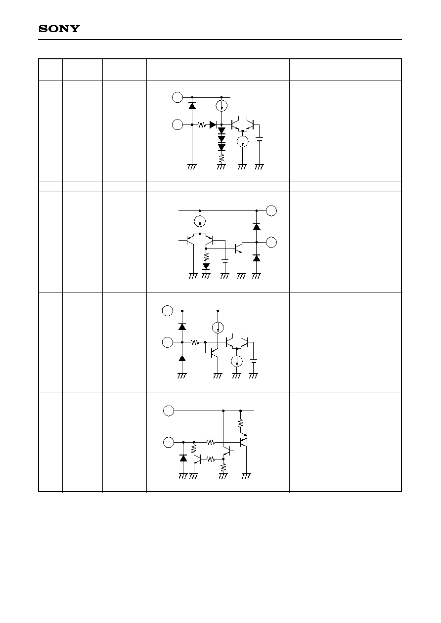
28
29
30
31
32
33
SCL
ADSW
DV
CC
1
XTAL
DGND1
NC
--
1.3
5
4.4
0
--
CLOCK input.
I
2
C bus address selection.
PLL circuit power supply.
Crystal connection for reference
oscillator.
PLL circuit GND.
DV
CC
1
30
28
DV
CC
1
30
29
150k
50k
60k
30p
30p
30
31
DV
CC
1
--7--
CXA3108AQ
Pin
Symbol
Pin voltage
Equivalent circuit
Description
No.
[V]
34
35
36
37
38
39
BUSSW
PS1
PS2
PS3
PS4
GND
--
5.0
(OFF)
0.2
(ON)
0
PLL circuit GND.
Connect directly to GND.
Output ports.
GND.
DV
CC
1
30
34
DV
CC
1
30
36
35
37
38
--8--
CXA3108AQ
Electrical Characteristics
(V
CC
=5 V, Ta=25 ∞C)
Circuit Current
Item
Circuit current A
Circuit current D
Symbol
AI
CC
DI
CC
Measurement conditions
Analog circuit current
Sum of RFV
CC
, IFV
CC
1 and IFV
CC
2 currents
PLL circuit current
Sum of DV
CC
1 and DV
CC
2 currents
Min.
Typ.
Max.
Unit
42
62
82
mA
18
30
40
mA
Item
Conversion gain
Noise figure
IFAGC gain variation
range
IF maximum output
RF pin local oscillator
leak
IF pin local oscillator
leak
Tertiary intermodulation
distortion
Local oscillator phase
noise
RF input impedance
Symbol
CG1
CG2
CG3
NF1
NF2
NF3
AGC
PoSAT
RFLK1
RFLK2
RFLK3
IFLK1
IFLK2
IFLK3
IM3
CN1
CN2
r
C
Measurement conditions
fin=950 MHz, f
IF
=480 MHz
IFAGC=4 V (Full Gain)
fin=1450 MHz, f
IF
=480 MHz
IFAGC=4 V (Full Gain)
fin=2150 MHz, f
IF
=480 MHz
IFAGC=4 V (Full Gain)
fin=950 MHz, f
IF
=480 MHz
IFAGC=4 V (Full Gain)
fin=1450 MHz, f
IF
=480 MHz
IFAGC=4 V (Full Gain)
fin=2150 MHz, f
IF
=480 MHz
IFAGC=4 V (Full Gain)
f
IF
=480 MHz,
50
load saturated output
f
OSC
=1430 to 1830 MHz
f
OSC
=1830 to 2230 MHz
f
OSC
=2230 to 2630 MHz
f
OSC
=1430 to 1830 MHz
f
OSC
=1830 to 2230 MHz
f
OSC
=2230 to 2630 MHz
Pin=≠25 dBm
IFAGC=4 V (Full Gain)
fin=935 MHz, 940 MHz
fout=475 MHz, 480 MHz
S/I of 480 MHz and 475 MHz
f
OSC
=1430 MHz
10 kHz offset
f
OSC
=1430 MHz
100 kHz offset
f=950 MHz
f=950 MHz
Min.
Typ.
Max.
Unit
15
21
25
dB
14
20
24
dB
18
24
28
dB
13
16
dB
13
16
dB
13
16
dB
35
50
dB
9
dBm
≠20
dBm
≠20
dBm
≠25
dBm
≠18
dBm
≠18
dBm
≠20
dBm
38
45
dB
80
dBc/Hz
100
dBc/Hz
12.9
1.84
pF
OSC/MIX/IF Amplifier Blocks
--9--
CXA3108AQ
PLL Block
Item
External local input level
SDA, SCL
High level input voltage
Low level input voltage
High level input current
Low level input current
SDA Low output voltage
Clock input hysteresis
CPO (charge pump)
Output current 1
Output current 2
ADC
Input current
LOCK
High output voltage
Low output voltage
REFOSC
Oscillator frequency range
Input capacitance
Drive level
PS1 to PS4
Pull-in current
Leak current
Symbol
EXT
V
IH
V
IL
I
IH
I
IL
L
SDA
CI
HYS
I
CPO1
I
CPO2
I
ADC
V
LKH
V
LKL
F
XTOSC
C
XTOSC
V
XTOSC
Sink
PS
Leak
PS
Measurement conditions
V
IH
=V
CC
V
IL
=GND
Sink current=3 mA
Byte 4/bit 6=0 and for 3WB
Byte 4/bit 6
Input voltage=5 V
Load resistance 10 k
, for LOCK
Load resistance 10 k
, for UNLOCK
When ON
When OFF
Min.
Typ.
Max.
Unit
≠20
dBm
3
V
CC
V
GND
1.5
V
0
≠0.1
µA
≠1
≠2
µA
0.4
V
0.25
0.4
0.65
V
±35
±50
±75
µA
±125
±180
±270
µA
0.2
µA
V
CC
V
0.5
V
3
12
MHz
14
pF
200
mV
1
mA
200
nA
Bus Timing
Item
I
2
C Bus
SCL clock frequency
Start waiting time
Start hold time
Low hold time
High hold time
Start setup time
Data hold time
Data setup time
Rise time
Fall time
Stop setup time
Symbol
f
SCL
t
WSTA
t
HSTA
t
LOW
t
HIGH
t
SSTA
t
HDAT
t
SDAT
t
R
t
F
t
SSTO
Measurement conditions
Min.
Typ.
Max.
Unit
0
400
kHz
1300
ns
600
ns
1300
ns
600
ns
600
ns
1300
ns
600
ns
300
ns
300
ns
600
ns
--10--
CXA3108AQ
Electrical Characteristics Measurement Circuit
X
T
A
L
D
G
N
D
1
N
C
B
U
S
S
W
P
S
1
P
S
2
P
S
3
P
S
4
G
N
D
I
F
O
U
T
2
E
X
T
I
N
2
E
X
T
I
N
1
D
G
N
D
2
G
N
D
O
S
C
B
2
O
S
C
E
2
O
S
C
E
1
O
S
C
B
1
R
F
V
C
C
B
I
A
S
DV
CC
1
AD
SW
SC
L
SD
A
AD
C
LO
CK
DV
CC
2
ST
SW
CP
O
VT
IF
OU
T1
IF
GN
D1
IF
SW
IF
V
CC
2
IF
V
CC
1
IF
AG
C
RF
IN
1
RF
IN
2
IF
GN
D1
RF
GN
D
1
0
0
p
1
n
SC
L
SD
A
LO
CK
1
0
k
5
V
I
F
o
u
t
2
1
n
I
F
o
u
t
1
IF
AG
C
RF
in
1
0
0
p
1
0
0
p
1
n
1
n
1
5
p
1
k
1
k
E
X
T
I
N
1
T
3
7
9
1
T
3
7
9
1
k
1
5
p
1
n
0
.
1
µ
5
V
1
0
k
1
µ
3
0
V
6
.
2
k
3
3
0
n
6
8
n
C
X
A
3
1
0
8
A
Q
AD
Cin
3
1
3
2
3
3
3
4
3
5
3
6
3
7
3
8
3
9
4
0
1
1
1
2
1
3
1
4
1
5
1
6
1
7
1
8
1
9
2
0
1
2
3
4
5
6
7
8
9
1
0
2
1
2
2
2
3
2
4
2
5
2
6
2
7
2
8
2
9
3
0

--11--
CXA3108AQ
Description of Functions
The CXA3108AQ is a tuner IC for satellite broadcast receivers. It converts the RF signal down-converted to
1st IF (1 to 2 GHz) at the LNB to 2nd IF, so that only the desired reception frequency is selected and
detected.
This IC combines the mixer, local oscillator and IF amplifier (variable gain) circuits required for frequency
conversion to 2nd IF, and the PLL circuit which controls the local oscillator frequency onto a single chip.
The function of each block is described below.
1. Mixer Circuit
This circuit outputs the frequency difference between the signal input to RF IN and the local oscillator
signal. A double-balanced mixer with minimal local oscillator signal leak is used. RF input is equivalent to a
differential amplifier with emitter grounding.
2. Local Oscillator Circuit
A Colpitts oscillator with differential operation is used for the oscillator circuit, so it is stable relative to
supply voltage fluctuation, and undesired radiation is suppressed. This circuit also contains a capacitor
which is part of the resonance circuit, so there is minimal parasitic oscillation and design of external circuits
is easier.
3. IF Amplifier Circuit
This circuit amplifies the mixer IF output, and is comprised of an AGC amplifier stage and low impedance
output stage.
The gain can be varied by the AGC pin voltage (range 0 to 4 V) at the AGC amplifier stage. The maximum
gain is approximately 20 dB (voltage gain between RF IN and IF OUT), and the gain variation width is 30
dB or more.
The output stage has two unbalanced outputs, and can directly connect two SAW filters with different pass
bandwidths. Output pin selection is determined by the IF SW pin voltage.
The IF amplifier circuit is a wide band amplifier circuit, and can be used in the IF frequency range of 60 to
500 MHz.
4. PLL Circuit-1 (normal operation: when the STSW pin is open or connected to V
CC
)
The PLL circuit fixes the local oscillator frequency to the desired frequency. It consists of the prescaler,
main divider, reference divider, phase comparator, charge pump and reference oscillator. The control
format supports the I
2
C bus protocol.
When the power (DV
CC
1) is turned on, the power-on reset circuit activates and the frequency division data
and control data are all initialized to 0. The power-on reset threshold is 3 V at normal temperature (Ta=25
∞C).
5. PLL Circuit-2 (external input PLL operation: when the STSW pin is connected to GND)
When the STSW pin is connected to GND, the PLL enters independent operation mode where the PLL only
is used with the oscillator signal input from the external signal input pin.
--12--
CXA3108AQ
Description of PLL Block
1. Programming
1-1. The main divider frequency division ratio is obtained according to the following formulas.
fosc = fref
◊
(16M + S) or fosc = fref
◊
2
◊
(16M + S) (when PE = 1)
fosc : local oscillator frequency
fref : comparison frequency
2
: prescaler fixed frequency division ratio (when PE = 1)
M
: main divider frequency division ratio
S
: swallow counter frequency division ratio
The variable frequency division ranges of M and S are as follows.
S
M
4095
0
S
15
During PLL independent operation (STSW = GND), the prescaler halving frequency division cannot be
added.
1-2. I
2
C Bus
This IC conforms to the standard I
2
C bus format, and bidirectional bus control is possible consisting of a
write mode in which various data are received and a read mode in which various data are sent.
Write and read modes are recognized according to the setting of the final bit (R/W bit) of the address
byte. Write mode is set when the R/W bit is "0", and read mode is set when the R/W bit is "1".
1-2-1. Address Setting
The responding address can be changed by the ADSW pin voltage to allow more than one PLL in a
system.
<Table 1> Address
MA1
0
0
1
1
MA0
0
1
0
1
ADSW pin voltage
0 to 0.1 V
CC
OPEN
0.4 V
CC
to 0.6 V
CC
0.9 V
CC
to V
CC
--13--
CXA3108AQ
MODE
Address byte
Status byte
bit7
bit6
bit5
bit4
bit3
bit2
bit1
bit0
1
1
0
0
0
MA1
MA0
1
PR
FL
1
1
1
A2
A1
A0
1-2-2. Data format
Write mode is used to receive various data. In this mode, byte 1 contains the address data, bytes 2 and
3 contain the frequency data, and bytes 4 and 5 contain the various control data.
These data are latch transferred in the manner of byte 1, byte 2 + byte 3, byte 4, and byte 5. When the
correct address is received, the data is recognized as frequency data if the first bit of the next byte is
"0", and as control data if this bit is "1".
Also, when data transmission is stopped part-way, the previously programmed data is valid. Therefore,
once the control data has been programmed, 3-byte commands consisting of the address and
frequency data are possible.
Further, even if the I
2
C bus stop conditions are not met, data can be input by sending the start
conditions and the new address.
In read mode, the power-on reset operation status, phase comparator locked/unlocked status and 5-
value A/D converter input pin voltage status are transmitted to the master.
Power-on reset is set to "1" when the supply voltage (DV
CC
1) power supply is cut off.
If DV
CC
1 is 3 V or higher and the status is output in the read mode, this bit is reset to "0".
Write mode: slave receiver
Read mode: slave transmitter
MODE
Address byte
Divider byte 1
Divider byte 2
Control byte 1
Control byte 2
MSB
LSB
bit7
bit6
bit5
bit4
bit3
bit2
bit1
bit0
1
1
0
0
0
MA1
MA0
0
A
0
M10
M9
M8
M7
M6
M5
M4
A
M3
M2
M1
M0
S3
S2
S1
S0
A
1
M12
M11
PE
R3
R2
R1
R0
A
OS
CP
0
0
P4
P3
P2
P1
A
--14--
CXA3108AQ
<Table 3> Reference Divider Frequency Division Ratio
R3
0
0
0
0
0
0
0
0
1
1
1
1
1
1
1
1
R2
0
0
0
0
1
1
1
1
0
0
0
0
1
1
1
1
R1
0
0
1
1
0
0
1
1
0
0
1
1
0
0
1
1
R0
0
1
0
1
0
1
0
1
0
1
0
1
0
1
0
1
Frequency division ratio
2
4
8
16
32
64
128
256
--
5
10
20
40
80
160
320
A2
0
0
0
0
1
A1
0
0
1
1
0
A0
0
1
0
1
0
ADC pin voltage
0 to 0.15V
CC
0.15 V
CC
to 0.3 V
CC
0.3 V
CC
to 0.45 V
CC
0.45 V
CC
to 0.6 V
CC
0.6 V
CC
to V
CC
P1 to P4
:
port control
M0 to M12 :
main divider frequency division ratio setting
S0 to S3
:
swallow counter frequency division ratio setting
OS
:
varicap output OFF (when "1")
CP
:
charge pump current switching
PE
:
prescaler halving frequency division added (when "1")
PR
:
power-on reset
FL
:
lock detection signal
A0 to A2
:
5-value ADC data (ADC pin voltage conversion: Table 2)
R0 to R3
:
reference divider frequency division ratio selection (Table 3)
<Table 2> ADC Conversion Table
--15--
CXA3108AQ
I
2
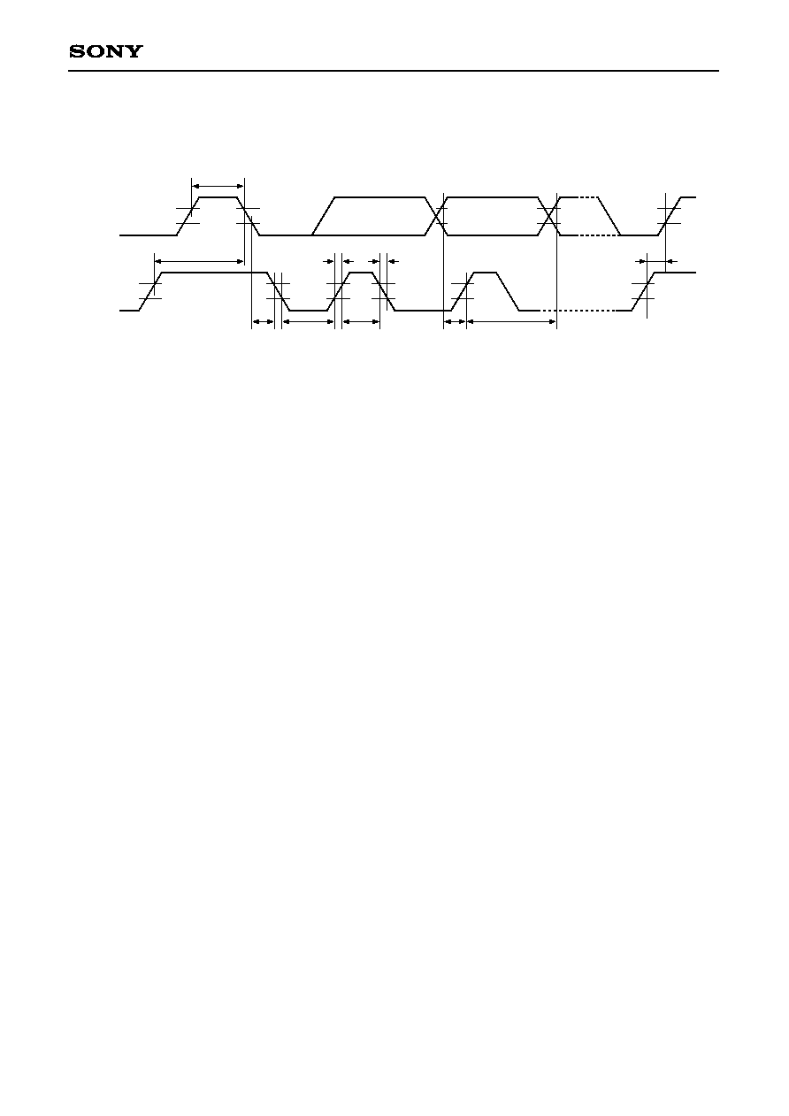
C Bus Timing Chart
t
WSTA
t
SSTA
t
HSTA
t
LOW
t
HIGH
t
R
t
F
t
SDAT
t
HDAT
t
SSTO
START
CLOCK
STOP
t
SSTA
=Start setup time
t
WSTA
=Start waiting time
t
HSTA
=Start hold time
t
LOW
=LOW clock pulse width
t
HIGH
=HIGH clock pulse width
t
SDAT
=Data setup time
t
HDAT
=Data hold time
t
SSTO
=Stop setup time
t
R
=Rise time
t
F
=Fall time
SDA
SCL
DATA CHANGE
--16--
CXA3108AQ
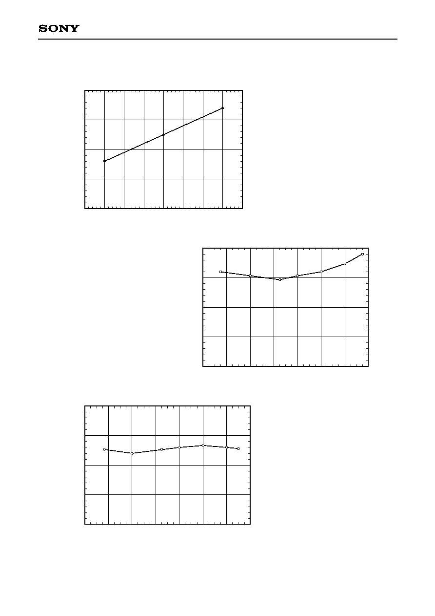
Current consumption characteristics
I
C
C
-
C
u
r
r
e
n
t
c
o
n
s
u
m
p
t
i
o
n
[
m
A
]
V
CC
Supply voltage [V]
100
90
75
4.6
4.7
4.8
4.9
5.1
5.2
5.3
5
95
85
5.4
Conversion gain
IF=480MHz, AGC=4V
C
G
-
C
o
n
v
e
r
s
i
o
n
g
a
i
n
[
d
B
]
RF input frequency [GHz]
25
15
5
0.8
1
1.2
1.4
1.8
2
2.2
1.6
20
10
NF characteristics IF=480 MHz, AGC=4V
Untuned input, DSB display
N
F
-
N
o
i
s
e
f
i
g
u
r
e
[
d
B
]
RF input frequency [GHz]
20
10
0
0.8
1
1.2
1.4
1.8
2
2.2
1.6
15
5
IFOUT
Example of Representative Characteristics
--17--
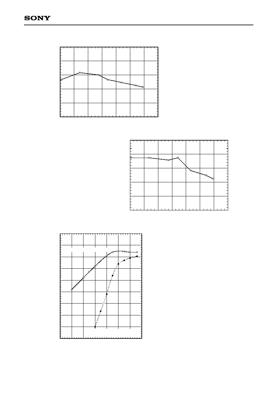
CXA3108AQ
I
F
o
u
t
p
u
t
l
e
v
e
l
[
d
B
m
]
RF input level [dBm] (935MHz, 940MHz)
RF pin local oscillator leak characteristics
R
F
p
i
n
l
o
c
a
l
o
s
c
i
l
l
a
t
o
r
l
e
a
k
[
d
B
m
]
f
OSC
- Local oscillator frequency [GHz]
≠10
≠30
≠60
1.4
1.6
1.8
2
2.4
2.6
2.8
2.2
≠20
≠40
≠50
IFOUT pin local oscillator leak characteristics
AGC=4V
I
F
O
U
T
p
i
n
l
o
c
a
l
o
s
c
i
l
l
a
t
o
r
l
e
a
k
[
d
B
m
]
f
OSC
- Local oscillator frequency [GHz]
≠10
≠30
≠60
1.4
1.6
1.8
2
2.4
2.6
2.8
2.2
≠20
≠40
≠50
20
0
≠60
≠20
≠40
≠60
≠50
≠40
≠30
≠20
≠10
0
10
10
≠10
≠30
≠50
≠70
Fundamental wave (480MHz)
Tertiary intermodulation
distortion component (470MHz)
Input/output characteristics (untuned input, AGC=4V)
--18--
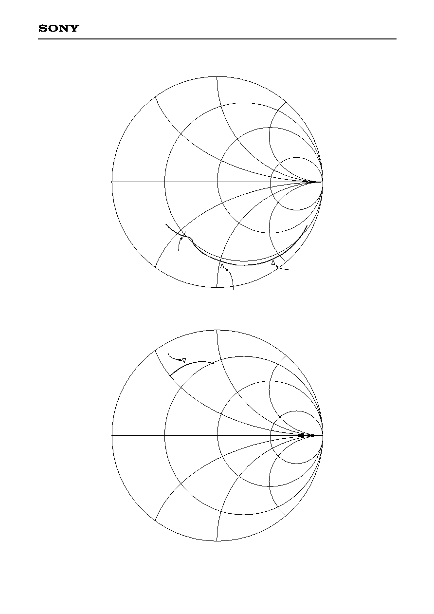
CXA3108AQ
Input Impedance
Output Impedance
950MHz
1
2
1450MHz
3
2150MHz
1
479.5MHz
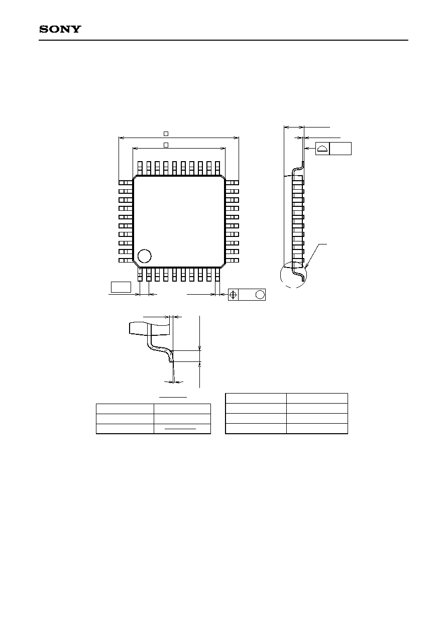
SONY CODE
EIAJ CODE
JEDEC CODE
PACKAGE MATERIAL
LEAD TREATMENT
LEAD MATERIAL
PACKAGE MASS
EPOXY RESIN
SOLDER / PALLADIUM
42/COPPER ALLOY
PACKAGE STRUCTURE
PLATING
0.2g
QFP-40P-L01
QFP040-P-0707
40PIN QFP (PLASTIC)
9.0 ± 0.4
+ 0.4
0.3 ≠ 0.1
1
10
11
20
21
30
31
40
1.5 ≠ 0.15
+ 0.35
0.127 ≠ 0.05
+ 0.1
(
8
.
0
)
A
A
DETAIL
0.1 ≠ 0.1
+ 0.15
+ 0.15
7.0 ≠ 0.1
0
.
5
±
0
.
2
0.1
M
0.24
0.65
0∞ to 10∞
Package Outline Unit : mm
CXA3108AQ
--19--