--1--
E97944-TE
Sony reserves the right to change products and specifications without prior notice. This information does not convey any license by
any implication or otherwise under any patents or other right. Application circuits shown, if any, are typical examples illustrating the
operation of the devices. Sony cannot assume responsibility for any problems arising out of the use of these circuits.
Absolute Maximum Ratings (Ta = 25 ∞C)
∑ Supply voltage
V
CC
1,V
CC
2
≠0.3 to +5.5
V
V
CC
3
≠0.3 to +10.0
V
∑ Storage temperature
Tstg
≠55 to +150
∞C
∑ Allowable power dissipation
P
D
880
mW
(when mounted on a substrate)
Operating Conditions
∑ Supply voltage
V
CC
1, V
CC
2
4.75 to 5.3
V
V
CC
3
4.75 to 9.45
V
∑ Operating temperature
Topr
≠20 to +75
∞C
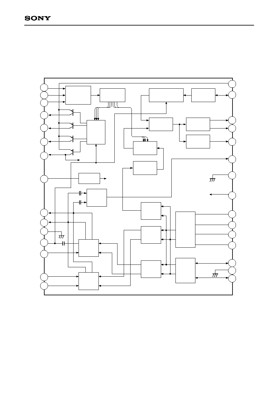
Description
The CXA3185/3186N is a monolithic TV tuner IC
which integrates local oscillator and mixer circuits for
VHF band, local oscillator and mixer circuits for UHF
band, an IF amplifier and a tuning PLL onto a single
chip, enabling further miniaturization of the tuner.
Features
∑ Low noise figure
∑ Low power consumption (5 V, 54 mA typ.)
∑ On-chip tuning PLL (3-wire bus format)
∑ Selection of frequency steps 31.25 kHz, 50 kHz
and 62.5 kHz
∑ On-chip 4-output band switch
Applications
∑ TV tuners
∑ VCR tuners
∑ CATV tuners
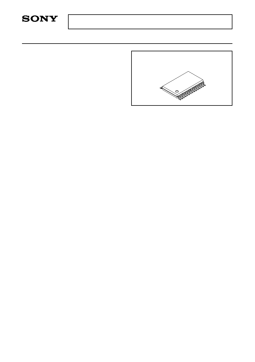
Structure
Bipolar silicon monolithic IC
All Band TV Tuner IC with On-chip PLL
30 pin SSOP (Plastic)
CXA3185/3186N
Note)
Electrostatic discharge strength is weak, and care should be taken in handling this IC.
--3--
CXA3185/3186N
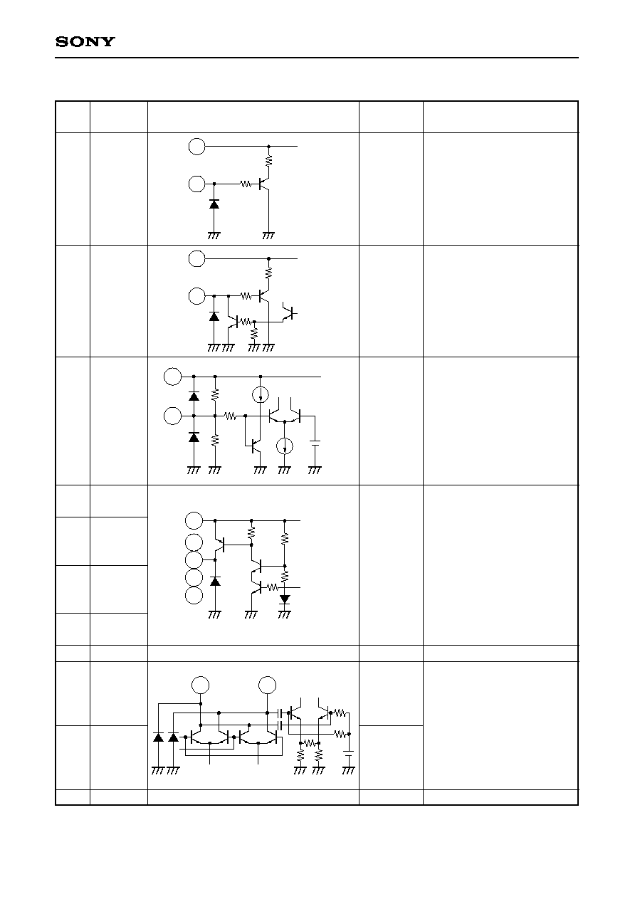
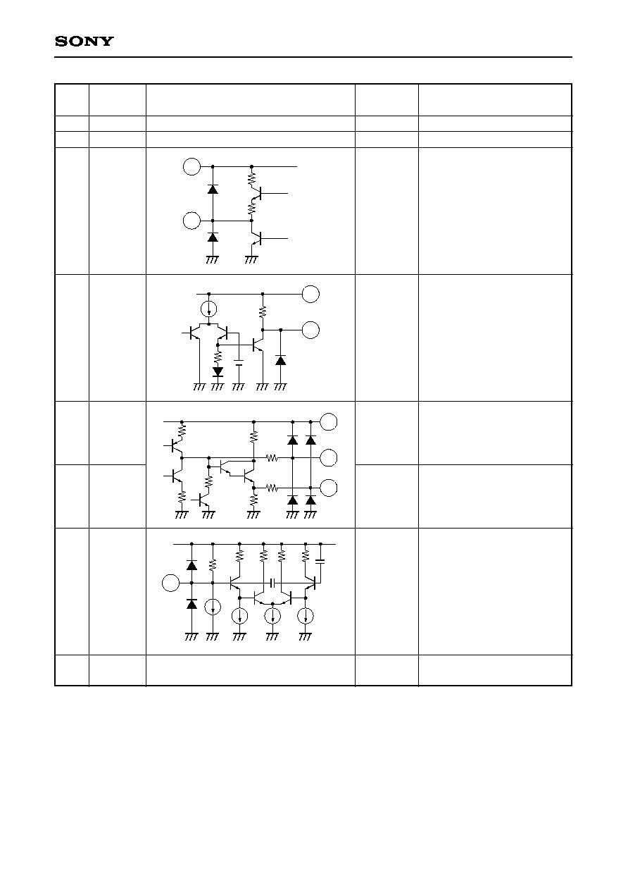
Pin Description
Pin
Symbol
Equivalent circuit
Pin voltage
Description
No.
(V)
1
2
3
4
5
6
7
8
9
10
11
CL
DA
CE
FMT
BVL
BVH
BU
V
CC
1
MIXout1
MIXout2
GND1
--
--
1.25
(when open)
ON : Vcc3
OFF : 0
--
Clock input.
Data input.
Enable pin.
4 : Output for FM TRAP.
5 : Power supply output for
VL band.
6 : Power supply output for
VH band.
7 : Power supply output for
UHF band.
The selected band pin goes
High.
Analog circuit power supply.
Mixer outputs.
Analog circuit GND.
5k
100k
1
22
V
CC
2
5k
100k
2
22
V
CC
2
3
150k
50k
V
CC
2
22
4
5
6
7
30
V
CC
3
20k
9
10
--
--4--
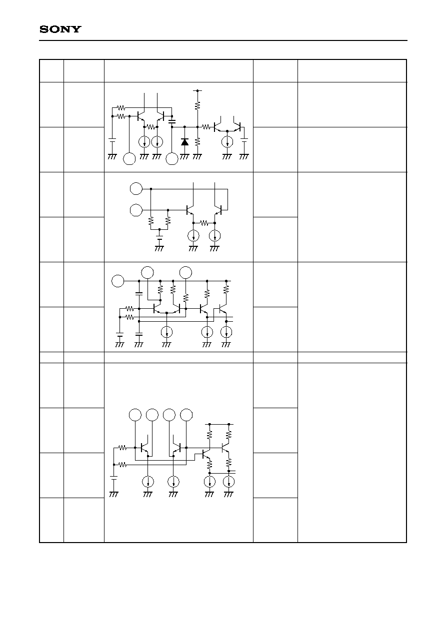
CXA3185/3186N
Pin
Symbol
Equivalent circuit
Pin voltage
Description
No.
(V)
12
13
14
15
16
18
17
19
20
21
22
MS
VHFin
UHFin1
UHFin2
VOSC1
VOSC2
GND
UOSCB1
UOSCE1
UOSCE2
UOSCB2
1.5
(when open)
2.3
(VHF)
0
(UHF)
0
(VHF)
2.3
(UHF)
0
(VHF)
2.3
(UHF)
3.0
(VHF)
3.1
(UHF)
3.5
(VHF)
5.0
(UHF)
--
3.2
(VHF)
2.9
(UHF)
--
(VHF)
2.4
(UHF)
--
(VHF)
2.4
(UHF)
3.2
(VHF)
2.9
(UHF)
Frequency step mode
selection. Five modes can be
selected according to the
applied voltage.
VHF input.
The input format is unbalanced
input.
UHF input.
The input method can be
selected from balanced input
or unbalanced input.
External resonance circuit
connection for VHF oscillator.
GND
External resonance circuit
connection for UHF oscillator.
50k
V
CC
2
120k
12
13
14
15
3k
3k
18
16
8
8p
3k
3k
15p
50
V
CC
1
600
19
22
20
21
3k
3k
V
CC
1
--5--
CXA3185/3186N
Pin
Symbol
Equivalent circuit
Pin voltage
Description
No.
(V)
23
24
25
26
27
28
29
30
V
CC
2
GND2
IFOUT
LOCK
CPE
CPO
REFOSC
V
CC
3
--
--
2.3
5.0
(Lock)
0.2
(UNLock)
0.6
2.0
4.3
--
PLL circuit power supply.
PLL circuit GND.
IF output.
LOCK detection.
High when locked, Low when
unlocked.
NPN transistor connection for
varicap diode drive.
Charge pump output.
Connect a loop filter.
Crystal connection for
reference oscillator.
Power supply for external
supply.
25
8
40
V
CC
1
26
22
V
CC
2
40k
28
27
22
V
CC
2
200
500
20k
29
60k
30p
30p
--
--