 | –≠–ª–µ–∫—Ç—Ä–æ–Ω–Ω—ã–π –∫–æ–º–ø–æ–Ω–µ–Ω—Ç: CXA3304N | –°–∫–∞—á–∞—Ç—å:  PDF PDF  ZIP ZIP |

--1--
E98X40-TE
Sony reserves the right to change products and specifications without prior notice. This information does not convey any license by
any implication or otherwise under any patents or other right. Application circuits shown, if any, are typical examples illustrating the
operation of the devices. Sony cannot assume responsibility for any problems arising out of the use of these circuits.
Absolute Maximum Ratings (Ta=25 ∞C)
∑ Supply voltage
V
CC
14.0
V
∑ Operating temperature
Topr
≠30 to +100
∞C
∑ Storage temperature
Tstg
≠65 to +150
∞C
∑ Allowable power dissipation
P
D
300
mW
Operating Condition
Supply voltage
V
CC
2.5 to 5.5
V
Description
The CXA3304N is an IF signal processing IC for
the ETC car-mounted system which employs the
newest bipolar process.
Features
∑ Low current consumption 7.8 mA
(typ. at V
CC
=3.0 V)
∑ Small package 16-pin SSOP
∑ 40 MHz IF amplifier
∑ RSSI function
∑ RSSI buffer
∑ Peak hold circuit for carrier detection
∑ Comparator for carrier detection
∑ Comparator for data output waveform shaping
∑ Sleep mode supported
Application
ETC car-mounted system
Structure
Bipolar silicon monolithic IC
IF IC for ETC
16 pin SSOP (Plastic)
CXA3304N

--2--
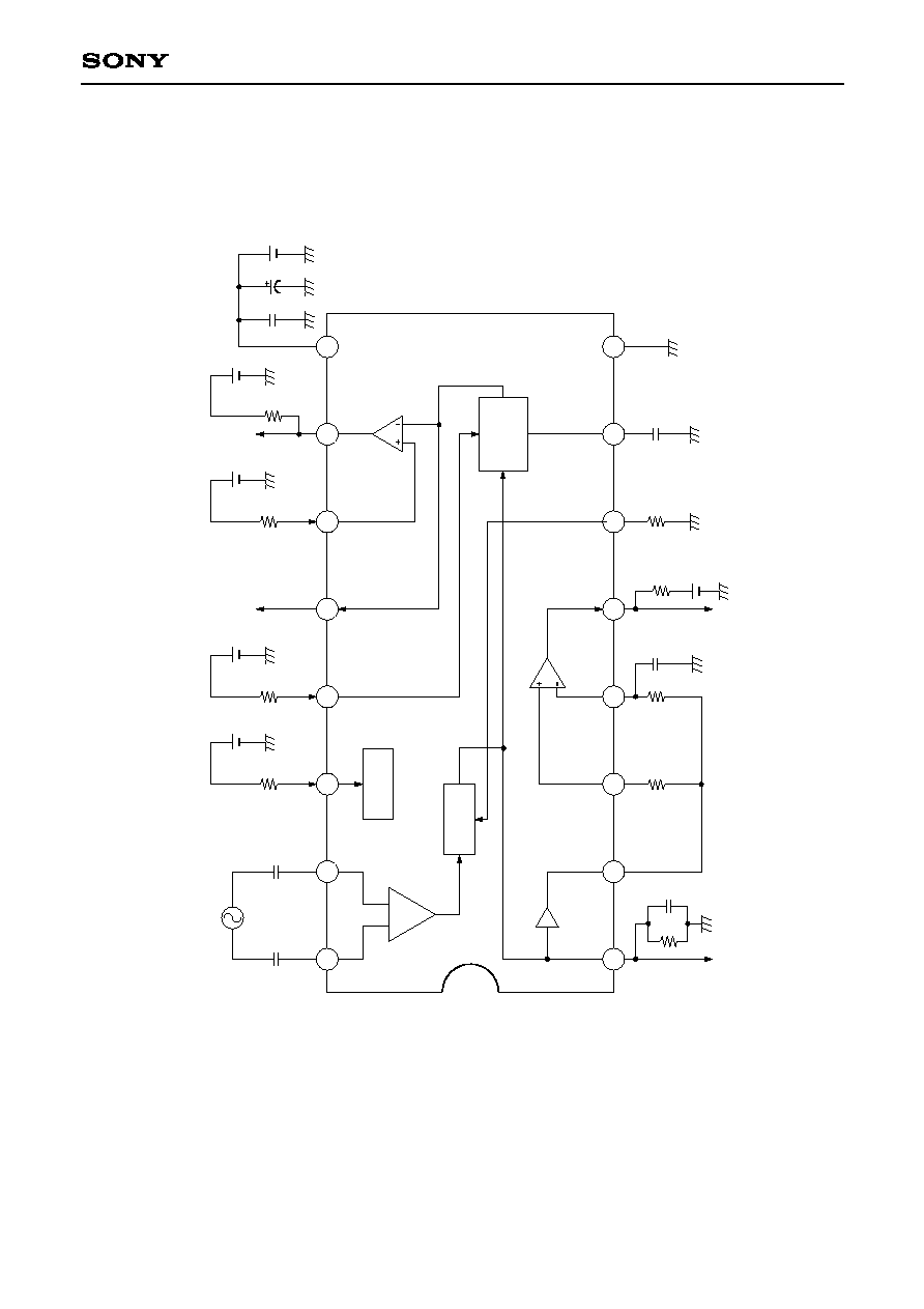
CXA3304N
1
2
3
4
5
6
7
8
9
10
11
12
13
14
15
16
LIM
BIAS
RSSI
COMP1
COMP2
PEAK
HOLD
V
CC
CARRIER SENSE
VREF
RSSI PEAK
PEAK HOLD
POWER SA
VE
XIF IN
IF IN
RSSI OUT
BUFFER OUT
COMP IN
REF IN
DA
T A
OUT
RSSI REF
HOLD CAP
GND
Block Diagram and Pin Configuration

--3--
CXA3304N
Pin
Symbol
Pin
Equivalent circuit
Description
No.
voltage
1
2
3
4
5
10
6
RSSI OUT
BUFFER OUT
COMP IN
REF IN
DATA OUT
CARRIER SENSE
RSSI REF
--
--
--
--
--
0.2 V
RSSI output and RSSI buffer
input.
The current output is converted
to the voltage and it undergoes
the waveform shaping by the
external resistor and capacitor.
The input/output voltage range
is between 0.2 V to 1.4 V.
Buffer output which outputs the
RSSI voltage.
Comparator input.
Comparator reference voltage
input.
Comparator output.
Open collector.
Connects the resistor which
determines the output current
characteristics for the RSSI
circuit.
GND
10
5
V
CC
62
V
CC
GND
6
124
124
GND
3
4
V
CC
124
124
1
2
V
CC
GND
124
124
Pin Description

--4--
CXA3304N
Pin
Symbol
Pin
Equivalent circuit
Description
No.
voltage
7
8
9
11
12
13
14
15
16
HOLD CAP
GND
V
CC
VREF
RSSI PEAK
PEAK HOLD
POWER SAVE
XIF IN
IF IN
--
--
--
--
--
--
--
0 V
Connects the external capacitor
which determines the peak hold
time constant.
The bias current of the internal
buffer circuit flows even in hold
mode.
Ground.
V
CC
.
Input of voltage which is the
threshold value of the carrier
sense comparator.
RSSI peak voltage output.
This is also connected to the
input pin for the carrier sense
comparator.
Peak hold circuit control.
Peak hold for low;
reset operation for high.
Power saving control.
Sleep mode for low;
IC operation for high.
IF signal input.
It is input with DC coupled.
Input the IF signal via a
matching circuit.
GND
7
V
CC
124
V
CC
GND
11
12
124
124
GND
V
CC
13
14
20k
(28k)
80k
(120k)
V
CC
GND
15
16
1.5k
1.5k

--5--
CXA3304N
Item
Current consumption
Current consumption
Logic input voltage
high level
Logic input voltage
low level
IF limiter
input resistance
Comparator 1
output saturation voltage
Comparator 1
output leak current
Comparator 1
output current
Comparator 2
output saturation voltage
Comparator 2
output leak current
Comparator 2
output current
RSSI output voltage 1
RSSI output voltage 2
RSSI output voltage 3
RSSI
buffer output current +
RSSI
buffer output current ≠
Peak hold
leak current
Peak hold
charge current
Peak hold
discharge current
Pin 11 input current
Pin 13 input current
Pin 14 input current
Symbol
I
CC
I
CCS
Vth
Vtl
Rif
Vst1
Icl1
Io1
Vst2
Icl2
Io2
Vr1
Vr2
Vr3
Irs +
Irs ≠
Ipl
Ipc
Ipd
I11
I13
I14
Condition
Vin=0 V, Pin 9 current
V14=0 V, Pin 9 current
--
--
DC voltage
I5=640 µA, V3=0.16 V, V4=0.2 V
V5=3 V, V3=0.24 V, V4=0.2 V
V5=0.4 V, V3=0.16 V, V4=0.2 V
I10=300 µA, V11=0.2 V, V7=0.24 V
V10=3 V, V11=0.2 V, V7=0.16 V
V10=0.4 V, V11=0.2 V, V7=0.24 V
Vin=≠67 dBm, 40 MHz
Vin=≠47 dBm, 40 MHz
Vin=≠17 dBm, 40 MHz
V1=1.4 V, V2=0.2 V
V1=0 V, V2=1.4 V
V13=0 V, V1=0.2 V, V7=1.4 V
Pin 7 current
V13=0 V, V7=0.2 V, V1=1.4 V
Pin 7 current
V7=1.4 V
Pin 7 current
V11=0, V7=1.4 V
--
V14= 1 V
Min.
Typ.
Max.
Unit
5.5
7.8
10
mA
--
33
100
µA
1
--
V
CC
V
0
--
0.35
V
1.2
1.5
1.8
k
--
0.15
0.4
V
--
0
5
µA
640
--
--
µA
--
0.1
0.4
V
--
0
5
µA
300
--
--
µA
0.2
0.35
0.5
V
0.61
0.81
1.01
V
1.1
1.35
1.655
V
100
--
--
µA
100
130
--
µA
--
0.05
5
µA
100
220
--
µA
100
180
--
µA
--
0.5
50
µA
--
17
50
µA
--
11
50
µA
Electrical Characteristics
(V
CC
=3 V, Ta=25 ∞C)
Unless otherwise specified, V14=3 V, V13=3 V and V11=3 V.
Pin condition Example) V13 : Pin 13 voltage, I5 : Pin 5 current
The external constant is the value shown in the Application Circuit.
--6--
CXA3304N
Electrical Characteristics Measurement Circuit
1
2
3
4
5
6
7
8
9
10
11
12
13
14
15
16
LIM
BIAS
RSSI
COMP1
COMP2
PEAK
HOLD
V
CC
10
µ
10k
V
CC
0.01
µ
CARRIER SENSE
V11
RSSI PEAK
Vhold
Vsave
Vin
1000p
1000p
RSSI OUT
5p
100p
22k
22k
2.2k
DATA OUT
1k
4.7k
V
CC
470p

--7--
CXA3304N
Application circuits shown are typical examples illustrating the operation of the devices. Sony cannot assume responsibility for
any problems arising out of the use of these circuits or for any infringement of third party patent and other right due to same.
1
2
3
4
5
6
7
8
9
10
11
12
13
14
15
16
1
PO
WER SA
VE
PEAK HOLD
RSSI PEAK
VREF
CARRIER SENSE
V
CC
I
CC
I
CC
V
CC
IF IN
XIF IN
RESET
SLEEP
PEAK
HOLD
A
CTIVE
OPEN
BIAS
OPEN
V
CC
R8
10
GND
GND
GND
GND
GND
GND
HOLD CAP
RSSI REF
V
CC
OPEN
B
UFFER OUT
RSSI OUT
C1
L1
820nH
1000p
C3
1000p
C4
0.01
µ
C5
0.01
µ
C14
0.01
µ
C13
10
µ
S2
R7
10k
C11
10
µ
R9
10
C12
0.01
µ
C9
S4
S5
S6
S3
R6
0.01
µ
C10
470p
R5
S1
1k
C8
0.01
µ
C7
10
µ
R4
4.7k
C6
100p
R3
22k
R2
22k
C2
5p
R1
2.2k
D
A
T
A
OUT
IF_IN
(50
)
CXA3304N
100k
4.5 to 20pF
C15
Application Circuit

--8--
CXA3304N
Description of Operation
1) Power supply
This IC has a built-in regulator and is designed for stable operation over a wide range of supply voltages
from 2.5 to 5.5 V. Wiring to the power supply pin should be decoupled as close to the pin as possible. In
addition, the Pin 9 power supply line and the power supply line connected to the comparator output pull-up
resistor should be separated as necessary. The IC can also be set to sleep mode to reduce power
consumption by controlling Pin 14.
2) Limiter amplifier
This is a differential input type limiter amplifier. The input impedance is approximately 700
. Input the IF
signal via a matching circuit.
3) RSSI circuit
This circuit outputs a current corresponding to the amplitude of the IF signal input to the limiter amplifier. If
the IF signal is the ASK signal, demodulated output is obtained. Connect a resistor to Pin 1 to convert the
voltage. Adjusting this resistance value also changes the RSSI output voltage, but the value should be set
so that the output voltage is smaller than the supply voltage ≠1.1 V. The output current includes a
component twice the IF signal frequency. Adjust the value of the Pin 1 external capacitor as necessary.
Connect a resistor to Pin 6 for determining the temperature characteristics of the RSSI circuit output
current.
Pin 2 is the RSSI circuit buffer output. The output range is from approximately 0.2 V to the supply voltage -
1.1 V.
4) COMP1 circuit
This is the comparator circuit for shaping the ASK demodulation signal waveform. The output is an open
collector. Connect this circuit to the power supply, etc., via a pull-up resistor. Set the connected power
supply to the Pin 9 potential or lower.
Pin 14 voltage
Function
HI
IC operation mode
LOW
Sleep mode

--9--
CXA3304N
5) Peak hold circuit
This circuit holds the Pin 1 RSSI output voltage peak. Peak hold operation and reset operation are
switched with Pin 13.
Peak hold operation
The input RSSI voltage is held by the Pin 7 capacitor. The held voltage passes through the buffer circuit
and is output to Pin 12. The response characteristics during peak hold operation are determined by the
peak hold charge and leak currents, which are determined inside the IC, and the Pin 7 capacitance value.
The held voltage fluctuates according to the peak hold leak current. This fluctuation becomes larger as the
capacitor value is set smaller. Adjust the reset operation interval and the capacitor value as necessary. In
addition, the hold time can also be shortened by connecting a resistor between Pin 7 and GND.
Reset operation
The charge held by the Pin 7 capacitor is discharged according to the peak hold discharge current which is
determined inside the IC. The discharge time changes according to the capacitor value.
6) COMP2 circuit
This is the carrier sense comparator circuit. The input pin is connected internally to the RSSI PEAK output
(Pin 12). Apply the voltage to be used as the threshold value to Pin 11. The comparator output is an open
collector output, and should be connected to the power supply, etc., via a pull-up resistor. Set the
connected power supply to the Pin 9 potential or lower.
Pin 13 voltage
Function
HI
Reset
LOW
Peak hold
--10--
CXA3304N
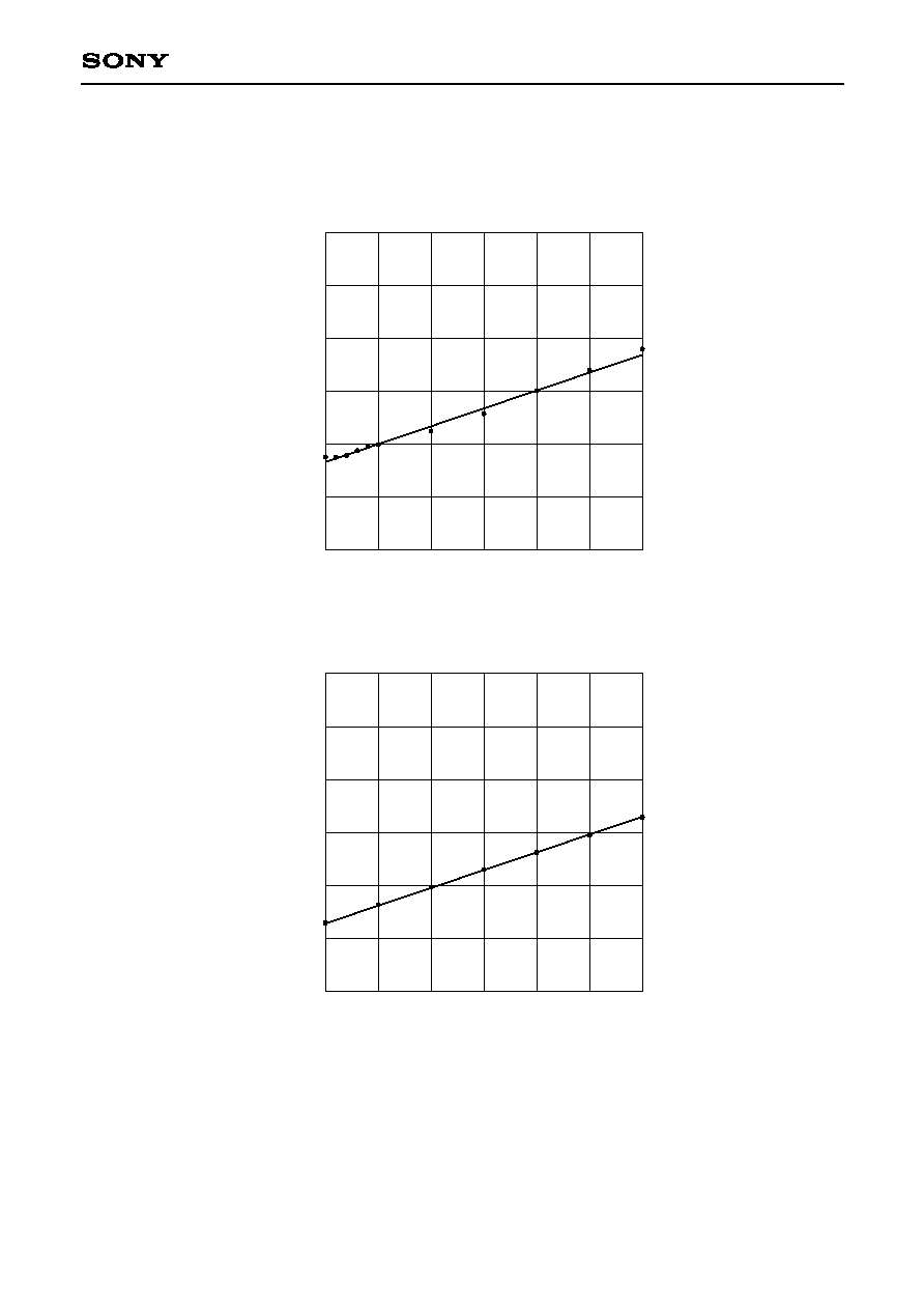
Example Representative Characteristics
Active mode current consumption (P9)
Supply voltage [V]
Activ
e mode current consumption (P9) [mA]
8.1
8.0
7.9
7.8
7.7
7.6
2.5
3.0
3.5
4.0
4.5
5.0
5.5
V
CC
(P9)=3V, P
OW
_SAVE (P14)=1V
Power saving mode current consumption (P9)
Supply voltage [V]
P
o
w
er sa
ving mode current consumption (P9) [
µ
A]
80
60
40
20
0
2.5
3.0
3.5
4.0
4.5
5.0
5.5
V
CC
(P9)=3V, P
OW
_SAVE (P14)=0.35V

--11--
CXA3304N
RSSI output characteristics
IF input power [dBm]
RSSI_OUT (P1) v
oltage [V]
1.4
1.6
1.2
1.0
0.8
0.6
0.4
0.2
0
≠80
≠70
≠60
≠50
≠40
≠30
≠20
≠10
0
10
V
CC
(P9)=3V, IF=40MHz CW
RSSI output temperature characteristics
IF input power [dBm]
RSSI_OUT (P1) v
oltage [V]
1.4
1.6
1.2
1.0
0.8
0.6
0.4
0.2
0
≠80
≠70
≠60
≠50
≠40
≠30
≠20
≠10
0
V
CC
(P9)=3V, IF=40MHz CW
: ≠30
∞
C
: 25
∞
C
: 100
∞
C

Package Outline Unit : mm
CXA3304N
--12--
16PIN SSOP (PLASTIC)
SONY CODE
EIAJ CODE
JEDEC CODE
PACKAGE STRUCTURE
PACKAGE MATERIAL
LEAD TREATMENT
LEAD MATERIAL
PACKAGE MASS
EPOXY RESIN
SOLDER / PALLADIUM
42/COPPER ALLOY
0.1g
SSOP-16P-L01
SSOP016-P-0044
5.0 ± 0.1
0.65
0.22 ≠ 0.05
+ 0.1
8
1
9
16
4.4 ±
0.1
6.4 ±
0.2
0.1 ± 0.1
0.5 ±
0.2
0∞ to 10∞
0.15 ≠ 0.02
+ 0.05
1.25 ≠ 0.1
+ 0.2
A
DETAIL A
0.1
PLATING
NOTE: Dimension "
" does not include mold protrusion.
0.13 M
NOTE : PALLADIUM PLATING
This product uses S-PdPPF (Sony Spec.-Palladium Pre-Plated Lead Frame).