
- 1 -
E06702-CR
Sony reserves the right to change products and specifications without prior notice. This information does not convey any license
by any implication or otherwise under any patents or other right. Application circuits shown, if any, are typical examples illustrating
the operation of the devices. Sony cannot assume responsibility for any problems arising out of the use of these circuits.
CXA3355AER
GPS Down Converter IC
Description
The CXA3355AER is an IC developed as a GPS RF down converter. This IC realizes a reduction in the number
of external parts by integrating an LNA, image rejection mixer, IF filter, PLL and VCO (L, C) into a small
package with low current consumption.
(Applications: GPS down converter IC)
Features
Includes all functions required for the GPS down converter
Low voltage operation: V
CC
= 1.6 to 2.0V
Low current consumption (active mode): 11mA (Typ. at V
CC
= 1.8V, IF
1MHz)
Low current consumption (power save mode) < 1
A
Total gain
100dB
Total NF
4dB
On-chip VCO and PLL
Supports typical TCXO frequencies (13MHz, 16.368MHz, 18.414MHz, etc.)
On-chip LNA (LNA NF: 2.0dB)
Image rejection mixer
On-chip IF filter, and an external filter can be connected as an option for further band narrowing.
1-bit IF output
Antenna sense function
Structure
SiGe BiCMOS monolithic IC
Package
44 pin VQFN (Plastic)

CXA3355AER
- 2 -
Absolute Maximum Ratings
(Ta = 25
∞
C)
Recommended Operating Conditions
Supply voltage
V
CC
1
V
CC
2
V
CC
3
≠0.2 to +2.5
≠0.2 to +3.6
≠0.2 to +3.6
V
V
V
Operating temperature
Topr
≠40 to +85
∞
C
Storage temperature
Tstg
≠65 to +150
∞
C
Supply voltage
V
CC
1
V
CC
2
V
CC
3
1.6 to 2.0
1.6 to 3.3
2.7 to 3.3
V
V
V
CXA3355AER
- 3 -
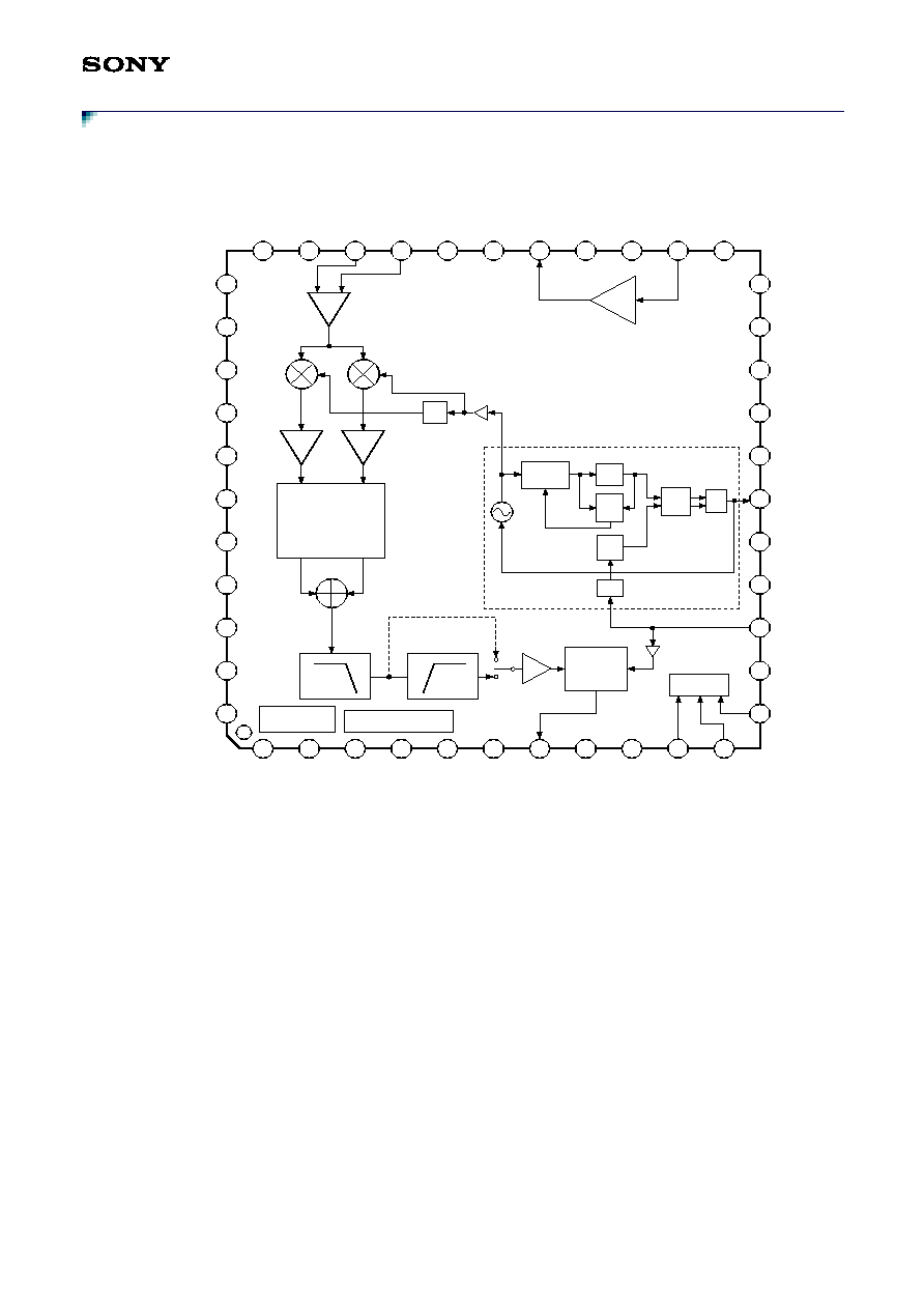
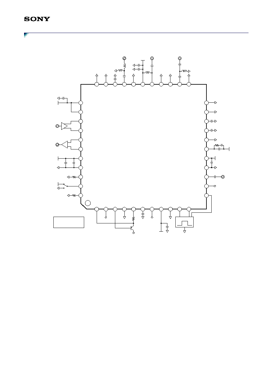
Block Diagram and Pin Configuration
16
17
14
13
15
18
19
20
21
22
23
24
44
43
42
41
40
39
38
37
27
28
29
30
25
26
31
32
33
34
35
36
10
9
8
7
12
11
6
5
4
3
2
1
1540fo = 1575.42MHz
ANT SENSE
RF_AMP
IF_AMP1
IF_AMP1
Mixer
Mixer
LPF
HPF
BIAS
LNA
1536fo [1539fo]
4fo [fo]
DMPS
MC
PFD
RC
CP
SC
PLL
CTL
IF Phase Shifter
A/D
Converter
IF_AMP2
90∞
◊2
GND (RF)
GND (RF)
RF_INP
RF_INN
GND
V
CC
1 (LNA)
LNA_OUT
GND
GND
LNA_IN
GND (LNA)
GND (LNA)
GND (LNA)
VCO_I
C_VCO
GND
LPF
V
CC
1 (PLL)
GND (PLL)
TCXO
CLK_OUT
LT
V
CC
1 (RF)
V
CC
1 (RF)
TESTINP
TESTINN
TESTOUTP
TESTOUTN
V
CC
1 (IF)
GND (IF)
R_EXT1
ENABLE
R_EXT2
ASENS
DIAG
AILIM
GND (ANT)
V
CC
3 (ANT)
C_EXT
DATA_OUT
V
CC
2 (IF)
GND (IF)
DATA
CLK
fo mode: IF = 1.023MHz
4fo mode: IF = 4.092MHz
CXA3355AER
- 4 -
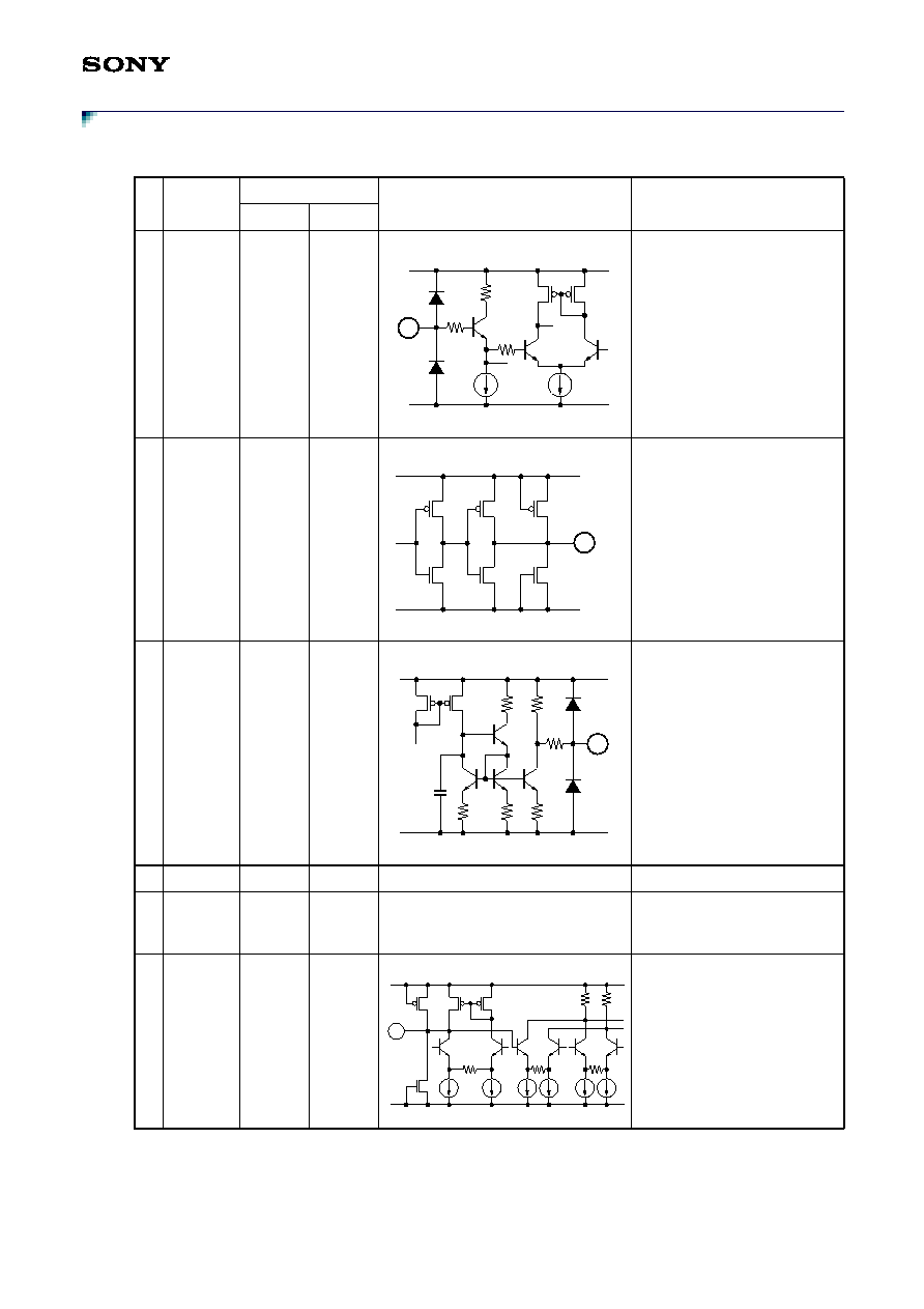
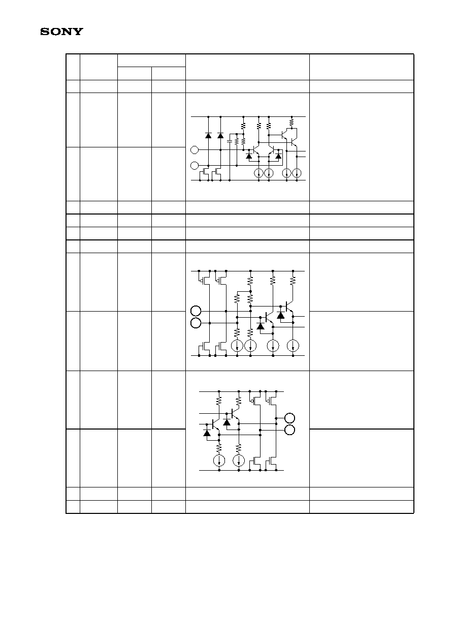
Pin Description
Pin
No.
Symbol
Standard pin voltage [V]
Equivalent circuit
Description
DC
AC
1 ASENS
--
--
Antenna sense input.
2 DIAG
--
--
Antenna sense output.
3 AILIM
--
--
Antenna sense current
limitation.
Connect to the external PNP
transistor base pin.
4 GND (ANT)
0
--
Antenna sense GND.
5 V
CC
3 (ANT)
3.0
--
Antenna sense V
CC
.
Leave open when not using the
antenna sense function.
6 C_EXT
1.2
--
Capacitor connection for
canceling the offset.
V
CC
3 (ANT)
GND (ANT)
1
2
V
CC
3 (ANT)
GND (ANT)
V
CC
3 (ANT)
GND (ANT)
3
6
V
CC
1 (IF)
GND (IF)
CXA3355AER
- 5 -
7 DATA_OUT
--
1.8Vp-p
Data (IF) output.
8 V
CC
2 (IF)
1.8
--
IF block V
CC
.
9 GND (IF)
0
--
IF block GND.
10 DATA
--
--
Serial data input.
11 CLK
--
--
Serial data clock input.
12 LT
--
--
Latch signal input.
13 CLK_OUT
--
1.8Vp-p
TCXO clock output.
Leave open when not using the
TCXO clock.
14 TCXO
--
--
Reference frequency input.
15 GND (PLL)
0
--
PLL block GND.
16 V
CC
1 (PLL)
1.8
--
PLL block V
CC
.
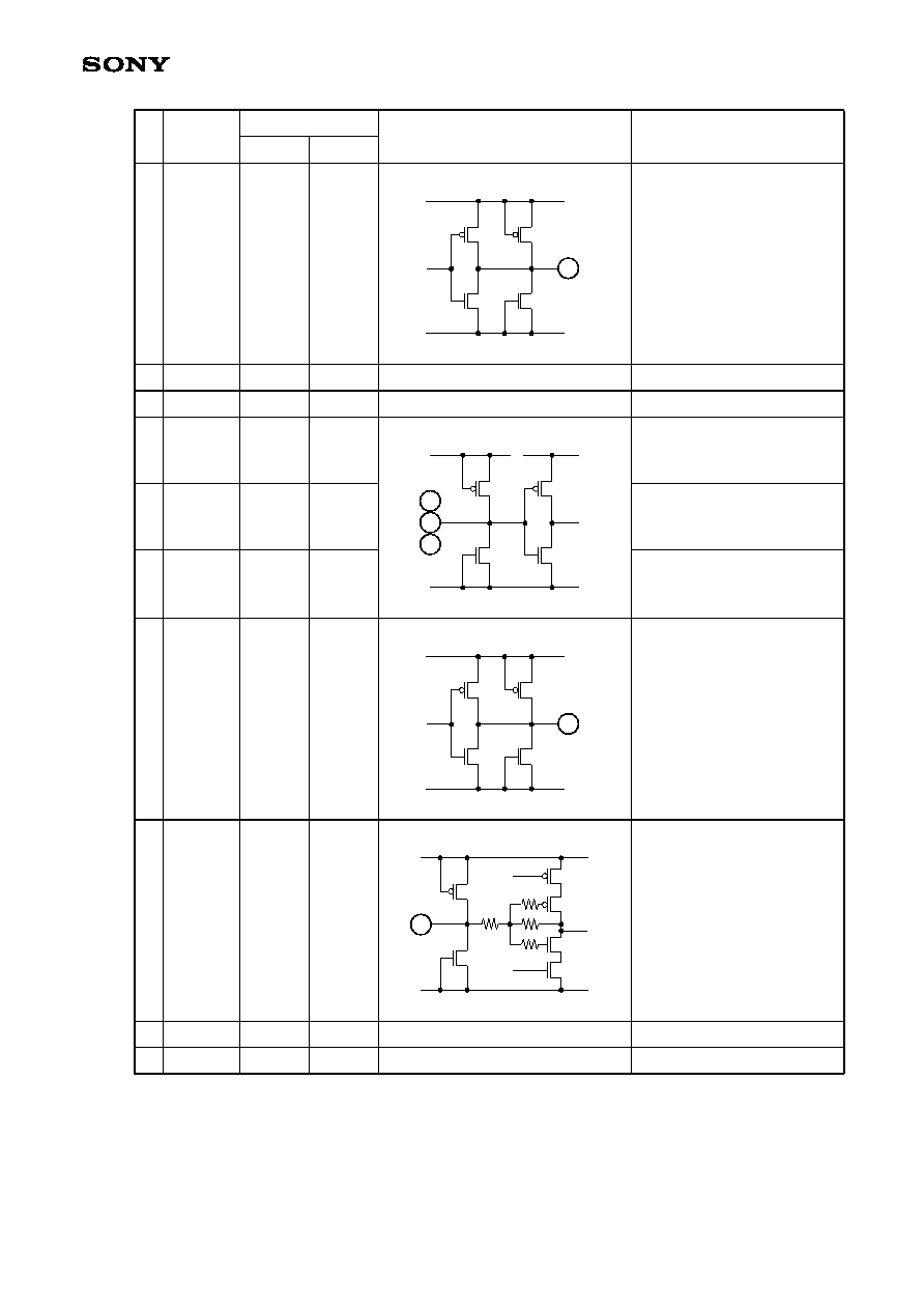
Pin
No.
Symbol
Standard pin voltage [V]
Equivalent circuit
Description
DC
AC
7
V
CC
2 (IF)
GND (IF)
11
10
12
V
CC
1 (PLL)
V
CC
2 (IF)
GND (PLL)
13
V
CC
2 (IF)
GND (IF)
14
V
CC
1 (PLL)
GND (PLL)
CXA3355AER
- 6 -
17 LPF
1.2
--
PLL loop filter connection.
18 GND
0
--
GND.
19 C_VCO
1.1
--
Capacitor connection for
decoupling the VCO bias circuit.
20 VCO_I
0.1
--
Capacitor connection for
decoupling the VCO bias circuit.
21 GND (LNA)
0
--
LNA block GND.
22 GND (LNA)
0
--
LNA block GND.
23 GND (LNA)
0
--
LNA block GND.
24 LNA_IN
0.8
--
LNA input.
27 LNA_OUT
1.8
--
LNA output.
25 GND
0
--
GND.
26 GND
0
--
GND.
28 V
CC
1 (LNA)
1.8
--
LNA block V
CC
.
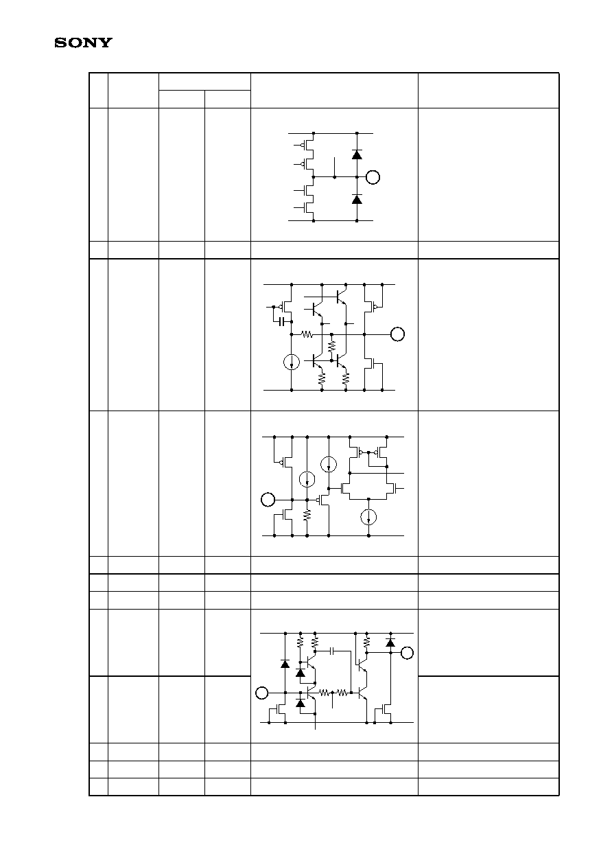
Pin
No.
Symbol
Standard pin voltage [V]
Equivalent circuit
Description
DC
AC
17
V
CC
1 (PLL)
GND (PLL)
19
V
CC
1 (RF)
GND (RF)
20
V
CC
1 (RF)
GND (RF)
V
CC
1 (LNA)
GND (LNA)
24
27
CXA3355AER
- 7 -
29 GND
0
--
GND.
30 RF_INN
1.7
--
RF amplifier input.
31 RF_INP
1.7
--
32 GND (RF)
0
--
RF block GND.
33 GND (RF)
0
--
RF block GND.
34 V
CC
1 (RF)
1.8
--
RF block V
CC
.
35 V
CC
1 (RF)
1.8
--
RF block V
CC
.
36 TESTINP
1.3
--
IF signal input when using an
external filter.
37 TESTINN
1.3
--
IF signal input when using an
external filter.
38 TESTOUTP
0.5
--
IF signal output when using an
external filter.
39 TESTOUTN
0.5
--
IF signal output when using an
external filter.
40 V
CC
1 (IF)
1.8
--
IF block V
CC
.
41 GND (IF)
0
--
IF block GND.
Pin
No.
Symbol
Standard pin voltage [V]
Equivalent circuit
Description
DC
AC
V
CC
1 (RF)
GND (RF)
30
31
37
V
CC
1 (IF)
GND (IF)
36
39
V
CC
1 (IF)
GND (IF)
38

CXA3355AER
- 8 -
42 R_EXT1
0.5
--
External resistor connection.
(bias)
43 ENABLE
--
--
ENABLE signal input.
High (V_IH: 1.2V min.):
Active mode
Low (V_IL: 0.2V max.):
Power save mode
44 R_EXT2
1.2
--
External resistor connection.
(bias)
Pin
No.
Symbol
Standard pin voltage [V]
Equivalent circuit
Description
DC
AC
42
V
CC
1 (IF)
GND (IF)
43
V
CC
1 (IF)
V
CC
2 (IF)
GND (IF)
44
V
CC
1 (IF)
GND (IF)
CXA3355AER
- 9 -
Electrical Characteristics
DC Characteristics
(V
CC
1 = V
CC
2 = 1.8V, V
CC
3 = OPEN, Ta = 25
∞
C)
Note) fo mode and 4fo mode use the following power-on reset conditions.
fo mode: TCXO = 18.414MHz, f
LO
= 1574.397MHz, IF = 1.023MHz
4fo mode: TCXO = 16.368MHz, f
LO
= 1571.328MHz, IF = 4.092MHz
AC Characteristics
(V
CC
1 = V
CC
2 = 1.8V, V
CC
3 = OPEN, Ta = 25
∞
C)
Note) fo mode and 4fo mode use the following power-on reset conditions.
fo mode: TCXO = 18.414MHz, f
LO
= 1574.397MHz, IF = 1.023MHz
4fo mode: TCXO = 16.368MHz, f
LO
= 1571.328MHz, IF = 4.092MHz
Item
Symbol
Conditions
Min. Typ. Max.
Unit
Supply current 1
I
CC
1
fo mode, excluding the antenna sense circuit
7
11
15
mA
Supply current 2
I
CC
2
4fo mode, excluding the antenna sense circuit
9
13
17
mA
Supply current 3
I
CC
3
Power save mode
--
0.1
1
A
Input impedance
Zin
Pin 36 (TESTINP),
Pin 37 (TESTINN)
50
100
200
Output impedance Zout
Pin 38 (TESTOUTP),
Pin 39 (TESTOUTN)
50
100
200
Item
Symbol
Conditions
Min. Typ. Max.
Unit
Total voltage gain
G
Excluding the A/D converter
85
100
--
dB
LNA NF1
NF1
50
matching, fo mode
--
3.0
6
dB
LNA NF2
NF2
50
matching, 4fo mode
--
2.0
5
dB
Total NF1
TNF1
50
matching, fo mode
--
5.0
8.5
dB
Total NF2
TNF2
50
matching, 4fo mode
--
4.0
7.5
dB
P-1dB input
P1dB
Up to before the A/D converter
-- ≠100
--
dBm
Image rejection ratio IMRR
Detuning frequency = 1.023MHz, 4.092MHz
--
≠40
≠20
dBc
LPF1 (fo mode)
LPF1
@150kHz
Normalized at the 1.023MHz level ≠5
--
4
dB
LPF2 (fo mode)
LPF2
@2.046MHz Normalized at the 1.023MHz level ≠13
--
2
dB
LPF3 (fo mode)
LPF3
@6MHz
Normalized at the 1.023MHz level --
--
≠13
dB
BPF1 (4fo mode)
BPF1
@1MHz
Normalized at the 4.092MHz level --
--
≠6
dB
BPF2 (4fo mode)
BPF2
@3.069MHz Normalized at the 4.092MHz level ≠9
--
6.5
dB
BPF3 (4fo mode)
BPF3
@5.115MHz Normalized at the 4.092MHz level ≠9
--
6.5
dB
BPF4 (4fo mode)
BPF4
@12MHz
Normalized at the 4.092MHz level --
--
≠6
dB
C/N 100K
C/N
4fo mode, TCXO = 16.368MHz
--
≠70
≠55 dBc/Hz
Spurious component Sp
4fo mode, ratio of the carrier level and the
reference leak level
--
≠40
--
dBc
CXA3355AER
- 10 -
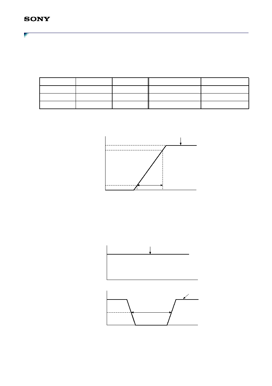
IF Output Signal (DATA_OUT)
(V
CC
1 = V
CC
2 = 1.8V, V
CC
3 = OPEN, Ta = 25
∞
C)
ENABLE Signal
(V
CC
1 = 1.8
± 0.2V, V
CC
1
V
CC
2
3.3V, 2.7V V
CC
3
3.3V, Ta = 25
∞
C)
Power-on Reset Function
(V
CC
1 = 1.8
± 0.2V, V
CC
1
V
CC
2
3.3V, 2.7V V
CC
3
3.3V, Ta = 25
∞
C)
TCXO
(V
CC
1 = V
CC
2 = 1.8V, V
CC
3 = OPEN, Ta = 25
∞
C)
Item
Symbol
Conditions
Min.
Typ.
Max.
Unit
DATA_OUT rise time DTr
Pin 7 (DATA_OUT) 10 to 90%
Load = 1M
//13pF
--
6
--
ns
DATA_OUT fall time
DTf
Pin 7 (DATA_OUT) 10 to 90%
Load = 1M
//13pF
--
4
--
ns
Item
Symbol
Conditions
Min.
Typ.
Max.
Unit
Input voltage high
level
EVIH
Pin 43 (ENABLE) input voltage high
level threshold voltage
1.2
--
V
CC
2
+ 0.2
V
Input voltage low
level
EVIL
Pin 43 (ENABLE) input voltage low level
threshold voltage
≠0.1
--
0.2
V
Item
Symbol
Conditions
Min.
Typ.
Max. Unit
Allowable rise time
MTr
ENABLE and power supply (V
CC
1, V
CC
2) rise
time for the power-on reset function to operate.
Note: Use an ENABLE and power supply
(V
CC
1, V
CC
2) rise time of 100ms or less.
--
--
100
ms
Item
Symbol
Conditions
Min.
Typ.
Max.
Unit
Input level
Vtcxo
Input level to Pin 14 (TCXO)
0.2
0.6
1.2
Vp-p
CLK_OUT rise time
CTr
Pin 13 (CLK_OUT) 10 to 90%
Load = 1M
//13pF
--
6
--
ns
CLK_OUT fall time
CTf
Pin 13 (CLK_OUT) 10 to 90%
Load = 1M
//13pF
--
4
--
ns
CXA3355AER
- 11 -
Threshold Voltage Value
(V
CC
1 = 1.8
± 0.2V, V
CC
1
V
CC
2
3.3V, 2.7V V
CC
3
3.3V, Ta = 25
∞
C)
Threshold Voltage Value (Antenna Sense)
(V
CC
1 = V
CC
2 = 1.8V, V
CC
3 = 3V, Ta = 25
∞
C)
Item
Symbol
Conditions
Min.
Typ.
Max.
Unit
Logic input voltage
high level
V
IH
Logic input pins = Pin 10 (DATA),
Pin 11 (CLK),
Pin 12 (LT)
V
CC
2
≠ 0.2
--
V
CC
2
+ 0.2
V
Logic input voltage
low level
V
IL
Logic input pins = Pin 10 (DATA),
Pin 11 (CLK),
Pin 12 (LT)
≠0.1
--
0.2
V
Logic output voltage
high level
V
OH
Logic output pin = Pin 2 (DIAG)
V
CC
3
≠ 0.2
--
V
CC
3
V
Logic output pins = Pin 7 (DATA_OUT),
Pin 13 (CLK_OUT)
V
CC
2
≠ 0.2
--
V
CC
2
V
Logic output voltage
low level
V
OL
Logic output pins = Pin 7 (DATA_OUT),
Pin 13 (CLK_OUT)
0
--
0.2
V
Item
Symbol
Conditions
Min.
Typ.
Max.
Unit
Threshold voltage 1
Vs1
Threshold voltage at which connection
of the prescribed load is detected from
the open status
10
30
60
mV
Threshold voltage 2
Vs2
Threshold voltage for switching to the
short status from the prescribed load
connected status
140
170
200
mV
CXA3355AER
- 12 -
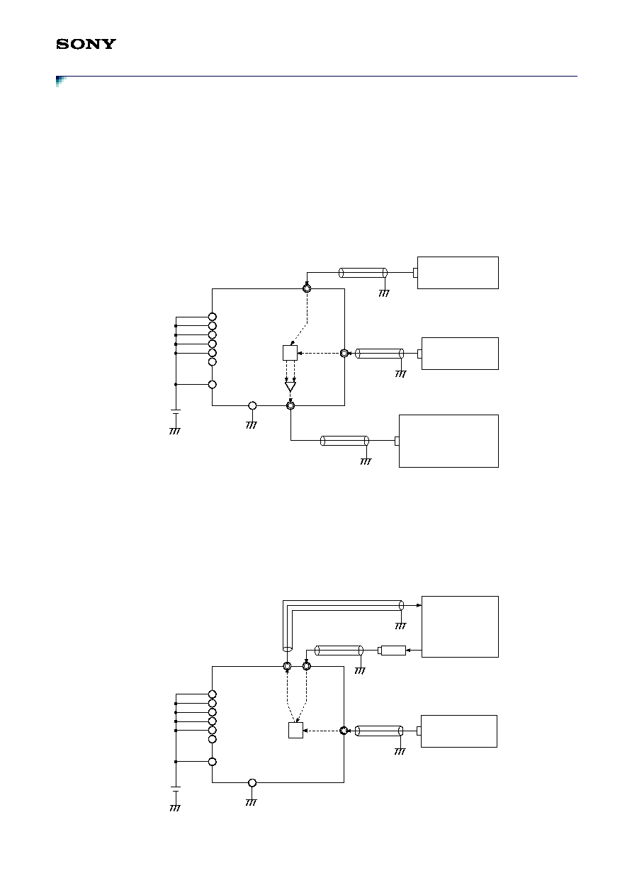
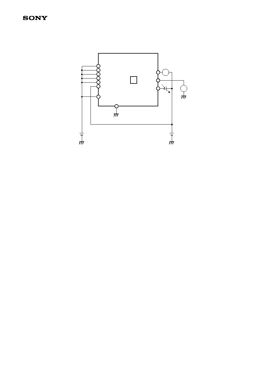
Electrical Characteristics Measurement Circuit
* The RF block bypass capacitors should have excellent high frequency characteristics.
* Use parts with a tolerance of
±1% for the following resistor elements. Other parts should have a tolerance of ±5%.
Pin 17 (LPF)
Pin 42 (R_EXT1)
Pin 44 (R_EXT2)
ENABLE pin
V
CC
2 (IF): Active mode
GND: Power save mode
0.1µ
0.1µ
10p
10n
TCXO input level:
0.2 to 1.2Vp-p
CLK_OUT
V
CC
1 (PLL)
V
CC
1 (LNA)
V
CC
1 (PLL)
V
CC
2 (IF)
V
CC
2 (IF)
V
CC
1 (IF)
V
CC
1 (RF)
10p
8p
100p
24k
12p
12p
LNA_IN
LNA_OUT
RF_IN
3.3p
18n
12n
3p
100p
1p
2.7p
50
matching condition
DIAG
DATA_OUT
ANT
18n
3.9n
4.7n
1n
Bus Control
39k
33k
0.1µ
1n
Buffer
Buffer
TESTIN
TESTOUT
16
17
14
13
15
18
19
20
21
22
23
24
44
43
42
41
40
39
38
37
27
28
29
30
25
26
31
32
33
34
35
36
10
9
8
7
12
11
6
5
4
3
2
1
GND (RF)
GND (RF)
RF_INP
RF_INN
GND
V
CC
1 (LNA)
LNA_OUT
GND
GND
LNA_IN
GND (LNA)
GND (LNA)
GND (LNA)
VCO_I
C_VCO
GND
LPF
V
CC
1 (PLL)
GND (PLL)
TCXO
CLK_OUT
LT
V
CC
1 (RF)
V
CC
1 (RF)
TESTINP
TESTINN
TESTOUTP
TESTOUTN
V
CC
1 (IF)
GND (IF)
R_EXT1
ENABLE
R_EXT2
ASENS
DIAG
AILIM
GND (ANT)
V
CC
3 (ANT)
C_EXT
DATA_OUT
V
CC
2 (IF)
GND (IF)
DATA
CLK
CXA3355AER
- 13 -
Measurement Methods
Note) The measurement methods in 4fo mode (TCXO = 16.368MHz, IF = 4.092MHz) are described below.
1) Total Gain
Input: LNA_IN
Output: TESTOUTP (Pin 38), TESTOUTN (Pin 39) ... [Pins 38 and 39 are differential output.]
Serial data setting: Test output block "4" (IF AMP2 output block) ... See page 20.
Monitor method: (1) Perform differential ≠ single conversion using an external buffer circuit and measure
the output level. ... [Sony recommended method]
(2) Measure Pins 38 and 39 with a differential probe.
* Total Gain: Output level [dBm] ≠ SG input level to LNA_IN [dBm]
2) LNA NF
Input: LNA_IN
Output: LNA_OUT
* Compensate for the evaluation board and coaxial cable loss, and measure the NF value at the IC end.
[Sony recommended measuring instruments]
Noise source: Agilent 346A
NF meter: Agilent N8973A
Spectrum Analyzer
Center freq. = 4.092MHz
SPAN = 10kHz
RBW = 100Hz
VBW = 100Hz
LNA_IN
TESTOUT
50
50
50
Signal Generator
freq. = 16.368MHz
AMP. = 0dBm
TCXO
Signal Generator
freq. = 1575.42MHz
AMP. = ≠120dBm
External
buffer
V
CC
1 (RF)
V
CC
= 1.8V
ENABLE
V
CC
1 (IF)
V
CC
2 (IF)
V
CC
3 (ANT)
V
CC
1 (PLL)
V
CC
1 (LNA)
TESTOUTP
TESTOUTN
OPEN
GND
Evaluation
Board
Microwave coaxial cable
Microwave coaxial cable
Microwave coaxial cable
IC
All GND pins
LNA_IN
LNA_OUT
50
Noise Source
Signal Generator
freq. = 16.368MHz
AMP. = 0dBm
TCXO
freq. = 1575.42MHz
BW = 2MHz
NF meter
V
CC
1 (RF)
V
CC
= 1.8V
ENABLE
V
CC
1 (IF)
V
CC
2 (IF)
V
CC
3 (ANT)
V
CC
1 (PLL)
V
CC
1 (LNA)
OPEN
GND
IC
Microwave coaxial cable
Microwave coaxial cable
Microwave coaxial cable
Evaluation
Board
All GND pins

CXA3355AER
- 14 -
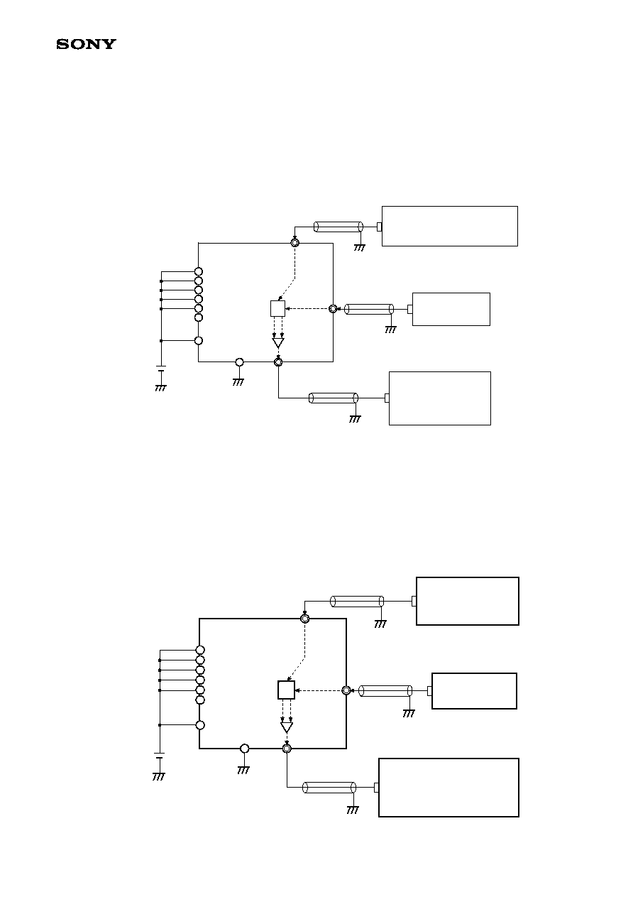
3) Total NF
Input: LNA_IN
Output: TESTOUTP (Pin 38), TESTOUTN (Pin 39) ... [Pins 38 and 39 are differential output.]
Serial data setting: Test output block "3" (IF filter output block) ... See page 20.
Monitor method: (1) Perform differential ≠ single conversion using an external buffer circuit and measure
the output level. ... [Sony recommended method]
(2) Measure Pins 38 and 39 with a differential probe.
* Total NF: Calculate NF from the noise power ratio when the DC 28V applied to the noise source is
switched on and off.
Use the 346A made by Agilent as the noise source for measurement.
NF calculation formula
Y = N
ON
/N
OFF
NF = 10 log (ENR/(Y ≠ 1))
N
ON
: Noise power when the DC 28V is on.
N
OFF
: Noise power when the DC 28V is off.
ENR: Excess Noise Ratio
4) P-1dB Input
Input: LNA_IN
Output: TESTOUTP (Pin 38), TESTOUTN (Pin 39) ... [Pins 38 and 39 are differential output.]
Serial data setting: Test output block "4" (IF AMP2 output block) ... See page 20.
Monitor method: (1) Perform differential ≠ single conversion using an external buffer circuit and measure
the output level. ... [Sony recommended method]
(2) Measure Pins 38 and 39 with a differential probe.
* P-1dB Input: Input level [dBm] at the point when the response drops by 1dB from the desired signal
straight line extension.
Spectrum Analyzer
Center freq. = 4.092MHz
SPAN = 10kHz
RBW = 100Hz
VBW = 100Hz
LNA_IN
TESTOUT
50
50
Signal Generator
freq. = 16.368MHz
AMP. = 0dBm
TCXO
External
buffer
V
CC
1 (RF)
V
CC
= 1.8V
DC 28V
ON/OFF
ENABLE
V
CC
1 (IF)
V
CC
2 (IF)
V
CC
3 (ANT)
V
CC
1 (PLL)
V
CC
1 (LNA)
TESTOUTP
TESTOUTN
OPEN
GND
IC
Noise Source
Microwave coaxial cable
Microwave coaxial cable
Evaluation
Board
All GND pins
Spectrum Analyzer
Center freq. = 4.092MHz
SPAN = 10kHz
RBW = 100Hz
VBW = 100Hz
LNA_IN
TESTOUT
50
50
50
Signal Generator
freq. = 16.368MHz
AMP. = 0dBm
TCXO
Signal Generator
freq. = 1575.42MHz
AMP. = ≠120 to ≠90dBm
External
buffer
V
CC
1 (RF)
V
CC
= 1.8V
ENABLE
V
CC
1 (IF)
V
CC
2 (IF)
V
CC
3 (ANT)
V
CC
1 (PLL)
V
CC
1 (LNA)
TESTOUTP
TESTOUTN
OPEN
GND
IC
Microwave coaxial cable
Microwave coaxial cable
Microwave coaxial cable
Evaluation
Board
All GND pins
CXA3355AER
- 15 -
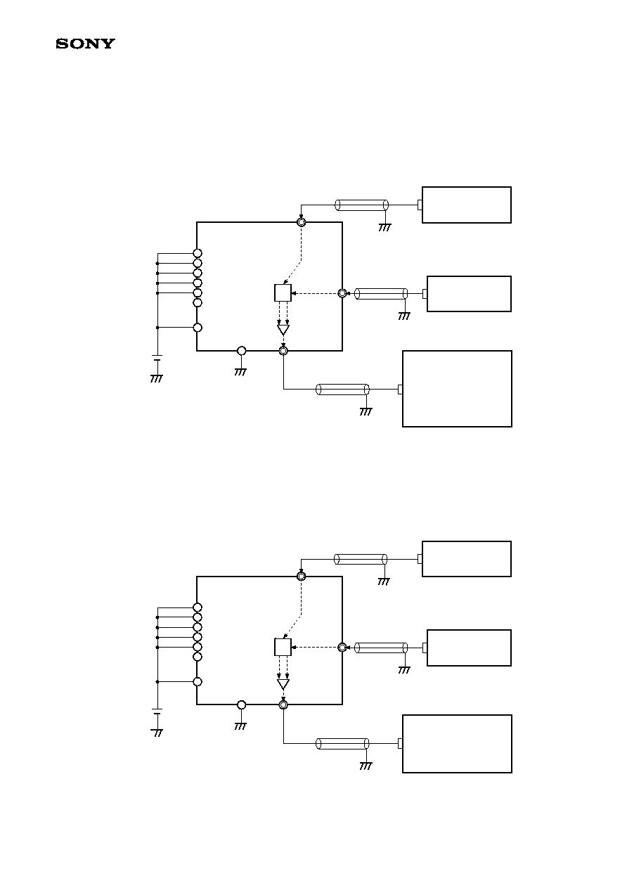
5) Image Rejection Ratio
Input: LNA_IN
Output: TESTOUTP (Pin 38), TESTOUTN (Pin 39) ... [Pins 38 and 39 are differential output.]
Serial data setting: Test output block "2" (Adder output block) ... See page 20.
Monitor method: (1) Perform differential ≠ single conversion using an external buffer circuit and measure
the output level. ... [Sony recommended method]
(2) Measure Pins 38 and 39 with a differential probe.
* IMRR (detuning frequency
4MHz): Image wave output level (at 1575.42MHz input) [dBm] ≠
Desired wave output level (at 1567.236MHz input) [dBm]
6) Filter Response
Input: LNA_IN
Output: TESTOUTP (Pin 38), TESTOUTN (Pin 39) ... [Pins 38 and 39 are differential output.]
Serial data setting: Test output block "3" (IF filter output block) ... See page 20.
Monitor method: (1) Perform differential ≠ single conversion using an external buffer circuit and measure
the output level. ... [Sony recommended method]
(2) Measure Pins 38 and 39 with a differential probe.
* Filter Response: Vary the input frequency to LNA_IN and measure the output level. Normalize fo (4fo) to
the reference (0dB).
Spectrum Analyzer
Center freq. = 4.092MHz
SPAN = 10kHz
RBW = 100Hz
VBW = 100Hz
LNA_IN
TESTOUT
50
50
50
Signal Generator
freq. = 16.368MHz
AMP. = 0dBm
TCXO
Signal Generator
freq. = 1575.42MHz (Desired wave)
1567.236MHz (Image wave)
AMP. = ≠75dBm
External
buffer
V
CC
1 (RF)
V
CC
= 1.8V
ENABLE
V
CC
1 (IF)
V
CC
2 (IF)
V
CC
3 (ANT)
V
CC
1 (PLL)
V
CC
1 (LNA)
TESTOUTP
TESTOUTN
OPEN
GND
IC
Microwave coaxial cable
Microwave coaxial cable
Microwave coaxial cable
Evaluation
Board
All GND pins
Spectrum Analyzer
Center freq. = 150kHz to 100MHz
SPAN = 10kHz
RBW = 100Hz
VBW = 100Hz
LNA_IN
TESTOUT
50
50
50
Signal Generator
freq. = 16.368MHz
AMP. = 0dBm
TCXO
Signal Generator
freq. = 1571.388MHz to
1675.42MHz
AMP. = ≠75dBm
External
buffer
V
CC
1 (RF)
V
CC
= 1.8V
ENABLE
V
CC
1 (IF)
V
CC
2 (IF)
V
CC
3 (ANT)
V
CC
1 (PLL)
V
CC
1 (LNA)
TESTOUTP
TESTOUTN
OPEN
GND
IC
Microwave coaxial cable
Microwave coaxial cable
Microwave coaxial cable
Evaluation
Board
All GND pins
CXA3355AER
- 16 -
7) C/N
Input: LNA_IN
Output: TESTOUTP (Pin 38), TESTOUTN (Pin 39) ... [Pins 38 and 39 are differential output.]
Serial data setting: Test output block "1I" (Ich mixer output block) ... See page 20.
Monitor method: (1) Perform differential ≠ single conversion using an external buffer circuit and measure
the output level. ... [Sony recommended method]
(2) Measure Pins 38 and 39 with a differential probe.
* C/N: Carrier + 100kHz noise level ≠ Carrier level [dBc/Hz]
8) Spurious
Input: LNA_IN
Output: TESTOUTP (Pin 38), TESTOUTN (Pin 39) ... [Pins 38 and 39 are differential output.]
Serial data setting: Test output block "4" (IF AMP2 output block) ... See page 20.
Measure the spurious components separated by a certain frequency from the carrier.
* Spurious: Each spurious output level ≠ Carrier level [dBc]
Spectrum Analyzer
Center freq.
(Carrier) = 4.092MHz
(Noise) = 4.192MHz
SPAN = 10kHz
RBW = 100Hz
VBW = 100Hz
LNA_IN
TESTOUT
50
50
50
Signal Generator
freq. = 16.368MHz
AMP. = 0dBm
TCXO
Signal Generator
freq. = 1575.42MHz
AMP. = ≠60dBm
External
buffer
V
CC
1 (RF)
V
CC
= 1.8V
ENABLE
V
CC
1 (IF)
V
CC
2 (IF)
V
CC
3 (ANT)
V
CC
1 (PLL)
V
CC
1 (LNA)
TESTOUTP
TESTOUTN
OPEN
GND
IC
Microwave coaxial cable
Microwave coaxial cable
Microwave coaxial cable
Evaluation
Board
All GND pins
Spectrum Analyzer
Center freq. = 4.092MHz
SPAN = 10kHz
RBW = 100Hz
VBW = 100Hz
LNA_IN
TESTOUT
50
50
50
Signal Generator
freq. = 16.368MHz
AMP. = 0dBm
TCXO
Signal Generator
freq. = 1575.52MHz
AMP. = ≠120dBm
External
buffer
V
CC
1 (RF)
V
CC
= 1.8V
ENABLE
V
CC
1 (IF)
V
CC
2 (IF)
V
CC
3 (ANT)
V
CC
1 (PLL)
V
CC
1 (LNA)
TESTOUTP
TESTOUTN
OPEN
GND
All GND pins
IC
Microwave coaxial cable
Microwave coaxial cable
Microwave coaxial cable
Evaluation
Board
CXA3355AER
- 17 -
9) Antenna Sense
Vary V
S
and measure the DIAG pin voltage.
Vary V
S
and measure the inflow current Ib to AILIM.
V
CC
1 (RF)
AILIM
DIAG
ASENS
Vs
V
CC
= 1.8V
V
CC
3 = 3.0V
ENABLE
V
CC
1 (IF)
V
CC
2 (IF)
V
CC
3 (ANT)
V
CC
1 (PLL)
V
CC
1 (LNA)
GND
All GND pins
IC
V
A
Evaluation
Board
CXA3355AER
- 18 -
Initial Settings
The CXA3355AER is initialized by setting the ENABLE signal (Pin 43) from low level to high level.
The timing, etc. should satisfy the conditions below.
In addition, the TCXO frequency and IF frequency combinations in the table below can be obtained by setting
Pin 10 (DATA), Pin 11 (CLK) and Pin 12 (LT) as shown in the table and then performing initialization. This
eliminates the need for serial data setting.
1. During Power-on
The CXA3355AER is initialized by simultaneously raising the power supplies and the ENABLE signal (Pin 43)
during power-on. The power supply and ENABLE signal (Pin 43) rise time should be 100ms or less.
In addition, the power supplies (V
CC
1, V
CC
2) should rise simultaneously. The antenna sense circuit power
supply (V
CC
3) should be left open except when using the antenna sense function.
2. Initialization After Power-on
After power-on, the CXA3355AER is initialized by setting the ENABLE signal (Pin 43) to low level for 10ms or
more and then setting it to high level.
Pin 10 (DATA)
Pin 11 (CLK)
Pin 12 (LT)
TCXO frequency [MHz]
IF frequency [MHz]
GND
GND
GND
16.368
4.092
V
CC
2
GND
GND
18.414
1.023
V
CC
2
V
CC
2
GND
13
0.976
V
CC
0.9
◊ V
CC
0.1
◊ V
CC
GND
100ms or less
Power supply, ENABLE
V
CC
GND
Power supply
V
CC
GND
10ms or more
0.5
◊ V
CC
ENABLE
CXA3355AER
- 19 -
Serial Data Settings
The CXA3355AER can make the PLL counter settings, perform TCXO_CLK output, select the internal IF filter,
and use the test I/O circuit according to the serial data settings (3-wire bus control). The transfer bit length is
18 bits, and there are four addresses. The address is set by the A1 and A0 bits. The timing, etc. should satisfy
the conditions below.
Serial Data Format
MC (0 to 10): Main counter frequency division value setting
0: Logic input voltage low level
SC (0 to 4): Swallow counter frequency division value setting
1: Logic input voltage high level
RC (0 to 8): Reference counter
CLK: TCXO CLK output (0: Not output, 1: Output)
FIL: Internal filter selection (0: fo mode LPF, 1: 4fo mode BPF)
TCL: IF block test I/O control (0: When not using the test I/O circuit, 1: When using the test I/O circuit)
TI (0 to 2): IF block test input location setting
TO (0 to 2): IF block test output location setting
18-bit Data Format
Serial Data Interface Bus Timing (3-wire Bus Control)
MSB
LSB
A1
A0
D15 D14 D13 D12 D11 D10
D9
D8
D7
D6
D5
D4
D3
D2
D1
D0
0
0
MC10 MC9 MC8 MC7 MC6 MC5 MC4 MC3 MC2 MC1 MC0
0
0
0
CLK
0
0
1
SC4 SC3 SC2 SC1 SC0 RC8 RC7 RC6 RC5 RC4 RC3 RC2 RC1 RC0
0
TCL
1
0
TI2
TI1
TI0 TO2 TO1 TO0
0
0
0
0
0
0
0
0
FIL
0
1
1
0
0
0
0
0
0
0
0
0
0
0
0
0
0
0
0
A1
A0
D15
D14
D13
D12
D11
D10
D9
D8
D7
D6
D5
D4
D3
D2
D1
D0
DATA
CLK
LT
Latch
Invalid data
Invalid data
Address
data
Each data
Input data to all four addresses.
Time
t
SD
t
HD
t
HL
t
WHLT
CLK
DATA
LT
t
LOW
t
HIGH
t
SD
= Data setup time
t
HD
= Data hold time
t
LOW
= Low period of CLK
t
HIGH
= High period of CLK
t
SL
= LT setup time
t
WHLT
= High pulse width (LT)
t
WHLT
100ns
t
SD
, t
HD
, t
LOW
, t
HIGH
, t
HL
, t
WHLT
50ns
CXA3355AER
- 20 -
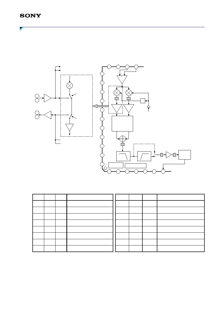
Description of Functions
1. Test Circuit
The CXA3355AER has a test circuit for test signal I/O. The test circuit is connected between each IF block,
and test I/O control can be performed by the serial data settings. The test circuit location, configuration and the
serial data settings are as follows.
Test Circuit Location and Configuration
0: Logic input voltage low level
1: Logic input voltage high level
* Set the TCL register to "1" when using or to "0" when not using the test input circuit or the test output circuit.
(See page 20.)
Serial Data Settings for Test Input Selection
Serial Data Settings for Test Output Selection
TI2
TI1
TI0
Test input block
TO2
TO1
TO0
Test output block
0
0
0
Normal operation
0
0
0
Normal operation
0
0
1
Ich IF AMP1 input block
0
0
1
Ich mixer output block
0
1
0
Qch IF AMP1 input block
0
1
0
Qch mixer output block
0
1
1
Not used.
0
1
1
Not used.
1
0
0
Not used.
1
0
0
Not used.
1
0
1
IF filter input block
1
0
1
Adder output block
1
1
0
IF AMP2 input block
1
1
0
IF filter output block
1
1
1
A/D converter input block
1
1
1
IF AMP2 output block
44
43
42
41
40
39
38
37
30
31
32
33
34
35
36
36
37
38
39
7
6
5
4
3
2
1
1540fo = 1575.42MHz
ANT SENSE
Local
IF_AMP1
RF_AMP
IF_AMP1
Mixer
Mixer
"1I"
"1Q"
LPF
HPF
BIAS
IF Phase Shifter
A/D
Converter
IF_AMP2
90∞
"2"
"3"
"4"
Test input control
Test output control
Actual operation is differential, but only one side is shown.
The inter-circuit connections are cut off during test input
selection and test output selection.
From each IF block
To each IF block
"1I": Ich mixer output block (Ich IF AMP1 input block)
"1Q": Qch mixer output block (Qch IF AMP1 input block)
"2": Adder output block (IF filter input block)
"3": IF filter output block (IF AMP2 input block)
"4": IF AMP2 output block (A/D converter input block)
CXA3355AER
- 21 -
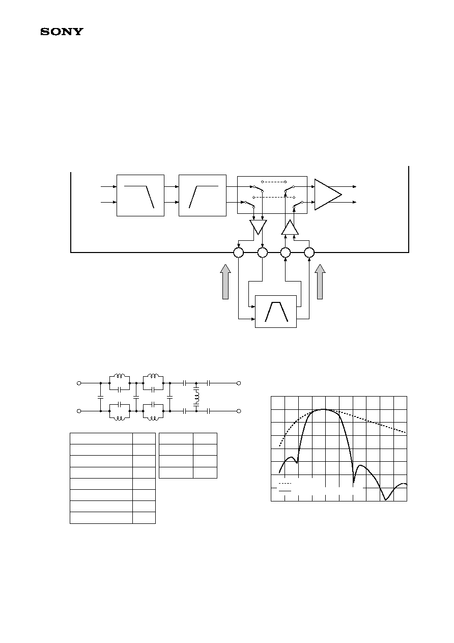
2. Using an External Filter
When using the CXA3355AER in 4fo mode with the initial settings (see page 18) which do not require serial
data setting, input and output are performed via the test circuit located between the internal IF filter and the IF
AMP2 in the following stage, so an external filter is necessary.
The external filter uses Pins 36 to 39. Differential I/O is performed with Pin 38 (TESTOUTP) and Pin 39
(TESTOUTN) as the internal IF filter output pins and Pin 36 (TESTINP) and Pin 37 (TESTINN) as the input
pins to IF AMP2. Also, the impedance is 200
(differential) for both input and output.
Note that the bias voltage is determined inside the IC, so Pins 36 and 37 should not be connected directly with
Pins 38 and 39. When not using an external filter, eliminate the DC components using an approximately 10nF
capacitor.
The overall external filter block and the external filter configuration are shown below.
Overall External Filter Block
External Filter Configuration
39
38
37
36
Pin 36: TESTINP
Pin 37: TESTINN
Pin 38: TESTOUTP
Pin 39: TESTOUTN
LPF
HPF
To the comparator
CXA3355AER
External filter
Secondary LPF
Secondary HPF
External filter I/O circuit
IF AMP2
Zout
200
Zin
200
Internal filter
Internal filter + External filter
CXA3355AER IF Filter Response
(Example of representative characteristics)
Normalized at 4MHz
≠70
≠60
≠50
≠40
≠30
≠20
≠10
0
10
0
1
2
3
4
5
6
7
8
9
10
Detuning frequency [MHz]
Response [dB]
Pin 38
Pin 39
Pin 37
Pin 36
C1
C3
L1
L2
C5
L3
C4
C6
L4
C7
C8
C9
C12
C13
C10
C11
L5, L6
(2 series)
C2
Chip C
C1
C2, C3
C4
C5, C6
C7
C8, C9, C12, C13
C10, C11
[pF]
91
300
240
91
130
680
1500
Chip L
L1, L2
L3, L4
L5, L6
[µH]
2.2
3.9
4.7
CXA3355AER
- 22 -
Description of Operation
Overview of Operation
This IC down-converts the GPS (Global Positioning System) frequency of 1.57542GHz to fo (fo: 1.023MHz) or
4fo (4fo: 4.092MHz).
The internal configuration is divided into the analog block, consisting of the amplifier, mixer and filters, and the
digital block (including the comparator block and the control block), which forms the PLL.
The analog block converts the frequency and amplifies the signal with the amplifier and the mixer, and
eliminates undesired components with the filters.
The digital block can switch the PLL frequency division ratio in order to down convert the output signal to fo or
4fo.
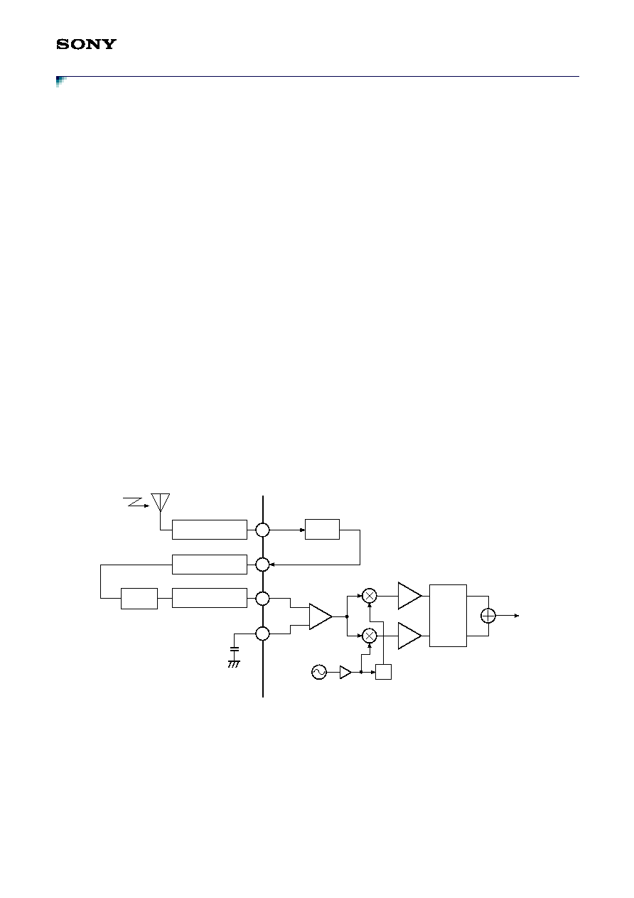
1. LNA
The GPS signal that passes through the antenna is input to Pin 24 via a matching circuit as shown in the
figure below.
The input signal is amplified by the LNA, and then output from Pin 27.
Always use matching circuits for the LNA input pin (Pin 24) and the LNA output pin (Pin 27), and match at
1.57542GHz.
2. RF Amplifier, RF Mixer, IF Phase Shifter and Adder
The signal amplified by the LNA passes through the SAW filter, and is then input to Pin 30 via a matching
circuit.
The input signal is amplified by the RF amplifier, and then down-converted by the RF mixer to the fo
(1.023MHz) or 4fo (4.092MHz) I and Q components. The IF signal down-converted to the I and Q
components has the image component eliminated by the phase shifter and the adder, and is then input to
the IF filter.
Always use a matching circuit for the RF amplifier input pin (Pin 30), and match at 1.57542GHz.
31
30
27
24
LNA
1540fo
0∞
90∞
To the IF filter
fo or 4fo
Adder
fo: 1.023MHz
SAW
Matching Circuit
90∞
Matching Circuit
Matching Circuit
Phase
Shifter
CXA3355AER
- 23 -
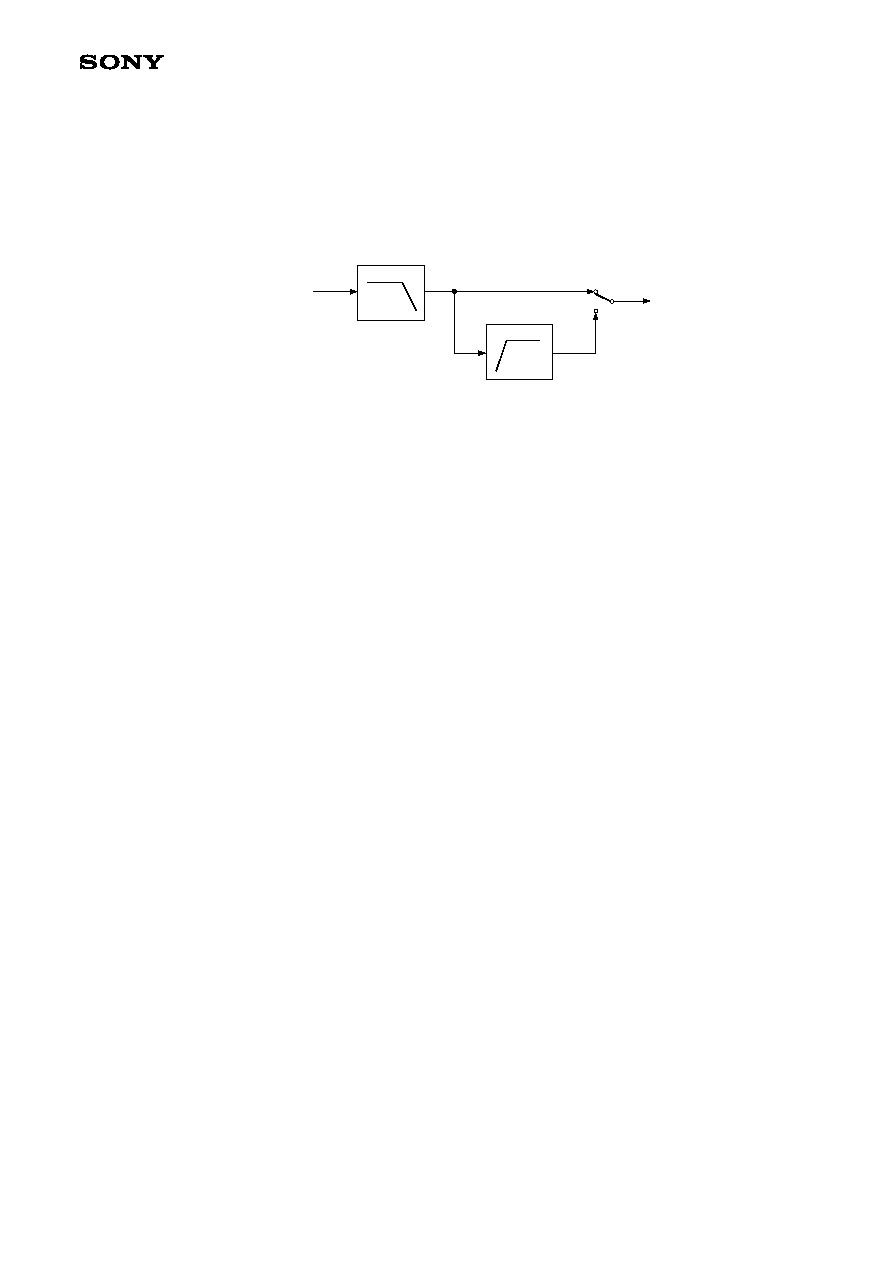
3. IF Filter
The IF signal that passed through the adder has the undesired components outside the band eliminated by
the IF filter.
In fo mode the signal passes through only the LPF and is input to IF AMP2. In 4fo mode the signal passes
through the LPF and then the HPF and is input to IF AMP2.
Note that fo mode and 4fo mode can be switched by the serial data setting.
Set the serial data setting register FIL to "0" for fo mode (LPF) or to "1" for 4fo mode (BPF).
In addition, an external filter can also be connected to this IC using Pins 36 to 39. (See page 21.)
4. IF AMP2 and A/D Converter
The signal that passed through the IF filter is amplified by IF AMP2, converted to a binary signal by the A/D
converter, and then output from the DATA output pin (Pin 7). The A/D converter performs sampling at the
TCXO CLK.
In addition, the A/D converter output voltage high level is V
CC
2 (1.6 to 3.3V), so a wide range of interfaces
can be supported.
5. TCXO (Pin 14)
Input the signal from the external oscillator to Pin 14 via a capacitor as the reference signal. Input
frequencies from 10MHz to 26MHz are supported. The input signal level from the external oscillator should
be 1.2Vp-p or less (0.6Vp-p typ., 0.2Vp-p min.). This is also the same in power save mode. However, using
the typical level of 0.6Vp-p is recommended from the viewpoint of reducing harmful waves to the receive
block, etc.
6. TCXO CLK Output (Pin 13)
This IC can output TCXO CLK from Pin 13 according to the serial data setting. The output voltage high level
is V
CC
2 (1.6 to 3.3V), so a wide range of interfaces can be supported.
Set the serial data setting register CLK to "0" when not using TCXO CLK, or to "1" when using TCXO CLK.
(See page 19.)
To IF AMP2
From the adder
LPF
HPF
CXA3355AER
- 24 -
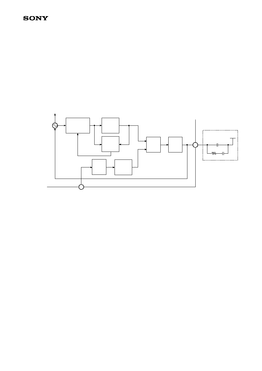
7. PLL/VCO
The PLL is comprised by a VCO, frequency divider and phase/frequency comparator as shown in the figure
below, and incorporates an inductor, varactor and all other necessary components. The loop filter is
externally connected. Use components that satisfy the required characteristics.
Serial data setting is unnecessary when this IC is used with the typical TCXO and IF combinations set by
the initial settings shown in page 18.
When making serial data settings, set counter frequency division values that satisfy the following equations.
f
VCO
= (M
◊ N + A) ◊ (f
TCXO
◊ 2)/R
(f
TCXO
◊ 2)/R > 800kHz
N
3, R 3
f
VCO
: VCO oscillation frequency, f
TCXO
: TCXO frequency
MC data = N, SC data = A, RC data = R, DMPS data = M = 24 (fixed)
8. ENABLE (Pin 43)
Active mode and power save mode can be switched according to the level.
High (V_IH: 1.2V min.): Active mode
Low (V_IL: 0.2V max.): Power save mode
17
14
MC
1/N
SC
1/A
RC
1/R
PFD
CP
Frequency division ratio (M
◊ N) + A
TCXO (10MHz to 26MHz)
To the RF phase shifter
Loop filter
◊2
V
CC
1
M = 24
VCO
DMPS
1/M, 1/(M + 1)

CXA3355AER
- 25 -
9. Antenna Sense
The power supply lines are separated internally, so antenna sense operation at the supply voltage (V
CC
3)
of 3.0
± 0.3V is recommended. Note that the antenna sense function does not operate independently, so
voltage should also be applied to the other power supply pins (V
CC
1, V
CC
2) for use in active mode. In
addition, leave the power supply pin (V
CC
3) open when not using the antenna sense function.
The antenna sense function checks whether an antenna is connected. Pin 2 (DIAG) outputs high voltage
when an antenna is not connected, or low voltage when an antenna is connected. A current limiting circuit
is provided as a countermeasure against short circuits.
The DIAG pin voltage switching point is as shown in the table below.
V1, V2, V3 and Ib in the table below are as follows.
V1: 10 to 60mV
Threshold voltage at which connection of the prescribed load is detected from the
open status
V2: 140 to 200mV
Threshold voltage for switching to the short status from the prescribed load
connected status.
V3: 250mV
Current limiting threshold voltage.
Ib: 1.7 to 2.1mA
Base current in the normal connection status.
Antenna Sense Block Circuit
3
1
2
R3
DIAG
Ib
V
CC
3 (ANT)
V
CC
3 (ANT)
V1
V2
V3
A1
A2
A3
VD
VA
Vs
CXA3355AER
ASENS
AILIM
DIAG [V]
V1
V2
Vs
Ib [mA]
V3
Vs
I1
I1 = 1.9mA
(Typ.)
MODE
Vs < V1
V1 < Vs < V2
V2 < Vs
Connection status
Open
Normal connection
Short
DIAG voltage
High
Low
High
CXA3355AER
- 26 -
Application Circuit
* This diagram shows the application circuit when the initial settings are made for 4fo mode. (See page 18.)
* The RF block bypass capacitors should have excellent high frequency characteristics.
* Use parts with a tolerance of
±1% for the following resistor elements. Other parts should have a tolerance of
±5%.
Pin 17 (LPF)
Pin 42 (R_EXT1)
Pin 44 (R_EXT2)
ENABLE pin
Vcc2 (IF): Active mode
GND: Power save mode
0.1µ
0.1µ
10p
10n
TCXO input level:
0.2 to 1.2Vp-p
V
CC
1 (PLL)
V
CC
1 (LNA)
SAW Filter
V
CC
1
(LNA)
V
CC
1
(RF)
V
CC
1
(IF)
V
CC
1
(PLL)
V
CC
2
(IF)
V
CC
1 (PLL)
V
CC
2 (IF)
V
CC
2 (IF)
V
CC
1 (IF)
V
CC
1 (RF)
10p
8p
100p
24k
12p
12p
3.3p
18n
12n
3p
100p
1p
2.7p
DATA_OUT
18n
3.9n
4.7n
1n
39k
33k
1n
10n
10n
16
17
14
13
15
18
19
20
21
22
23
24
44
43
42
41
40
39
38
37
27
28
29
30
25
26
31
32
33
34
35
36
10
9
8
7
12
11
6
5
4
3
2
1
GND (RF)
GND (RF)
RF_INP
RF_INN
GND
V
CC
1 (LNA)
LNA_OUT
GND
GND
LNA_IN
GND (LNA)
GND (LNA)
GND (LNA)
VCO_I
C_VCO
GND
LPF
V
CC
1 (PLL)
GND (PLL)
TCXO
CLK_OUT
LT
V
CC
1 (RF)
V
CC
1 (RF)
TESTINP
TESTINN
TESTOUTP
TESTOUTN
V
CC
1 (IF)
GND (IF)
R_EXT1
ENABLE
R_EXT2
ASENS
DIAG
AILIM
GND (ANT)
V
CC
3 (ANT)
C_EXT
DATA_OUT
V
CC
2 (IF)
GND (IF)
DATA
CLK
0.1µ
1µ
V
CC
= 1.8V
Number of parts
∑ Resistors: 3pcs
∑ Capacitors: 20pcs
∑ Inductors: 5pcs
∑ SAW filter: 1pcs
(Excluding the antenna sense circuit)
Application circuits shown are typical examples illustrating the operation of the devices. Sony cannot assume responsibility for
any problems arising out of the use of these circuits or for any infringement of third party patent and other right due to same.
CXA3355AER
- 27 -
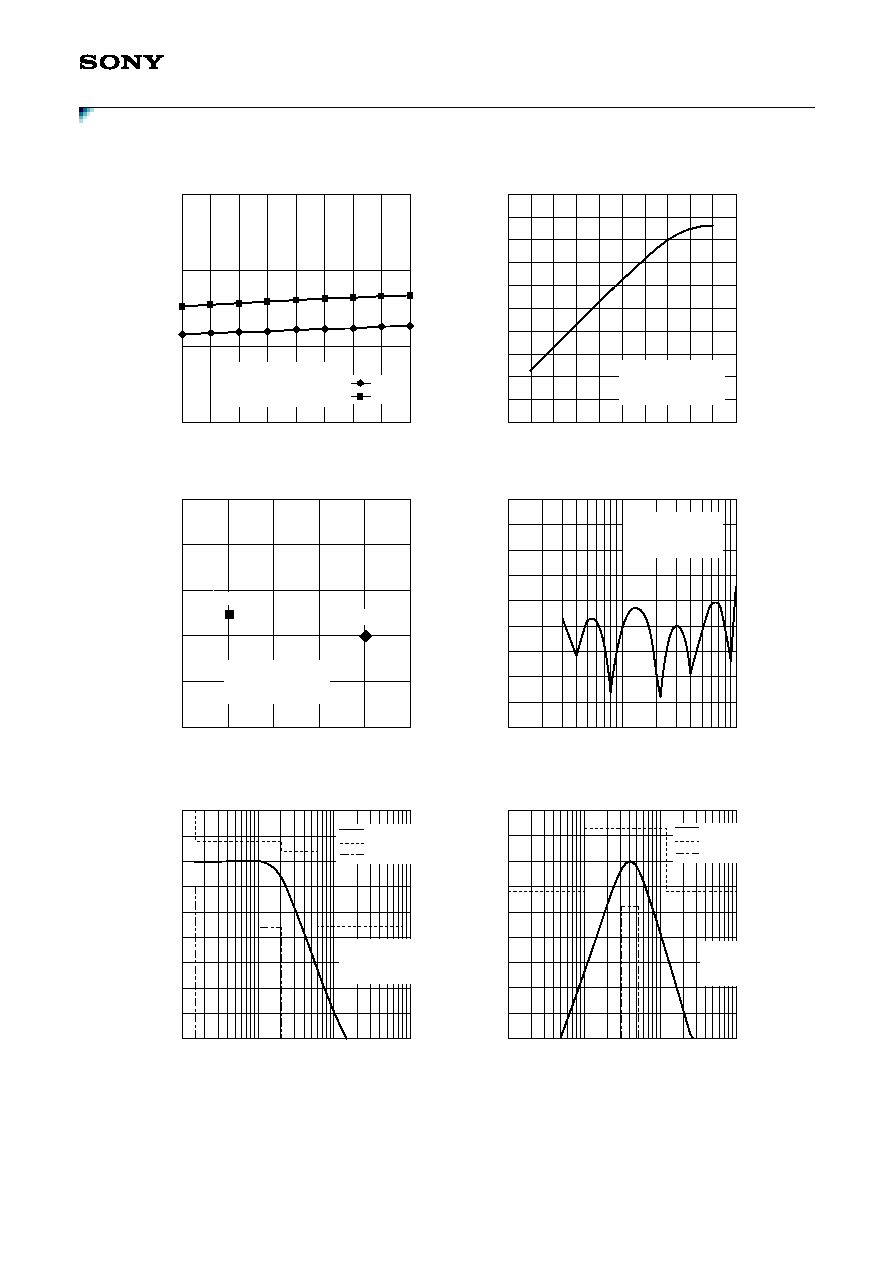
Supplement Materials (Example of representative characteristics)
≠35
≠30
≠25
≠20
≠15
≠10
≠5
0
5
10
0.1
1
10
100
Detuning frequency [MHz]
Filter response [dB]
fo
Upper spec (fo)
Lower spec (fo)
≠35
≠30
≠25
≠20
≠15
≠10
≠5
0
5
10
0.1
1
10
100
Detuning frequency [MHz]
Filter response [dB]
4fo
Upper spec (4fo)
Lower spec (4fo)
≠40
≠35
≠30
≠25
≠20
≠15
≠10
≠5
0
5
10
≠135 ≠130 ≠125 ≠120 ≠115 ≠110 ≠105 ≠100 ≠95 ≠90 ≠85
LNA_IN input level [dBm]
IF AMP2 output level [dBm]
5
10
15
20
1.60 1.65 1.70 1.75 1.80 1.85 1.90 1.95 2.00
Vcc [V]
Icc [mA]
fo
4fo
0
2
4
6
8
10
0
1
2
3
4
5
IF frequency [MHz]
Total NF [dB]
≠65
≠60
≠55
≠50
≠45
≠40
≠35
≠30
≠25
≠20
0.1
1
10
Detuning frequency [MHz]
IMRR [dBc]
Graph 1. I
CC
Graph 2. Total Gain
Graph 5. Filter Response (Normalized at 1.023MHz)
V
CC
1 = V
CC
2 = 1.8V
V
CC
3 = Open
Temp = 25∞C
Graph 6. Filter Response (Normalized at 4.092MHz)
Graph 3. Total NF
Graph 4. Image Rejection Ratio
4fo mode
fo mode
V
CC
1 = V
CC
2 = 1.8V
V
CC
3 = Open
Temp = 25∞C
V
CC
1 = V
CC
2 = 1.8V
V
CC
3 = Open
Temp = 25∞C
V
CC
1 = V
CC
2 = 1.8V
V
CC
3 = Open
Temp = 25∞C
V
CC
1 = V
CC
2 = 1.8V
V
CC
3 = Open
Temp = 25∞C
V
CC
1 = V
CC
2 = 1.8V
V
CC
3 = Open
Temp = 25∞C
CXA3355AER
- 28 -
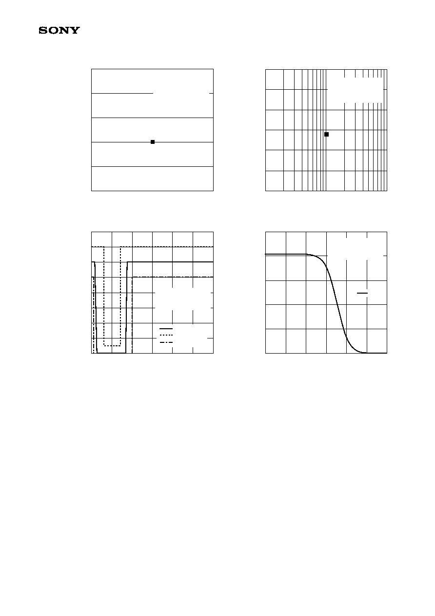
0
0.5
1.0
1.5
2.0
2.5
0
0.1
0.2
0.3
0.4
0.5
0.6
Vs [V]
Ib [mA]
Ib
0
0.5
1.0
1.5
2.0
2.5
3.0
3.5
4.0
0
0.1
0.2
0.3
0.4
0.5
0.6
Vs [V]
DIAG [V]
DIAG
Upper Spec
Lower Spec
≠100
≠90
≠80
≠70
≠60
≠50
≠40
0.01
0.1
1
Frequency difference from the carrier [MHz]
C/N [dBc/Hz]
≠85
≠80
≠75
≠70
≠65
≠60
Evaluation board LNA_IN pin
Local leak [dBm]
Graph 9a. Antenna Sense (V
S
vs. DIAG)
Graph 9b. Antenna Sense (V
S
vs. Ib)
Graph 7. Local Leak
V
CC
1 = V
CC
2 = 1.8V
V
CC
3 = Open
Temp = 25∞C
Graph 8. C/N
V
CC
1 = V
CC
2 = 1.8V
V
CC
3 = Open
Temp = 25∞C
V
CC
1 = V
CC
2 = 1.8V
V
CC
3 = 3V
Temp = 25∞C
V
CC
1 = V
CC
2 = 1.8V
V
CC
3 = 3V
Temp = 25∞C
CXA3355AER
- 29 -
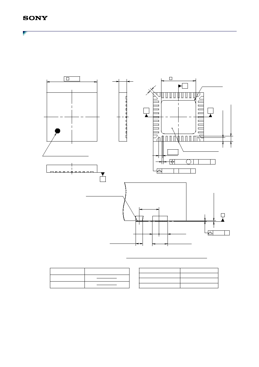
Sony Corporation
Package Outline
(Unit: mm)
44PIN VQFN (PLASTIC)
5.1
0.8 ± 0.1
0.22
3.5
4 - R0.3
C
B
A
23
33
22
34
44
12
1
PIN 1 INDEX
S
0.4
0.4
± 0.1
0.55
± 0.1
Thermal Die Pad
0.1 S A - B C
A - B C
S
M
0.05
X4
Solder Plating
0.4
0.135
0.175
+ 0.09
0.14
≠ 0.03
+ 0.09
0.31
≠ 0.03
0.05
S
S
MAX0.02
TERMINAL SECTION
SONY CODE
JEITA CODE
JEDEC CODE
VQFN-44P-03
PACKAGE MATERIAL
LEAD TREATMENT
LEAD MATERIAL
PACKAGE MASS
EPOXY RESIN
SOLDER PLATING
COPPER ALLOY
0.06g
AP-4000-44010S Rev.2