 | –≠–Ľ–Ķ–ļ—ā—Ä–ĺ–Ĺ–Ĺ—č–Ļ –ļ–ĺ–ľ–Ņ–ĺ–Ĺ–Ķ–Ĺ—ā: CXA3562R | –°–ļ–į—á–į—ā—Ć:  PDF PDF  ZIP ZIP |

≠ 1 ≠
E01115-PS
Sony reserves the right to change products and specifications without prior notice. This information does not convey any license by
any implication or otherwise under any patents or other right. Application circuits shown, if any, are typical examples illustrating the
operation of the devices. Sony cannot assume responsibility for any problems arising out of the use of these circuits.
CXA3562R
100 pin LQFP (Plastic)
Description
The CXA3562R is a driver IC developed for use
with Sony polycrystalline silicon TFT LCD panels. It
supports digital 2-parallel and single input, and the
input data is analog demultiplexed into 12 phases and
output. The CXA3562R can directly drive an LCD
panel, and the VCOM setting circuit and precharge
pulse waveform generator are also on-chip.
Features
∑ Supports 10-bit 2-parallel and single input
∑ Supports signals up to UXGA
(1/2 clock when using UXGA signals)
∑ Low output deviation by on-chip output offset cancel circuit
∑ Supports both line inversion and dot and line inversion
∑ On-chip timing generator with ECL
∑ VCOM voltage generation circuit
∑ Precharge pulse waveform generation circuit
Applications
LCD projectors and other video equipment
Absolute Maximum Ratings (V
SS
= 0V)
∑ Supply voltage
V
CC
16
V
V
DD
5.5
V
∑ Operating temperature
Topr
≠20 to +70
įC
∑ Storage temperature
Tstg
≠65 to +150
įC
∑ Allowable power dissipation P
D
2300
mW
Recommended Operating Conditions
∑ Supply voltage
V
CC
15.0 to 15.5
V
V
DD
4.75 to 5.25
V
∑ Operating temperature
Topr
≠20 to +70
įC
LCD Driver

≠ 2 ≠
CXA3562R
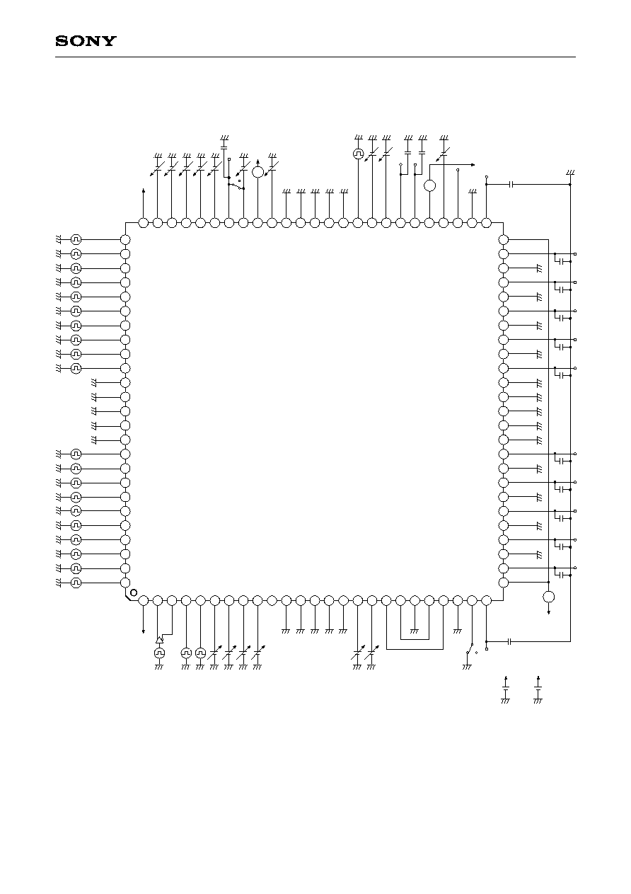
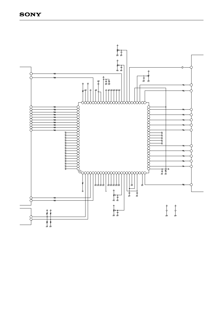
Block Diagram and Pin Configuration
1
2
3
4
5
6
7
8
9 10 11 12 13 14 15 16 17 18 19 20 21 22 23 24 25
26
27
28
29
30
31
32
33
34
35
36
37
38
39
40
41
42
43
44
45
46
47
48
49
50
51
52
53
54
55
56
57
58
59
60
61
62
63
64
65
66
67
68
69
70
71
72
73
74
75
76
77
78
79
80
81
82
83
84
85
86
87
88
89
90
91
92
93
94
95
96
97
98
99
100
D_A9
TEST
SL_INV
SL_SCN
SL_D
A
T
DIRC
F/H_CNT
VREF_O
VREF_I
V
DD
PS
GND
GND
GND
GND
GND
PRG
SID_L
V
PRG_L
V
SID_OUT
SID_OUTX
V
CC
VCOM_OFST
VCOM_OUT
NC
SH_OUT1
PV
CC
SH_OUT2
NC
SH_OUT3
NC
SH_OUT4
NC
SH_OUT5
NC
SH_OUT6
GND
D_A8
D_A7
D_A6
D_A5
D_A4
D_A3
D_A2
D_A1
D_A0
GND
GND
GND
GND
GND
D_B9
D_B8
D_B7
D_B6
D_B5
D_B4
D_B3
D_B2
D_B1
D_B0
GND
PGND
GND
GND
SH_OUT7
NC
NC
NC
NC
SH_OUT8
SH_OUT9
SH_OUT10
SH_OUT11
PV
CC
TEST
POSCTR0
MCLK
MCLKX
FRP
SHST
POSCTR1
POSCTR2
POSCTR3
SHTEST
GND
GND
GND
GND
GND
GND
DCFBOFF
NC
CAL_IL
CAL_IH
CAL_OH
CAL_OL
SIG_OFST
SIG.C
SH_OUT12
Line Inv.
VCOM Gen.
SID Gen.
Offset Cancel
Line Inv.
Offset Cancel
Line Inv.
Offset Cancel
Line Inv.
Offset Cancel
Line Inv.
Offset Cancel
Line Inv.
Offset Cancel
Line Inv.
S/H
D/A
Vref Gen.
Offset Cancel
Line Inv.
Offset Cancel
Line Inv.
Offset Cancel
Line Inv.
Offset Cancel
Line Inv.
Offset Cancel
Line Inv.
FRP_OD
FRP_EV
CAL_PLS
Offset Cancel
TG
Offset Cancel Level Gen.
S/H
S/H
S/H
S/H
S/H
S/H
S/H
S/H
S/H
S/H
S/H
S/H
S/H
S/H
S/H
S/H
S/H
S/H
S/H
S/H
S/H
S/H
S/H
S/H
S/H
S/H
S/H
S/H
S/H
S/H
S/H
S/H
S/H
S/H
S/H
D/A

≠ 3 ≠
CXA3562R
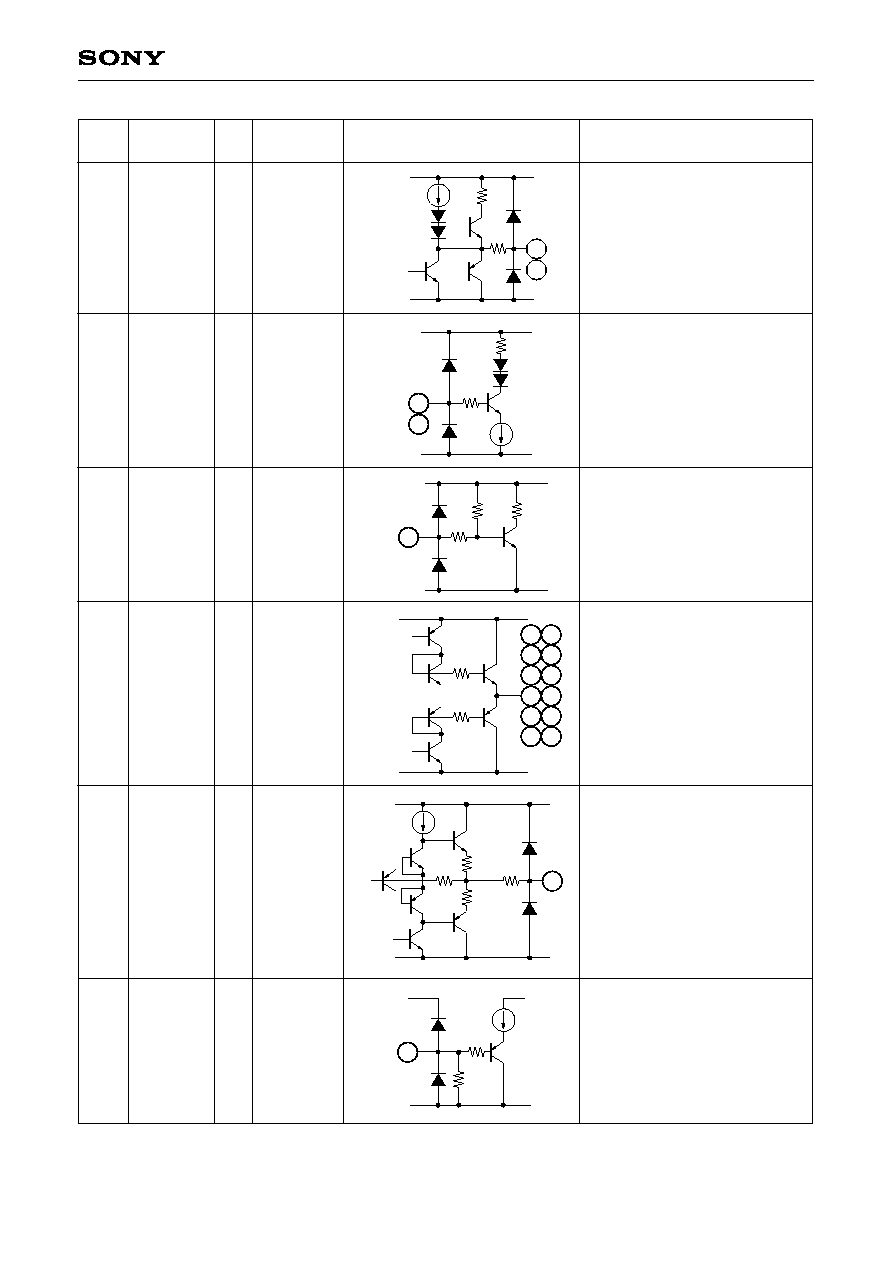
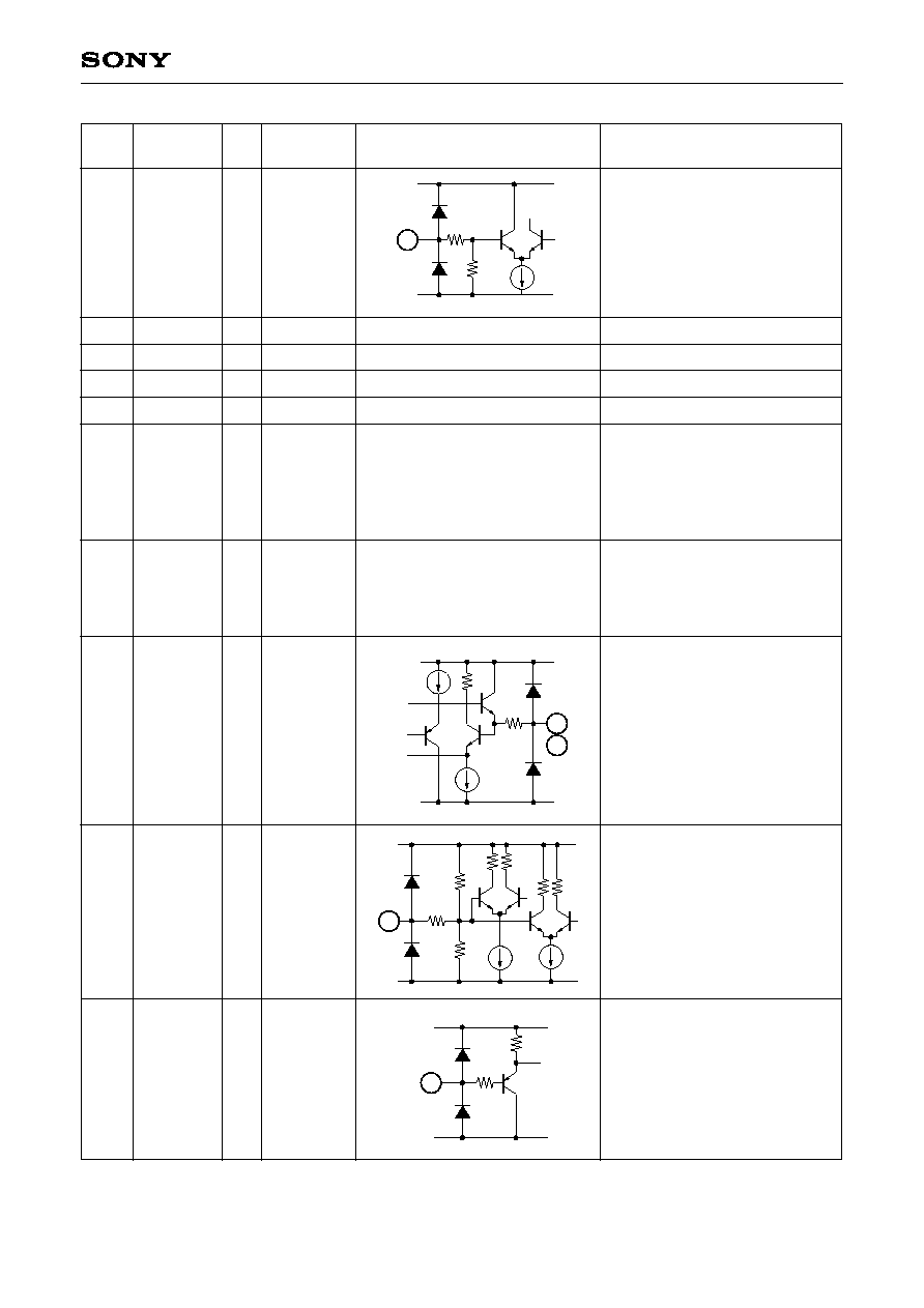
Pin Description
Pin
No.
Symbol
I/O
Standard
voltage level
Equivalent circuit
Description
V
DD
140k
60k
60k
100Ķ
1k
1k
140k
8k
GND
2
3
V
DD
GND
192
50k
4
PECL
differential
(amplitude
0.4V or more
between
V
DD
to 2V)
or TTL input
High:
2.0V
Low:
0.8V
High:
2.0V
Low:
0.8V
High:
2.0V
Low:
0.8V
V
DD
GND
192
50k
5
V
DD
GND
192
50k
9
8
7
6
V
DD
V
CC
GND
30k
20Ķ
16
V
DD
V
CC
GND
30k
10Ķ
17
1 to 5.0V
0 to 5.0V
I
SIG_OFST
17
I
SIG.C
16
I
POSCTR0
POSCTR1
POSCTR2
POSCTR3
6
7
8
9
I
SHST
5
I
FRP
4
I
MCLK
MCLKX
2
3
Dot clock input.
PECL differential input or TTL
input. For TTL input, input to
MCLK and connect MCLKX to
GND through a capacitor.
LCD panel AC drive inversion
timing input.
High: inverted
Low: non-inverted
See the Timing Chart.
Internal sample-and-hold timing
circuit reset pulse input.
This pin is also used as the
offset cancel level insertion
timing input.
A reset is applied to the internal
timing generator at the falling
edge.
Output phase adjustment.
The output phase is adjusted in
MCLK period units when
SL_DAT (Pin 72) is high, and in
1/2 MCLK period units when
SL_DAT is low.
Signal center voltage (inversion
folded voltage) adjustment input.
The SH_OUT output center
voltage can be adjusted in the
range from 7.0 to 8.0V.
Output signal offset adjustment
from signal center voltage.
The SH_OUT output 100%
white level (at 3FF input) voltage
can be adjusted in the range
from 0 to 1V from the center
voltage.
≠ 4 ≠
CXA3562R
3.0 to 6.0V
9.0 to 12.0V
9.0 to 12.0V
3.0 to 6.0V
GND
1.5 to 13.5V
5.0 to 8.0V
0 to 5.0V
I
VCOM_OFST
54
O
VCOM_OUT
53
O
SH_OUT12
to
SH_OUT1
25, 27,
29, 31,
33, 35,
41, 43,
45, 47,
49, 51
I
DCFBOFF
24
O
CAL_IH
CAL_IL
21
22
O
CAL_OL
CAL_OH
18
19
V
CC
GND
145
18
19
40Ķ
1k
20Ķ
V
CC
GND
30k
20k
21
22
V
DD
GND
145
24k
24
24k
PV
CC
GND
33
29
25
49
45
41
35
31
27
51
47
43
300
300
V
CC
GND
145
53
100k
80Ķ
500
500
V
DD
V
CC
GND
2k
100
80
Ķ
54
Pin
No.
Symbol
I/O
Standard
voltage level
Equivalent circuit
Description
Level output for canceling the
offset between channels.
Connect directly to CAL_IL and
CAL_IH, respectively.
Level input for canceling the
offset between channels.
Connect directly to CAL_OL and
CAL_OH, respectively. When
using two CXA3562R, connect
the CAL_IL and CAL_IH of both
chips to the CAL_OL and
CAL_OH of only one CXA3562R.
Offset cancel function off.
Normally connect to GND to
use with the offset cancel
function on.
High (offset cancel function off)
when open.
Demultiplexed output of AC
inverse driven video signals.
Can be connected directly to
the LCD panel.
LCD panel common voltage
output.
Can be set in the range from
the SH_OUT center potential
Vsig.c to Vsig.c ≠ 2V by
VCOM_OFST.
LCD panel common voltage
adjustment.
VCOM_OUT can be set in the
range from the SH_OUT center
potential Vsig.c to Vsig.c ≠ 2V
by inputting 0 to 5V.

≠ 5 ≠
CXA3562R
1.5 to 13.5V
1.0 to 5.0V
High:
2.0V
Low:
0.8V
3.2V
3.2V
High:
2.0V
Low:
0.8V
Open: Low
I
F/H_CNT
70
O
VREF_O
69
I
VREF_I
68
I
PRG
60
I
PRG_LV
SID_LV
58
59
O
SID_OUTX
SID_OUT
56
57
V
CC
GND
145
100k
56
57
100k
0.2p
0.2p
V
DD
V
CC
GND
50k
29Ķ
58
50k
59
V
DD
V
CC
GND
10k
60
100k
50
Ķ
V
DD
GND
1k
68
280Ķ
70Ķ
10Ķ
33.3k
V
DD
GND
69
20Ķ
2k
20k
12.4k
V
DD
GND
192
50k
70
200k
Pin
No.
Symbol
I/O
Standard
voltage level
Equivalent circuit
Description
Precharge waveform output.
SID_OUTX outputs the inverse
of SID_OUT based on the
output center voltage. These
pins cannot directly drive the
LCD panel, so input to the LCD
panel with an external a buffer.
Precharge level setting.
Adjusts the SID_OUT and
SID_OUTX output potential.
PRG_LV is reflected when the
PRG input pin (Pin 60) is high,
and SID_LV is reflected when
PRG is low.
Timing pulse input for switching
the Pins 56 and 57 output levels.
(See PRG_LV (Pin 58) and
SID_LV (Pin 59).)
Internal D/A converter reference
voltage input.
Normally connect directly to
VREF_O.
Reference voltage output.
Normally connect directly to
VREF_I, and connect to GND
through a 0.5 to 1.0ĶF capacitor.
SH_OUT output timing selection.
High: SH_OUT1 to SH_OUT6
and SH_OUT7 to SH_OUT12
are output at different timing.
Low: SH_OUT1 to SH_OUT12
are output at the same timing.
≠ 6 ≠
CXA3562R
Power GND.
Power V
CC
.
15V power supply.
5V power supply.
5V
1.7 to 3.2V
2.5V
High:
2.0V
Low:
0.8V
I
DIRC
71
I
SHTEST
10
O
TEST
1, 75
I
PS
66
V
DD
GND
70k
30Ķ
180k
66
V
DD
GND
192
1
75
1Ķ
20Ķ
2k
V
DD
GND
192
250k
20k
20k
10
250k
20k
20k
10Ķ
10Ķ
V
DD
GND
192
50k
71
GND
15.5V
15.5V
5V
GND
PGND
PV
CC
V
CC
V
DD
GND
NC
38
26, 50
55
67
11 to 15,
20, 36,
37, 39,
40,
61 to 65,
86 to 90
23, 28,
30, 32,
34, 42,
44, 46,
48, 52
Pin
No.
Symbol
I/O
Standard
voltage level
Equivalent circuit
Description
Power saving.
Power saving mode when set to
low level.
Low (power saving mode) when
open.
Normally connect to V
DD
.
GND.
DAC output monitor test.
Normally connect to V
DD
.
Test.
Leave open.
Scan direction setting.
High: output as a time series in
ascending order of output pin
symbol (in order from SH_OUT1
to SH_OUT12)
Low: output in descending order

≠ 7 ≠
CXA3562R
High:
2.0V
Low:
0.8V
Open: Low
High:
2.0V
Low:
0.8V
Open: High
High:
2.0V
Low:
0.8V
Open: Low
High:
2.0V
Low:
0.8V
High:
2.0V
Low:
0.8V
I
D_B9
to
D_B0
91
to
100
I
D_A9
to
D_A0
76
to
85
I
SL_INV
74
I
SL_SCN
73
I
SL_DAT
72
V
DD
GND
192
50k
72
200k
V
DD
GND
192
50k
73
200k
V
DD
GND
192
50k
74
200k
V
DD
GND
192
50k
85
76 to
V
DD
GND
192
50k
100
91 to
Pin
No.
Symbol
I/O
Standard
voltage level
Equivalent circuit
Description
Digital input mode switch setting.
High: single input from the A port
Low: parallel input from both the
A and B ports
A and B port input switching
interlocked/non-interlocked
setting relative to scan direction
setting during parallel input.
High: A and B port switching
interlocked to DIRC
Low: fixed regardless of DIRC
SH_OUT odd-numbered and
even-numbered output polarity
inverted/non-inverted setting.
High: odd-numbered and even-
numbered outputs inverted
Low: non-inverted
A port digital data input.
B port digital data input.
≠ 8 ≠
CXA3562R
Electrical Characteristics Measurement Circuit
1
2
3
4
5
6
7
8
9
10
11
12
13
14
15
16
17
18
19
20
21
22
23
24
25
26
27
28
29
30
31
32
33
34
35
36
37
38
39
40
41
42
43
44
45
46
47
48
49
50
51
52
53
54
55
56
57
58
59
60
61
62
63
64
65
66
67
68
69
70
71
72
73
74
75
76
77
78
79
80
81
82
83
84
85
86
87
88
89
90
91
92
93
94
95
96
97
98
99
100
D_A9
TEST
V
DD
SL_INV
SL_SCN
SL_D
A
T
DIRC
F/H_CNT
VREF_O
VREF_I
V
DD
PS
GND
GND
GND
GND
GND
PRG
SID_L
V
PRG_L
V
SID_OUT
SID_OUTX
V
CC
VCOM_OFST
VCOM_OUT
NC
SH_OUT1
PV
CC
SH_OUT2
NC
SH_OUT3
NC
SH_OUT4
NC
SH_OUT5
NC
SH_OUT6
GND
D_A8
D_A7
D_A6
D_A5
D_A4
D_A3
D_A2
D_A1
D_A0
GND
GND
GND
GND
GND
D_B9
D_B8
D_B7
D_B6
D_B5
D_B4
D_B3
D_B2
D_B1
D_B0
GND
PGND
GND
GND
SH_OUT7
NC
NC
NC
NC
SH_OUT8
SH_OUT9
SH_OUT10
SH_OUT11
PV
CC
V
CC
TEST
V
DD
POSCTR0
MCLK
MCLKX
FRP
SHST
POSCTR1
POSCTR2
POSCTR3
SHTEST
GND
GND
GND
GND
GND
GND
DCFBOFF
NC
CAL_IL
CAL_IH
CAL_OH
CAL_OL
SIG_OFST
SIG.C
SH_OUT12
360p
360p
360p
360p
360p
360p
360p
360p
360p
360p
360p
A
1Ķ
V
DD
A
47p
47p
360p
15.5V
V
CC
5V
V
DD
A
V
CC

≠ 9 ≠
CXA3562R
Electrical Characteristics
No.
Item
Symbol
Measurement
points
Measurement conditions
Min.
Typ. Max. Unit
1
2
3
4
5
6
7
8
9
10
11
12
13
14
15
Digital input
resolution
Digital input
setup time
Digital input
hold time
MCLK input
frequency
range 1
MCLK input
frequency
range 2
VREF_O output
voltage range
SH_OUT
amplitude 1
SH_OUT
amplitude 2
SH_OUT
minimum
amplitude
SH_OUT
slew rate
SH_OUT
minimum
output voltage
SH_OUT
maximum
output voltage
Output deviation
between
channels 1
Output deviation
between
channels 2
Output deviation
between ICs 1
n
T
S
T
H
f
MCLK1
f
MCLK2
V
VREF_O
V
SHOUT1p-p
V
SHOUT2p-p
V
OUTMINp-p
SR
OUT
V
MIN
V
MAX
D
OUT1
D
OUT2
D
IC1
V
OUT1
V
OUT2
V
OUT1
V
OUT1
to
V
OUT12
V
OUT1
to
V
OUT12
V
OUT1
to
V
OUT12
V
OUT1
to
V
OUT12
V
OUT1
to
V
OUT12
V
OUT1
to
V
OUT12
SHST, D_A[9:0] and D_B[9:0] minimum
setup time relative to MCLK input. (PELL)
SHST, D_A[9:0] and D_B[9:0] minimum
hold time relative to MCLK input. (PECL)
SL_DAT: 5V; maximum frequency at
which the internal timing generator
and D/A converter operate normally.
SL_DAT: 0V; maximum frequency at
which the internal timing generator
and D/A converter operate normally.
Measure the VREF_O (Pin 69)
voltage.
Measure the SH_OUT1 voltage
difference at D_A[9:0]: 000h and 3FFh.
Measure the SH_OUT2 voltage
difference at D_B[9:0]: 000h and 3FFh.
Lower the VREF_I voltage and adjust
the amplitude; minimum amplitude at
which SH_OUT1 can be output at
D_B[9:0]: 000h and 3FFh.
Load capacitance = 360pF; measure
slew rate at 10 to 90% of output
waveform rise and fall when D_A[9:0]
is varied from 000h to 3FFh and from
3FFh to 000h.
Minimum voltage at which sample-
and-hold outputs V
OUT1
to V
OUT12
can
be output.
Maximum voltage at which sample-
and-hold outputs V
OUT1
to V
OUT12
can
be output.
Value obtained by subtracting minimum
V
OUT1
to V
OUT12
value from maximum
V
OUT1
to V
OUT12
value at D_A[9:0]: 200h
and D_B[9:0]: 200h.
Value obtained by subtracting minimum
V
OUT1
to V
OUT12
value from maximum
V
OUT1
to V
OUT12
value at D_A[9:0]: 000h
or 3FFh and D_B[9:0]: 000h or 3FFh.
Value obtained by subtracting minimum
V
OUT1
to V
OUT12
value from maximum
V
OUT1
to V
OUT12
value at D_A[9:0]: 200h
and D_B[9:0]: 200h. (when using two
CXA3562R)
10
--
--
--
--
3.20
4.50
4.50
--
300
--
--
3
10
10
bit
ns
ns
MHz
MHz
V
V
V
V
V/Ķs
V
V
mVp-p
mVp-p
mVp-p
--
2
3
30
60
3.10
4.44
4.44
4
160
1.5
--
--
--
--
--
--
--
80
100
3.32
4.83
4.83
--
--
--
13.6
10
40
--

≠ 10 ≠
CXA3562R
16
17
18
19
20
21
22
23
24
25
26
27
Output deviation
between ICs 2
SID output
gain 1
SID output
gain 2
SID output
slew rate
Signal center
adjustable range
SH_OUT offset
adjustable range
VCOM
adjustable range
V
DD
current
consumption
V
CC
current
consumption
Current
consumption in
power saving
mode
Differential
linearity error
Integral linearity
error
D
IC2
A
SID1
A
SID2
SR
SID
V
SIG
V
SIGOFST
V
COM
I
DD
I
CC
I
PS
DLE
ILE
V
OUT1
to
V
OUT12
V
SID_LV
V
SID
V
SIDX
V
PRG_LV
V
SID
V
SIDX
V
SID
V
SIDX
V
OUT1
V
OUT1
V
COM
I
VDD
I
VCC1
I
VCC2
I
VDD
I
VCC1
I
VCC2
--
--
Value obtained by subtracting minimum
V
OUT1
to V
OUT12
value from maximum
V
OUT1
to V
OUT12
value at D_A[9:0]: 000h
or 3FFh and D_B[9:0]: 000h or 3FFh.
(when using two CXA3562R)
PRG: 0V; measure V
SID_LV
and V
SID
at
FRP: 0V, and V
SID_LV
and V
SIDX
at
FRP: 5V.
Calculate as A
SID1
= V
SID(X)
/V
SID_LV
.
PRG: 5V; measure V
PRG_LV
and V
SID
at
FRP: 0V, and V
PRG_LV
and V
SIDX
at
FRP: 5V.
Calculate as A
SID2
= V
SID(X)
/V
PRG_LV
.
Load capacitance = 47pF, PRG: 0V;
input a repeating high/low pulse to FRP
(Pin 4), and apply DC input voltage so
that V
SID
and V
SIDX
are 2.5V/11.5V.
Measure slew rate at 10 to 90% of
output waveform rise and fall.
V
OUT1
center voltage when SIG.C
(Pin 16) is varied from 1 to 5V.
D_A[9:0]: 3FFh, FRP: 0V, D_B[9:0]:
3FFh; value obtained by subtracting
V
OUT1
from V
OUT1
center voltage when
SIG_OFST (Pin 17) is varied from 1 to
5V.
VCOM_OUT voltage when VCOM_OFST
(Pin 54) is varied from 0 to 5V.
I
DD
= I
VDD
I
CC
= I
VCC1
+ I
VCC2
(no digital data input)
GND (Pin 66),
I
CC
= I
VDD
+ I
VCC1
+ I
VCC2
V
VREF
_I = 3.2V
V
VREF
_I = 3.2V
20
2.0
2.0
50
--
--
--
85
40
8
--
--
mVp-p
times
times
V/Ķs
V
V
V
mA
mA
mA
LSB
LSB
No.
Item
Symbol
Measurement
points
Measurement conditions
Min.
Typ.
Max. Unit
--
1.9
1.9
15
7
0
Vc ≠
2.5
59
21
4
≠0.7
≠1.2
--
2.1
2.1
--
8
1
Vc
112
59
15
0.7
1.2

≠ 11 ≠
CXA3562R
Description of Operation
The flow of internal operations is described below.
The digital signals input to D_A9 to D_A0 and D_B9 to D_B0 are internally D/A converted into approximately
1.5V (at VREF_I: 3.2V) analog signals. After that, the signal that has been demultiplexed into 12 phases is
amplified by a factor of three times, inverted at the signal center potential according to FRP, and output.
The output level relative to the digital input changes according to the following settings.
A: SIG_OFST voltage
B: VREF_I voltage
C: SIG.C voltage
1. Digital input block
The CXA3562R can be set to single input from only the A port or parallel input from both the A and B ports,
and port switching by right/left inversion is also possible in parallel input mode. This makes it possible to
support various systems.
In single input mode, the signal is internally demultiplexed to 2-parallel format and input to the D/A converter.
2. D/A converter block
The internal D/A converter has two systems for odd-numbered and even-numbered outputs. The voltage input
from VREF_I becomes the 100% white level potential of the analog converted signal, and this amplitude is a
maximum 1.5Vp-p with respect to input data of 000h to 3FFh.
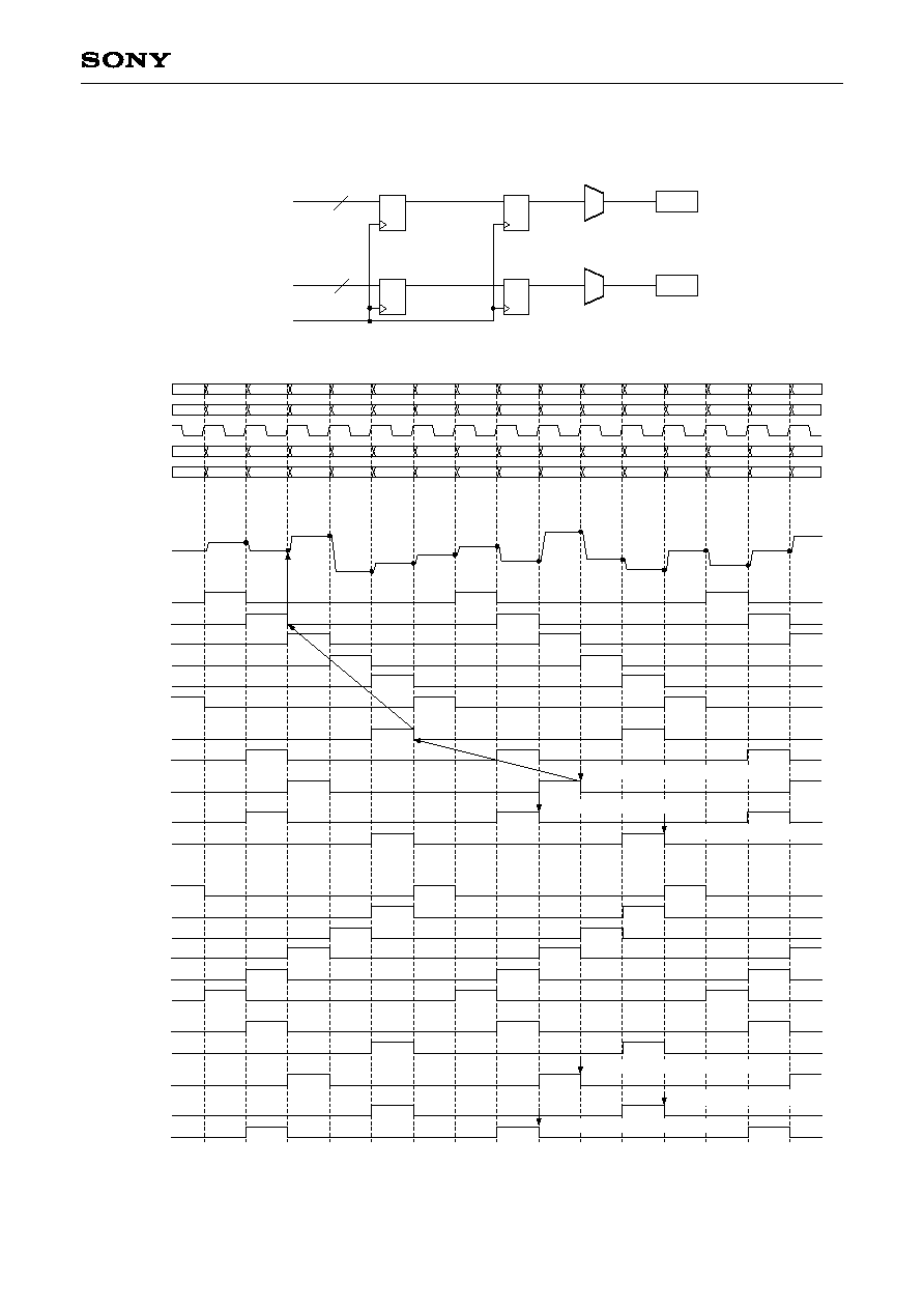
3. Sample-and-hold (S/H) block
The odd-numbered and even-numbered D/A converter outputs are input to the odd-numbered and even-
numbered sample-and-hold blocks, respectively. The signals are converted from time series signals into 6-phase
cyclic parallel signals by the sample-and-hold group which is appropriately controlled by the internal timing
generator. For forward scan, the signals are output in the ascending order of SH_OUT1, SH_OUT2, SH_OUT3
... SH_OUT12. For reverse scan, this order is inverted and the signals are output in descending order. Connect
the signals to the LCD panel according to the order used. The timing of each sample-and-hold pulse is shown
on the following pages. These pulses are not output and are used only inside the IC.
V
CC
GND
Signal Center
1023
512
0
A
A
B
B
C
Digital IN
SH_OUT

≠ 12 ≠
CXA3562R
Single input mode
D
D
DAC
DAC
S/H
S/H
D_A[9:0]
MCLK/2
D_A2
D_A1
D_B2
DAC_O
MCLK
D
10bit
D_A[9:0]
D_A1
D_A2
DAC_O
MCLK
D_B2
SH1_1_2
SH1_3_4
SH1_5_6
SH1_7_8
SH1_9_10
SH1_11_12
SH2_1_6
SH2_7_12
SH3A_1_12
SH3B_7_12
SH3B_1_6
SH1_1_2
SH1_3_4
SH1_5_6
SH1_7_8
SH1_9_10
SH1_11_12
SH2_1_6
SH2_7_12
SH3A_1_12
SH3B_7_12
SH3B_1_6
DIRC: H
DIRC: L
F/H_CNT: L
F/H_CNT: H
F/H_CNT: L
F/H_CNT: H
D
D
1
3
CH1 to CH12 simultaneous output timing
CH1 to CH6 simultaneous output timing
CH7 to CH12 simultaneous output timing
CH1 to CH12 simultaneous output timing
CH1 to CH6 simultaneous output timing
CH7 to CH12 simultaneous output timing
0
1
2
3
4
5
6
7
8
9
10 11 12 13 14 15 16 17 18 19 20 21 22 23 24 25 26 27 28 29
0
0
2
4
6
8
10
12
14
16
18
20
22
24
26
28
1
3
5
7
9
11
13
15
17
19
21
23
25
27
1
2
3
4
5
6
7
8
9
10 11 12 13 14 15 16 17 18 19 20 21 22 23 24 25 26 27 28 29
≠ 13 ≠
CXA3562R
2-parallel input mode
D
D
DAC
DAC
S/H
S/H
D_A[9:0]
MCLK
D_A2
D_B2
DAC_O
D_B[9:0]
D
10bit
D
10bit
1
3
D_A[9:0]
MCLK
D_A2
DAC_O
1
3
5
7
9
11
13
15
17
19
21
23
25
27
2
4
6
8
0
10
12
14
16
18
20
22
24
26
28
D_B[9:0]
2
4
6
8
0
10
12
14
16
18
20
22
24
26
D_B2
1
3
5
7
9
11
13
15
17
19
21
23
25
≠1
≠1
≠3
≠2
≠3
≠2
≠5
≠4
≠1
SH1_1_2
SH1_3_4
SH1_5_6
SH1_7_8
SH1_9_10
SH1_11_12
SH2_1_6
SH2_7_12
SH3A_1_12
SH3B_7_12
SH3B_1_6
SH1_1_2
SH1_3_4
SH1_5_6
SH1_7_8
SH1_9_10
SH1_11_12
SH2_1_6
SH2_7_12
SH3A_1_12
SH3B_7_12
SH3B_1_6
DIRC: H
DIRC: L
F/H_CNT: L
F/H_CNT : H
F/H_CNT: L
F/H_CNT: H
D
CH1 to CH12 simultaneous output timing
CH1 to CH6 simultaneous output timing
CH7 to CH12 simultaneous output timing
CH1 to CH12 simultaneous output timing
CH1 to CH6 simultaneous output timing
CH7 to CH12 simultaneous output timing

≠ 14 ≠
CXA3562R
4. Timing generator (TG) block
The internal timing generator operates by one pair of differential clock inputs (MCLK, MCLKX) and a horizontal sync
signal input (SHST), and generates the timing pulses needed by the demultiplexer block, dot inversion control pulse
and output deviation cancel circuit. The various operating modes can be designated by the pin settings.
The SHST and FRP inputs should satisfy the relationship shown in the figure below with the MCLK and
MCLKX input period as 1clk.
The CXA3562R can select various operating modes according to the timing generator block settings. These
settings are described below.
∑ SL_DAT (Pin 72)
Digital input selection. Single input from only the A port is selected when set to high level, and parallel input
from both the A and B ports is selected when set to low level. When inputting a 2-parallel processed digital
video signal in parallel input mode, input the earlier time series data to the A port and the later time series data
to the B port. Input a master clock having the same period as the input data rate to MCLK in both modes.
This pin is low level (2-parallel input mode) when left open.
∑ DIRC (Pin 71), SL_SCN (Pin 73)
Scan direction settings. Output is ascending order when DIRC is set to high level, and inverted to descending
order (SH_OUT1 to SH_OUT12) when set to low level. At this time if SL_SCN is set to high, the A and B port
data can be switched by switching DIRC between high and low. When SL_SCN is set to low, the A port data is
output from the odd-numbered SH_OUT and the B port data is output from the even-numbered SH_OUT
regardless of the DIRC setting.
Set SL_SCN to high when SL_DAT is high.
SL_SCN: L
SL_SCN: H
SH_OUT1: A6, SH_OUT2: B6,
SH_OUT3: A5, SH_OUT4: B5,
SH_OUT5: A4, SH_OUT6: B4,
SH_OUT7: A3, SH_OUT8: B3,
SH_OUT9: A2, SH_OUT10: B2,
SH_OUT11: A1, SH_OUT12: B1
SH_OUT1: B6, SH_OUT2: A6,
SH_OUT3: B5, SH_OUT4: A5,
SH_OUT5: B4, SH_OUT6: A4,
SH_OUT7: B3, SH_OUT8: A3,
SH_OUT9: B2, SH_OUT10: A2,
SH_OUT11: B1, SH_OUT12: A1
SH_OUT1: A1, SH_OUT2: B1,
SH_OUT3: A2, SH_OUT4: B2,
SH_OUT5: A3, SH_OUT6: B3,
SH_OUT7: A4, SH_OUT8: B4,
SH_OUT9: A5, SH_OUT10: B5,
SH_OUT11: A6, SH_OUT12: B6
SH_OUT1: A1, SH_OUT2: B1,
SH_OUT3: A2, SH_OUT4: B2,
SH_OUT5: A3, SH_OUT6: B3,
SH_OUT7: A4, SH_OUT8: B4,
SH_OUT9: A5, SH_OUT10: B5,
SH_OUT11: A6, SH_OUT12: B6
DIRC: H
DIRC: L
30clk or more
1Ķs or more
SHST
FRP
A1
A2
A3
A4
A5
A6
B1
B2
B3
B4
B5
B6
D_A[9:0]
D_B[9:0]

≠ 15 ≠
CXA3562R
∑ SL_INV (Pin 74)
Dot inversion and line inversion selection. When set to low level, all SH_OUT channels are output at the same
polarity as shown by the solid line in the figure below. When set to high level, the odd-numbered and even-
numbered SH_OUT outputs are output at inverse polarities. At this time the odd-numbered outputs are
inverted when the FRP pulse is high, and non-inverted when the FRP pulse is low. Conversely, the even-
numbered outputs are inverted when the FRP pulse is low, and non-inverted when the FRP pulse is high.
∑ Output phase setting
The phase of each SH_OUT output can be adjusted in MCLK period units when SL_DAT is high or in 1/2 MCLK
period units when SL_DAT is low by POSCTR[3:0] (Pins 6 to 9). The phase can be set in 16 ways by 4-bit digital
input. The output phase shifts backward by the above unit each time this setting is increased by one bit.
∑ F/H_CNT (Pin 70)
SH_OUT output timing phase setting. When set to low level, all SH_OUT outputs are output at the same
timing. When set to high level, SH_OUT1 to SH_OUT6 and SH_OUT7 to SH_OUT12 are output at phases
offset by 1/2 clock period from each other.
SH_OUT
GND
FRP
GND
SH_OUT1 to 6
SH_OUT7 to 12
GND
SH_OUT1 to 6
SH_OUT7 to 12
F/H_CNT: L
F/H_CNT: H

≠ 16 ≠
CXA3562R
5. Calibration level generator block
The CXA3562R generates the offset cancel circuit reference with a calibration level generator in order to
minimize the deviation between channels at the center level.
The 200h output level is generated at both the AC output high and low sides, and these levels are DC output
from CAL_OH and CAL_OL, respectively. At the same time, 200h data is forcibly inserted into the video signal
while the video blanking period SHST pulse is low level, and feedback is applied so that the output levels of all
SH_OUT channels conform to CAL_IH and CAL_IL during this period.
6. SID signal generator block
This circuit generates the precharge signal waveform used by the LCD panel.
The voltage input from PRG_LV (Pin 58) and SID_LV (Pin 59) is switched by the PRG pulse (Pin 60). The
PRG_LV voltage is selected when PRG is high, and the SID_LV voltage is selected when PRG is low. This
signal is then further amplified by a factor of two times and folded by the FRP pulse. The folded center voltage
is the SH_OUT center voltage (voltage set by the SIG.C pin). SID_OUT (Pin 57) is inverted when FRP is high,
and non-inverted when FRP is low. Conversely, SID_OUTX (Pin 56) is inverted when FRP is low, and non-
inverted when FRP is high.
SID_OUT and SID_OUTX cannot directly drive the precharge signal input of the LCD panel, so they should be
connected via a buffer having sufficient current supply capability.
7. VCOM potential generator block
This block sets the DC common potential for the LCD panel.
VCOM_OFST (Pin 54) sets the deviation relative to the SH_OUT center potential, which is set by SIG.C.
SHST
FRP
SH_OUT
200h
200h
000h
000h
CAL_PLS
(internal pulse)
200ns
Video signal replacement period
Signal center
Offset cancel operation
Delayed by sample-and-hold

≠ 17 ≠
CXA3562R
Example of Representative Characteristics (V
CC
= 15.5V, V
DD
= 5.0V, Ta = 25įC)
VREF_I voltage vs. SH_OUT voltage white-black amplitude
3.2
3.1
3.0
2.9
2.8
2.7
4.6
4.5
4.3
4.2
4.4
4.1
4.0
3.9
3.8
4.8
4.7
SH_OUT white-b
lac
k amplitude v
oltage [V]
VREF_I voltage [V]
Input data vs. SH_OUT voltage
3FFh
300h
200h
100h
000h
12
10
8
6
0
14
SH_OUT v
oltage [V]
Input data (10 bits)
4
2
SIG.C voltage vs. SH_OUT center voltage
4.0
3.5
3.0
2.5
8.0
8.5
7.0
6.0
5.0
5.5
7.5
SH_OUT center v
oltage [V]
SIG.C voltage [V]
SIG_OFST voltage vs. SH_OUT voltage
5.0
2.0
2.5
3.0
3.5
4.0
4.5
1.5
1.0
0.5
11
10
9
8
6
7
3
12
SH_OUT v
oltage [V]
SIG_OFST voltage [V]
5
4
VCOM_OFST voltage vs. VCOM_OUT voltage
3.1
3.0
2.9
2.8
5.95
5.85
5.80
5.70
6.00
VCOM_OUT v
oltage [V]
VCOM_OFST voltage [V]
3.3
4.5
6.5
9.0
3.2
5.90
5.75
<Measurement conditions>
SIG.C = 3.75V
SIG_OFST = 3.6V
<Measurement conditions>
SIG_OFST = 3.6V
<Measurement conditions>
SIG.C = 3.75V
<Measurement conditions>
SIG.C = 3.75V
SIG_OFST = 3.6V
<Measurement conditions>
SIG.C = 3.75V
DATA = 200h
FRP = High
FRP = Low
FRP = High
FRP = Low

≠ 18 ≠
CXA3562R
12
10
8
6
0
14
16
4
2
PRG_LV voltage vs. SID_OUT voltage
4
3
2
1
0
SID_OUT v
oltage [V]
FRP = High
FRP = Low
SID_LV voltage vs. SID_OUT voltage
4
3
2
PRG_LV voltage [V]
SID_LV voltage [V]
1
0
12
10
8
6
0
14
16
SID_OUT v
oltage [V]
4
2
<Measurement conditions>
SIG.C = 3.75V
<Measurement conditions>
SIG.C = 3.75V
FRP = High
FRP = Low
≠ 19 ≠
CXA3562R
Application Circuit 1 (to XGA Panel)
1
2
3
4
5
6
7
8
9 10 11 12 13 14 15 16 17 18 19 20 21 22 23 24 25
26
27
28
29
30
31
32
33
34
35
36
37
38
39
40
41
42
43
44
45
46
47
48
49
50
51
52
53
54
55
56
57
58
59
60
61
62
63
64
65
66
67
68
69
70
71
72
73
74
75
76
77
78
79
80
81
82
83
84
85
86
87
88
89
90
91
92
93
94
95
96
97
98
99
100
V
DD
V
DD
V
DD
V
DD
V
DD
V
DD
47ĶF
20k
1ĶF
0.1ĶF
0.1ĶF
10k
10
R1OUT9
RGT
PRG
DSD
CXD3511Q
R1OUT8
R1OUT7
R1OUT6
R1OUT5
R1OUT4
R1OUT3
R1OUT2
R1OUT1
R1OUT0
FRP
SHST
CLKH
CXA3266Q
CLKL
D_A9
TEST
SL_INV
SL_SCN
SL_D
A
T
DIRC
F/H_CNT
VREF_O
VREF_I
V
DD
PS
GND
GND
GND
GND
GND
PRG
SID_L
V
PRG_L
V
SID_OUT
SID_OUTX
V
CC
VCOM_OFST
VCOM_OUT
NC
SH_OUT1
PV
CC
SH_OUT2
NC
SH_OUT3
NC
SH_OUT4
NC
SH_OUT5
NC
SH_OUT6
GND
1
10
10
10
D_A8
10
D_A7
10
D_A6
10
D_A5
10
D_A4
10
D_A3
10
D_A2
10
D_A1
10
D_A0
10
10
82
GND
GND
CXA3562R
GND
GND
GND
D_B9
D_B8
D_B7
D_B6
D_B5
D_B4
D_B3
D_B2
D_B1
D_B0
V
DD
20k
0.1ĶF
V
DD
20k
GND
PGND
GND
GND
1
1
1
1
SH_OUT7
NC
NC
NC
NC
1
SH_OUT8
1
SH_OUT9
1
SH_OUT10
1
SH_OUT11
PV
CC
1
V
CC
47ĶF
0.1ĶF
10k
TEST
POSCTR0
MCLK
MCLKX
FRP
SHST
POSCTR1
POSCTR2
POSCTR3
SHTEST
OPEN
GND
GND
GND
GND
GND
GND
DCFBOFF
NC
CAL_IL
CAL_IH
CAL_OH
CAL_OL
SIG_OFST
SIG.C
SH_OUT12
V
DD
V
DD
20k
0.1ĶF
1ĶF
1ĶF
V
DD
20k
0.1ĶF
V
CC
15.5V
121
122
111
112
113
116
117
118
119
120
157
159
130
82
130
V
DD
1
Vsig12
Vsig11
Vsig10
Vsig9
Vsig8
Vsig7
Vsig6
LCD Panel
LCX023
Vsig5
Vsig4
Vsig3
Vsig2
1
Vsig1
5V
Buffer
Psig
1
136
161
31
32
14
11
12
13
9
10
4
5
6
7
8
1
COM
3
31
Application circuits shown are typical examples illustrating the operation of the devices. Sony cannot assume responsibility for
any problems arising out of the use of these circuits or for any infringement of third party patent and other right due to same.
≠ 20 ≠
CXA3562R
Application Circuit 2 (to SXGA Panel)
1
2
3
4
5
6
7
8
9 10 11 12 13 14 15 16 17 18 19 20 21 22 23 24 25
26
27
28
29
30
31
32
33
34
35
36
37
38
39
40
41
42
43
44
45
46
47
48
49
50
51
52
53
54
55
56
57
58
59
60
61
62
63
64
65
66
67
68
69
70
71
72
73
74
75
76
77
78
79
80
81
82
83
84
85
86
87
88
89
90
91
92
93
94
95
96
97
98
99
100
V
DD
V
DD
V
DD
V
DD
V
DD
47ĶF
20k
1ĶF
0.1ĶF
0.1ĶF
10k
10
R1OUT9
RGT
PRG
DSD
CXD3511Q
R1OUT8
R1OUT7
R1OUT6
R1OUT5
R1OUT4
R1OUT3
R1OUT2
R1OUT1
R1OUT0
FRP
SHST
CLK/2H
CXA3266Q
CLK/2L
D_A9
TEST
SL_INV
SL_SCN
SL_D
A
T
DIRC
F/H_CNT
VREF_O
VREF_I
V
DD
PS
GND
GND
GND
GND
GND
PRG
SID_L
V
PRG_L
V
SID_OUT
SID_OUTX
V
CC
VCOM_OFST
VCOM_OUT
NC
SH_OUT1
PV
CC
SH_OUT2
NC
SH_OUT3
NC
SH_OUT4
NC
SH_OUT5
NC
SH_OUT6
GND
1
10
10
10
D_A8
10
D_A7
10
D_A6
10
D_A5
10
D_A4
10
D_A3
10
D_A2
10
D_A1
10
D_A0
R2OUT9
10
R2OUT8
10
R2OUT7
10
R2OUT6
10
R2OUT5
10
R2OUT4
10
R2OUT3
10
R2OUT2
10
R2OUT1
10
R2OUT0
10
10
10
82
GND
GND
CXA3562R
GND
GND
GND
D_B9
D_B8
D_B7
D_B6
D_B5
D_B4
D_B3
D_B2
D_B1
D_B0
V
DD
20k
0.1ĶF
V
DD
20k
GND
PGND
GND
GND
1
1
1
1
SH_OUT7
NC
NC
NC
NC
1
SH_OUT8
1
SH_OUT9
1
SH_OUT10
1
SH_OUT11
PV
CC
1
V
CC
47ĶF
0.1ĶF
10k
TEST
POSCTR0
MCLK
MCLKX
FRP
SHST
POSCTR1
POSCTR2
POSCTR3
SHTEST
OPEN
GND
GND
GND
GND
GND
GND
DCFBOFF
NC
CAL_IL
CAL_IH
CAL_OH
CAL_OL
SIG_OFST
SIG.C
SH_OUT12
V
DD
V
DD
20k
0.1ĶF
1ĶF
1ĶF
V
DD
20k
0.1ĶF
V
CC
15.5V
121
122
111
112
113
116
117
118
119
120
157
159
130
82
130
V
DD
1
Vsig12
Vsig11
Vsig10
Vsig9
Vsig8
Vsig7
Vsig6
LCD Panel
LCX028
Vsig5
Vsig4
Vsig3
Vsig2
1
Vsig1
5V
Buffer
Psig
1
136
161
14
11
12
13
9
10
4
5
6
7
8
1
COM
COML
COMR
3
2
21
32
103
104
105
106
107
108
109
110
98
99
29
30
Application circuits shown are typical examples illustrating the operation of the devices. Sony cannot assume responsibility for
any problems arising out of the use of these circuits or for any infringement of third party patent and other right due to same.
≠ 21 ≠
CXA3562R
Application Circuit 3 (to WXGA Panel)
1
2
3
4
5
6
7
8
9 10 11 12 13 14 15 16 17 18 19 20 21 22 23 24 25
26
27
28
29
30
31
32
33
34
35
36
37
38
39
40
41
42
43
44
45
46
47
48
49
50
51
52
53
54
55
56
57
58
59
60
61
62
63
64
65
66
67
68
69
70
71
72
73
74
75
76
77
78
79
80
81
82
83
84
85
86
87
88
89
90
91
92
93
94
95
96
97
98
99
100
V
DD
V
DD
V
DD
V
DD
V
DD
V
DD
V
DD
47ĶF
20k
1ĶF
0.1ĶF
10k
10
R1OUT9
RGT
DSD
CXD3511Q
R1OUT8
R1OUT7
R1OUT6
R1OUT5
R1OUT4
R1OUT3
R1OUT2
R1OUT1
R1OUT0
FRP
SHST
CLK/2H
CXA3266Q
CLK/2L
D_A9
TEST
SL_INV
SL_SCN
SL_D
A
T
DIRC
F/H_CNT
VREF_O
VREF_I
V
DD
PS
GND
GND
GND
GND
GND
PRG
SID_L
V
PRG_L
V
SID_OUT
SID_OUTX
V
CC
VCOM_OFST
VCOM_OUT
NC
SH_OUT1
PV
CC
SH_OUT2
NC
SH_OUT3
NC
SH_OUT4
NC
SH_OUT5
NC
SH_OUT6
GND
1
10
10
D_A8
10
D_A7
10
D_A6
10
D_A5
10
D_A4
10
D_A3
10
D_A2
10
D_A1
10
D_A0
R2OUT9
10
R2OUT8
10
R2OUT7
10
R2OUT6
10
R2OUT5
10
R2OUT4
10
R2OUT3
10
R2OUT2
10
R2OUT1
10
R2OUT0
10
10
10
82
GND
GND
CXA3562R
GND
GND
GND
D_B9
D_B8
D_B7
D_B6
D_B5
D_B4
D_B3
D_B2
D_B1
D_B0
V
DD
20k
0.1ĶF
GND
PGND
GND
GND
1
1
1
1
SH_OUT7
NC
NC
NC
NC
1
SH_OUT8
1
SH_OUT9
1
SH_OUT10
1
SH_OUT11
PV
CC
1
V
CC
47ĶF
0.1ĶF
10k
TEST
POSCTR0
MCLK
MCLKX
FRP
SHST
POSCTR1
POSCTR2
POSCTR3
SHTEST
OPEN
GND
GND
GND
GND
GND
GND
DCFBOFF
NC
CAL_IL
CAL_IH
CAL_OH
CAL_OL
SIG_OFST
SIG.C
SH_OUT12
V
DD
V
DD
20k
0.1ĶF
1ĶF
1ĶF
V
DD
20k
0.1ĶF
V
CC
15.5V
121
122
111
112
113
116
117
118
119
120
157
159
130
82
130
V
DD
1
Vsig-b6
Vsig-b5
Vsig-b4
Vsig-b3
Vsig-b2
Vsig-b1
Vsig-a6
LCD Panel
LCX037
Vsig-a5
Vsig-a4
Vsig-a3
Vsig-a2
1
Vsig-a1
5V
Buffer
Another
CXA3562R
SID_OUTX
SID_OUT
Psig1
Psig2
Psig3
Psig4
136
1
COM
COML
COMR
103
104
105
106
107
108
109
110
98
99
29
30
2
3
4
5
56
57
8
9
10
11
12
13
14
15
16
17
18
6
25
34
7
Application circuits shown are typical examples illustrating the operation of the devices. Sony cannot assume responsibility for
any problems arising out of the use of these circuits or for any infringement of third party patent and other right due to same.

≠ 22 ≠
CXA3562R
Application Circuit 4 (to UXGA Panel)
1
2
3
4
5
6
7
8
9 10 11 12 13 14 15 16 17 18 19 20 21 22 23 24 25
26
27
28
29
30
31
32
33
34
35
36
37
38
39
40
41
42
43
44
45
46
47
48
49
50
51
52
53
54
55
56
57
58
59
60
61
62
63
64
65
66
67
68
69
70
71
72
73
74
75
76
77
78
79
80
81
82
83
84
85
86
87
88
89
90
91
92
93
94
95
96
97
98
99
100
V
DD
V
DD
V
DD
V
DD
V
DD
V
DD
47ĶF
0.47ĶF
0.1ĶF
10k
10
R1OUT9
RGT
DSD
CXD3511Q
R1OUT8
R1OUT7
R1OUT6
R1OUT5
R1OUT4
R1OUT3
R1OUT2
R1OUT1
R1OUT0
FRP
SHST
R2OUT9
R2OUT8
R2OUT7
R2OUT6
R2OUT5
R2OUT4
R2OUT3
R2OUT2
R2OUT1
R2OUT0
XFRP
CLK/2H
CXA3266Q
CLK/2L
D_A9
TEST
SL_INV
SL_SCN
SL_D
A
T
DIRC
F/H_CNT
VREF_O
VREF_I
V
DD
PS
GND
GND
GND
GND
GND
SID_OUT
SID_OUTX
V
CC
VCOM_OFST
VCOM_OUT
NC
SH_OUT1
PV
CC
SH_OUT2
NC
SH_OUT3
NC
SH_OUT4
NC
SH_OUT5
NC
SH_OUT6
GND
1
10
10
D_A8
10
D_A7
10
D_A6
10
D_A5
10
D_A4
10
D_A3
10
D_A2
10
D_A1
10
D_A0
10
10
82
GND
GND
CXA3562R
CXA3562R
GND
GND
GND
D_B9
D_B8
D_B7
D_B6
D_B5
D_B4
D_B3
D_B2
D_B1
D_B0
GND
PGND
GND
GND
1
1
1
1
SH_OUT7
NC
NC
NC
NC
1
SH_OUT8
1
SH_OUT9
1
SH_OUT10
1
SH_OUT11
PV
CC
1
V
CC
47ĶF
0.1ĶF
10k
TEST
POSCTR0
MCLK
MCLKX
FRP
SHST
POSCTR1
POSCTR2
POSCTR3
SHTEST
OPEN
GND
GND
GND
GND
GND
GND
DCFBOFF
NC
CAL_IL
CAL_IH
CAL_OH
CAL_OL
SIG_OFST
SIG.C
SH_OUT12
V
DD
V
DD
OPEN
V
DD
20k
0.1ĶF
0.47ĶF
0.47ĶF
1
2
3
4
5
6
7
8
9 10 11 12 13 14 15 16 17 18 19 20 21 22 23 24 25
26
27
28
29
30
31
32
33
34
35
36
37
38
39
40
41
42
43
44
45
46
47
48
49
50
51
52
53
54
55
56
57
58
59
60
61
62
63
64
65
66
67
68
69
70
71
72
73
74
75
76
77
78
79
80
81
82
83
84
85
86
87
88
89
90
91
92
93
94
95
96
97
98
99
100
V
DD
V
DD
V
DD
V
DD
V
DD
V
DD
47ĶF
20k
0.47ĶF
0.1ĶF
0.1ĶF
10k
10
D_A9
TEST
SL_INV
SL_SCN
SL_D
A
T
DIRC
F/H_CNT
VREF_O
VREF_I
V
DD
PS
GND
GND
GND
GND
GND
PRG
SID_L
V
PRG_L
V
SID_OUT
SID_OUTX
V
CC
VCOM_OFST
VCOM_OUT
NC
SH_OUT1
PV
CC
SH_OUT2
NC
SH_OUT3
NC
SH_OUT4
NC
SH_OUT5
NC
SH_OUT6
GND
10
D_A8
10
D_A7
10
D_A6
10
D_A5
10
D_A4
10
D_A3
10
D_A2
10
D_A1
10
D_A0
10
GND
GND
GND
GND
GND
D_B9
D_B8
D_B7
D_B6
D_B5
D_B4
D_B3
D_B2
D_B1
D_B0
V
DD
20k
0.1ĶF
GND
PGND
GND
GND
SH_OUT7
NC
NC
NC
NC
SH_OUT8
SH_OUT9
SH_OUT10
SH_OUT11
PV
CC
V
CC
47ĶF
0.1ĶF
10k
TEST
POSCTR0
MCLK
MCLKX
FRP
SHST
POSCTR1
POSCTR2
POSCTR3
SHTEST
GND
GND
GND
GND
GND
GND
DCFBOFF
NC
CAL_IL
CAL_IH
CAL_OH
CAL_OL
SIG_OFST
SIG.C
SH_OUT12
V
DD
20k
0.1ĶF
V
CC
15.5V
0.1ĶF
0.47ĶF
0.47ĶF
1
Buffer
1
1
1
1
1
1
1
1
1
1
1
1
121
122
111
112
113
116
117
118
119
120
98
99
103
104
105
106
107
108
109
110
157
159
130
82
130
158
29
30
V
DD
Sig24
Sig22
Sig20
Sig18
Sig16
Sig14
Sig12
Sig10
Sig8
Sig6
Sig4
VSig2
COM2
1
Vsig23
Vsig21
Vsig19
Vsig17
Vsig15
Vsig13
Vsig11
LCD Panel
LCX036
Vsig9
Vsig7
Vsig5
Vsig3
1
Vsig1
COM1
Psig3
Psig4
5V
34
24
26
28
30
32
14
16
18
20
22
12
56
57
Buffer
Psig1
Psig2
3
4
33
23
25
27
29
31
21
13
15
17
19
11
1
2
136
V
DD
20k
0.1ĶF
SID_L
V
PRG_L
V
V
DD
20k
PRG
PRG
10
161
0.1ĶF
Application circuits shown are typical examples illustrating the operation of the devices. Sony cannot assume responsibility for
any problems arising out of the use of these circuits or for any infringement of third party patent and other right due to same.

≠ 23 ≠
CXA3562R
Notes on Operation
The CXA3562R has high power consumption, so be sure to take the following radiation measures.
∑ Use four-layer substrate.
∑ GND lines connected between Pins 11 to 15, Pins 36 to 40, Pins 61 to 65 and Pins 86 to 90 should be as
thick as possible.

≠ 24 ≠
CXA3562R
100PIN LQFP (PLASTIC)
25
26
51
50
75
76
1
100
SONY CODE
EIAJ CODE
JEDEC CODE
PACKAGE MATERIAL
LEAD TREATMENT
LEAD MATERIAL
PACKAGE MASS
EPOXY RESIN
PALLADIUM PLATING
COPPER ALLOY
PACKAGE STRUCTURE
DETAIL A
LQFP-100P-L01
P-LQFP100-14x14-0.5
16.0 Ī 0.2
14.0 Ī 0.1
0.5
b
(0.22)
A
1.5 ≠ 0.1
+ 0.2
0.5 Ī
0.2
(15.0)
0į to 10į
0.1 Ī 0.1
0.5 Ī
0.2
0.1
NOTE: Dimension "
" does not include mold protrusion.
0.7g
0.13 M
b = 0.18 Ī 0.03
0.125 Ī
0.04
DETAIL B : PALLADIUM
B
Sony Corporation
Package Outline Unit: mm