 | –≠–ª–µ–∫—Ç—Ä–æ–Ω–Ω—ã–π –∫–æ–º–ø–æ–Ω–µ–Ω—Ç: CXA3627N | –°–∫–∞—á–∞—Ç—å:  PDF PDF  ZIP ZIP |

≠ 1 ≠
E02715A2Y-PS
Sony reserves the right to change products and specifications without prior notice. This information does not convey any license by
any implication or otherwise under any patents or other right. Application circuits shown, if any, are typical examples illustrating the
operation of the devices. Sony cannot assume responsibility for any problems arising out of the use of these circuits.
CXA3627N
30 pin SSOP (Plastic)
Description
The CXA3627N is a monolithic TV tuner IC which
integrates local oscillator and mixer circuits for VHF
band, local oscillator and mixer circuits for UHF
band, an IF amplifier and a tuning PLL onto a single
chip, enabling further miniaturization of the tuner.
Features
∑ Low power consumption (5V, 63mA typ.)
∑ Low noise figure, low distortion characteristics
∑ High gain/low gain selectable
∑ Supports IF double-tuned/adjacent channel trap
∑ Balanced oscillator circuits with excellent oscillation
stability
∑ On-chip PLL supports I
2
C bus
∑ On-chip high voltage drive transistor for charge
pump
∑ Frequency step selectable from 31.25, 50 or
62.5kHz (when using a 4MHz crystal)
∑ Low-phase noise synthesizer
∑ On-chip 4-output band switch (output voltage: 5V,
current capacity: 13mA)
∑ 30-pin SSOP small package
∑ UHF band switch output switchable
Applications
∑ TV tuners
∑ VCR tuners
∑ CATV tuners
Structure
Bipolar silicon monolithic IC
All Band Tuner IC with On-chip PLL
Absolute Maximum Ratings
∑ Supply voltage
V
CC
≠0.3 to +5.5
V
∑ Operating temperature
Topr
≠25 to +75
∞C
∑ Storage temperature
Tstg
≠55 to +150
∞C
∑ Allowable power dissipation
P
D
580
mW
Operating Conditions
Supply voltage
V
CC
4.75 to 5.30
V
Note: This IC has pins whose electrostatic discharge strength is weak as the operating frequency is high
and the high-frequency process is used for this IC. Take care of handling the IC.
≠ 2 ≠
CXA3627N
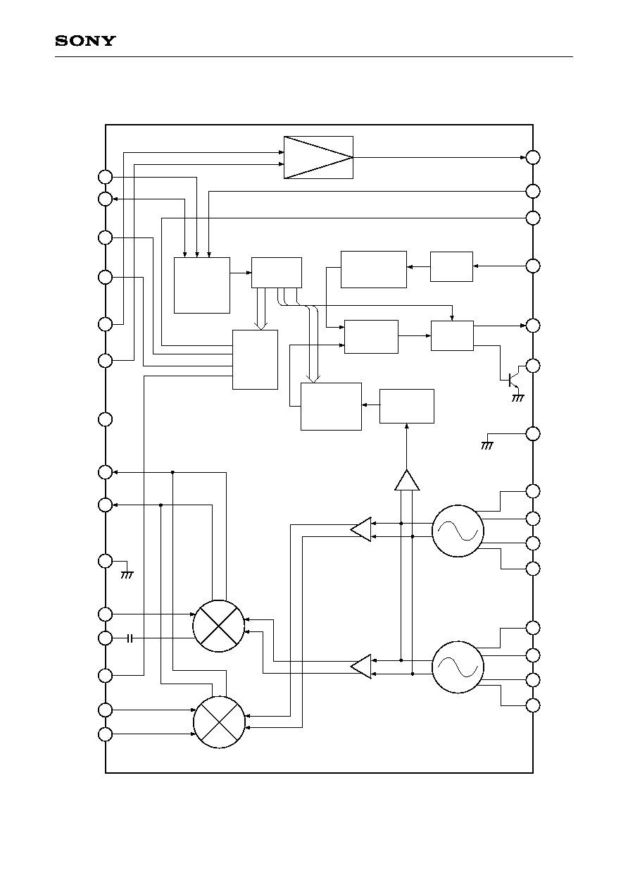
Block Diagram and Pin Configuration
1
2
3
4
5
6
7
8
9
10
11
12
13
14
15
30
29
28
27
26
25
24
23
22
21
20
IF AMP
I
2
C Bus
Interface
Shift
Register
Divider
1/128, 160, 256
Charge
Pump
REF
OSC
Phase
Detector
Band SW
Driver
Programmable
Divider
14/15 bit
Prescaler
1/2
VHF
MIX
UHF
MIX
SCL
SDA
BS1
BS2
IFIN1
IFIN2
Vcc
MIXOUT1
MIXOUT2
GND1
VHFIN
BYP
BS4
UHFIN1
UHFIN2
UOSCB1
UOSCE1
UOSCE2
UOSCB2
19
18
17
16 VOSCB1
VOSCC1
VOSCC2
VOSCB2
GND2
VT
CPO
REF
OSC
BS3
ADSW
IFOUT
≠ 3 ≠
CXA3627N
Pin Description
Pin
No.
1
2
3
4
5
6
7
8
9
10
11
12
13
14
15
16
17
18
19
20
21
22
23
24
25
26
27
28
29
30
Symbol
SCL
SDA
BS1
BS2
IFIN1
IFIN2
Vcc
MIXOUT1
MIXOUT2
GND1
VHFIN
BYP
BS4
UHFIN1
UHFIN2
VOSCB1
VOSCC1
VOSCC2
VOSCB2
UOSCB1
UOSCE1
UOSCE2
UOSCB2
GND2
VT
CPO
REFOSC
BS3
ADSW
IFOUT
Description
SCL input
SDA I/O
Band switch output 1
Band switch output 2
IF amplifier input
IF amplifier input
Power supply
MIX output (open collector)
MIX output (open collector)
Analog circuit GND
VHF input
Switch of VHF input GND and UHF band switch output
(GND: UHF for BS4, Open: UHF for BS3)
Band switch output 4
UHF input
UHF input
VHF oscillator (base pin)
VHF oscillator (collector pin)
VHF oscillator (collector pin)
VHF oscillator (base pin)
UHF oscillator (base pin)
UHF oscillator (emitter pin)
UHF oscillator (emitter pin)
UHF oscillator (base pin)
PLL circuit GND
Tuning voltage output (open collector)
Charge pump output (loop filter connection)
Crystal connection for PLL reference oscillator
Band switch output 3
Address selection (I
2
C bus)
IF amplifier output
≠ 4 ≠
CXA3627N
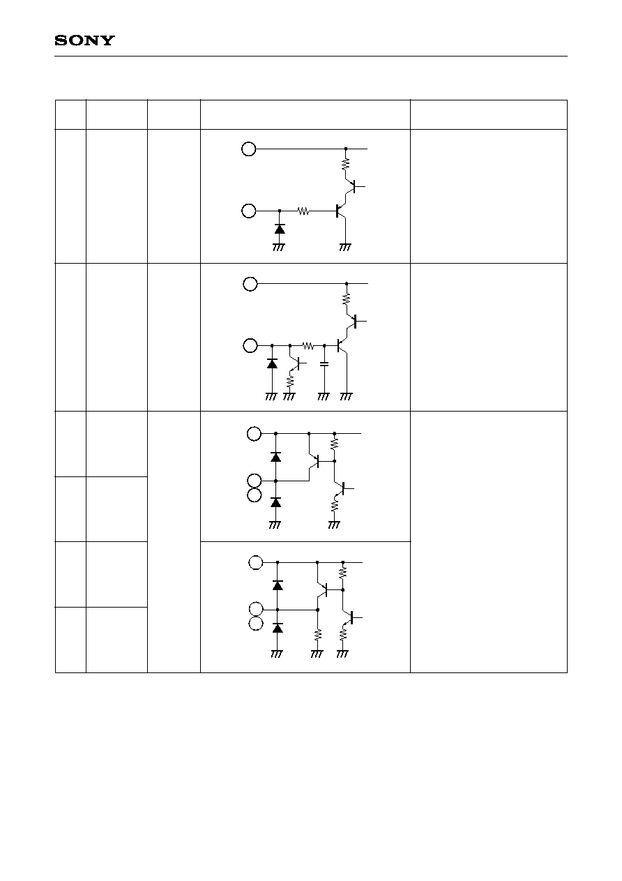
Pin Description
1
7
40k
40k
5p
2
7
7
3
4
100k
7
13
14
Pin
No.
Symbol
Pin voltage
[V]
Equivalent circuit
Description
1
SCL
--
Clock input
2
SDA
--
Data input
3
BS1
4
BS2
High: 4.9
Low: 0.0
Band switch outputs.
This pin corresponding to the
selected band goes High.
13
BS4
28
BS3
≠ 5 ≠
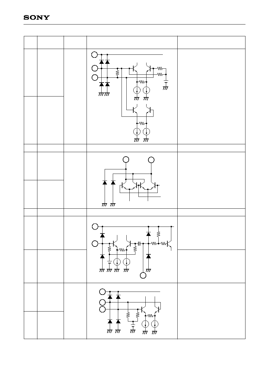
CXA3627N
Pin
No.
Symbol
Pin voltage
[V]
Equivalent circuit
Description
7
5
6
1.6k
8
9
7
11
12
3k
3k
15p
100
10k
7
14
15
3k
3k
5
IFIN1
6
IFIN2
2.0
IF inputs.
These pins must be connected
to the mixer outputs via
coupling capacitance.
7
V
CC
--
Power supply.
8
MIXOUT1
9
MIXOUT2
--
Mixer outputs.
These pins output the signal in
open collector format, and they
must be connected to the
power supply via a load.
11
VHFIN
2.4 during
VHF reception
0.0 during
UHF reception
VHF input.
The input format is unbalanced
input.
12
BYP
3.8
(when open)
VHF input GND and selection
of band switching.
GND: BS4 UHF
Open: BS3 UHF
14
UHFIN1
15
UHFIN2
UHF inputs.
Input a balanced signal to
Pins 14 and 15, or ground
either of Pin 14 or 15 with a
capacitor and input the signal
to the other pin.
10
GND1
--
Analog circuit GND.
0.0 during
VHF reception
2.3 during
UHF reception
≠ 6 ≠
CXA3627N
Pin
No.
Symbol
Pin voltage
[V]
Equivalent circuit
Description
7
20
20
19
16
5k
5k
18
17
3k
3k
21
22
23
20
7
7
25
26
70
16
VOSCB1
2.3 during
VHF reception
2.5 during
UHF reception
18
VOSCC1
4.0 during
VHF reception
5.0 during
UHF reception
17
VOSCC2
4.0 during
VHF reception
5.0 during
UHF reception
19
VOSCB2
2.3 during
VHF reception
2.5 during
UHF reception
External resonance circuit
connection for VHF oscillator.
20
UOSCB1
2.4 during
VHF reception
2.2 during
UHF reception
21
UOSCE1
2.0 during
VHF reception
1.5 during
UHF reception
22
UOSCE2
2.0 during
VHF reception
1.5 during
UHF reception
23
UOSCB2
2.4 during
VHF reception
2.2 during
UHF reception
External resonance circuit
connection for UHF oscillator.
25p
38p
30k
100
7
27
24
GND2
--
PLL circuit GND.
25
VT
--
Varicap drive voltage output.
This pin outputs the signal in
open collector format, and it
must be connected to the
tuning power supply via a load.
26
CPO
2.0
Charge pump output.
Connects the loop filter.
27
REFOSC
4.4
Crystal connection for
reference oscillator.
--

≠ 7 ≠
CXA3627N
Pin
No.
Symbol
Pin voltage
[V]
Equivalent circuit
Description
150k
50k
5p
29
7
7
30
29
ADSW
1.25
(when open)
Address selection.
Controls address bits 1 and 2.
30
IFOUT
2.8
IF output.
≠ 8 ≠
CXA3627N
Electrical Characteristics (See the Electrical Characteristics Measurement Circuit.)
(Vcc = 5V, IFV
CC
= 5V, Ta = 25∞C)
Circuit Current
Item
Symbol
Iccv
Iccu
Measurement conditions
V
CC
current
Band switch output open during VHF operation
V
CC
current
Band switch output open during UHF operation
Min.
Typ.
64
63
Max.
Unit
mA
mA
OSC/MIX/IF Amplifier Block
Item
Symbol
CG1
CG2
CG3
CG4
CG5
CG6
CG7
CG8
NF1
NF2
NF3
NF4
NF5
NF6
NF7
NF8
CM1
CM2
CM3
CM4
CM5
CM6
CM7
CM8
Pomax
Measurement conditions
VHF operation f
RF
= 55MHz
High gain mode
VHF operation f
RF
= 360MHz High gain mode
UHF operation f
RF
= 360MHz High gain mode
UHF operation f
RF
= 800MHz High gain mode
VHF operation f
RF
= 55MHz
Low gain mode
VHF operation f
RF
= 360MHz Low gain mode
UHF operation f
RF
= 360MHz Low gain mode
UHF operation f
RF
= 800MHz Low gain mode
VHF operation f
RF
= 55MHz
High gain mode
VHF operation f
RF
= 360MHz High gain mode
UHF operation f
RF
= 360MHz High gain mode
UHF operation f
RF
= 800MHz High gain mode
VHF operation f
RF
= 55MHz
Low gain mode
VHF operation f
RF
= 360MHz Low gain mode
UHF operation f
RF
= 360MHz Low gain mode
UHF operation f
RF
= 800MHz Low gain mode
VHF operation f
D
= 55MHz
f
UD
= ±12MHz (30% AM)
High gain mode
VHF operation f
D
= 360MHz
f
UD
= ±12MHz (30% AM)
High gain mode
UHF operation f
D
= 360MHz
f
UD
= ±12MHz (30% AM)
High gain mode
UHF operation f
D
= 800MHz
f
UD
= ±12MHz (30% AM)
High gain mode
VHF operation f
D
= 55MHz
f
UD
= ±12MHz (30% AM)
Low gain mode
VHF operation f
D
= 360MHz
f
UD
= ±12MHz (30% AM)
Low gain mode
UHF operation f
D
= 360MHz
f
UD
= ±12MHz (30% AM)
Low gain mode
UHF operation f
D
= 800MHz
f
UD
= ±12MHz (30% AM)
Low gain mode
50
load, saturation output
Min.
Typ.
22.0
22.5
26.0
26.0
20.0
20.5
24.0
24.0
12
12
10
11
13
13
11
12
103
103
101
98
104
104
102
98
11
Max.
Unit
dB
dB
dB
dB
dB
dB
dB
dB
dB
dB
dB
dB
dB
dB
dB
dB
dBµ
dBµ
dBµ
dBµ
dBµ
dBµ
dBµ
dBµ
dBm
88
87
41
40
25.0
25.5
29.0
29.0
23.0
23.5
27.0
27.0
15
15
13
14
16
16
14
15
19.0
19.5
23.0
23.0
17.0
17.5
21.0
21.0
99
99
97
94
100
100
98
94
8
Circuit current
Conversion gain
1
Noise figure
1
,
2
1% cross
modulation 1
1
,
3
Maximum output power
≠ 9 ≠
CXA3627N
Item
Symbol
fsw1
fsw2
fsw3
fsw4
fst1
fst2
fst3
fst4
C/N1
C/N2
Measurement conditions
VHF operation
f
OSC
= 100MHz
f from 3s to 3min after switch ON
VHF operation
f
OSC
= 405MHz
f from 3s to 3min after switch ON
UHF operation
f
OSC
= 405MHz
f from 3s to 3min after switch ON
UHF operation
f
OSC
= 845MHz
f from 3s to 3min after switch ON
VHF operation
f
OSC
= 100MHz
f when V
CC
5V changes ±5%
VHF operation
f
OSC
= 405MHz
f when V
CC
5V changes ±5%
UHF operation
f
OSC
= 405MHz
f when V
CC
5V changes ±5%
UHF operation
f
OSC
= 845MHz
f when V
CC
5V changes ±5%
VHF operation
10kHz offset CP = 1
Phase comparison frequency = 31.25kHz
UHF operation
10kHz offset CP = 1
Phase comparison frequency = 31.25kHz
Min.
Typ.
80
80
Max.
Unit
kHz
kHz
kHz
kHz
kHz
kHz
kHz
kHz
dBc/Hz
dBc/Hz
±200
±650
±350
±400
±100
±350
±100
±100
1
Value measured with untuned input.
2
NF meter direct-reading value (DSB measurement).
3
Value with a desired reception signal input level of ≠30dBm, an interference signal of 100kHz/30% AM,
and an interference signal level where S/I = 46dB measured with a spectrum analyzer.
4
Value when the PLL is not operating.
Switch ON drift
(PLL not
operating)
4
Supply voltage drift
(PLL not
operating)
4
Oscillator phase
noise
≠ 10 ≠
CXA3627N
PLL Block
Item
Lock-up time
Reference leak
CL and DA inputs
"H" level input voltage
"L" level input voltage
"H" level input current
"L" level input current
AD input
"H" level input voltage
"L" level input voltage
"H" level input current
"L" level input current
SDA output
"H" output leak current
"L" output voltage
CPO (charge pump)
Output current 1
Leak current 1
Output current 2
Leak current 2
VT (VC voltage output)
Maximum output voltage
Minimum output voltage
REFOSC
Oscillation frequency range
Input capacitance
Negative resistance
Band SW
Output current
Saturation voltage
Leak current
Symbol
LUT1
LUT2
REFL
V
IH
V
IL
I
IH
I
IL
V
IH
V
IL
I
IH
I
IL
I
SDALK
V
SDAL
I
CPO1
LeakCP1
I
CPO2
LeakCP2
V
TH
V
TL
F
XTOSC
C
XTOSC
R
NEG
I
BS
V
SAT
LeakBS
Measurement conditions
VHF operation
CP = 1
f
OSC
100MHz
f
OSC
405MHz
UHF operation
CP = 1
f
OSC
405MHz
f
OSC
845MHz
Phase comparison frequency
= 31.25kHz
CP = 1
V
IH
= Vcc
V
IL
= GND
V
IH
= Vcc
V
IL
= GND
V
IN
= 5.5V
Sink = ≠3mA
When CP = 0 is selected
When CP = 0 is selected
When CP = 1 is selected
When CP = 1 is selected
Sink current = 1mA
Crystal source impedance
f
REF
= 4MHz
When ON
When ON Source current =
13mA
When OFF IFV
CC
= 5.5V
Min.
Typ.
0
≠0.2
100
≠35
±50
±200
0.15
24
≠3
250
0.5
Max.
Unit
ms
ms
dBc
V
V
µA
µA
V
V
µA
µA
µA
V
µA
nA
µA
nA
V
V
MHz
pF
k
mA
mV
µA
50
50
Vcc
1.5
≠0.1
≠4
Vcc
1
200
≠100
5
0.4
±80
30
±320
100
34
0.8
12
26
≠13
330
3
50
3
GND
3
GND
GND
±30
±120
3
22
≠1
≠ 11 ≠
CXA3627N
Item
Bus timing (I
2
C bus)
SCL clock frequency
Start waiting time
Start hold time
Low hold time
High hold time
Start setup time
Data hold time
Data setup time
Rise time
Fall time
Stop setup time
Symbol
f
SCL
t
W;STA
t
H;STA
t
LOW
t
HIGH
t
S;STA
t
H;DAT
t
S;DAT
t
R
t
F
t
S;STO
Measurement conditions
Min.
Typ.
Max.
Unit
kHz
ns
ns
ns
ns
ns
ns
ns
ns
ns
ns
400
900
300
300
0
1300
600
1300
600
600
0
600
600

≠ 12 ≠
CXA3627N
Electrical Characteristics Measurement Circuit
30
IFOUT
29
ADSW
28
BS3
27
REFOSC
26
CPO
25
VT
24
GND2
23
UOSCB2
22
UOSCE2
21
UOSCE1
20
UOSCB1
19
V
OSCB2
18
V
OSCC2
17
V
OSCC1
16
1
2
3
4
5
6
7
8
9
10
11
12
13
14
15
V
OSCB1
SCL
SD
A
BS1
BS2
IFIN1
IFIN2
Vcc
MIXOUT1
MIXOUT2
GND1
VHFIN
BYP
BS4
UHFIN1
UHFIN2
51
ADSW
SCL
SDA
+5V
VHF IN
UHF IN
4.5T
4.5T
150p
150p
56p
56p
100
1n
1n
1n
360
1n
1n
1n
1n
4.7µ
51
360
360
BS2
1n
360
XTAL
4MHz
100p
220n
IF OUT
+30V
4700p
22k
10k
1T363
3.0
5.5T
2.5
2.5T
0.5p
1n
100p
1n
27
4.7k
15p
8p
2.2n
1n
4.7k
1k
10k
240
0.056µ
BS1
1T362
BS1
BS2
10k
2.5
2.5T
0.5p
1T363
10k
7p
1T363
0.5p
56p
7p
2p
7p
56p
4.7k
≠ 13 ≠
CXA3627N
Application Circuit
30
IFOUT
29
ADSW
28
BS3
27
REFOSC
26
CPO
25
VT
24
GND2
23
UOSCB2
22
UOSCE2
21
UOSCE1
20
UOSCB1
19
V
OSCB2
18
V
OSCC2
17
V
OSCC1
16
1
2
3
4
5
6
7
8
9
10
11
12
13
14
15
V
OSCB1
SCL
SD
A
BS1
BS2
IFIN1
IFIN2
Vcc
MIXOUT1
MIXOUT2
GND1
VHFIN
BYP
BS4
UHFIN1
UHFIN2
ADSW
SCL
SDA
+5V
VHF IN
UHF IN
4.5T
4.5T
1n
1n
56p
56p
1n
100
2k
1n
150p
3.2
7.5T
1n
1n
47p
47p
1n
1n
1n
4.7µ
BVL
BVH
200
200
3k
10p
1.2µH
XTAL
4MHz
100p
FMT
IF OUT
+30V
4700p
220n
22k
10k
2.5
1.5T
10k
0.5p
1T369
12p
100p
22p
8p
8p
100p
10k
240
0.056µ
1n
33p
3.8
14.5T
BU
1T363
3.0
5.5T
2.5
2.5T
0.5p
1n
100p
1n
27
4.7k
15p
8p
2.2n
1n
4.7k
1k
1T362
BS1
BS2
4.7k
BS2
BS1
Application circuits shown are typical examples illustrating the operation of the devices. Sony cannot assume responsibility for
any problems arising out of the use of these circuits or for any infringement of third party patent and other right due to same.
≠ 14 ≠
CXA3627N
Description of Functions
The CXA3627N is the terrestrial TV broadcasting tuner IC which converts frequencies to IF in order to tune
and detect only the desired reception frequency of VHF and UHF band signals.
In addition to the mixer, local oscillation and IF amplifier circuits required for frequency conversion to IF, this IC
also integrates a PLL circuit for local oscillation frequency control onto a single chip.
The functions of the various circuits are described below.
1. Mixer circuit
This circuit outputs the frequency difference between the signal input to VHFIN or UHFIN and the local
oscillation signal.
2. Local oscillation circuit
A VCO is formed by externally connecting an LC resonance circuit composed of a varicap diode and inductance.
3. IF amplifier circuit
This circuit amplifies the mixer IF output, and consists of an amplifier stage and low impedance output stage.
4. PLL circuit
This PLL circuit fixes the local oscillation frequency to the desired frequency. It consists of a programmable
divider, reference divider, phase comparator, charge pump and reference oscillator. The control format
supports the I
2
C bus format.
The frequency steps of 31.25, 50 or 62.5kHz can be selected by the I
2
C bus data-based reference divider
frequency division setting value.
5. Band switch circuit
The CXA3555N has four sets of built-in PNP transistors for switching between the VL, VH and UHF bands
and for switching the FM trap, etc. These PNP transistors can be controlled by the bus data.
The emitters for these PNP transistors are connected to the power supply pin (V
CC
), and are ON and output
5V when the bus data is "1 (H)".
Two types of relations of the bus data and the IC internal OSC/MIX circuits operation are available as shown
below. These relations can be selected by grounding or leaving open Pin 12 (BYP).
BYP: Grounding
: Don't care O: Operating X: Not operating
Band SW data
BS1
MIX circuit
OSC circuit
BS2
BS3
BS4
0
1
VHF
O
X
UHF
X
O
VHF
O
X
UHF
X
O
BYP: Open
Band SW data
BS1
MIX circuit
OSC circuit
BS2
BS3
0
1
BS4
VHF
O
X
UHF
X
O
VHF
O
X
UHF
X
O

≠ 15 ≠
CXA3627N
Description of Analog Block Operation (See the Electrical Characteristics Measurement Circuit.)
VHF oscillator circuit
∑ This is the differential amplifier-type oscillator circuit. Pins 16 and 19 are base and Pins 17 and 18 are
collector. Pins 16, 18 and Pins 19, 17 have the in-phase input/output relation respectively.
This circuit is oscillated with the positive feedback applied by connecting the output to the input via the
coupling capacitor and the feedback capacitor.
Oscillation frequency is varied by connecting an LC parallel resonance circuit including a varicap and controlling
the voltage applied to the varicap.
VHF mixer circuit
∑ The mixer circuit employs a double balanced mixer with little local oscillation signal leakage.
The input format is base input type, with Pin 12 grounded either directly or via a capacitor and the RF signal
input to Pin 11.
(Pin 12 can also be used to select VHF/UHF switching mode with the BS3/BS4 data.)
∑ The RF signal is fed from the oscillator, converted to IF frequency and output from Pins 8 and 9. Pins 8 and
9 are open collectors, so external power feed is necessary. Also, connect single-tuned filters to Pins 8 and 9.
UHF oscillator circuit
∑ The oscillator circuit is designed so that two collector ground type Colpitts oscillators perform differential
oscillation operation via an LC resonance circuit including a varicap.
∑ Resonance capacitance is connected between Pins 20 and 21, Pins 21 and 22, and Pins 22 and 23, and an
LC resonance circuit including a varicap is connected between Pins 20 and 23.
UHF mixer circuit
∑ This circuit employs a double balanced mixer like the VHF mixer circuit.
The input format is base input type, with Pins 14 and 15 as the RF input pins. The input method can be
selected from balanced input consisting of differential input to Pins 14 and 15 or unbalanced input consisting
of grounding Pin 14 via a capacitor and input to Pin 15.
∑ Pins 8 and 9 are the mixer outputs. Pins 8 and 9 are open collectors, so external power feed is necessary.
Also, connect single-tuned filters to Pins 8 and 9.
IF amplifier circuit
∑ Pins 5 and 6 are the IF amplifier inputs, and the input impedance is approximately 1.6k
.
∑ The signals frequency converted by the mixer are output from Pins 8 and 9, and Pins 8 and 9 are connected
to Pins 5 and 6 via capacitors. (An adjacent channel trap circuit can be formed by connecting LC parallel
circuits in place of capacitors.)
∑ The signal amplified by the IF amplifier is output from Pin 30. The output impedance is approximately 10
.
≠ 16 ≠
CXA3627N
Description of PLL Block
This IC is controlled by the I
2
C bus.
The PLL of this IC performs high-speed phase comparison, providing low reference leak and quick lock-up
time characteristics.
During power on, the power-on reset circuit operates to initialize the frequency data to all "0" and the band
data to all "OFF". Power-on reset is performed when V
CC
3.2V at room temperature (Ta = 25∞C).
1) Address setting
Up to four addresses can be selected by the hardware bit settings, so that multiple PLL can exist within one
system.
The responding address can be set according to the ADSW pin voltage.
Address
1
1
0
0
0
MA1
MA0
R/W
MA1
0
0
1
1
MA0
0
1
0
1
ADSW pin voltage
0 to 0.1Vcc
OPEN or
0.2Vcc to 0.3Vcc
0.4Vcc to 0.6Vcc
0.9Vcc to Vcc
Hardware bits
2) Frequency data setting
The VCO lock frequency is obtained according to the following formula.
fosc = 2
◊
fref
◊
(32M + S)
fosc: local oscillator frequency
fref: phase comparison frequency
M:
main divider frequency division ratio
S:
swallow counter frequency division ratio
The variable frequency division ranges of M and S are as follows, and are set as binary.
S < M
1023
0
S
31
≠ 17 ≠
CXA3627N
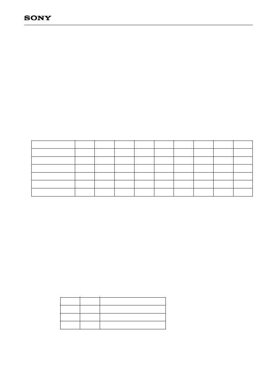
3) Control format
When performing control for this IC, byte 1 contains the address data, bytes 2 and 3 contain the frequency
data, byte 4 contains the control data, and byte 5 contains the band switch data.
These data are latch transferred in the manner of byte 1, byte 2 + byte 3, and byte 4 + byte 5.
When the correct address is received and acknowledged, the data is recognized as frequency data if the
first bit of the next byte is "0", and as control data and band switch data if this bit is "1".
Also, when data transmission is stopped part-way, the previously programmed data is valid. Therefore, once
the control and band switch data have been programmed, 3-byte commands consisting of the address and
frequency data are possible.
Further, even if the I
2
C bus stop conditions are not met, data can be input by sending the start conditions
and the new address.
The control format is as shown in the table below.
Slave Receiver
X: Don't care
A:
Acknowledge bit
MA0, MA1:
address setting
M0 to:
main divider frequency division ratio setting
S0 to:
swallow counter frequency division ratio setting
CD:
charge pump OFF (when "1")
OS:
varicap output OFF (when "1")
CP:
charge pump current switching (200µA when "1", 50µA when "0")
GC:
gain switching (IC gain reduced by 2dB when "1")
BS1 to BS4: band switch control (output PNP transistor ON when "1")
R0, R1:
reference divider frequency division ratio setting (See the Reference Divider Frequency Division
Ratio Table.)
Reference Divider Frequency Division Ratio Table
MSB
bit 7
1
0
M2
1
X
bit 6
1
M9
M1
CP
X
bit 5
0
M8
M0
GC
X
bit 4
0
M7
S4
CD
X
bit 3
0
M6
S3
X
BS4
bit 2
MA1
M5
S2
R1
BS3
bit 1
MA0
M4
S1
R0
BS2
LSB
bit 0
0
M3
S0
OS
BS1
A
A
A
A
A
Address byte
Divider byte1
Divider byte2
Control byte
Band SW byte
Mode
X: Don't care
R1
0
1
X
R0
1
1
0
Reference Divider
256
128
160
≠ 18 ≠
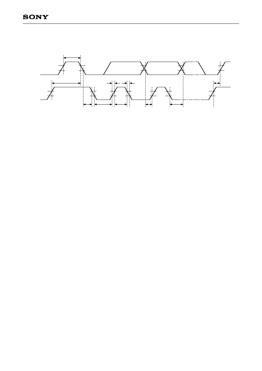
CXA3627N
SDA
t
W;STA
t
S;STA
t
H;STA
t
LOW
t
HIGH
t
S;DAT
t
H;DAT
t
S;STO
t
R
t
F
SCL
START
t
S;STA
= Start setup time
t
W;STA
= Start waiting time
t
H;STA
= Start hold time
t
LOW
= Low clock pulse width
t
HIGH
= High clock pulse width
t
S;DAT
= Data setup time
t
H;DAT
= Data hold time
t
S;STO
= Stop setup time
t
R
= Rise time
t
F
= Fall time
CLOCK
DATA CHANGE
STOP
I
2
C Bus Timing Chart
≠ 19 ≠
CXA3627N
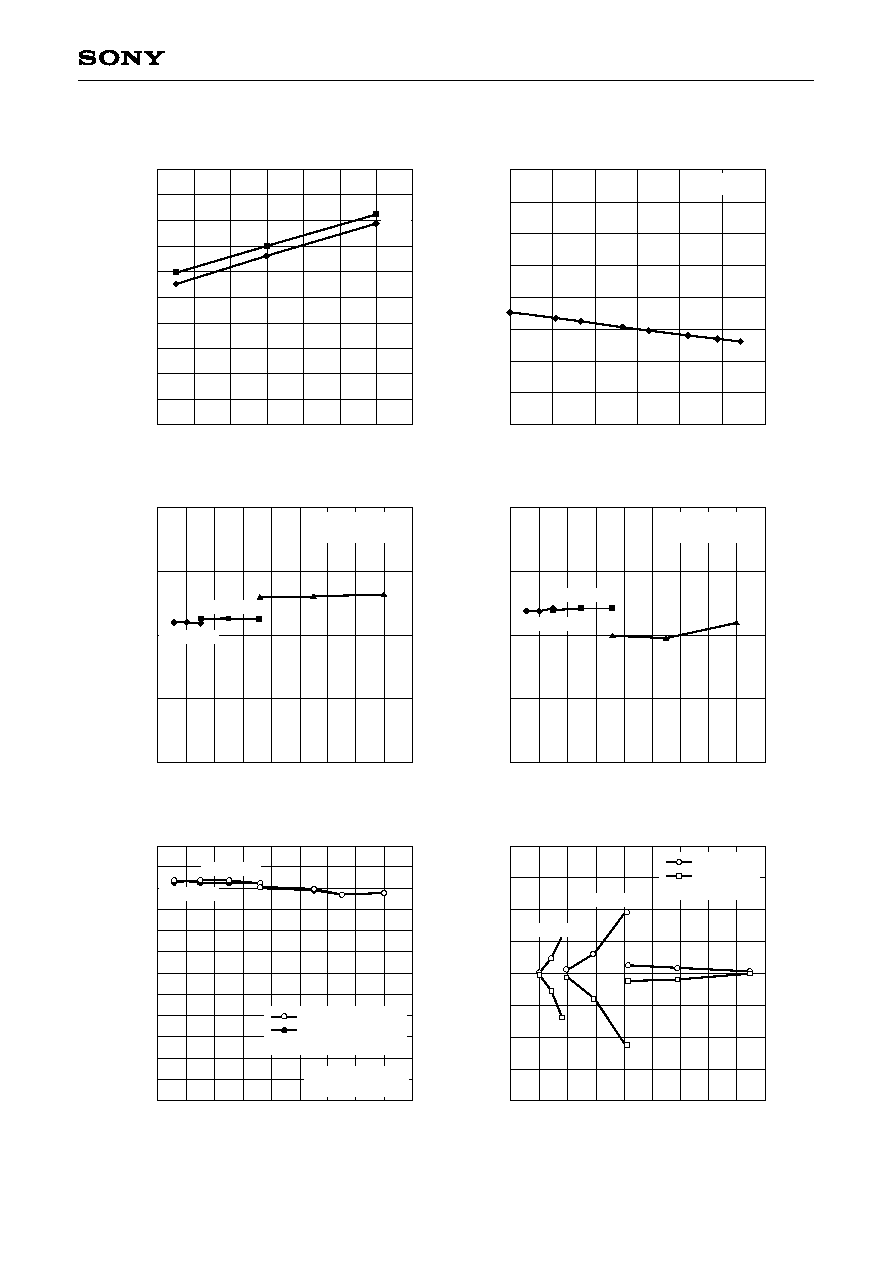
Example of Representative Characteristics
70
68
66
64
62
60
58
56
54
52
50
4.7
4.8
4.9
5.0
5.1
5.2
5.3
5.4
Vcc ≠ Supply voptage [V]
Icc
≠
Circuit current [mA]
Circuit current vs. Supply voltage
5.4
5.3
5.2
5.1
5.0
4.9
4.8
4.7
4.6
0
3
6
9
12
15
18
Output current [mA]
Output v
oltage [V]
Band SW output voltage vs. Output current
(BS1, BS2, BS3, BS4)
Vcc = 5V
40
30
20
10
0
0
100 200 300 400 500 600 700 800 900
Reception frequency [MHz]
CG
≠
Con
v
ersion gain [dB]
Conversion gain vs. Reception frequency
(Untuned input)
VHF (Low)
VHF (High)
UHF
f
IF
= 45MHz
High gain mode
20
15
10
5
0
0
100 200 300 400 500 600 700 800 900
Reception frequency [MHz]
NF
≠
Noise figure [dB]
Noise figure vs. Reception frequency
(Untuned input, in DSB)
VHF (Low)
VHF (High)
UHF
f
IF
= 45MHz
High gain mode
120
90
100
110
80
70
50
40
20
10
60
30
0
0
100 200 300 400 500 600 700 800 900
Reception frequency [MHz]
CM
≠
Cross modulation [dBµ]
Next adjacent cross modulation vs. Reception frequency
(Untuned input)
VHF (Low)
VHF (High)
UHF
f
IF
= 45MHz
High gain mode
400
200
300
100
0
≠100
≠300
≠200
≠400
0
100 200 300 400 500 600 700 800 900
Oscillation frequency [MHz]
+B dr
ift [kHz]
Oscillation frequency power supply fluctuation
(PLL off)
VHF (Low)
VHF (High)
UHF
f
UD
= f
D
+ 12MHz
f
UD
= f
D
≠ 12MHz
(100kHz, 30% AM)
Vcc + 5%
Vcc ≠ 5%
(Vcc = 5V)
VHF
UHF
≠ 20 ≠
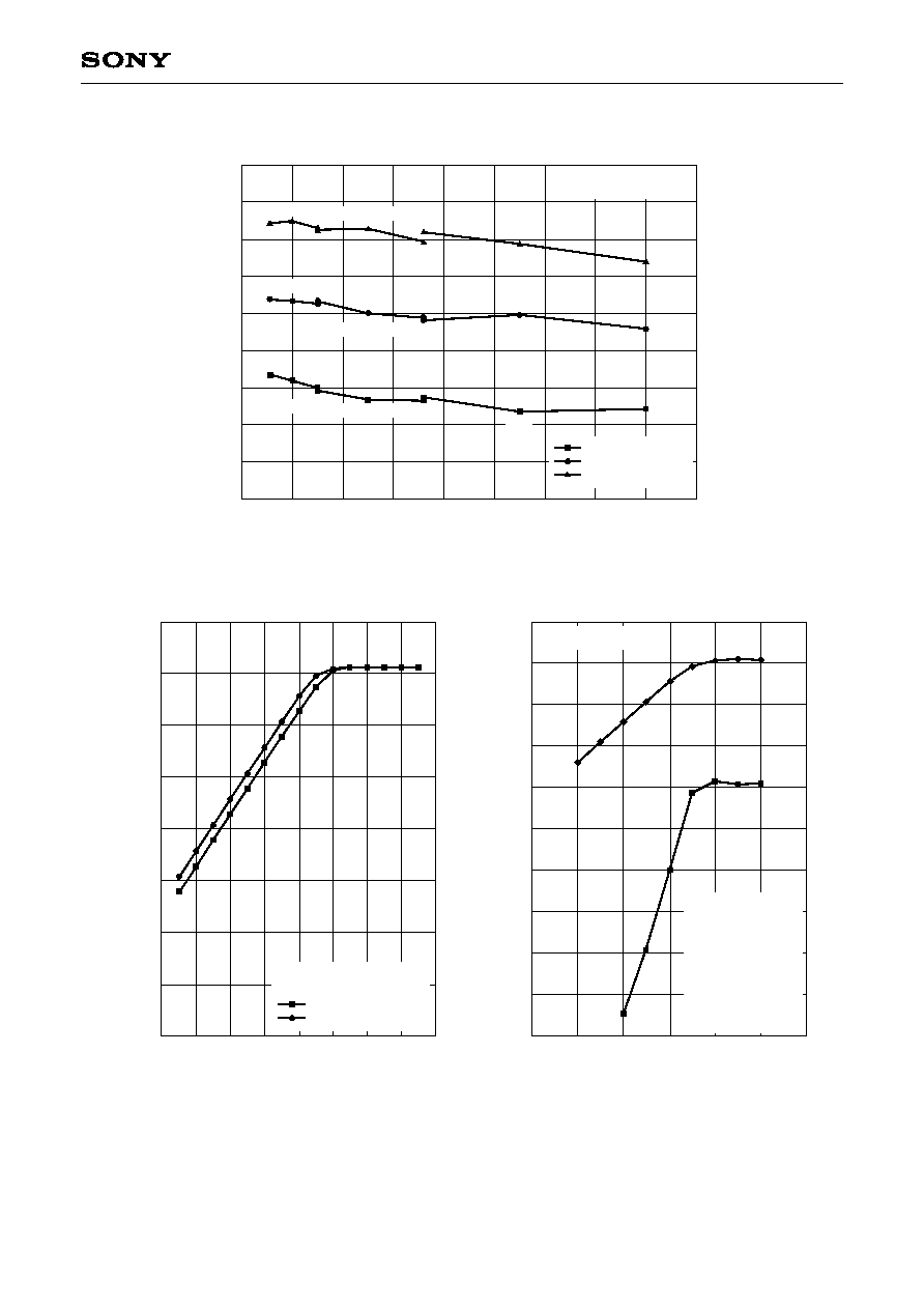
CXA3627N
1kHz offset
10kHz offset
100kHz offset
f
IF
= 45MHz
High gain mode
VHF (Low)
VHF (Low)
VHF (Low)
VHF (High)
VHF (High)
VHF (High)
UHF
UHF
UHF
130
120
110
100
90
80
70
60
50
40
0
100
200
300
400
500
Reception frequency [MHz]
C/N
≠
Oscillator phase noise [dBc/Hz]
Oscillator phase noise vs. Reception frequency (untuned input)
600
700
800
900
20
10
0
≠10
≠20
≠30
≠40
≠50
≠60
≠60
≠50
≠40
≠30
≠20
≠10
0
10
20
RF level [dBm]
IF output le
v
el [dBm]
I/O characteristics (untuned input)
f
RF
= 145MHz (VHF)
f
RF
= 495MHz (UHF)
f
RF
= 45MHz
High gain mode
20
f
IF
f
Beat
10
0
≠10
≠30
≠20
≠40
≠50
≠70
≠60
≠80
≠40
≠30
≠20
≠10
0
10
20
RF level (SG Setting level) [dBm]
IF output le
v
el [dBm]
PCS beat characteristics (untuned input)
f
Local
= 495MHz
f
P
= 449.25MHz
fc = 452.83MHz
(f
P
≠12dB)
fs = 453.75MHz
(f
P
≠1.7dB)
f
IF
= 45.75MHz
f
Beat
= f
IF
± 950kHz
High gain mode
≠ 21 ≠
CXA3627N
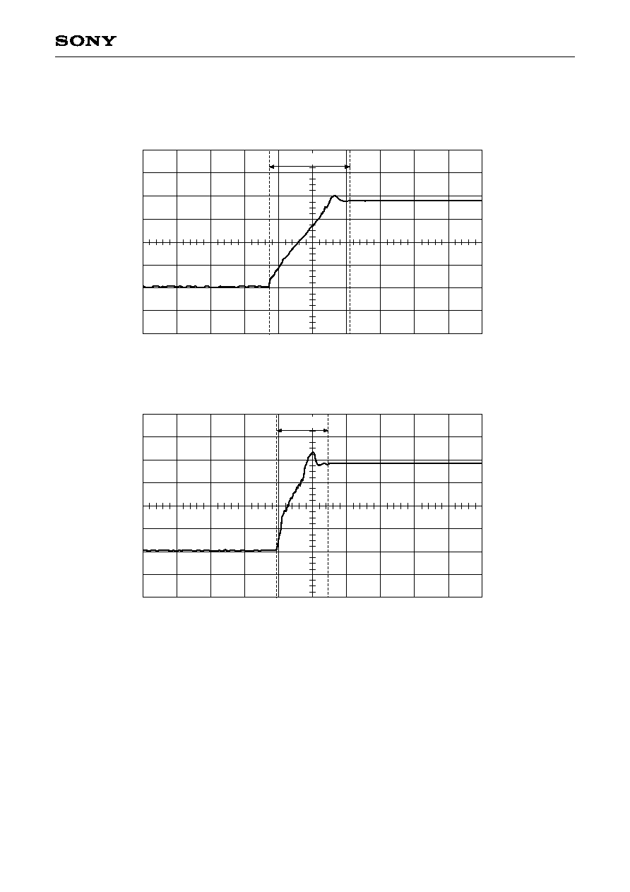
Tuning Response Time
≠75.0000ms
125.0000ms
25.0000ms
20.0ms/div
VHF (Low) 95MHz
VHF (High) 395MHz
5.0V/div
Offset 10.0V
T = 47.2ms
≠40.0000ms
60.0000ms
10.0000ms
10.0ms/div
5.0V/div
Offset 10.0V
T = 15.0ms
CP = 0
CP = 1
≠ 22 ≠
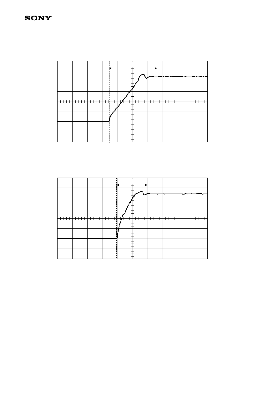
CXA3627N
≠70.0000ms
130.0000ms
30.0000ms
20.0ms/div
UHF 413MHz
UHF 847MHz
5.0V/div
Offset 10.0V
T = 63.6ms
≠40.0000ms
60.0000ms
10.0000ms
10.0ms/div
5.0V/div
Offset 10.0V
T = 20.2ms
CP = 0
CP = 1
≠ 23 ≠
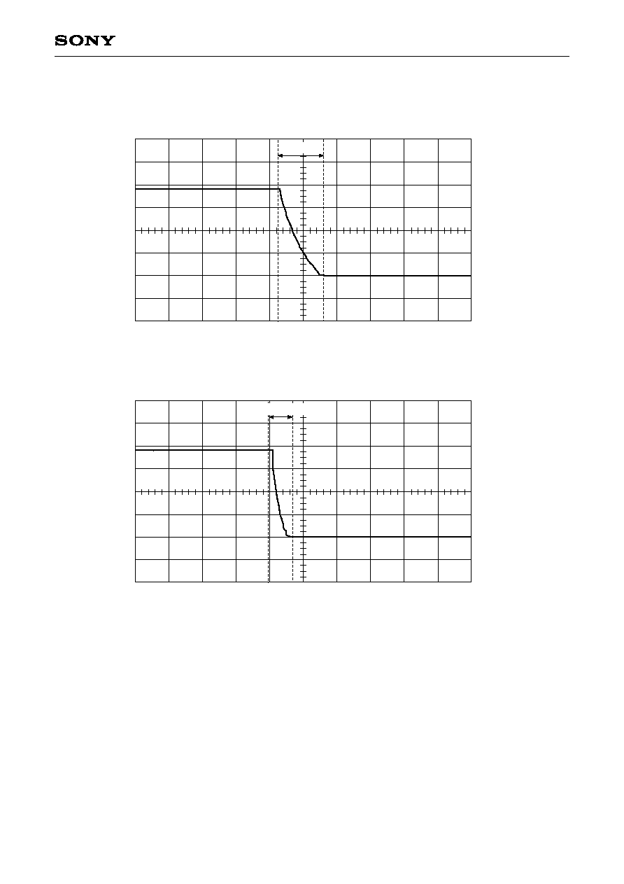
CXA3627N
≠110.0000ms
90.0000ms
≠10.0000ms
20.0ms/div
VHF (High) 395MHz
VHF (Low) 95MHz
5.0V/div
Offset 10.0V
T = 27.0ms
≠45.0000ms
55.0000ms
5.0000ms
10.0ms/div
5.0V/div
Offset 10.0V
T = 7.2ms
CP = 0
CP = 1
≠ 24 ≠
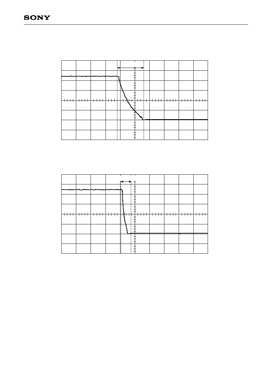
CXA3627N
≠110.0000ms
90.0000ms
≠10.0000ms
20.0ms/div
UHF 847MHz
UHF 413MHz
5.0V/div
Offset 10.0V
T = 35.6ms
≠90.0000ms
110.0000ms
10.0000ms
20.0ms/div
5.0V/div
Offset 10.0V
T = 14.4ms
CP = 0
CP = 1
≠ 25 ≠
CXA3627N
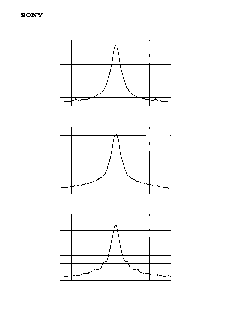
CENTER 45.00100MHz
RES BW 1.0kHz
VBW 10Hz
SPAN 50.00kHz
SWP 30.0s
REF = ≠10.0dBm
10dB/div
VHF (Low)
f
RF
= 55MHz
f
LO
= 100MHz
RF input level: ≠40dBm
CENTER 45.00350MHz
RES BW 1.0kHz
VBW 10Hz
SPAN 50.00kHz
SWP 30.0s
REF = ≠10.0dBm
10dB/div
VHF (High)
f
RF
= 350MHz
f
LO
= 395MHz
RF input level: ≠40dBm
CENTER 45.00188MHz
RES BW 1.0kHz
VBW 10Hz
SPAN 50.00kHz
SWP 30.0s
REF = ≠0.0dBm
10dB/div
UHF
f
RF
= 800MHz
f
LO
= 845MHz
RF input level: ≠40dBm
IF output spectrum

≠ 26 ≠
CXA3627N
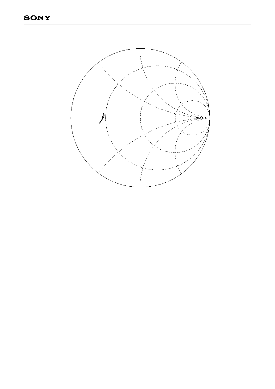
VHF Input Impedance
UHF Input Impedance
j50
0
50MHz
1000p
S11
350MHz
≠j50
≠j100
≠j25
j100
j25
11
12
50
j50
0
350MHz
1000p
S11
800MHz
≠j50
≠j100
≠j25
j100
j25
14
15
50
≠ 27 ≠
CXA3627N
IF Output Impedance
j50
0
45MHz
50
38MHz
≠j50
≠j100
≠j25
j100
j25
≠ 28 ≠
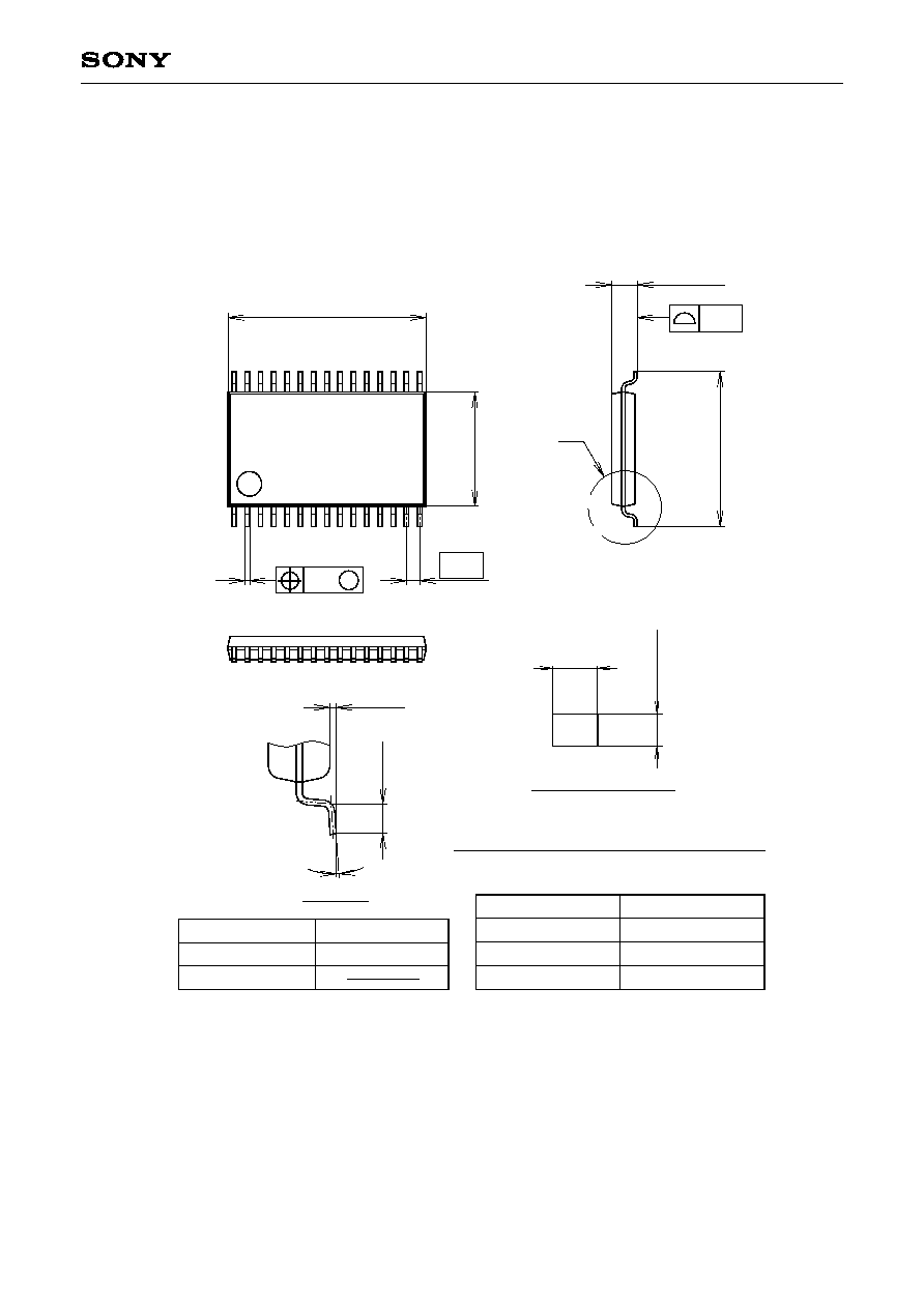
CXA3627N
SONY CODE
EIAJ CODE
JEDEC CODE
PACKAGE STRUCTURE
PACKAGE MATERIAL
LEAD TREATMENT
LEAD MATERIAL
PACKAGE MASS
EPOXY RESIN
30PIN SSOP (PLASTIC)
9.7 ± 0.1
5.6 ±
0.1
0.65
b
30
1
15
16
1.25
+ 0.2
≠ 0.1
7.6 ±
0.2
A
SSOP-30P-L01
P-SSOP30-5.6x9.7-0.65
0.1g
0.1 ± 0.1
0.5 ±
0.2
0∞ to 10∞
DETAIL A
0.10
0.13 M
NOTE: Dimension "
" does not include mold protrusion.
0.15 ≠ 0.01
DETAIL B : PALLADIUM
+ 0.03
b=0.22 ± 0.03
PALLADIUM PLATING
COPPER ALLOY
Sony Corporation
Package Outline Unit: mm