 | –≠–ª–µ–∫—Ç—Ä–æ–Ω–Ω—ã–π –∫–æ–º–ø–æ–Ω–µ–Ω—Ç: CXA7005R | –°–∫–∞—á–∞—Ç—å:  PDF PDF  ZIP ZIP |

≠ 1 ≠
E03426A35
Sony reserves the right to change products and specifications without prior notice. This information does not convey any license by
any implication or otherwise under any patents or other right. Application circuits shown, if any, are typical examples illustrating the
operation of the devices. Sony cannot assume responsibility for any problems arising out of the use of these circuits.
CXA7005R
48 pin LQFP (Plastic)
Description
The CXA7005R is a driver IC developed for use
with Sony polycrystalline silicon TFT LCD panels. It
supports 10-bit digital input, and the input data is
demultiplexed into 6 phases and output. The
CXA7005R can directly drive an LCD panel, and the
VCOM setting circuit and precharge pulse waveform
generator are also on-chip.
Features
∑ Supports 10-bit input
∑ Low output deviation
∑ Various adjustment functions using a 3-wire serial interface
∑ Supports signals up to XGA
∑ Supports dot and line inversion
∑ VCOM voltage generation circuit
∑ Precharge pulse waveform generation circuit
Applications
LCD projectors and other video equipment
Absolute Maximum Ratings (V
SS
= 0V)
∑ Supply voltage
V
CC
16
V
V
DD
5
V
∑ Operating temperature
Topr
≠20 to +70
∞C
∑ Storage temperature
Tstg
≠65 to +150
∞C
∑ Allowable power dissipation P
D
1200
mW
Recommended Operating Conditions
∑ Supply voltage
V
CC
15.0 to 15.5
V
V
DD
3.0 to 3.6
V
∑ Operating temperature
Topr
≠20 to +70
∞C
LCD Driver

≠ 2 ≠
CXA7005R
Block Diagram
DGND
D_IN0
D_IN1
D_IN2
D_IN3
D_IN6
D_IN7
D_IN8
D_IN9
DGND
D_IN5
D_IN4
CLK
FRP
PRG
DIRC
DGND
V
DD
AGND
AGND
AGND
STATUS
V
CC
FRINV
PV
CC
VCOM_OUT
SIG_OUT6
SIG_OUT5
SIG_OUT4
SIG_OUT3
SIG_OUT2
SIG_OUT1
SID_OUT
PV
CC
PGND
PGND
ADDR0
ADDR1
REF_IN
REF_OUT
AGND
AGND
V
CC
SENB
SCLK
SDAT
SIF
TG
SID
DC_GEN
D/A
D/A
D/A
D/A
D/A
D/A
Driver
REF
D/A
Driver
Driver
Driver
Driver
Driver
Digital
DGND
DGND
36
35
34
33
32
31
30
29
28
27
26
25
24
23
22
21
20
19
18
17
16
15
14
13
12
11
10
9
8
7
6
5
4
3
2
1
48
47
46
45
44
43
42
41
40
39
38
37

≠ 3 ≠
CXA7005R
Pin Description
Symbol
Equivalent circuit
Pin
No.
Description
I/O
Standard
voltage level
SENB
Enable input for 3-wire
serial interface.
Data is written only while
this pin is low.
I
High:
2.0V
Low:
0.8V
3
SCLK
Clock input for 3-wire
serial interface.
Supports a clock from
100kHz to 1MHz.
I
High:
2.0V
Low:
0.8V
4
SDAT
Data input for 3-wire
serial interface.
I
High:
2.0V
Low:
0.8V
5
ADDR0
ADDR1
IC address setting for
3-wire serial interface.
Addresses from 0h to 7h
can be set by changing
this setting.
I
High = V
DD
Low = GND
6
7
V
DD
1k
GND
3
V
DD
1k
GND
4
V
DD
1k
GND
5
V
DD
20k
GND
6
7
40k
40k
V
CC
GND
10
8k
8k
25µ
16k
16k
12.5µ
36k
145
2k
REF_IN
Reference voltage
(signal center) input.
When using multiple
CXA7005Rs, connect to
REF_OUT that differs
from the reference.
I
6.0V
10

≠ 4 ≠
CXA7005R
Symbol
Equivalent circuit
Pin
No.
Description
I/O
Standard
voltage level
REF_OUT
Signal center voltage
(inversion folded voltage)
output.
When using multiple
CXA7005Rs, connect to
REF_IN through a 1k
resistor.
O
6.0V
12
V
CC
GND
12
145
2k
2k
124k
VCOM_OUT
Common voltage output
of LCD panel.
Adjustment is possible
by the 3-wire serial
interface setting.
O
5.5 to 7.5V
Demultiplexed output of
AC inverse driven video
signals.
Can be directly
connected to the LCD
panel.
O
1.5 to 13.5V
SID_OUT
Precharge waveform
output.
Adjustment is possible
by the 3-wire serial
interface setting.
This pin cannot directly
drive the LCD panel, so
input to the LCD panel
through a buffer.
O
1.5 to 13.5V
FRINV
Input for switching the
output polarity to
inverted or non-inverted
relative to the LCD
panel AC drive inversion
timing (FRP) pulse.
I
High:
2.0V
Low:
0.8V
V
CC
1k
GND
13
1k
500
145
500
V
CC
PV
CC
GND
PGND
16
15
17
21
20
22
400
400
400
V
CC
PV
CC
GND
PGND
24
145
400
V
DD
20k
GND
29
13
15
16
17
20
21
22
24
29
SIG_OUT6
to
SIG_OUT1

≠ 5 ≠
CXA7005R
Symbol
Equivalent circuit
Pin
No.
Description
I/O
Standard
voltage level
STATUS
Master/slave setting
when using two
CXA7005Rs.
When set high, this chip
operates as the master
IC; when set low, this
chip operates as the
slave IC.
When using only one
CXA7005R, leave this
pin open.
I
High:
2.0V
Low:
0.8V
V
DD
20k
GND
30
30
DIRC
Scan direction setting.
The scan direction is set
in combination with the
3-wire serial interface
setting DIRCR.
I
High:
2.0V
Low:
0.8V
31
PRG
Timing pulse input for
switching the Pin 24
(SID_OUT) output level.
This pin is also used as
the circuit reset pulse.
I
High:
2.0V
Low:
0.8V
32
FRP
LCD panel AC drive
inversion timing input.
High: inverted
Low: non-inverted
I
High:
2.0V
Low:
0.8V
33
CLK
Dot clock input.
The polarity is
determined by the 3-wire
serial interface setting
CKPOL.
High: reverse polarity
Low: positive polarity
I
High:
2.0V
Low:
0.8V
34
V
DD
20k
GND
31
V
DD
1k
GND
32
V
DD
1k
GND
33
V
DD
1k
GND
34

≠ 6 ≠
CXA7005R
Symbol
Equivalent circuit
Pin
No.
Description
I/O
Standard
voltage level
D_IN9
to
D_IN0
Digital data input.
D_IN0: LSB
D_IN11: MSB
I
High:
2.0V
Low:
0.8V
37
to
46
V
DD
1k
GND
46
37 to
V
DD
V
CC
PV
CC
DGND
AGND
PGND
3.3V power supply.
15V power supply.
Power V
CC
.
GND.
GND.
Power GND.
3.3V
15.5V
15.5V
DGND
AGND
PGND
35
11, 25
14, 23
1, 2,
36,
47, 48
8, 9,
26, 27,
28
18, 19

≠ 7 ≠
CXA7005R
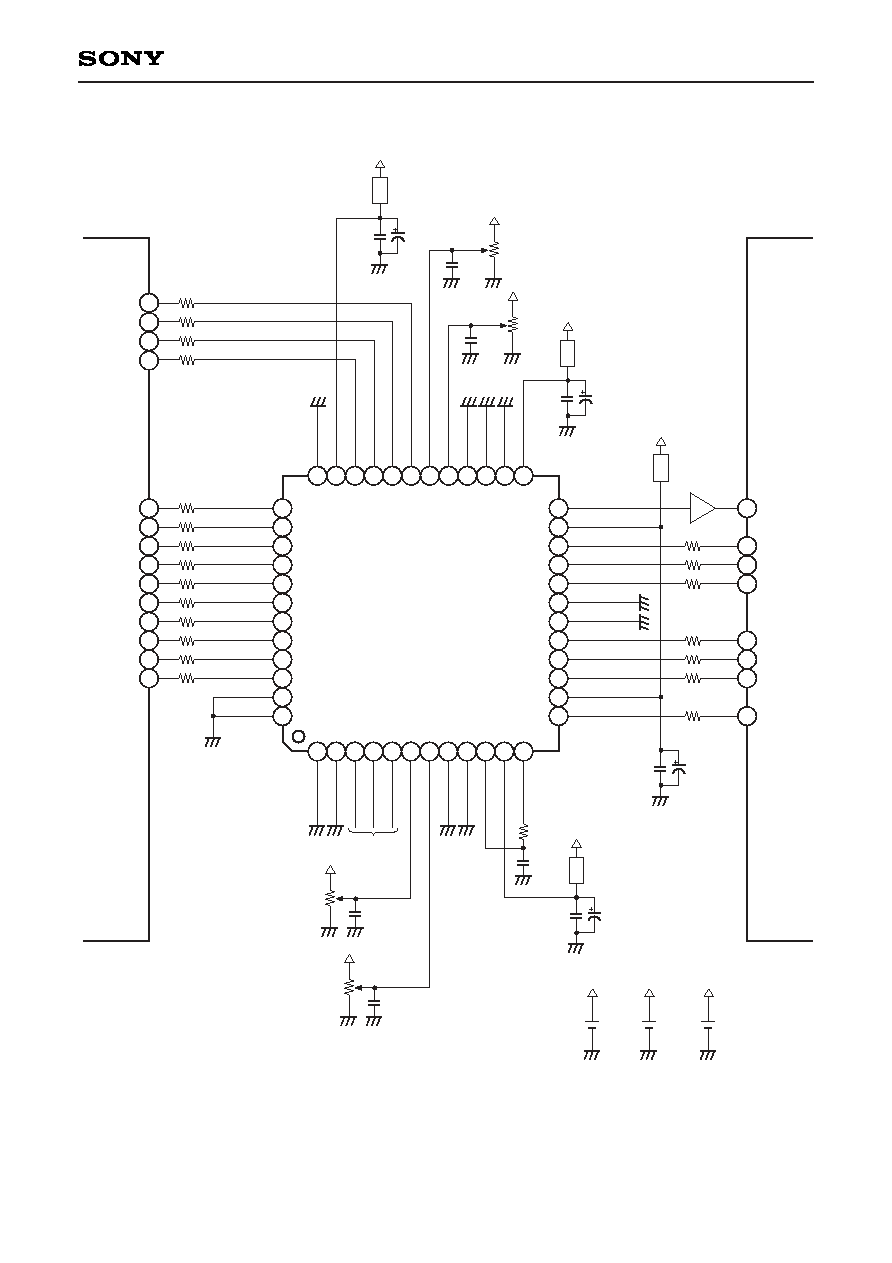
Electrical Characteristics Measurement Circuit
1
2
3
4
5
6
7
8
9
10
11
12
36
35
34
33
32
31
30
29
28
27
26
25
37
38
39
40
41
42
43
44
45
46
47
48
24
23
22
21
20
19
18
17
16
15
14
13
D_IN7
D_IN6
D_IN5
D_IN4
D_IN3
D_IN2
D_IN1
D_IN0
DGND
DGND
D_IN8
D_IN9
250pF
250pF
250pF
250pF
250pF
250pF
A
47pF
A
A
V
DD
V
DD
PV
CC
15.25V
V
CC
15.25V
V
DD
3.3V
CLK
FRP
PRG
DIRC
DGND
V
DD
AGND
AGND
AGND
STATUS
V
CC
FRINV
PV
CC
VCOM_OUT
SIG_OUT6
SIG_OUT5
SIG_OUT4
SIG_OUT3
SIG_OUT2
SIG_OUT1
SID_OUT
PV
CC
PGND
PGND
ADDR0
ADDR1
REF_IN
REF_OUT
AGND
AGND
V
CC
SENB
SCLK
SDAT
DGND
DGND

≠ 8 ≠
CXA7005R
Electrical Characteristics
(Ta = 25∞C)
Item
Symbol
Measurement description
Digital input
resolution
Digital input
setup time 1
Digital input
setup time 2
Digital input
hold time 1
Digital input
hold time 2
CLK input
frequency
range 1
CLK input
frequency
range 2
SIG_OUT output
voltage range
SIG_OUT output
amplitude
adjustable range
SIG_OUT
slew rate
SIG_OUT offset
adjustable range
Signal center
adjustable range
SID amplitude
adjustable range 1
SID amplitude
adjustable range 2
VCOM
adjustable range
V
DD
current
consumption
V
CC
current
consumption 2
n
Ts1
Ts2
Th1
Th2
f
CLK1
f
CLK2
V
SIGOUT
V
SIGOUTpp
SR
OUT
V
OFST
V
SIG
A
SID1
A
SID2
VCOM
I
DD
I
CC
CKPOL: 3.3V, PRG and D_IN[9:0] setup
time relative to CLK input.
CKPOL: 0V, PRG and D_IN[9:0] setup time
relative to CLK input.
CKPOL: 3.3V, PRG and D_IN[9:0] hold
time relative to CLK input.
CKPOL: 0V, PRG and D_IN[9:0] hold time
relative to CLK input.
SLDAT: 3.3V, maximum frequency at which
the internal timing generator and D/A
converter operate normally.
SLDAT: 0V, maximum frequency at which
the internal timing generator and D/A
converter operate normally.
Output voltage range of SIG_OUT1 to
SIG_OUT6.
Gain control: 00h, measure the SIG_OUT
voltage difference at D_IN[9:0] = 000h and
3FFh.
Load capacitance C = 270pF; measure the
slew rate at 10 to 90% of SIG_OUT1 to
SIG_OUT6 rise and fall when D_IN[9:0] is
varied from 000h to 3FFh or from 3FFh to
000h.
Offset adjustable range of SIG_OUT1 to
SIG_OUT6 by Bright control.
Signal center voltage adjustable range
when SIG center is varied.
SID_OUT amplitude adjustable range by
SID control A.
SID_OUT amplitude adjustable range by
SID control B.
VCOM_OUT adjustable range relative to
signal center voltage when VCOM control
is varied.
CLK = 80MHz, V
DD
current consumption.
CLK = 80MHz, inversion signal every
D_IN = 000h, FRP = 60CLK,
V
CC
+ PV
CC
current consumption when
SIG_OUT load capacitance = 250pF.
No.
1
2
3
4
5
6
7
8
9
10
11
12
13
14
15
16
17
Min.
Typ.
Max.
Unit
10
--
--
--
--
--
--
--
--
--
--
--
--
--
--
--
--
--
--
--
--
--
100
80
13.5
6
--
1.175
8.625
6
6
0
28
68
bit
ns
ns
ns
ns
MHz
MHz
V
V
V/µs
V
V
V
V
V
mA
mA
--
0
0.5
2.5
2
--
--
1.5
2
170
0
6.375
0
0
≠2
23
38

≠ 9 ≠
CXA7005R
Item
Symbol
Measurement description
Output deviation
between
SIG_OUT
channels 1
Output deviation
between
SIG_OUT
channels 2
Output deviation
between
SIG_OUT ICs 1
Output deviation
between
SIG_OUT ICs 2
MAINDAC
differential
linearity error
D
OUT1
D
OUT2
D
IC1
D
IC2
DLE
D_IN[9:0] = 1FFh, value obtained by
subtracting minimum value from maximum
value of SIG_OUT1 to SIG_OUT6 output
at Gain control = BFh.
D_IN[9:0] = 000h or 3FFh, value obtained
by subtracting minimum value from
maximum value of SIG_OUT1 to SIG_OUT6
at Gain control = BFh.
D_IN[9:0] = 1FFh, value obtained by
subtracting minimum value from maximum
value of SIG_OUT1 to SIG_OUT6 at
Gain control = BFh.
D_IN[9:0] = 000h or 3FFh, value obtained
by subtracting minimum value from
maximum value of SIG_OUT1 to SIG_OUT6
at Gain control = BFh.
MAINDAC differential linearity error
No.
18
19
20
21
22
Min.
Typ.
Max.
Unit
--
--
--
--
--
5
10
5
10
1
mV
mV
mV
mV
LSB
--
--
--
--
≠1

≠ 10 ≠
CXA7005R
3-wire Serial Interface
The CXA7005R makes the various register settings using a 3-wire serial interface.
Up to 8 IC addresses can be designated by the ADDR0 and ADDR1 (Pins 6 and 7) settings, and these
settings can be adjusted individually. The relationship between the IC address and ADDR0 and ADDR1 is
shown below. In addition, the adjustable settings include the mode settings, gain, offset, signal center voltage,
precharge, and common voltage (VCOM) settings. (See the Register Function Setting Table.)
AC Characteristics
(Topr = ≠20 to +75∞C, V
DD
= 3.3 ± 0.3V, V
SS
= 0V)
Timing Definition
Max.
--
--
--
--
Min.
100
100
100
100
Typ.
--
--
--
--
Symbol
tes
teh
tds
tdh
Item
SENB setup time relative to the rising edge of SCLK
SENB hold time relative to the rising edge of SCLK
SDAT setup time relative to the rising edge of SCLK
SDAT hold time relative to the rising edge of SCLK
Unit
ns
ns
ns
ns
V
DD
SENB
tes
teh
tdh
tds
SCLK
SDAT
V
SS
V
DD
V
SS
V
DD
V
SS
ENABLE high
400ns

≠ 11 ≠
CXA7005R
Input Format
Write Designation Byte
Write designation byte
Data
Dummy data
SENB
SCLK
SDAT
0
D2
D1
D0
0
REG
ADDR2
REG
ADDR1
REG
ADDR0
SENB
SCLK
SDAT
IC address
Register address
Input Format and Initialization
The 3-wire serial interface input format is shown below.
The minimum configuration is the 3 bytes of one write designation byte, one data byte, and one dummy data
byte. In addition, the register address is automatically incremented by the number of input data.
∑ Initialization
This IC must initialize the registers before setting the registers. Write "1" to register address (00h) RESET after
power is turned on. This setting initializes this IC.
After initialization, register setting is performed by returning RESET to "0". When initialization is not performed,
the setting value of a register may not be reflected correctly.
External pin
L
L
L
C
C
H
H
H
L
C
H
L
H
L
C
H
IC address
0
1
2
3
4
5
6
7
ADDR1
ADDR0
D2
L
L
L
L
H
H
H
H
D1
L
L
H
H
L
L
H
H
D0
L
H
L
H
L
H
L
H
IC address for serial interface
L: GND
C: 1/2V
DD
or OPEN
H: V
DD
IC Address Definition

≠ 12 ≠
CXA7005R
Register Function Setting Table
D2
SIDON
SIGC2
G2
B2
VC2
SIDA2
SIDB2
D1
PRPOL
SIGC1
G1
B1
VC1
SIDA1
SIDB1
D0
CKPOL
SIGC0
G0
B0
VC0
SIDA0
SIDB0
D5
SLINV
SIGC5
G5
B5
VC5
SIDA5
SIDB5
D4
FHCNT
SIGC4
G4
B4
VC4
SIDA4
SIDB5
D3
DIRCR
SIGC3
G3
B3
VC3
SIDA3
SIDB3
D7
RESET
G7
B7
D6
SIDAT
G6
B6
VC6
SIDA6
SIDB6
Function
Mode
SIG center
Gain control
Bright control
VCOM control
SID control A
SID control B
REG ADDR
00
01
02
03
04
05
06
Mode:
Various function settings
SIG center:
Signal center voltage setting
Gain control:
Voltage amplitude setting between SIG_OUT white and black levels
Bright control: Offset adjustment from SIG_OUT signal center voltage
VCOM control: VCOM voltage setting
SID control A: Precharge signal voltage setting A
SID control B: Precharge signal voltage setting B
≠ 13 ≠
CXA7005R
Description of Operation
The flow of internal operations is described below.
The digital signals input to D_IN0 to D_IN9 are internally demultiplexed into 6 phases, and then data processed
according to the various mode settings. After that, the signals are D/A converted into analog signals for each
channel, amplified at the rear end, and output.
The output level relative to the output level setting changes according to the following settings.
A: Register Gain control setting
B: Register Bright control setting
C: Signal center voltage
∑ Signal center voltage adjustment (C)
The signal center voltage is determined by the register setting SIG center.
The signal center voltage can be adjusted in 35mV/LSB steps from 00h: 6.5V to 3Fh: 8.5V.
∑ Offset adjustment relative to the signal center voltage (B)
The output voltage at digital input 3FFh is determined by the SIG_C voltage and the register setting Bright
control.
The offset relative to the signal center voltage can be adjusted in 4mV/LSB steps from 00h: SIG_C ± 0.2V to
FFh: SIG_C ± 1V.
∑ White-black amplitude gain adjustment (A)
The white-black voltage amplitude when the digital input is varied from 000h to 3FFh is determined by the
register setting Gain control in the condition with the white level fixed.
The gain relative to the signal center voltage can be adjusted in 16mV/LSB steps from 00h: SIG_C ± 2V to
FFh: SIG_C ± 5.5V.
1023
512
0
B
B
A
A
C
Digital IN
SIG_OUT
≠ 14 ≠
CXA7005R
Other settings are as follows.
Mode setting
The CXA7005R can be set to master/slave mode, single mode, and right/left inversion, etc. This makes it
possible to support various systems. (Various mode setting is designated with register and external pins.)
The various operating modes are described below.
∑ Operating mode setting <SLDAT>
The digital input of two ICs can be used together in master/slave mode by setting the Mode setting: SLDAT to
high level, or single mode can be set by setting SLDAT to low level. In master/slave mode, the 10-bit input is
shorted between the two ICs, and the ODD or EVEN data is selected by STATUS (Pin 30), DIRC (Pin 31) and the
Mode setting: DIRCR. Input a clock having the same period as the input data rate to CLK (Pin 34) in both modes.
SLDAT: L
SIG_OUT1: 1
SIG_OUT2: 2
SIG_OUT3: 3
SIG_OUT4: 4
SIG_OUT5: 5
SIG_OUT6: 6
SIG_OUT1: 6
SIG_OUT2: 5
SIG_OUT3: 4
SIG_OUT4: 3
SIG_OUT5: 2
SIG_OUT6: 1
SLDAT: H
SIG_OUT1: 2
SIG_OUT2: 4
SIG_OUT3: 6
SIG_OUT4: 8
SIG_OUT5: 10
SIG_OUT6: 12
SIG_OUT1: 11
SIG_OUT2: 9
SIG_OUT3: 7
SIG_OUT4: 5
SIG_OUT5: 3
SIG_OUT6: 1
SIG_OUT1: 1
SIG_OUT2: 3
SIG_OUT3: 5
SIG_OUT4: 7
SIG_OUT5: 9
SIG_OUT6: 11
SIG_OUT1: 12
SIG_OUT2: 10
SIG_OUT3: 8
SIG_OUT4: 6
SIG_OUT5: 4
SIG_OUT6: 2
DIRC ex-or DIRCR: H
DIRC ex-or DIRCR: L
STATUS: L
STATUS: H
∑ Clock polarity setting <CKPOL>
The polarity of the internal circuit operation clock (MCLK) is determined by the Mode setting: CKPOL.
The internal circuits operate at reverse polarity from CLK when CKPOL is high, and at the same polarity as CLK
when CKPOL is low.
1
2
3
4
5
6
7
8
9
10
11
12
13
14
15
Input data D_IN[9:0]

≠ 15 ≠
CXA7005R
∑ Horizontal sync timing <PRPOL>
The horizontal sync signal PRG is also used as the internal circuit reset function.
The Mode setting: PRPOL sets whether to apply the reset at the rising edge or the falling edge of PRG.
The reset is applied at the rising edge of the PRG pulse when PRPOL is high, and at the falling edge of the
PRG pulse when PRPOL is low.
∑ Output phase setting <FHCNT>
The SIG_OUT output timing phase can be set by the Mode setting: FHCNT.
When FHCNT is low, all SIG_OUT outputs are output at the same timing. When FHCNT is high, SIG_OUT1 to
SIG_OUT3 and SIG_OUT4 to SIG_OUT6 are output at phases offset by 1/2 clock period from each other.
∑ Polarity setting <FRINV>
Output polarity inversion/non-inversion relative to the signal center voltage is set by the FRP input and the
external pin FRINV (Pin 29). When set to the combinations shown in the table below, SIG_OUT is output non-
inverted (solid line) or inverted (dotted line) relative to FRP.
FRINV: H
Non-inverted
Inverted
FRP: H
FRP: L
FRINV: L
Inverted
Non-inverted
FRP
SIG_C
SIG_OUT
GND
Inverted
Non-inverted
PRG
MCLK
Reset pulse
PRPOL: H
PRPOL: L
SIG_OUT4 to 6
SIG_OUT1 to 3
GND
SIG_OUT4 to 6
SIG_OUT1 to 3
GND
FHCNT: L
FHCNT: H

≠ 16 ≠
CXA7005R
∑ Dot inversion and line inversion mode setting <SLINV>
When Mode setting: SLINV is set to low level, all SIG_OUT channels are output at the same polarity as shown
by the solid line in the figure below. When set to high level, the odd-numbered and even-numbered SIG_OUT
outputs are output at inverse polarities. At this time the odd-numbered outputs are inverted when the FRP
pulse is high, and non-inverted when the FRP pulse is low. Conversely, the even-numbered outputs are
inverted when the FRP pulse is low, and non-inverted when the FRP pulse is high.
FRP
SIG_C
SIG_OUT
GND
Inverted
Non-inverted
≠ 17 ≠
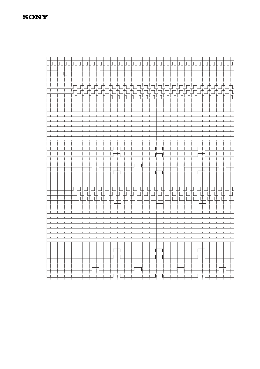
CXA7005R
Master/Slave mode
D_IN
CLK
PRG
PRG_X
ENB_F
ENB_F
CNT6
SOUT1
SOUT2
SOUT3
SOUT4
SOUT5
SOUT6
FHCNT: L
STB1_3
STB4_6
STB1_3
STB4_6
FHCNT: H
ENB
RCLK
CNT6
SOUT1
SOUT2
SOUT3
SOUT4
SOUT5
SOUT6
FHCNT: L
STB1_3
STB4_6
STB1_3
STB4_6
FHCNT: H
ENB
RCLK
0 1 2 3 4 5 6 7 8 9 10 11 12 13 14 15 16 17 18 19 20 21 22 23 24 25 26 27 28 29 30 31 32 33 34 35 36 37 38 39 40 41 42 43 44
1
13
3
15
5
17
7
19
9
21
11
23
45
2
14
4
16
6
18
8
20
10
22
12
24
STATUS: H
DIRC ex-or DIRCR: H
STATUS: L

≠ 18 ≠
CXA7005R
Master/Slave mode
D_IN
CLK
PRG
PRG_X
ENB_F
ENB_F
CNT6
SOUT1
SOUT2
SOUT3
SOUT4
SOUT5
SOUT6
FHCNT: L
STB1_3
STB4_6
STB1_3
STB4_6
FHCNT: H
ENB
RCLK
CNT6
SOUT1
SOUT2
SOUT3
SOUT4
SOUT5
SOUT6
FHCNT: L
STB1_3
STB4_6
STB1_3
STB4_6
FHCNT: H
ENB
RCLK
0 1 2 3 4 5 6 7 8 9 10 11 12 13 14 15 16 17 18 19 20 21 22 23 24 25 26 27 28 29 30 31 32 33 34 35 36 37 38 39 40 41 42 43 44
12
24
10
22
8
20
6
18
4
16
2
14
45
11
23
9
21
7
19
5
17
3
15
1
13
STATUS: H
DIRC ex-or DIRCR: L
STATUS: L

≠ 19 ≠
CXA7005R
Single mode
D_IN
CLK
PRG
PRG_X
CNT6
SOUT1
SOUT2
SOUT3
SOUT4
SOUT5
SOUT6
FHCNT: L
STB1_3
STB4_6
STB1_3
STB4_6
FHCNT: H
ENB, ENB_F
CNT6
SOUT1
SOUT2
SOUT3
SOUT4
SOUT5
SOUT6
FHCNT: L
STB1_3
STB4_6
STB1_3
STB4_6
FHCNT: H
ENB, ENB_F
0 1 2 3 4 5 6 7 8 9 10 11 12 13 14 15 16 17 18 19 20 21 22 23 24 25 26 27 28 29 30 31 32 33 34 35 36 37 38 39 40 41 42 43 44
6
7
8
9
10
11
12
13
14
15
16
17
18
19
20
21
22
23
24
25
26
27
28
29
0
6
12
18
24
0
1
7
13
19
25
1
2
8
14
20
26
2
3
9
15
21
27
3
4
10
16
22
28
4
5
11
17
23
29
5
45
DIR (DIRC ex-or DIRCR): H
DIR (DIRC ex-or DIRCR) : L

≠ 20 ≠
CXA7005R
SID Signal Generator Block
This circuit generates the precharge signal waveform used by the LCD panel.
The SID_OUT output level switching function is set on and off by the Mode setting (D2): SIDON.
When SIDON is low level, adjustment uses only the register setting: SID control A. When SIDON is high level,
adjustment is possible using both the register settings: SID control A and SID control B.
In addition, the SID_OUT output level relative to the signal center voltage can be set by the register settings:
SID control A and SID control B. Adjustment is possible in 50mV/LSB steps from 00h: SIG_C ± 5.5V to 7Fh:
SIG_C ± 0.1V for both settings.
SID_OUT cannot directly drive the precharge signal input of the LCD panel, so it should be connected through
a buffer having sufficient current supply capability.
VCOM Voltage Generator Block
This block sets the DC common potential for the LCD panel.
The SIG_OUT center potential set by the SIG_C voltage can be adjusted by the register setting VCOM control.
Adjustment is possible in 17.5mV/LSB steps from 00h: SIG_C ≠ 2V to 7Fh: SIG_C ≠ 0.1V.
SIDON: H
Adjusted by
SIDA6 to SIDA0
Adjusted by
SIDB6 to SIDB0
SIDON: L
Adjusted by only
SIDA6 to SIDA0
SID_OUT
SIG_C

≠ 21 ≠
CXA7005R
Example of Representative Characteristics (V
CC
= 15.25V, V
DD
= 3.3V, Ta = 25∞C)
0
6.0
6.5
7.0
7.5
8.0
8.5
9.0
60
50
40
30
20
10
1.0
1.5
2.5
2.0
3.0
3.5
4.0
4.5
5.0
5.5
6.0
250
200
150
100
50
0
50
100
150
200
250
0
6.0
6.5
7.0
7.5
8.0
8.5
9.0
0
5.0
5.5
6.0
6.5
7.0
7.5
8.0
120
100
80
60
40
20
20
40
60
80
100
120
0
0
1.0
0.5
2.0
1.5
2.5
3.5
3.0
4.5
4.0
6.0
5.5
5.0
7.0
6.5
7.5
8.0
400
200
600
800
1000
0
0
1
3
2
4
6
5
9
10
8
7
11
12
13
SIGC control characteristics
SIGC control code (DEC)
SIG_OUT [V]
Gain control characteristics
Gain control code (DEC)
SIG_OUT amplitude [V]
Bright control characteristics
Bright control code (DEC)
Inversion
SIG_OUT [V]
VCOM control characteristics
VCOM control code (DEC)
VCOM_OUT [V]
SID control characteristics
SID control code (DEC)
SID_OUT [V]
D_IN SIG_OUT characteristics
D_IN code (DEC)
Non-inverted SIG_OUT [V]
D_IN: 3FFh
SIGC: 00h to 3Fh
Bright: 00h
D_IN: 3FFh
SIGC: 20h
Bright: 00h to FFh
SIGC: 20h
SID A: 00h to 7Fh
SID B: 00h to 7Fh
D_IN: 000h to 3FFh
SIGC: 20h
GAIN: BFh
Bright: 00h
GAIN: 00h to FFh
VCOM: 00h to 7Fh
Inversion
Non-inversion
Non-inversion

≠ 22 ≠
CXA7005R
≠1.0
≠0.4
≠0.6
≠0.8
≠0.2
0
0.2
0.8
0.6
0.4
1.0
200
400
600
800
1000
MAINDAC DLE characteristics
D_IN code (DEC)
DLE
D_IN: 000h to 3FFh
≠ 23 ≠
CXA7005R
Application Circuit 1 -- Application Circuit to SVGA Panel
20k
0.1µF
1
2
3
4
5
6
7
8
9 10 11 12
36 35 34 33 32 31 30 29 28 27 26 25
37
38
39
40
41
42
43
44
45
46
47
48
24
23
22
21
20
19
18
17
16
15
14
13
D_IN7
D_IN6
D_IN5
D_IN4
D_IN3
D_IN2
D_IN1
D_IN0
DGND
DGND
D_IN8
D_IN9
V
CC
15.5V
PV
CC
15.5V
V
DD
3.3V
CLK
FRP
PRG
DIRC
DGND
V
DD
AGND
AGND
AGND
V
CC
FRINV
STATUS
PV
CC
VCOM_OUT
SIG_OUT6
SIG_OUT5
SIG_OUT4
SIG_OUT3
SIG_OUT2
SIG_OUT1
SID_OUT
PV
CC
PGND
PGND
ADDR0
ADDR1
REF_IN
REF_OUT
AGND
AGND
V
CC
SENB
SCLK
SDAT
DGND
DGND
Micro-
controller
FB
FB
47µF/35V
FB
LCD panel
(SVGA)
DSD
CXD3531R
FB
COM
Vsig6
Vsig5
Vsig4
Vsig3
Vsig2
Vsig1
Psig
D_IN7
D_IN6
D_IN5
D_IN4
D_IN3
D_IN2
D_IN1
D_IN0
D_IN8
D_IN9
CLK
FRP
PRG
RGT
10
10
10
10
10
10
10
10
10
10
10
10
10
10
10
10
10
10
10
10
10
Buffer
20k
0.1µF
20k
0.1µF
20k
0.1µF
CXA7005R
0.1µF
47µF/35V
0.1µF
47µF/35V
0.1µF
47µF/35V
1k
0.1µF
0.1µF
Application circuits shown are typical examples illustrating the operation of the devices. Sony cannot assume responsibility for
any problems arising out of the use of these circuits or for any infringement of third party patent and other right due to same.

≠ 24 ≠
CXA7005R
Application Circuit 2 -- Application Circuit to XGA Panel
20k
0.1µF
20k
0.1µF
20k
0.1µF
D_IN7
D_IN6
D_IN5
D_IN4
D_IN3
D_IN2
D_IN1
D_IN0
DGND
DGND
D_IN8
D_IN9
V
CC
15.5V
PV
CC
15.5V
V
DD
3.3V
CLK
FRP
PRG
DIRC
DGND
V
DD
AGND
AGND
AGND
V
CC
FRINV
STATUS
PV
CC
VCOM_OUT
SIG_OUT6
SIG_OUT5
SIG_OUT4
SIG_OUT3
SIG_OUT2
SIG_OUT1
SID_OUT
PV
CC
PGND
PGND
ADDR0
ADDR1
REF_IN
REF_OUT
AGND
AGND
V
CC
SENB
SCLK
SDAT
DGND
DGND
Micro-
controller
FB
FB
FB
LCD panel
(XGA)
DSD
CXD3531R
FB
COM
Vsig11
Vsig9
Vsig7
Vsig5
Vsig3
Vsig1
Psig
D_IN7
D_IN6
D_IN5
D_IN4
D_IN3
D_IN2
D_IN1
D_IN0
D_IN8
D_IN9
CLK
FRP
PRG
RGT
10
10
10
10
10
10
10
10
10
10
10
10
10
10
10
10
10
10
10
10
10
Buffer
20k
0.1µF
20k
0.1µF
20k
0.1µF
20k
0.1µF
20k
0.1µF
D_IN7
D_IN6
D_IN5
D_IN4
D_IN3
D_IN2
D_IN1
D_IN0
DGND
DGND
D_IN8
D_IN9
CLK
FRP
PRG
DIRC
DGND
V
DD
AGND
AGND
AGND
V
CC
FRINV
STATUS
PV
CC
VCOM_OUT
SIG_OUT6
SIG_OUT5
SIG_OUT4
SIG_OUT3
SIG_OUT2
SIG_OUT1
SID_OUT
PV
CC
PGND
PGND
ADDR0
ADDR1
REF_IN
REF_OUT
AGND
AGND
V
CC
SENB
SCLK
SDAT
DGND
DGND
Micro-
controller
FB
FB
Vsig12
Vsig10
Vsig8
Vsig6
Vsig4
Vsig2
10
10
10
10
10
10
CXA7005R
CXA7005R
47µF/35V
0.1µF
47µF/35V
0.1µF
47µF/35V
0.1µF
47µF/35V
0.1µF
47µF/35V
0.1µF
47µF/35V
0.1µF
1k
0.1µF
1
2
3
4
5
6
7
8
9 10 11 12
36 35 34 33 32 31 30 29 28 27 26 25
24
23
22
21
20
19
18
17
16
15
14
13
37
38
39
40
41
42
43
44
45
46
47
48
1
2
3
4
5
6
7
8
9 10 11 12
36 35 34 33 32 31 30 29 28 27 26 25
24
23
22
21
20
19
18
17
16
15
14
13
37
38
39
40
41
42
43
44
45
46
47
48
Application circuits shown are typical examples illustrating the operation of the devices. Sony cannot assume responsibility for
any problems arising out of the use of these circuits or for any infringement of third party patent and other right due to same.

≠ 25 ≠
CXA7005R
SONY CODE
EIAJ CODE
JEDEC CODE
PACKAGE MATERIAL
LEAD TREATMENT
LEAD MATERIAL
PACKAGE MASS
EPOXY RESIN
COPPER ALLOY
PACKAGE STRUCTURE
48PIN LQFP (PLASTIC)
9.0 ± 0.2
7.0 ± 0.1
1
12
13
24
25
36
37
48
(0.22)
0.18 ≠ 0.03
+ 0.08
0.2g
LQFP-48P-L01
P-LQFP48-7x7-0.5
(8.0)
0.5
±
0.2
0.127 ≠ 0.02
+ 0.05
A
1.5 ≠ 0.1
+ 0.2
0.1
PALLADIUM PLATING
NOTE: Dimension "
" does not include mold protrusion.
0.1 ± 0.1
0.5
±
0.2
0∞ to 10∞
DETAIL A
0.13 M
0.5
S
S
B
DETAIL B: PALLADIUM
0.127
±
0.04
0.18 ± 0.03
Sony Corporation
Package Outline Unit: mm