 | –≠–ª–µ–∫—Ç—Ä–æ–Ω–Ω—ã–π –∫–æ–º–ø–æ–Ω–µ–Ω—Ç: CXB1549 | –°–∫–∞—á–∞—Ç—å:  PDF PDF  ZIP ZIP |

CXB1549Q
Laser Diode Driver
Description
The CXB1549Q is a high-speed monolithic Laser
Diode Driver/Current Switch with ECL/PECL input
level. Open collector outputs are provided at the
output pins (Q, QBX) and have the capacity of driving
modulation current of 50mAp-p at a max. data rate of
1.25Gbps (Min.). Along with the modulation current
generator there is the laser diode bias generator
which has capacity of sourcing up to 60mA (Bias).
The laser diode current can be controlled by either a
voltage or current into the bias adjust pin (BiasAdj) and
the bias set pin (SBias), depending on how these
pins are configured. Control of the diode bias current
is achieved through the APC (Automatic Power
Control) circuitry. In order to avoid having a large
current go through the laser diode, this IC also
provides an Activity detector and Power on Reset
functions for Laser Safety. The Activity detector
circuit detects data edge transitions and if no data
transition occur after a certain time period, then both
the modulation and bias current are shutdown.
The Power on Reset circuit holds the modulation
and bias current off for a set period of time while the
system power is applied. Additionally, this IC has an
internal Duty Cycle correction circuit that can control
the falling edge of the input pulse up to a maximum
of 0.2ns (Min.).
Features
∑ Maximum data rate (NRZ): 1.25Gbps
∑ Power on Reset function
∑ Alarm and Shutdown function
∑ Signal Duty cycle correction
∑ Automatic Power Control (APC) for bias current
∑ Activity detector function for laser safety
∑ Power indicate function
∑ Differential PECL inputs or AC coupled inputs
Application
∑ Gbit-ethernet: 1.25Gb/s
∑ SONET/SDH: 622Mb/s
∑ Fibre channel: 532Mb/s, 1.062Gb/s
Absolute Maximum Ratings
∑ Supply voltage
Vcc ≠ V
EE
≠0.3 to +6.0
V
∑ Input voltage
V
IN
V
EE
to Vcc
V
∑ Differential input voltage
| V
D
≠ V
DB
|
0 to 2.5
V
∑ Bias output current
0 to 80
mA
∑ Modulation output current
0 to 70
mA
∑ SBias input/output current
0 to 5
mA
∑ Input bias control current
Iset (Ibiasadj)
0 to 5
mA
∑ Input bias control voltage
Vset (Vbiasadj)
0 to 3
V
∑ Storage temperature
Tstg
≠65 to +150
∞C
Recommended Operating Conditions
∑ DC power supply voltage
Vcc ≠ V
EE
3.14 to 3.46
V
∑ Operating ambient temperature
Ta
≠40 to +85
∞C
Structure
Bipolar silicon monolithic IC
≠ 1 ≠
E98313B92-PS
Sony reserves the right to change products and specifications without prior notice. This information does not convey any license by
any implication or otherwise under any patents or other right. Application circuits shown, if any, are typical examples illustrating the
operation of the devices. Sony cannot assume responsibility for any problems arising out of the use of these circuits.
40 pin QFP (Plastic)

≠ 2 ≠
CXB1549Q
Block Diagram and Pin Assignment
V
BB
Generator
V
REF
Power on
Reset
Reference
Generator
Bias
Circuit
DRV Cont
In_ALM
35
36
37
34
29
24
R
S
28
R
S
B
27
T
s
e
t
26
I
n
d
i
c
a
t
e
25
V
B
B
V
C
C
2
D
D
B
V
E
E
2
Q
V
E
E
5
B
i
a
s
S
B
i
a
s
V
C
C
4
23
22
21
20 ADCDis
16 CompB
15 CompA
19 TM
18 NC
17 Timer
14 DrvAdj
38
V
EE
3
CapZ
V
CC
3
V
REF
TEST_PIN
SDNB
SDN
LDAlm
39
APCOut
40
RsetPD
31
32
33
30
L
D
A
l
m
B
7
Q
B
X
8
V
E
E
1
9
V
E
E
1
10
DrvMon
11
V
EE
1
12
V
CC
1
13
6
5
4
1
V
E
E
4
2
B
i
a
s
A
d
j
3
Duty Cycle
Cont

≠ 3 ≠
CXB1549Q
Pin Description
Pad
No.
1
V
CC
4
3.3
Positive power supply
pin for APC circuit.
2
V
EE
4
0
Negative power supply
pin for APC circuit.
6
V
EE
5
0
Negative power supply
pin for Bias circuit.
7
Q
1.3 to 3.3
6mA to
30mA
1
6mA to
50mA
2
8
QBX
1.3 to 3.3
6mA to
30mA
1
6mA to
50mA
2
Laser modulation
current output pin.
Open collector output.
9, 10
V
EE
1
0
Negative power supply
pin for Driver circuit.
11
V
CC
1
3.3
Positive power supply
pin for Driver circuit.
12
V
EE
1
0
Negative power supply
pin for Driver circuit.
13
DrvMon
0µA
to
600µA
Sets Laser modulation
current (IQ) monitor pin.
IQ is monitored by
connecting a resistor
(Rmon) to this pin.
14
DrvAdj
0µA
to
600µA
Sets Laser modulation
current pin (IQ).
IQ is controlled by
connecting a resistor
(Rdrv) to this pin.
Refer to Fig.2.
3
BiasAdj
1.5 to 0
Sets Laser bias current
pin.
4
SBias
0mA
to
2.5mA
Sets Laser bias current
or monitor pin.
5
Bias
0mA
to
60mA
Laser bias current
output pin.
Open collector output.
Symbol
Typical voltage [V]
DC
AC
Equivalent circuit
Description
3
V
CC
V
EE
10pF
240
30
8
4
5
V
EE
7
8
Current
Source
V
CC
V
EE
1.3k
150 150
Rdrv
Rmon
13
14
1
Ta = ≠40 to 0∞C
2
Ta = 0 to +85∞C
Complementary current
output pin.
Q and QBX are
not symmetrical output.
Use Q output for Laser
modulation.

≠ 4 ≠
CXB1549Q
Pad
No.
15
CompA
Modulation current
driver compensation pin.
Normally, connects
180pF Capacitor across
CompA and CompB
pins.
16
CompB
Capacitor port pin for
activity detector
(IN_ALM) operation.
This pin set the period
of inactive time for
activity detector.
Inactive time is
controlled by connecting
a capacitor to this pin.
Refer to Fig.6.
17
Timer
No Connect pin.
18
NC
Chip temperature
monitor pin.
19
TM
1.5
This pin control the
activity detector Circuit.
High (connected to Vcc
or open): an activity
detector is disable.
Low (connected to V
EE
):
an activity detector is
enable.
20
ADCDis
V
EE
to
V
CC
(open)
Negative power supply
pin for Data input circuit.
21
V
EE
2
0
Symbol
Typical voltage [V]
DC
AC
Equivalent circuit
Description
V
CC
V
EE
30pF
180pF
10k
15
16
V
CC
2.1k
V
EE
17
10pF
200
µ
A
Ctimer
25
µ
A
2.4k
2.4k
V
EE
19
21
V
CC
V
EE
3.8k
3.8k
15
µ
A
35k
35k
35k
35k
20

≠ 5 ≠
CXB1549Q
Pad
No.
22
DB
1.6 to 2.4
23
D
1.6 to 2.4
24
V
CC
2
3.3
25
V
BB
2
26
Indicate
0.7 to 1.7
Differential PECL data
inputs pins.
These two inputs are
internally biased by
10k
to V
BB
.
Positive power supply
pin for Data input circuit.
Reference bias voltage.
(Option)
The analog voltage high
impedance output pin
which indicate of whether
the optical power of
Laser diode is operated
normal
or not. The power output
range has following
relationship.
High Light Indication;
Vo
1.7V
Nominal Operation;
Vo = 1.2V
Low Light Indication;
Vo
0.7V
Symbol
Typical voltage [V]
DC
AC
Equivalent circuit
Description
24
22
25
21
300
200
200
10k
10k
300
600
µ
A
23
600
µ
A
400
26
100k
V
CC
V
EE
14k
50
µ
A
35
µ
A
35
µ
A
27
Tset
Selector for output duty
cycle control pin.
This pin controls the
trailing edge of the input
high pulse. Variable
delay limit of that is from
0 to 0.2ns. Duty cycle is
controlled by connected
a resistor value between
Vcc and this pin.
Refer to Fig.1.
V
CC
V
EE
Rset
27
2.4k
2.4k
20pF
70
µ
A
140
220
28
RSB
0.5
29
RS
2.5
Window comparator
top/bottom threshold
voltage pin for
LD_ALARM.
The alarm (fail)
threshold assert voltage
can be set by the
external resistor.
Default voltages are
RS equal to 2.5V and
RSB equal to 0.5V.
29
28
V
CC
V
EE
100
µ
A
2.5k
20k
5k

≠ 6 ≠
CXB1549Q
Pad
No.
30
LDAlmB
0.2 to 3
31
LDAlm
0.2 to 3
32
SDN
0 to 3.3
33
SDNB
0 to 3.3
34
V
REF
1.7
Complementary open
collector TTL outputs.
Asserted when the fault
is detected in the Laser
monitor diode circuit.
Complementary TTL
inputs pin to disable
output current.
(shutdown input)
When left open = "High"
Temperature
compensated reference
voltage pin for APC.
1.7V (Constant for V
EE
reference)
Symbol
Typical voltage [V]
DC
AC
Equivalent circuit
Description
V
CC
V
EE
4.7k
4.7k
31
30
V
CC
V
EE
5k
5k
5k
5k
300
300
60
µ
A
60
µ
A
32
33
300
300
1.9mA
V
CC
V
EE
200
34
2.4k
9.1k
35
TEST_
PIN
OPEN
Do not connect.
36
V
CC
3
3.3
Positive power supply
pin for Signal Detect
circuit.

≠ 7 ≠
CXB1549Q
Pad
No.
37
CapZ
Capacitor and resistor
port pins for slow start
up. This pin controls the
initial turn-on time of
this IC (release time of
bias and modulation
current).
The time for this function
is set by an external RC
network.
Refer to Fig.7.
38
V
EE
3
0
Negative power supply
pin for Signal Detect
circuit.
39
APCOut
Output pin of APC OP-
Amp.
This signal control to
bias adjust pins.
(BiasAdj and SBias)
40
RsetPD
Monitor PD connect pin.
Symbol
Typical voltage [V]
DC
AC
Equivalent circuit
Description
3k
145
µ
A
V
CC
V
EE
200
Rseries
Cap_Z
37
145
µ
A
V
CC
V
EE
500
39
300
300
V
CC
V
EE
200
1.8mA
40
≠ 8 ≠
CXB1549Q
Electrical Characteristics
DC Electrical Characteristics
(V
CC
= 3.14 to 3.46V, V
EE
= 0V, Ta = ≠40 to +85∞C)
Item
DC Power supply voltage
Power supply current
Modulation output current range
Modulation output voltage range
Bias output current range
Bias output voltage range
Ratio of IB vs. Iset
ECL input High voltage
ECL input Low voltage
SDN, SDNB, Reset input High voltage
SDN,SDNB, Reset input Low voltage
LDA, LDAB output High voltage
LDA, LDAB output Low voltage
Reference bias voltage for OP Amp
Operating current range of V
REF
Vdc
I
EE
I
Q
1
I
Q
2
V
Q
I
B
V
B
IBvslset
V
EIH
V
EIL
V
TIH
V
TIL
V
TOH
V
TOL
V
REF
V
REF
drv
V
CC
≠ V
EE
I
Q
= 0mA, I
BIAS
= 0mA
Ta = ≠40 to 0∞C
Ta = 0 to +85∞C
I
OH
= ≠10µA, R
L
= 4.7k
I
OL
= 1mA, R
L
= 4.7k
3.14
≠76
6
6
V
CC
≠ 2
0
V
CC
≠ 2
14
V
CC
≠ 1.17
V
CC
≠ 1.84
2
0
V
CC
≠ 0.1
0
1.5
≠500
3.3
≠59
--
--
--
--
--
22
--
--
--
--
--
--
1.7
--
3.46
--
30
50
V
CC
60
V
CC
27
V
CC
≠ 0.81
V
CC
≠ 1.48
V
CC
0.8
V
CC
+ 0.2
0.4
1.9
+500
V
V
mA
V
--
µA
Symbol
Condition
Min.
Typ.
Max.
Unit
V
mA
Item
Maximum Data Rate
Rise time (20 to 80%)
Fall time (20 to 80%)
Max. variable High pulse width by
duty cycle control
Max. setting time range of IN_Alarm
Max. setting time range of POR
Shut down time
Shut down recovery time
fdmax
tr
tf
tdelay
ts_alm
ts_por
tsut_off
tsut_on
I
Q
= 20mA, R
L
= 25
I
Q
= 20mA, R
L
= 25
Data rate = 1.25Gbps
1.25
--
--
0.2
20
150
--
--
--
100
200
--
--
--
--
--
--
--
--
--
--
--
10
100
Gbps
ps
ns
µs
Symbol
Condition
Min.
Typ.
Max.
Unit
AC Electrical Characteristics
(V
CC
= 3.14 to 3.46V, V
EE
= 0V, Ta = ≠40 to +85∞C)

≠ 9 ≠
CXB1549Q
Item
Input voltage range
Output voltage range
Input bias current
Input offset voltage
Input offset Input current
Input impedance
Output drive current
Through rate
Open loop gain
Unity gain band-width
V
IN
V
O
I
B
V
OFF
I
OFF
Z
IN
I
O
SR
Av
funit
1.2
0.6
--
--
--
--
≠5.0
--
--
--
--
--
7
2.5
0.7
12
--
1.9
55
20
2.8
2
--
--
--
--
1.0
--
--
--
V
V
µA
mV
µA
k
mA
V/µs
dB
MHz
Symbol
Condition
Min.
Typ.
Max.
Unit
DC and AC Electrical Characteristics for OpAmp of APC Circuitry
(V
CC
= 3.14 to 3.46V, V
EE
= 0V, Ta = ≠40 to +85∞C)

≠ 10 ≠
CXB1549Q
Description of each function block
1. Data Buffer
Data Buffer is comprised of the data buffer and delay generator. ECL/PECL data is input to the data buffer at a
maximum data rate of 1.25Gbps. This data is buffered and input to the delay circuitry. The delay circuitry adds
a delay to the falling edge of the pulse up to a maximum of 0.2ns (Min.). The delay is set by a single external
resistor between the delay set pin (Tset-Pin 27) and Vcc. A plot of the high pulse width vs. set resistance
(Rset) is shown in Fig. 1.
2. V
BB
Generator
This circuit provides a reference bias voltage to the data buffer for AC coupling inputs.
3. Modulation Current Generator
This circuit can sink up to 50mA of current to modulate the laser diode. The modulation current is set by an
external resistor to Vcc at modulation current set pin (DrvAdj-Pin 14). There is also a modulation current
monitor pin (DrvMon-Pin 13) that allows the IC user to monitor the modulation current. By putting an external
fixed resistor between Vcc and DrvMon pin, you can monitor the modulation current by measuring the voltage
of DrvMon pin. The modulation current and monitor current are in the rate of approximately 50:1 (Refer to Figs.
8 and 9). A plot of the modulation current vs. setting resistance (Rdrv) is shown in Fig. 2.
4. Laser Diode Bias Current Generator
This circuit is a very large current source capable of sourcing up to 60mA of current to bias the laser diode on.
The circuit is a 22 to 1 (for current ≠ current setting) current mirror that can be controlled externally two ways.
The first of these is to tie the BiasAdj (Pin 3) and SBias (Pin 4) terminals together and inject a current into the
two terminals. The Bias (Pin 5) terminal is connected to the laser diode. Laser diode bias current vs. control
current (Iset) characteristics is shown in Fig. 3.
The second method of controlling the laser diode current is to ties the SBias (Pin 4) terminal to Vcc and tune
the BiasAdj (Pin 3) terminal with a voltage source. Varying the voltage at the BiasAdj terminal will vary the
current through the laser diode. Laser diode bias current vs. control voltage characteristics is shown in Fig. 4.
5. APC (Automatic Power Control) Circuitry
The APC Circuitry is comprised of the window comparator, APC OpAmp, laser diode alarm circuit and the
diode power indicator.
The APC OpAmp is normally configured as an inverting integrator. The inverting input is connected to the
photo diode that monitors the light intensity from the laser diode. The photo diode converts the received light
from the laser diode to a current. The output of the OpAmp then drives the laser diode current bias adjust pin,
and the laser diode bias set pin is held at Vcc via a resistor. With the OpAmp configured as an inverting
integrator, the OpAmp can tune the diode current inversely to the current in the photo diode. That is to say that
if a low current is detected by the photo diode the integrator output goes up causing more bias current to go
through the diode. If the photo diode current is high, then the output of the OpAmp will go low causing less bias
current to flow through the laser diode.
The output of the APC OpAmp drives a window comparator. The function of the window comparator is to
detect when the output of the APC OpAmp goes above or below a preset reference voltage for each
comparator (RS, RSB). When this happens the comparators outputs cause the laser diode alarm circuit
(LDAlm) to go high alerting the system that the laser diode current is either to high or to low.
The window comparator also drives the laser diode power indicator circuit (Indicate). This circuit is comprised
of two switches and one fixed current sources. When the APC OpAmp output is such that the laser diode bias
current is at its nominal set point, the output of the power indicator is at approximately 1.2Vdc. If the APC
OpAmp output goes low, the output of the power indicator increases to approximately 1.7Vdc, indicating a high
laser diode power condition. If the output of the APC OpAmp goes high, the output of the power indicator drops
to approximately 0.7Vdc.
Also connected to the output of the window comparator is laser alarm circuitry. This circuit alerts the user of
the device when the laser diode power level has risen either twice the normal set power or half the normal set
power. A high voltage at the laser diode alarm output indicates an alarm event. The laser diode alarm output is
disabled whenever a shutdown event is encountered.

≠ 11 ≠
CXB1549Q
6. Shutdown and Input Alarm Circuitry
This portion of the circuit disables both the modulation current driver and the laser diode bias generator under
various conditions. The function block diagram for all of the shutdown mechanisms for the circuit is shown in
Fig. 5. Shown below is the signal priority primarily for the reset function.
1) Power on Reset
2) Shutdown, Input Alarm
The Shutdown circuit has complementary TTL input to disable output current. Shown below is the desired truth
table for the shutdown function.
SDN
Low
Low
High
High
Low
High
Low
High
Off
On
Off
Off
SDNB
output current
The Activity detector (In_ALM) circuit is designed to detect an input pulse transition. If there is no input pulse
transition over a period time determined by the user, then the shutdown circuit is enabled causing the
modulation current and laser bias current to be shutdown. Inactive time is set by external capacitor value
between Timer pin (Pin 17) and V
CC
. Inactive time vs. Ctimer is shown in Fig.6.
The Power on reset circuit is an inverting comparator that has an external RC network with CapZ pin (Pin 37)
that is connected between Vcc and V
EE
. At power up, the RC begins to charge up towards the reference
voltage of the comparator. Since this is an inverting comparator the output will stay high until the capacitor
charges above the reference. As long as the comparator output is high, the laser diode is disabled. As soon as
the capacitor charges up beyond the reference, the output of the circuit goes low and the laser diode is
enabled and ready for normal operation. A plot of the power on reset time vs. capacitance for a 10k
resistor
(Rseries) is shown in Fig. 7.
In_ALM
Shutdown
SDN
Power on
Reset
SDNB
Power on
Reset
(CapZ)
D
DB
Timer ADCDis
Switch
To Modulation and
Bias Current
shutdown circuits
Fig.5. Shutdown and In_ALM Functional Block Diagram
7. Others
Pay attention to handling this IC because its electrostatic discharge strength is weak.
The Tset terminal (27pin) has to be connected through a resistor to Vcc.
Do not leave this pin open or connect to Vcc directly.

≠ 12 ≠
CXB1549Q
DC Electrical Characteristics Measurement Circuit
V
BB
Generator
V
REF
Power on
Reset
Reference
Generator
Bias
Circuit
DRV Cont
≠500 to
500
µ
A
180pF
0.1
µ
F
3.14 to
3.46V
In_ALM
35
36
37
34
29
24
28
27
26
25
23
22
21
20
16
15
19
18
17
14
38
39
40
31
32
33
30
7
8
9
10
11
12
13
6
5
4
1
2
3
Duty Cycle
Cont
4.7k
4.7k
1k
10k
1000pF
25
0 to 2V
≠10
µ
or 1mA
V
V
V
V
V
V
V
V
A
A
A
V
1k
V
2k
A
V
A

≠ 13 ≠
CXB1549Q
AC Electrical Characteristics Measurement Circuit
V
BB
Generator
V
REF
Power on
Reset
Reference
Generator
Bias
Circuit
DRV Cont
180pF
0.1
µ
F
1k
3.14 to
3.46V
In_ALM
35
36
37
34
29
24
28
27
26
25
23
22
21
20
16
15
19
18
17
14
38
39
40
31
32
33
30
7
8
9
10
11
12
13
6
5
4
1
2
3
Duty Cycle
Cont
4.7k
4.7k
10k
1000pF
1
µ
F
1
µ
F
25
100k
0.1
µ
F
0.1
µ
F
51
51
Spectrum
analizer
Oscilloscope
50
input
Z
0
=
5
0

≠ 14 ≠
CXB1549Q
Application Circuit (at V
CC
= 3.3V, V
EE
= 0V)
V
BB
Generator
V
REF
Power on
Reset
Reference
Generator
Bias
Circuit
DRV Cont
100pF
100pF
Ctimer
10k
V
CC
CapZ
Cpd
Rf
180pF
Rdry
Rset
0.1
µ
F
PECL input
V
CC
Indicate
510
3.3V
In_ALM
35
36
37
34
29
24
28
27
26
25
23
22
21
20
16
15
19
18
17
14
38
39
40
31
32
33
30
7
8
9
10
11
12
13
6
5
4
1
2
3
Duty Cycle
Cont
4.7k
LDAlm
V
C
C
4.7k
lset
Rs
15
5.1
R
I
Rpd
100pF
0.1
µ
F
20
LDAlmB
SDN
SDNB
Application circuits shown are typical examples illustrating the operation of the devices. Sony cannot assume responsibility for
any problems arising out of the use of these circuits or for any infringement of third party patent and other right due to same.
≠ 15 ≠
CXB1549Q
Example of Representative Characteristics
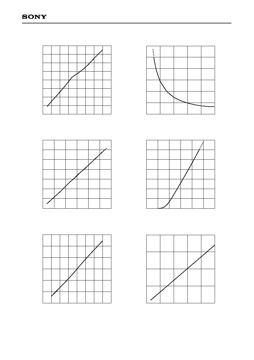
Fig. 1. Delay vs. Rset Characteristic
at 1ns input data pulse apply
0
≠0.4
≠0.3
≠0.2
≠0.1
0
0.4
0.3
0.2
0.1
1
2
3
4
Rset [k
]
F
a
l
l
i
n
g
e
d
g
e
d
e
l
a
y
[
n
s
]
5
6
7
8
Fig. 3. Bias Current (I
BIAS
) vs.
Bias adjust current (Iset) Characteristics
Fig. 2. Modulation Current (I
Q
) vs.
Rdrv Characteristics
I
Q
[
m
A
]
0
0
20
10
30
40
50
60
2
4
Rdrv [k
]
6
8
10
0
0
20
10
30
40
50
60
70
0.5
1
Iset [mA]
I
B
I
A
S
[
m
A
]
1.5
2
2.5
3
Fig. 6. Shutdown Time vs. Ctimer Characteristics
Fig. 4. Bias Current (I
BIAS
) vs.
Bias adjust voltage (Vset) Characteristics
Fig. 7. Power on Reset Time vs.
Cap_Z Characteristics (Rseries = 10k
)
0
0.0
0.5
1.0
1.5
2.0
2
4
Cap_Z [nF]
P
o
w
e
r
o
n
t
i
m
e
[
1
0
0
µ
s
]
6
8
10
0.4
0
20
10
30
40
50
60
70
0.6
0.8
Vset [V]
I
B
I
A
S
[
m
A
]
1
1.2
1.4
1.6
0.5
10
30
20
40
50
60
70
1
2
Ctimer [nF]
S
h
u
t
d
o
w
n
t
i
m
e
[
µ
s
]
3
4
1.5
2.5
3.5
4.5

≠ 16 ≠
CXB1549Q
I
Q
/I
DRVMON
(A) 3.14V
I
Q
/I
DRVMON
(A) 3.3V
I
Q
/I
DRVMON
(A) 3.46V
I
Q
/
I
D
R
V
M
O
N
R
ADJ
[k
]
0
0
20
40
60
80
100
5
10
15
20
25
I
Q
/Imon ≠40
∞
C 3.3V
I
Q
/Imon
0
∞
C 3.3V
I
Q
/Imon
27
∞
C 3.3V
I
Q
/Imon
85
∞
C 3.3V
I
Q
/
I
m
o
n
R
ADJ
[k
]
40
45
50
55
60
0
1
2
3
4
5
6
7
8
Fig. 8. Ratio of Modulation Current (I
Q
)/Modulation Monitor Current (I
DRVMON
) vs.
Rdrv Characteristics (Electrical)
Fig. 9. Ratio of Modulation Current (I
Q
)/Modulation Monitor Current (I
DRVMON
) vs.
Rdrv Characteristics (Temperature)

≠ 17 ≠
CXB1549Q
V
CC
= 0V
V
EE
= ≠3.3V
RL = 25
Ta = 27
∞
C
IQ = 30mA
Single input
Pattern = PRBS2
23
≠ 1
Data Rate 1.25Gbps
V
CC
= 0V
V
EE
= ≠3.3V
FP ≠ LD (
= 1330nm)
Ta = 27
∞
C
Single Input
Pattern = PRBS2
23
≠ 1
Data Rate 1.06Gbps
Filter (Cut Off 700Mbps)
Mask: FC1063
Ch.2 :5.0mV/div, Offset: 12.8mV
Bandwidth: 12.4GHz
Time Base:200ps/div
2
3
1
Ch.1 :150mV/div, Offset: ≠300mV
Bandwidth: 20.0GHz
Time Base : 200ps/div
Fig. 10. Electrical Output Waveform
Fig. 11. Optical Output Waveform

≠ 18 ≠
CXB1549Q
CXB1549Q
PIN#
1
2
3
4
5
6
7
8
9
10
11
12
13
14
15
16
17
18
19
20
V
CC
4
V
EE
4
BiasAdj
SBias
Bias
V
EE
5
Q
QBX
V
EE
1
V
EE
1
V
CC
1
V
EE
1
DrvMon
DrvAdj
CompA
CompB
Timer
NC
TM
ADCDis
21
22
23
24
25
26
27
28
29
30
31
32
33
34
35
36
37
38
39
40
V
EE
2
DB
D
V
CC
2
V
BB
Indicate
Tset
RSB
RS
LDAlmB
LDAlm
SDN
SDNB
V
REF
TEST_PIN
V
CC
3
CapZ
V
EE
3
APCOut
RsetPD
PIN NAME
PIN#
PIN NAME

≠ 19 ≠
CXB1549Q
Package Outline
Unit: mm
SONY CODE
EIAJ CODE
JEDEC CODE
PACKAGE MATERIAL
LEAD TREATMENT
LEAD MATERIAL
PACKAGE MASS
EPOXY RESIN
SOLDER / PALLADIUM
42/COPPER ALLOY
PACKAGE STRUCTURE
PLATING
0.2g
QFP-40P-L01
QFP040-P-0707
40PIN QFP (PLASTIC)
9.0 ± 0.4
+ 0.4
0.3 ≠ 0.1
1
10
11
20
21
30
31
40
1.5 ≠ 0.15
+ 0.35
0.127 ≠ 0.05
+ 0.1
(
8
.
0
)
A
A
DETAIL
0.1 ≠ 0.1
+ 0.15
+ 0.15
7.0 ≠ 0.1
0
.
5
±
0
.
2
0.1
M
0.24
0.65
0∞ to 10∞
NOTE : PALLADIUM PLATING
This product uses S-PdPPF (Sony Spec.-Palladium Pre-Plated Lead Frame).