 | –≠–ª–µ–∫—Ç—Ä–æ–Ω–Ω—ã–π –∫–æ–º–ø–æ–Ω–µ–Ω—Ç: CXB1595AN | –°–∫–∞—á–∞—Ç—å:  PDF PDF  ZIP ZIP |

CXB1595AN
Fibre Channel Repeater
Description
The CXB1595AN is a clock and data recovery IC
for fibre channel 1.0625Gbaud with a built-in PLL.
This IC incorporates a port bypass circuit and is
suitable for disk array and FC-AL HUB, etc.
Features
∑ Conforms to ANSI X3T11 Fibre Channel standard
∑ Single 3.3V power supply
∑ Low power consumption: 380mW (Typ.)
∑ Low jitter
∑ PLL lock detection circuit
∑ Port bypass circuit
∑ Small plastic package (30-pin SSOP)
Applications
∑ Fibre channel arbitrated loop 1.0625Gbaud HUB
∑ Disk array
Pin Configuration
Structure
Bipolar silicon monolithic IC
≠ 1 ≠
E99632-PS
Sony reserves the right to change products and specifications without prior notice. This information does not convey any license by
any implication or otherwise under any patents or other right. Application circuits shown, if any, are typical examples illustrating the
operation of the devices. Sony cannot assume responsibility for any problems arising out of the use of these circuits.
30 pin SSOP (Plastic)
1
2
3
4
5
6
7
8
9
10
11
12
13
14
15
REFCLK
LKDT
V
EE
T
DIAG_OUT
DIAG_OUTN
V
CC
E
LOOP_IN
LOOP_INN
V
EE
G
PORT_IN
PORT_INN
LKREFN
V
EE
P
LPF1
LPF2
16
17
18
19
20
21
22
23
24
25
26
27
28
29
30 CDR_SELN
DIAG_SELN
LOOP_SELN
DIAG_IN
DIAG_INN
V
CC
G
LOOP_OUT
LOOP_OUTN
V
CC
E
PORT_OUT
PORT_OUTN
V
EE
E
PORT_SEL0N
PORT_SEL1N
V
CC
P

≠ 2 ≠
CXB1595AN
Block Diagram
Y
0
1
S
Y
0
1
S
Y
1
0
S
Y
11
00
01
10
S1 S0
LOOP_OUTN
(ECL/O)
LOOP_OUT
DIAG_INN
(ECL/I)
CDR_SELN
(TTL/I)
DIAG_SELN
(TTL/I)
LOOP_SELN
(TTL/I)
PORT_SEL0N
(TTL/I)
PORT_SEL1N
(TTL/I)
DIAG_IN
PORT_OUTN
(ECL/O)
PORT_OUT
DIAG_OUT
DIAG_OUTN
(ECL/O)
LOOP_IN
LOOP_INN
(ECL/I)
LKREFN
(TTL/I)
LPF1
LPF2
REFCLK
(TTL/I)
53.125MHz
1.0625Gboud
1.0625Gboud
R
e
c
o
v
e
r
e
d
c
l
o
c
k
Retimed data
Low
LKDT
(TTL/O)
PORT_IN
PORT_INN
(ECL/I) 1.0625Gboud
Frequency
Detector
Unlock
Detector
Clock and Data
Recovery

≠ 3 ≠
CXB1595AN
Pin Description
Pin
No.
Symbol
Type
Equivalent circuit
Description
REFCLK
Input
TTL
1
Reference clock.
This pin is used for the PLL
to take the frequency. Input
53.125MHz to this pin.
V
CC
G
V
EE
T
V
EE
G
TTL_IN
LKDT
V
EE
T
Output
TTL
Ground
2
3
PLL lock detection signal
output.
Outputs high level when PLL
is locked to the serial data.
Outputs low level when
LKREFN is in the low level or
the serial data isn't locked to
the serial input data.
Ground for TTL I/O: 0V.
V
CC
E
Power
supply
6
Power supply for ECL l/O:
3.3V ± 5%.
V
EE
T
V
CC
E
TTL_OUT
DIAG_OUT
DIAG_OUTN
Output
ECL
4
5
Differential serial data output.
V
CC
E
ECL_OUT
ECL_OUTN
V
EE
E
LOOP_IN
LOOP_INN
Input
ECL
7
8
Differential serial data input.
V
CC
E
ECL_IN
ECL_INN
V
EE
E
V
CC
G
V
EE
G
V
CC
E ≠ 1.3V

≠ 4 ≠
CXB1595AN
Pin
No.
Symbol
Type
Equivalent circuit
Description
LKREFN
Input
TTL
12
Lock to reference.
An active low input.
LKREFN causes the PLL lock
to the REFCLK.
V
CC
G
V
EE
T
V
EE
G
TTL_IN
LPF1
LPF2
External
circuit
node
14
15
Connect to external loop filter.
V
CC
P
LPF1
LPF2
V
EE
P
V
EE
G
Ground
9
Ground for internal logic Gate:
0V.
V
EE
P
Ground
13
Ground for PLL: 0V.
V
CC
P
Power
supply
16
Power supply for PLL:
3.3V ± 5%.
PORT_IN
PORT_INN
Input
ECL
10
11
Differential serial data input.
V
CC
E
ECL_IN
ECL_INN
V
EE
E
V
CC
G
V
EE
G
V
CC
E ≠ 1.3V
PORT_SEL1N
PORT_SEL0N
Input
TTL
17
18
Selection for PORT_OUT.
V
CC
G
V
EE
T
V
EE
G
TTL_IN

≠ 5 ≠
CXB1595AN
Pin
No.
Symbol
Type
Equivalent circuit
Description
V
EE
E
Ground
19
Ground for ECL I/O: 0V.
V
CC
E
Power
supply
22
Power supply for ECL I/O:
3.3V ± 5%.
V
CC
G
Power
supply
25
Power supply for internal logic
gate: 3.3V ± 5%.
PORT_OUTN
PORT_OUT
Output
ECL
20
21
Differential serial data output.
V
CC
E
ECL_OUT
ECL_OUTN
V
EE
E
LOOP_OUTN
LOOP_OUT
Output
ECL
23
24
Differential serial data output.
V
CC
E
ECL_OUT
ECL_OUTN
V
EE
E
DIAG_INN
DIAG_IN
Input
ECL
Input
TTL
26
27
Differential serial data input.
V
CC
E
ECL_IN
ECL_INN
V
EE
E
V
CC
G
V
EE
G
V
CC
E ≠ 1.3V
V
CC
G
V
EE
T
V
EE
G
TTL_IN
LOOP_SELN
DIAG_SELN
28
29
CDR_SELN
30
Selection for LOOP_OUT.
See table 9.
Selection for DIAG_OUT.
See table 9.
Selection for CDR input.
See table 9.

≠ 6 ≠
CXB1595AN
Electrical Characteristics
Table 1. Absolute Maximum Ratings
(V
EE
E, V
EE
T, V
EE
G, V
EE
P = GND)
Item
Unit
V
V
V
V
mA
mA
mA
∞C
Comments
4
5.5
V
CC
4
0
20
0
150
≠0.3
≠0.5
V
CC
≠ 2
≠4
≠20
0
≠30
≠65
V
CC
V
I
_T
V
I
_E
I
I
_E
I
OH
_T
I
OL
_T
I
O
_E
Tstg
Power supply voltage
TTL DC input voltage
ECL DC input voltage
ECL input voltage between
differential signal
TTL output current (High)
TTL output current (Low)
ECL output current
Storage temperature
Max.
Typ.
Min.
Symbol
Table 2. Recommended Operating Conditions
Item
Unit
Comments
V
∞C
3.465
70
3.3
3.135
0
V
CC
Ta
Power supply voltage
Ambient temperature
Max.
Typ.
Min.
Symbol
≠ 7 ≠
CXB1595AN
Table 4. AC Characteristics
(Over recommended operating conditions)
V
IH
_T
V
IL
_T
I
IH
_T
I
IL
_T
V
OH
_T
V
OL
_T
V
IS
_E
V
OS
_E
I
CC
P
D
2.8
0
≠400
2.2
0
200
1200
Table 3. DC Characteristics
(Over recommended operating conditions)
1
The values of LPF R/2 is 200
and LPF C is 0.022µF.
2
CXB1595AN starts Bit synchronization in 10µs after LKREFN changed to high.
Item
Input high voltage (TTL)
Input low voltage (TTL)
Input high current (TTL)
Input low current (TTL)
Output high voltage (TTL)
Output low voltage (TTL)
Differential input voltage swing
Differential output voltage peak-to-peak
Supply current
Power dissipation
5.5
0.8
20
V
CC
0.5
1000
2000
154
534
V
V
µA
µA
V
V
mV
mV
mA
mW
V
IN
= V
CC
V
IN
= 0
I
OH
= ≠0.4mA
I
OL
= 2mA
AC coupling input
50
to Vcc ≠ 2V
Outputs open
Outputs open
Symbol
Min.
Typ.
Max.
Unit
Conditions
Tir_RC
Tif_RC
Tor_T
Tof_T
Tor_E
Tof_E
SDR
RC_TOL
RC_DC
TJT
DJgen
RJgen
JXFR_PK
JXFR_3dB
Tbs
Tfa
LDR
≠100
0.7
≠2
Item
Input TTL rise time of REFCLK
Input TTL fall time of REFCLK
Output TTL rise time
Output TTL fall time
Output ECL rise time
Output ECL fall time
Serial data rate
REFCKL frequency tolerance
REFCKL duty cycle tolerance
Total Jitter tolerance peak-to-peak,
10E-12BER
Deterministic jitter output peak-to-peak
Random jitter output, rms
Jitter transfer peaking
Jitter transfer 3dB bandwidth
Bit sync time
Frequency acquisition time
Lock detect range
1062.5
640
4.8
4.8
3.5
3.5
400
400
100
10
0.07
0.0125
0.2
2500
800
2
ns
ns
ns
ns
ps
ps
MBd
PPM
%
UI
UI
UIrms
dB
kHz
bit
µs
%
0.8 to 2.0V
2.0 to 0.8V
0.8 to 2.0V, CL = 10pF
2.0 to 0.8V, CL = 10pF
20 to 80%, CL = 2pF
20 to 80%, CL = 2pF
1.0UI = 941ps
53.125MHz REFCLK
1
±K28.5 serial data,
637kHz HPF
1
00110011 serial data,
637kHz HPF
1
00110011 input
1
00110011 input
1
FC Idle pattern
1,
2
1
Frequency difference
between recovered
Clock and REFCLK
Symbol
Min.
Typ.
Max.
Unit
Conditions

≠ 8 ≠
CXB1595AN
Table 5. Function of LOOP_OUT
LOOP_SELN
LOOP_OUT
H
L
Recovered Data
LOOP_IN
Table 6. Function of DIAG_OUT
DIAG_SELN
DIAG_OUT
H
L
Recovered Data
DIAG_IN
Table 7. Function of PORT_OUT
PORT_SEL0N
PORT_SEL1N
H
L
H
L
H
H
L
L
PORT_OUT
Low
Recovered Data
DIAG_IN
LOOP_IN
Table 8. Function of Recovered data
PORT_SEL0N
PORT_SEL1N
H
L
H
L
H
L
H
L
H
H
L
L
H
H
L
L
CDR_SELN
H
H
H
H
L
L
L
L
Recovered Data
Low
--
DIAG_IN
LOOP_IN
PORT_IN
PORT_IN
PORT_IN
PORT_IN
≠ 9 ≠
CXB1595AN
PORT_SEL0N PORT_SEL1N LOOP_SELN DIAG_SELN CDR_SELN PORT_OUT LOOP_OUT DIAG_OUT
1
0
1
0
1
0
1
0
1
0
1
0
1
0
1
0
1
0
1
0
1
0
1
0
1
0
1
0
1
0
1
0
1
1
0
0
1
1
0
0
1
1
0
0
1
1
0
0
1
1
0
0
1
1
0
0
1
1
0
0
1
1
0
0
1
1
1
1
0
0
0
0
1
1
1
1
0
0
0
0
1
1
1
1
0
0
0
0
1
1
1
1
0
0
0
0
1
1
1
1
1
1
1
1
0
0
0
0
0
0
0
0
1
1
1
1
1
1
1
1
0
0
0
0
0
0
0
0
1
1
1
1
1
1
1
1
1
1
1
1
1
1
1
1
0
0
0
0
0
0
0
0
0
0
0
0
0
0
0
0
Low
Low
Low
Low
Low
Low
Low
Low
Low
Low
Low
Low
Low
Low
Low
Low
Low
PORT_IN
DIAG_IN
LOOP_IN
Low
PORT_IN
DIAG_IN
LOOP_IN
Low
PORT_IN
DIAG_IN
LOOP_IN
Low
PORT_IN
DIAG_IN
LOOP_IN
Low
Low
DIAG_IN
LOOP_IN
LOOP_IN
LOOP_IN
LOOP_IN
LOOP_IN
Low
Low
DIAG_IN
LOOP_IN
LOOP_IN
LOOP_IN
LOOP_IN
LOOP_IN
PORT_IN
PORT_IN
PORT_IN
PORT_IN
LOOP_IN
LOOP_IN
LOOP_IN
LOOP_IN
PORT_IN
PORT_IN
PORT_IN
PORT_IN
LOOP_IN
LOOP_IN
LOOP_IN
LOOP_IN
Low
Low
DIAG_IN
LOOP_IN
Low
Low
DIAG_IN
LOOP_IN
DIAG_IN
DIAG_IN
DIAG_IN
DIAG_IN
DIAG_IN
DIAG_IN
DIAG_IN
DIAG_IN
PORT_IN
PORT_IN
PORT_IN
PORT_IN
PORT_IN
PORT_IN
PORT_IN
PORT_IN
DIAG_IN
DIAG_IN
DIAG_IN
DIAG_IN
DIAG_IN
DIAG_IN
DIAG_IN
DIAG_IN
Table 9. Selection of Signal
Boldface type is recovered data.
≠ 10 ≠
CXB1595AN
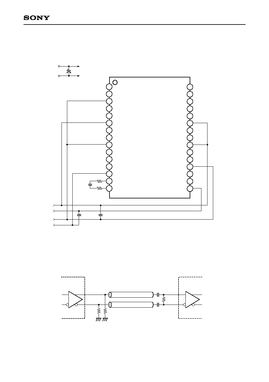
Application Circuit
1. Power and loop filter
200
200
0.022
µ
F
0.1
µ
F
0.1
µ
F
V
CC
V
CC
V
EE
V
EE
22
µ
F
3.3V
GND
1
2
3
4
5
6
7
8
9
10
11
12
13
14
15
REFCLK
LKDT
V
EE
T
DIAG_OUT
DIAG_OUTN
V
CC
E
LOOP_IN
LOOP_INN
V
EE
G
PORT_IN
PORT_INN
LKREFN
V
EE
P
LPF1
LPF2
16
17
18
19
20
21
22
23
24
25
26
27
28
29
30
CDR_SELN
DIAG_SELN
LOOP_SELN
DIAG_IN
DIAG_INN
V
CC
G
LOOP_OUT
LOOP_OUTN
V
CC
E
PORT_OUT
PORT_OUTN
V
EE
E
PORT_SEL0N
PORT_SEL1N
V
CC
P
Application circuits shown are typical examples illustrating the operation of the devices. Sony cannot assume responsibility for
any problems arising out of the use of these circuits or for any infringement of third party patent and other right due to same.
Application circuits shown are typical examples illustrating the operation of the devices. Sony cannot assume responsibility for
any problems arising out of the use of these circuits or for any infringement of third party patent and other right due to same.
0.01
µ
F
0.01
µ
F
150
150
Z
O
= 75
V
CC
= 3.3V
V
EE
= GND
CXB1595AN output
CXB1595AN input
150
2. Serial input and output
≠ 11 ≠
CXB1595AN
Description of Operation
1. Clock and data recovery
The PLL in the clock and data recovery block must be frequency locked to the external REFCLK before locking
to the data.
The LKREFN pin is used to lock the frequency. When the LKREFN pin is low, the PLL frequency is locked to
the external REFCLK and when high, it is locked to the input serial data. Up to 800µs is required to lock the
frequency.
2. Frequency detector
The frequency detector constantly monitors the offset between the clock obtained by 1/20 frequency-dividing
the recovered clock and the external REFCLK. It outputs high when this offset is less than 1.6%, and low when
this offset is 1.6% or more.
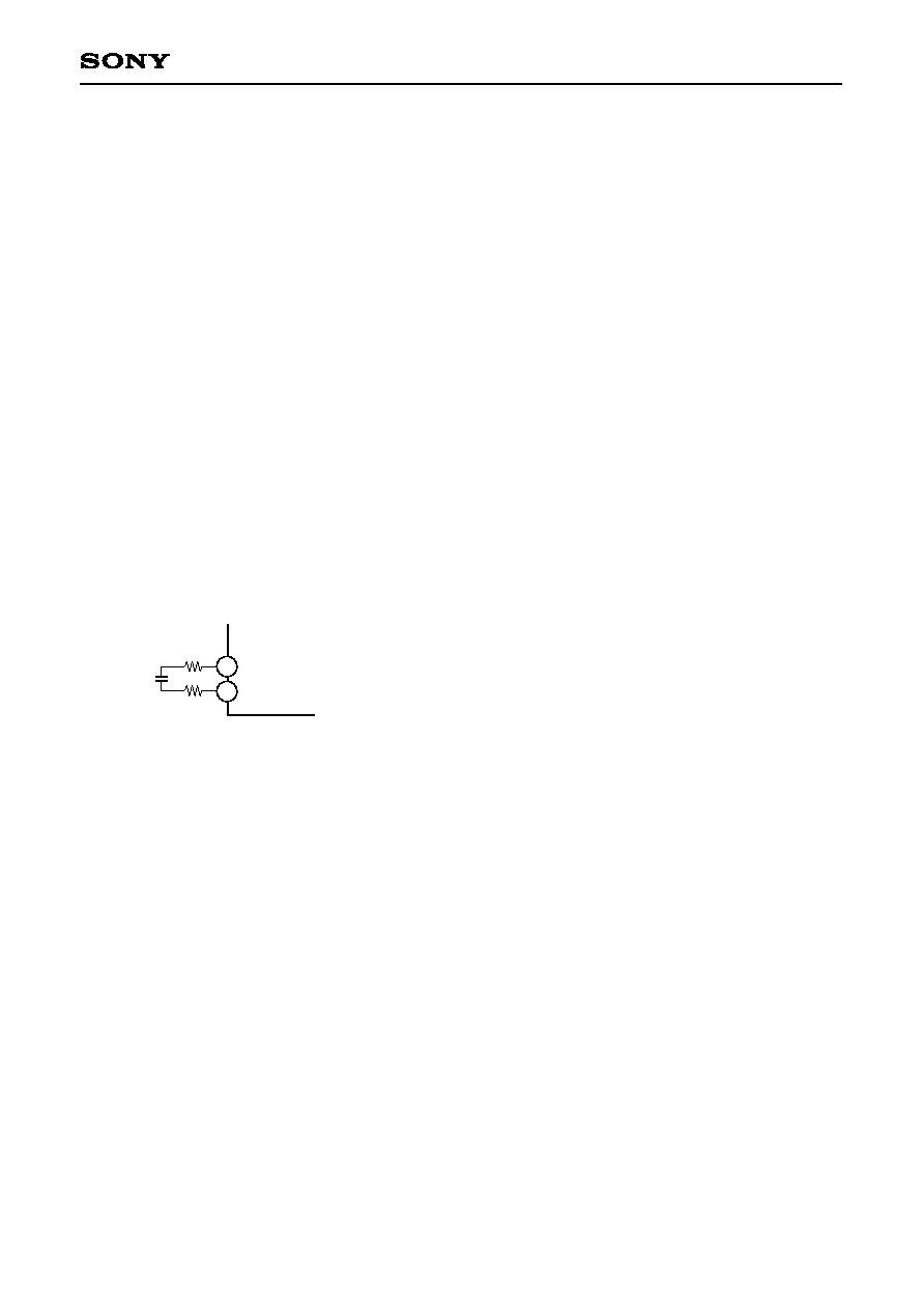
Note on Operation
The following values are recommended for the external resistors and capacitor used as the loop filter.
200
200
0.022
µ
F
14
15

≠ 12 ≠
CXB1595AN
5
0
≠5
≠10
≠15
≠20
100
1000
10
4
Frequency [Hz]
J
i
t
t
e
r
r
a
t
i
o
[
d
B
]
10
5
Jitter Transfer
10
6
10
7
Input data = 00110011...
Loop filter resistor = 200
Loop filter capacitor = 0.022
µ
F
Example of Jitter Transfer Measurement

≠ 13 ≠
CXB1595AN
PORT-OUT Output Eye Pattern
(1.0625Gbps Retimed data)
Example of Random Jitter Measurement
X: 200ps/div
Y: 200mV/div
X: 100ps/div
Y: 200mV/div
Input data = 010101...
Random Jitter = 9.1ps (rms)
Example of Representative Characteristics

≠ 14 ≠
CXB1595AN
Package Outline
Unit: mm
SONY CODE
EIAJ CODE
JEDEC CODE
PACKAGE STRUCTURE
PACKAGE MATERIAL
LEAD TREATMENT
LEAD MATERIAL
PACKAGE MASS
EPOXY RESIN
SOLDER/PALLADIUM
42/COPPER ALLOY
30PIN SSOP (PLASTIC)
9.7 ± 0.1
5
.
6
±
0
.
1
0.65
b
30
1
15
16
1.25
+ 0.2
≠ 0.1
7
.
6
±
0
.
2
A
SSOP-30P-L01
SSOP030-P-0056
0.1g
0.1 ± 0.1
0
.
5
±
0
.
2
0∞ to 10∞
DETAIL A
PLATING
0.10
0.13 M
NOTE: Dimension "
" does not include mold protrusion.
b=0.22 ≠ 0.05
+ 0.1
0
.
1
5
≠
0
.
0
2
+
0
.
0
5
(0.22)
(
0
.
1
5
)
0
.
1
5
≠
0
.
0
1
DETAIL B : SOLDER
DETAIL B : PALLADIUM
+
0
.
0
3
b=0.22 ± 0.03