 | –≠–ª–µ–∫—Ç—Ä–æ–Ω–Ω—ã–π –∫–æ–º–ø–æ–Ω–µ–Ω—Ç: CXD1818 | –°–∫–∞—á–∞—Ç—å:  PDF PDF  ZIP ZIP |
≠ 1 ≠
CXD1818R
E97528-PS
CD-ROM Decoder
Description
The CXD1818R is a CD-ROM decoder LSI with a
built-in Fast SCSI controller. This supports 32
◊
speed
playback.
Features
∑ Ultra SCSI controller (Target mode)
∑ Maximum transfer speed of 20MB/s (when using
Ultra SCSI synchronous transfer)
∑ SCSI overhead reduced by executing multiple
SCSI sequences
∑ Supports SCAM Level 2
∑ Compatible with CD-ROM, CD-I and CD-ROM XA
formats
∑ Real-time error correction
∑ Capable of handling up to 32
◊
speed playback
∑ Multiblock auto-transfer function
∑ Can read subcode-Q data for each byte from the
sub CPU
∑ Real-time subcode (R to W) error correction
∑ Serial transfer of commands to CD DSP
∑ Connectable with standard DRAM of up to 8M bits
(1024K bytes)
∑ DRAM bit width selectable for 8 bits or 16 bits
∑ ESP function
Absolute Maximum Ratings (Ta = 25∞C)
∑ Supply voltage
V
DD
≠0.5 to +7.0
V
∑ Input voltage
V
I
≠0.5 to V
DD
+ 0.5
V
∑ Output voltage
V
O
≠0.5 to V
DD
+ 0.5
V
∑ Operating temperature Topr
≠20 to +75
∞C
∑ Storage temperature
Tstg
≠55 to +150
∞C
Recommended Operating Conditions
∑ Supply voltage
V
DD
4.5 to 5.5 (5.0 typ.) V
∑ Operating temperature Topr
≠20 to +75
∞C
∑ Crystal oscillation
X'tal
40
MHz
Applications
CD-ROM drives
Structure
Silicon gate CMOS IC
Sony reserves the right to change products and specifications without prior notice. This information does not convey any license by
any implication or otherwise under any patents or other right. Application circuits shown, if any, are typical examples illustrating the
operation of the devices. Sony cannot assume responsibility for any problems arising out of the use of these circuits.
144 pin LQFP (Plastic)
For the availability of this product, please contact the sales office.
≠ 2 ≠
CXD1818R
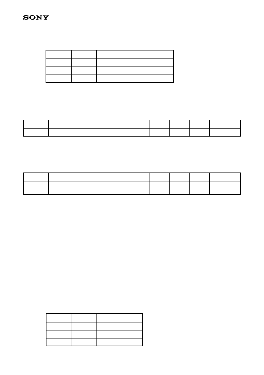
Connection Example
Address
Decoder
sub CPU
CPU data bus
CPU address bus
8bit
7bit
16bit
10bit
SCSI Bus
XATN
XBSY
XACK
XRST
XSEL
XMSG
XCD
XREQ
XIO
XDBP,
XDB (7:0)
EXCK
SBIN
SCOR
WFCK
C2PO
BCLK
MDAT
LRCK
XLAT
DATO
DSTB
A (6:0)
XCS XWR XWAT XRD
D (7:0)
INT
MDB
(15:0)
MA
(9:0)
XRAS
XLCAS
XUCAS
XMWR
CXD1818R
CD-ROM Decoder
&
SCSI I/F
CD DSP
Buffer RAM
GRST
DACD
DSPCK
LRCO
BCKO
GSCR
XROF
≠ 3 ≠
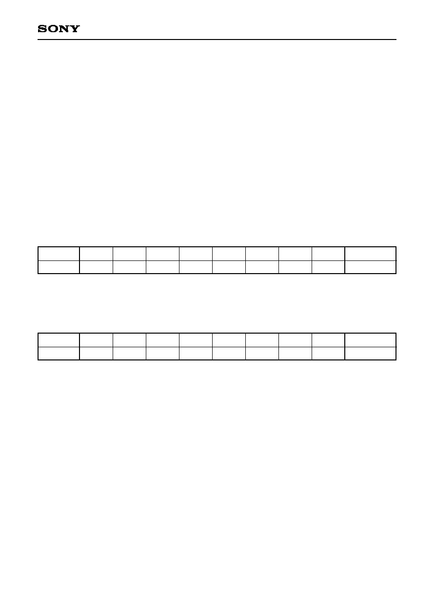
CXD1818R
Block Diagram
65
141 142 143 144
122
123 to 129
131 to 138
54 to 60, 62 to 64
71 to 78, 80 to 87
3
∑
5
∑
8
∑
10
∑
11
∑
15
∑
17
∑
19
∑
22
CD-ROM Decoder Block
SCSI Controller Block
sub CPU
I/F
Descrambler
Sync Control
Priority Resolver
FIFO Control
16byte FIFO
24bit Transfer Byte Counter
Microcode
ROM
Microcode
Core
&
Registers
Arbitration
Selection
SCSI
Phase Ctrl
SCSI
Handshake
Buffer
Handshake
Buffer
Address Gen.
DMA
Sequencer
Subcode
Deinterleave & ECC
Main Data
Error Correction
CD DSP
I/F
MA (0:9)
MDB (0:15)
XMWR
XUCAS
XLCAS
XRAS
EXCK
SBIN
SCOR
WFCK
C2PO
BCLK
MDAT
LRCK
DSPCK
GSCR
DATO
XDB (0:7)
XDBP
XREQ
XACK
XRST
XBSY
XATN
XSEL
XCD
XMSG
XIO
D (7:0)
A (0:6)
XWAT
XTL2
CLK
XTL1
XRES
XCS
XWR
INT
XRD
101
102
103
106
107
108
109
90
91
92
93
94
95
96
97
99
100
110
XLAT
DSTB
BCKO
DACD
LRCO
GRST
XROF
66
67
68
41
29
30
26
24
36
39
35
43
VCO
44
45
48
49
50
53
Clock
Gen.
CM1
AC

≠ 4 ≠
CXD1818R
Pin Configuration
36
35
34
31 32 33
2
3
4
5
6
7
8
9
10 11 12 13 14 15 16 17 18 19 20 21 22 23 24 25 26 27 28 29 30
1
40
39
38
37
41
42
43
44
45
46
47
48
49
50
51
52
53
54
55
56
57
58
59
60
70
69
68
67
63
64
65
66
61
62
71
72
97 96 95 94
91
92
93
100 99 98
101
102
103
104
105
106
107
108
73
74
81
82
83
84
75
76
77
78
88 87 86 85
79
80
89
90
111
109
110
112
113
114
115
116
117
118
119
120
121
122
123
124
125
126
127
128
129
130
131
132
133
134
135
136
137
138
139
140
141
142
143
144
MA4
MA3
MA2
MA1
MA0
XRES
V
DD
V
SS
XTL1
XTL2
AV
DD
AV
SS
AC
CM1
XIO
V
SS
XREQ
V
SS
V
SS
V
DD
XDB0
V
DD
XDB2
V
SS
XDB3
XDB4
V
SS
V
SS
V
DD
XDB5
V
SS
XDB6
V
SS
XDB7
V
SS
V
DD
XDBP
V
SS
XATN
V
SS
XBSY
V
SS
XACK
XRST
V
SS
V
SS
V
DD
TST1
TST2
TST3
V
SS
TST4
TST5
TST6
TST7
V
SS
V
DD
XWAT
A0
A1
A2
A3
A4
A5
A6
V
SS
D0
D1
D2
D3
D4
D5
D6
D7
V
SS
V
DD
INT
XCS
XWR
XRD
TST0
LRCO
DACD
V
DD
V
SS
DSTB
XLAT
GSCR
DSPCK
MDB6
V
SS
LRCK
MDAT
BCLK
C2PO
WFCK
SCOR
V
DD
V
SS
MDB15
MDB14
MDB13
MDB12
MDB11
MDB10
MDB8
V
SS
MDB7
MDB5
MDB4
MDB3
XMWR
XLCAS
XUCAS
XRAS
MA9
MA8
MA7
V
SS
MA6
MA5
MDB0
V
DD
V
SS
MDB1
CLK
BCKO
DATO
SBIN
EXCK
MDB9
MDB2
XROF
GRST
XDB1
V
SS
V
SS
V
DD
XCD
V
DD
V
SS
V
SS
XWSG
XSEL

≠ 5 ≠
CXD1818R
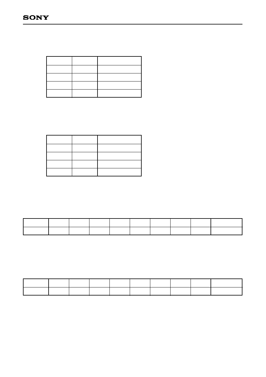
Pin Description
Pin
No.
1
2
3
4
5
6
7
8
9
10
11
12
13
14
15
16
17
18
19
20
21
22
23
24
25
26
27
28
29
30
31
32
33
34
35
36
--
--
I/O
--
I/O
--
--
I/O
--
I/O
I/O
--
--
--
I/O
--
I/O
--
I/O
--
--
I/O
--
I/O
--
I/O
--
--
I/O
I/O
--
--
--
--
I/O
I/O
--
--
Negative
--
Negative
--
--
Negative
--
Negative
Negative
--
--
--
Negative
--
Negative
--
Negative
--
--
Negative
--
Negative
--
Negative
--
--
Negative
Negative
--
--
--
--
Negative
Negative
Power
Power
SCSI I/F
Power
SCSI I/F
Power
Power
SCSI I/F
Power
SCSI I/F
SCSI I/F
Power
Power
Power
SCSI I/F
Power
SCSI I/F
Power
SCSI I/F
Power
Power
SCSI I/F
Power
SCSI I/F
Power
SCSI I/F
Power
Power
SCSI I/F
SCSI I/F
Power
Power
Power
Power
SCSI I/F
SCSI I/F
V
SS
V
DD
SCSI data bus bit 0
V
SS
SCSI data bus bit 1
V
SS
V
DD
SCSI data bus bit 2
V
SS
SCSI data bus bit 3
SCSI data bus bit 4
V
SS
V
SS
V
DD
SCSI data bus bit 5
V
SS
SCSI data bus bit 6
V
SS
SCSI data bus bit 7
V
SS
V
DD
SCSI data bus parity
V
SS
SCSI control bus XATN signal
V
SS
SCSI control bus XBSY signal
V
SS
V
DD
SCSI control bus XACK signal
SCSI control bus XRST signal
V
SS
V
SS
V
DD
V
SS
SCSI control bus XMSG signal
SCSI control bus XSEL signal
V
SS
V
DD
XDB0
V
SS
XDB1
V
SS
V
DD
XDB2
V
SS
XDB3
XDB4
V
SS
V
SS
V
DD
XDB5
V
SS
XDB6
V
SS
XDB7
V
SS
V
DD
XDBP
V
SS
XATN
V
SS
XBSY
V
SS
V
DD
XACK
XRST
V
SS
V
SS
V
DD
V
SS
XMSG
XSEL
Symbol
I/O
Logic
Classification
Description

≠ 6 ≠
CXD1818R
37
38
39
40
41
42
43
44
45
46
47
48
49
50
51
52
53
54
55
56
57
58
59
60
61
62
63
64
65
66
67
68
69
70
71
72
73
--
--
I/O
--
I/O
--
I/O
O
I
--
--
O
I
O
--
--
I
O
O
O
O
O
O
O
--
O
O
O
O
O
O
O
--
--
I/O
I/O
I/O
--
--
Negative
--
Negative
--
Negative
--
--
--
--
Negative
--
Negative
Negative
Negative
Negative
--
--
Power
Power
SCSI I/F
Power
SCSI I/F
Power
SCSI I/F
VCO Charge Pump Out
VCO Control
Analog Power
Analog Power
System I/F
System I/F
System I/F
Power
Power
System I/F
BufMem I/F
BufMem I/F
BufMem I/F
BufMem I/F
BufMem I/F
BufMem I/F
BufMem I/F
Power
BufMem I/F
BufMem I/F
BufMem I/F
BufMem I/F
BufMem I/F
BufMem I/F
BufMem I/F
Power
Power
BufMem I/F
BufMem I/F
BufMem I/F
V
SS
V
DD
SCSI control bus XCD signal
V
SS
SCSI control bus XREQ signal
V
SS
SCSI control bus XIO signal
Multiplier VCO charge pump output
Multiplier VCO control voltage input
Analog V
SS
Analog V
DD
Crystal oscillation circuit output
Crystal oscillation circuit input
Clock output
V
SS
V
DD
CXD1818R reset signal
Address bus output bit 0 to buffer memory
Address bus output bit 1 to buffer memory
Address bus output bit 2 to buffer memory
Address bus output bit 3 to buffer memory
Address bus output bit 4 to buffer memory
Address bus output bit 5 to buffer memory
Address bus output bit 6 to buffer memory
V
SS
Address bus output bit 7 to buffer memory
Address bus output bit 8 to buffer memory
Address bus output bit 9 to buffer memory
Buffer memory RAS (Row Address Strobe) signal
Buffer memory CAS (Column Address Strobe) signal
Buffer memory CAS (Column Address Strobe) signal
Data write strobe signal to buffer memory
V
SS
V
DD
Buffer memory data bus bit 0
Buffer memory data bus bit 1
Buffer memory data bus bit 2
V
SS
V
DD
XCD
V
SS
XREQ
V
SS
XIO
CM1
AC
AV
SS
AV
DD
XTL2
XTL1
CLK
V
SS
V
DD
XRES
MA0
MA1
MA2
MA3
MA4
MA5
MA6
V
SS
MA7
MA8
MA9
XRAS
XUCAS
XLCAS
XMWR
V
SS
V
DD
MDB0
MDB1
MDB2
Pin
No.
Symbol
I/O
Logic
Classification
Description

≠ 7 ≠
CXD1818R
74
75
76
77
78
79
80
81
82
83
84
85
86
87
88
89
90
91
92
93
94
95
96
97
98
99
100
101
102
103
104
105
106
107
I/O
I/O
I/O
I/O
I/O
--
I/O
I/O
I/O
I/O
I/O
I/O
I/O
I/O
--
--
O
I
I
I
I
I
I
I
--
I
I
O
O
O
--
--
O
O
--
--
--
--
--
--
BufMem I/F
BufMem I/F
BufMem I/F
BufMem I/F
BufMem I/F
Power
BufMem I/F
BufMem I/F
BufMem I/F
BufMem I/F
BufMem I/F
BufMem I/F
BufMem I/F
BufMem I/F
Power
Power
CD DSP I/F
CD DSP I/F
CD DSP I/F
CD DSP I/F
CD DSP I/F
CD DSP I/F
CD DSP I/F
CD DSP I/F
Power
CD DSP I/F
CD DSP I/F
CD DSP I/F
CD DSP I/F
CD DSP I/F
Power
Power
CD DSP I/F
CD DSP I/F
Buffer memory data bus bit 3
Buffer memory data bus bit 4
Buffer memory data bus bit 5
Buffer memory data bus bit 6
Buffer memory data bus bit 7
V
SS
Buffer memory data bus bit 8
Buffer memory data bus bit 9
Buffer memory data bus bit 10
Buffer memory data bus bit 11
Buffer memory data bus bit 12
Buffer memory data bus bit 13
Buffer memory data bus bit 14
Buffer memory data bus bit 15
V
SS
V
DD
SBIN readout clock
(connected to the EXCK pin (Pin 65) of the CXD3000)
Subcode serial signal
(connected to the SBSO pin (Pin 64) of the CXD3000)
Subcode sync signal
(connected to the SCOR pin (Pin 63) of the CXD3000)
Write frame clock
(connected to the WFCK pin (Pin 62) of the CXD3000)
C2 pointer signal. Indicates that an error exists in MDAT.
Bit clock. MDAT strobe signal
Serial data stream from CD DSP
LR signal. Indicates MDAT left or right channel
V
SS
DSP crystal input
SCOR synchronized with DSP data output
(connected to the GRSCOR pin (Pin 113) of the CXD3000)
Serial data output from sub CPU to CD DSP
DATO latch signal. Latched at the rising edge.
DATO transfer clock
V
SS
V
DD
Bit clock
(connected to the BCKI pin (Pin 30) of the CXD3000)
Audio data output to DAC
(connected to the PCMDI pin (Pin 28) of the CXD3000)
MDB3
MDB4
MDB5
MDB6
MDB7
V
SS
MDB8
MDB9
MDB10
MDB11
MDB12
MDB13
MDB14
MDB15
V
SS
V
DD
EXCK
SBIN
SCOR
WFCK
C2PO
BCLK
MDAT
LRCK
V
SS
DSPCK
GSCR
DATO
XLAT
DSTB
V
SS
V
DD
BCKO
DACD
Pin
No.
Symbol
I/O
Logic
Classification
Description

≠ 8 ≠
CXD1818R
108
109
110
111
112
113
114
115
116
117
118
119
120
121
122
123
124
125
126
127
128
129
130
131
132
133
134
135
136
137
138
139
140
141
142
143
144
O
O
I
I
I
I
I
--
I
I
I
I
--
--
O
I
I
I
I
I
I
I
--
I/O
I/O
I/O
I/O
I/O
I/O
I/O
I/O
--
--
O
I
I
I
Negative
--
--
--
Negative
--
--
--
Selectable
Negative
Negative
Negative
CD DSP I/F
CD DSP I/F
CD DSP I/F
Test I/F
Test I/F
Test I/F
Test I/F
Power
Test I/F
Test I/F
Test I/F
Test I/F
Power
Power
sub CPU I/F
sub CPU I/F
sub CPU I/F
sub CPU I/F
sub CPU I/F
sub CPU I/F
sub CPU I/F
sub CPU I/F
Power
sub CPU I/F
sub CPU I/F
sub CPU I/F
sub CPU I/F
sub CPU I/F
sub CPU I/F
sub CPU I/F
sub CPU I/F
Power
Power
sub CPU I/F
sub CPU I/F
sub CPU I/F
sub CPU I/F
LR clock output to DAC
(connected to the LRCKI pin (Pin 26) of the CXD3000)
GRSCOR resynchronization output
(connected to the SCSY pin (Pin 68) of the CXD3000)
DSP RAM overflow input
(connected to the XROF pin (Pin 45) of the CXD3000)
Test pin 0
Test pin 1
Test pin 2
Test pin 3
V
SS
Test pin 4
Test pin 5
Test pin 6
Test pin 7
V
SS
V
SS
Wait signal for sub CPU buffer memory access
CXD1818R built-in register address bus bit 0
CXD1818R built-in register address bus bit 1
CXD1818R built-in register address bus bit 2
CXD1818R built-in register address bus bit 3
CXD1818R built-in register address bus bit 4
CXD1818R built-in register address bus bit 5
CXD1818R built-in register address bus bit 6
V
SS
Sub CPU data bus bit 0
Sub CPU data bus bit 1
Sub CPU data bus bit 2
Sub CPU data bus bit 3
Sub CPU data bus bit 4
Sub CPU data bus bit 5
Sub CPU data bus bit 6
Sub CPU data bus bit 7
V
SS
V
DD
Interrupt to sub CPU
CXD1818R chip select signal
CXD1818R built-in register write signal
CXD1818R built-in register read signal
LRCO
GRST
XROF
TST0
TST1
TST2
TST3
V
SS
TST4
TST5
TST6
TST7
V
SS
V
SS
XWAT
A0
A1
A2
A3
A4
A5
A6
V
SS
D0
D1
D2
D3
D4
D5
D6
D7
V
SS
V
DD
INT
XCS
XWR
XRD
Pin
No.
Symbol
I/O
Logic
Classification
Description

≠ 9 ≠
CXD1818R
Electrical Characteristics
(V
DD
= 5V ± 10%, V
SS
= 0V, Topr = ≠20 to +75∞C)
Item
TTL input level pin
High level input voltage
TTL input level pin
Low level input voltage
CMOS input level pin
High level input voltage
CMOS input level pin
Low level input voltage
CMOS Schmitt input level pin
High level input voltage
CMOS Schmitt input level pin
Low level input voltage
CMOS Schmitt input level pin
Input voltage hysteresis
TTL Schmitt input level pin
High level input voltage
TTL Schmitt input level pin
Low level input voltage
TTL Schmitt input level pin
Input voltage hysteresis
SCSI Schmitt input level pin
High level input voltage
SCSI Schmitt input level pin
Low level input voltage
SCSI Schmitt input level pin
Input voltage hysteresis
Bidirectional pin with pull-up resistor
Input current
Input voltage
High level output voltage
High level output voltage
SCSI high level output voltage
Low level output voltage
SCSI low level output voltage
Input leakage current
Oscillation cell high level input voltage
Oscillation cell low level input voltage
Oscillation cell logic threshold value
Oscillation cell feedback resistance value
Oscillation cell high level output voltage
Oscillation cell low level output voltage
V
IH1
V
IL1
V
IH2
V
IL2
V
IH4
V
IL4
V
IH4
≠ V
IL4
V
IH5
V
IL5
V
IH5
≠ V
IL4
V
IHS
V
ILS
V
IHTS
≠ V
ILTS
I
IL3
V
IN6
V
OH1
V
OH2
V
OHS
V
OL1
V
OLS
I
I1
V
IH4
V
IL4
LV
TH
R
FB
V
OH3
V
OL3
V
IN
= 0V
Analog input
I
OH
= ≠2mA
I
OH
= ≠6mA
I
OL
= 4mA
I
OL
= 48mA
V
IN
= V
SS
or V
DD
V
IN
= V
SS
or V
DD
I
OH
= ≠12mA
I
OL
= 12mA
2.2
0.7V
DD
0.8V
DD
2.2V
2.2V
≠40
V
SS
V
DD
≠ 0.8
V
DD
≠ 0.8
2.5
≠10
0.7V
DD
250k
0.5V
DD
0.6
0.4
0.4
≠100
0.5V
DD
1M
0.8
0.3V
DD
0.2V
DD
0.8V
0.8V
≠240
V
DD
3.7
0.4
0.5
10
0.3V
DD
2.5M
0.5V
DD
V
V
V
V
V
V
V
V
V
V
V
V
V
µA
V
V
V
V
V
V
µA
V
V
V
V
V
1
1
2
2
3
3
3
4
4
4
11
11
11
5
13
6
7
12
8
11
9
10
Symbol
Conditions
Min.
Typ.
Max.
Unit
Applicable
pins
≠ 10 ≠
CXD1818R
1
D7 to 0, MDBF to 0, MDAT, LRCK, C2PO, SBIN, SCOR, WFCK, XROF
2
GRST, DACD, LRCK, BCKO, TST7 to 0
3
XRES
4
A6 to 0, XWR, XRD, XCS, BCLK, DSPCK, GSCR
5
D7 to 0, MDBF to 0
6
All output pins except XTL2, XRAS, XUCAS, XLCAS, XMWR and CLK
7
XRAS, XUCAS, XLCAS, XMWR, CLK, CM1
8
All output pins except XTL2
9
All input pins except
5
and XTL1
10
Input: XTL1, Output: XTL2
11
XRST, XBSY, XSEL, XATN, XMSG, XCD, XIO, XREQ, XACK, XDBP, XDB7 to 0
12
XREQ, XACK, XDBP and XDB7 to 0 when active negation is ON
13
AC
I/O Capacitance
(V
DD
= V
I
= 0V, f = 1MHz)
Item
Input capacitance
Output capacitance
I/O capacitance
C
IN
C
OUT
C
I/O
9
11
11
pF
pF
pF
Symbol
Min.
Typ.
Max.
Unit
≠ 11 ≠
CXD1818R
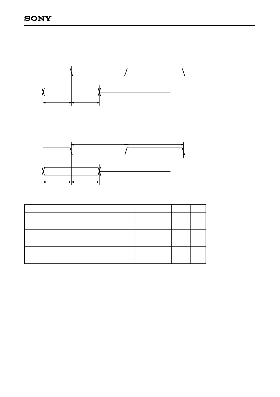
AC Characteristics
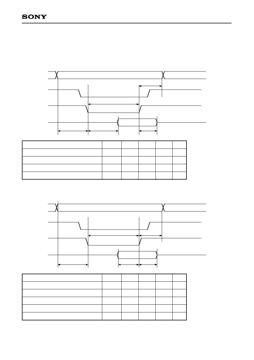
1. Sub CPU Interface (Output Load = 50pF)
(1) Read
Tsar
Thar
A6 to 0
XCS
XRD
D7 to 0
Tdrd
Tfrd
Trrl
Item
Address setup time (for XCS & XRD
)
Address hold time (for XCS & XRD
)
Data delay time (for XCS & XRD
)
Data float time (for XCS & XRD
)
Tsar
Thar
Tdrd
Tfrd
10
10
0
35
15
ns
ns
ns
ns
Symbol
Min.
Typ.
Max.
Unit
Tsaw
Thwa
A6 to 0
XCS
XWR
D7 to 0
Tsdw
Thdw
Twwl
Item
Address setup time (for XCS & XWR
)
Address hold time (for XCS & XWR
)
Data setup time (for XCS & XWR
)
Data hold time (for XCS & XWR
)
Low level XWR pulse width
Tsaw
Thaw
Tsdw
Thdw
Twwl
20
10
20
10
30
ns
ns
ns
ns
ns
Symbol
Min.
Typ.
Max.
Unit
(2) Write
≠ 12 ≠
CXD1818R
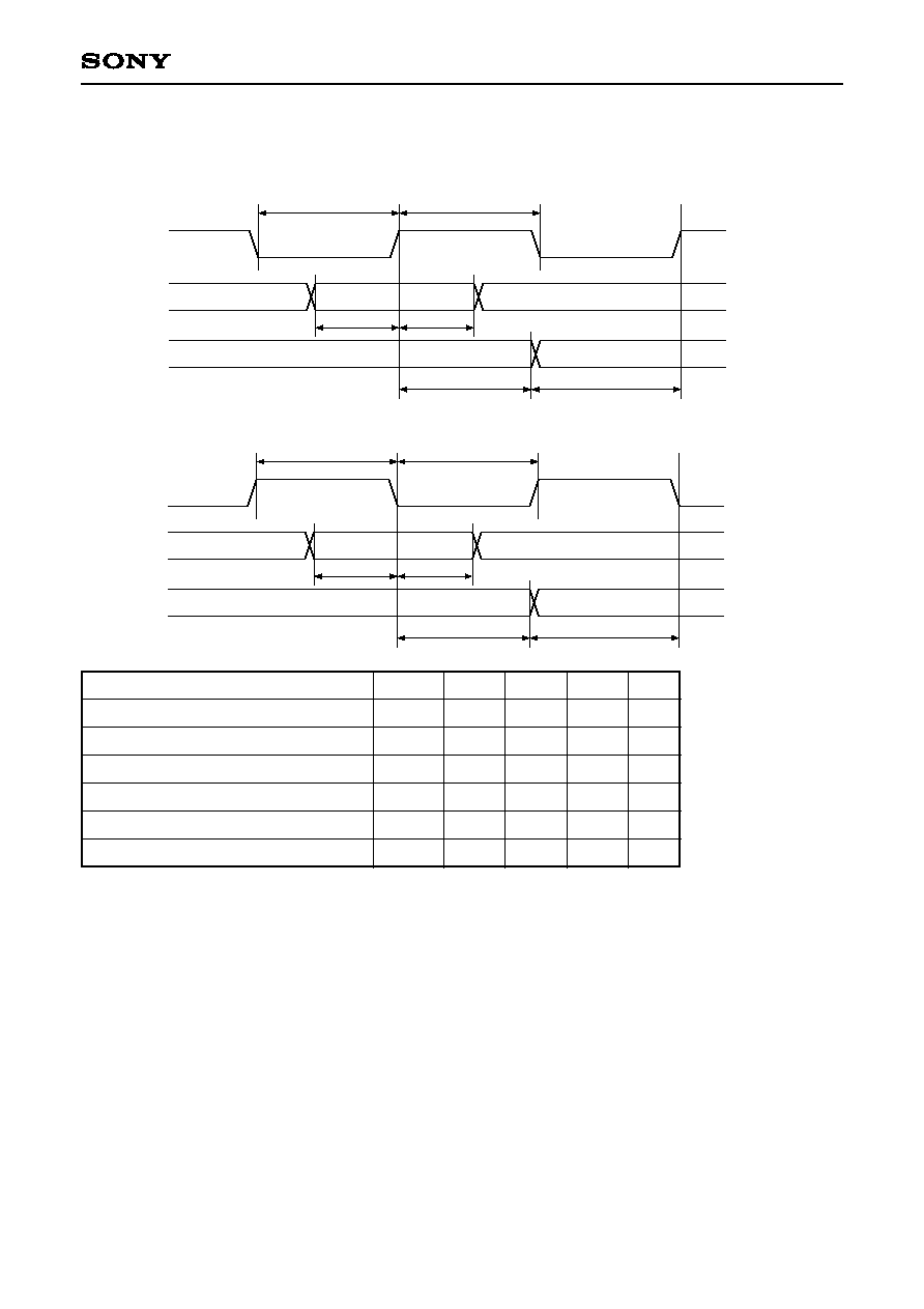
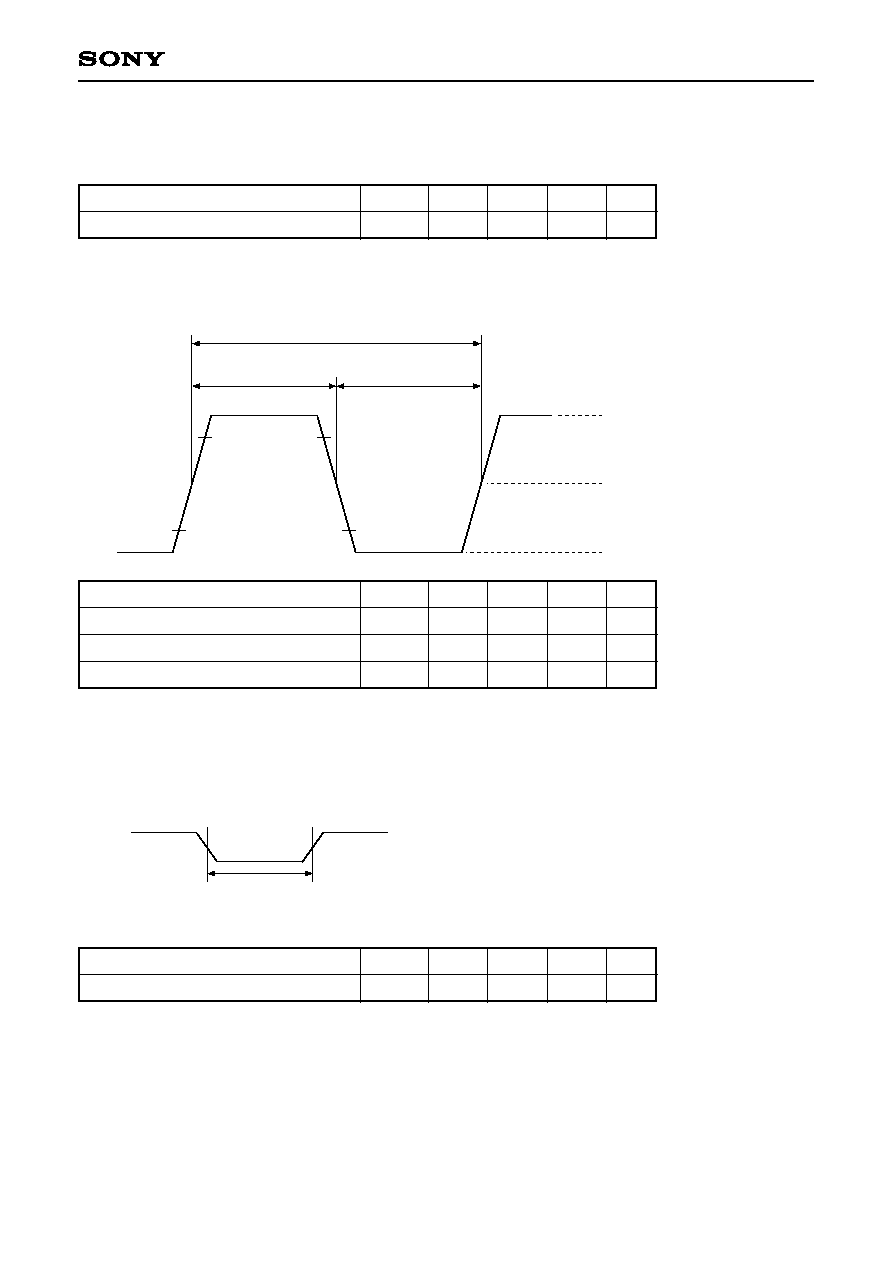
2. CD DSP Interface
BCKRED = "H"
Tbck
Tbck
Tsb1
Thb1
Tsb2
Thb2
BCLK
DATA
LRCK
C2PO
BCKRED = "L"
Tbck
Tbck
Tsb1
Thb1
Tsb2
Thb2
BCLK
DATA
LRCK
C2PO
Item
BCLK frequency
BCLK pulse width
DATA setup time (for BCLK)
DATA hold time (for BCLK)
LRCK, C2PO setup time (for BCLK)
LRCK, C2PO hold time (for BCLK)
Fbck
Tbck
Tsb1
Thb1
Tsb2
Thb2
19
10
10
10
10
26
MHz
ns
ns
ns
ns
ns
Symbol
Min.
Typ.
Max.
Unit
≠ 13 ≠
CXD1818R
3. DRAM Interface (Output Load = 30pF)
(1) Read
Tma0
iCLK
Tma1
Trasl
Trash
Trc
Tcasl
Tcash
Tmdrs
Tmdrh
"H"
MA9 to 0
XRAS
XUCAS
XLCAS
XMWR
MDBF to 0
Item
Random read/write cycle time
Address delay time (for XTL2
)
Address delay time (for XTL2
)
XRAS
delay time (for XTL2
)
XRAS
delay time (for XTL2
)
XCAS
delay time (for XTL2
)
XCAS
delay time (for XTL2
)
Data setup time (for XTL2
)
Data hold time (for XCAS
)
Trc
Tma0
Tma1
Trasl
Trash
Tcasl
Tcash
Tmdrs
Tmdrh
5Tw
13
11
6
6
7
6
2
0
24
22
12
11
14
12
4
45
41
23
20
25
22
6
ns
ns
ns
ns
ns
ns
ns
ns
ns
Symbol
Min.
Typ.
Max.
Unit
≠ 14 ≠
CXD1818R
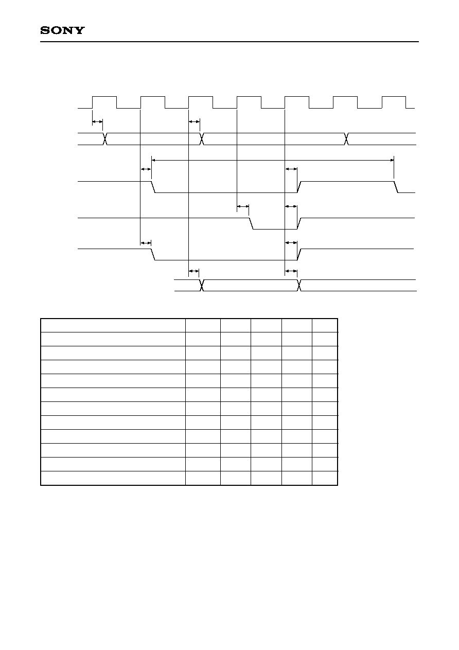
(2) Write
Tma0
iCLK
Tma1
Trasl
Trash
Trc
Tcash
Tcasl
Tmdws
MA9 to 0
XRAS
XUCAS
XLCAS
XMWR
MDBF to 0
Tmwrh
Tmwrl
Tmdwh
Item
Random read/write cycle time
Address delay time (for XTL2
)
Address delay time (for XTL2
)
XRAS
delay time (for XTL2
)
XRAS
delay time (for XTL2
)
XCAS
delay time (for XTL2
)
XCAS
delay time (for XTL2
)
XMWR
delay time (for XTL2
)
XMWR
delay time (for XTL2
)
Data setup time (for XTL2
)
Data hold time (for XTL2
)
Trc
Tma0
Tma1
Trasl
Trash
Tcasl
Tcash
Tmwrl
Tmwrh
Tmdws
Tmdwh
5Tw
13
11
6
6
7
6
7
6
14
7
24
22
12
11
14
12
14
11
28
14
45
41
23
20
25
22
25
21
51
26
ns
ns
ns
ns
ns
ns
ns
ns
ns
ns
ns
Symbol
Min.
Typ.
Max.
Unit
≠ 15 ≠
CXD1818R
(3) Refresh (RAS only refresh)
Tma0
iCLK
Trasl
Trash
MA9 to 0
XRAS
XUCAS
XLCAS
XMWR
"H"
"H"
Item
Random read/write cycle time
Address delay time (for XTL2
)
XRAS
delay time (for XTL2
)
XRAS
delay time (for XTL2
)
Trc
Tma0
Trasl
Trash
5Tw
12
6
6
24
12
11
43
23
20
ns
ns
ns
ns
Symbol
Min.
Typ.
Max.
Unit
≠ 16 ≠
CXD1818R
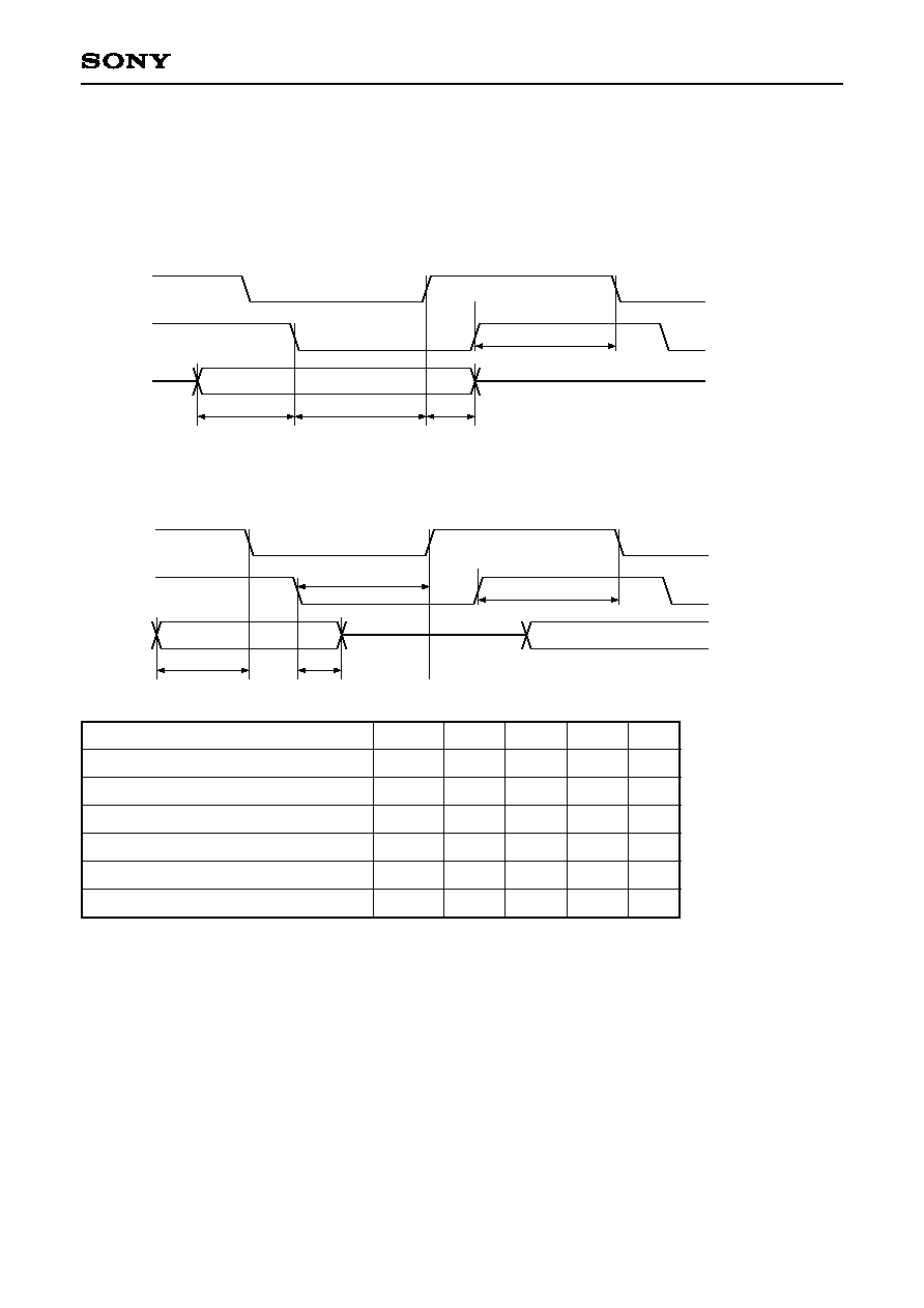
4. SCSI Interface
(1) SCSI asynchronous transfer timing
When receiving: Initiator
Target
Taads
Tardh
XREQ
XACK
XDB
Taaarnd
Taanrad
When transmitting: Target
Initiator
Tards
XREQ
XACK
XDB
Taadh
Taanrad
Taaarnd
Item
XDB setup time (for XACK
)
XDB hold time (for XREQ
)
XDB setup time (for XREQ
)
XDB hold time (for XREQ
)
XREQ rise delay time (for XACK
)
XREQ fall time (for XACK
)
Taads
Tardh
Tards
Taadh
Taaarnd
Taanrad
15
0
30
60
30
30
70
85
ns
ns
ns
ns
ns
ns
Symbol
Min.
Typ.
Max.
Unit
≠ 17 ≠
CXD1818R
(2) SCSI synchronous transfer timing
When receiving: Initiator
Target
Tnads
XACK
XDB
Tnadh
When transmitting: Target
Initiator
Tnrds
XREQ
XDB
Tnrdh
Tnrap
Tnrnp
Item
XDB setup time (for XACK
)
XDB hold time (for XACK
)
XDB setup time (for XREQ
)
XDB hold time (for XREQ
)
XREQ assert time
XREQ negate time
Tnads
Tnadh
Tnrds
Tnrdh
Tnrap
Tnrnp
15
10
80
105
90
110
ns
ns
ns
ns
ns
ns
Symbol
Min.
Typ.
Max.
Unit
≠ 18 ≠
CXD1818R
(3) Fast SCSI synchronous transfer timing
When receiving: Initiator
Target
Tfads
XACK
XDB
Tfadh
When transmitting: Target
Initiator
Tfrds
XREQ
XDB
Tfrdh
Tfrap
Tfrnp
Item
XDB setup time (for XACK
)
XDB hold time (for XACK
)
XDB setup time (for XREQ
)
XDB hold time (for XREQ
)
XREQ assert time
XREQ negate time
Tfads
Tfadh
Tfrds
Tfrdh
Tfrap
Tfrnp
15
10
55
55
40
60
ns
ns
ns
ns
ns
ns
Symbol
Min.
Typ.
Max.
Unit
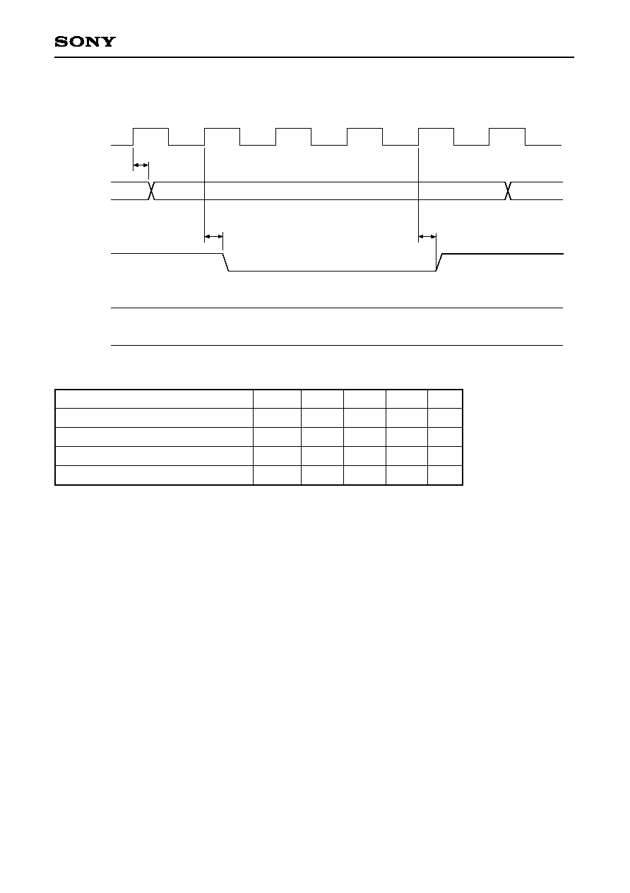
≠ 19 ≠
CXD1818R
(4) SCSI synchronous transfer (Ultra) timing
When receiving: Initiator
Target
Tuads
XACK
XDB
Tuadh
When transmitting: Target
Initiator
Turds
XREQ
XDB
Turdh
Turap
Turnp
Item
XDB setup time (for XACK
)
XDB hold time (for XACK
)
XDB setup time (for XREQ
)
XDB hold time (for XREQ
)
XREQ assert time
XREQ negate time
Tuads
Tuadh
Turds
Turdh
Turap
Turnp
15
10
11.5
16.5
15
30
ns
ns
ns
ns
ns
ns
Symbol
Min.
Typ.
Max.
Unit
≠ 20 ≠
CXD1818R
5. XTL1 and XTL2 Pins
(1) When using self-excited oscillation
Item
Oscillation frequency
Fmax
40.0
MHz
Symbol
Min.
Typ.
Max.
Unit
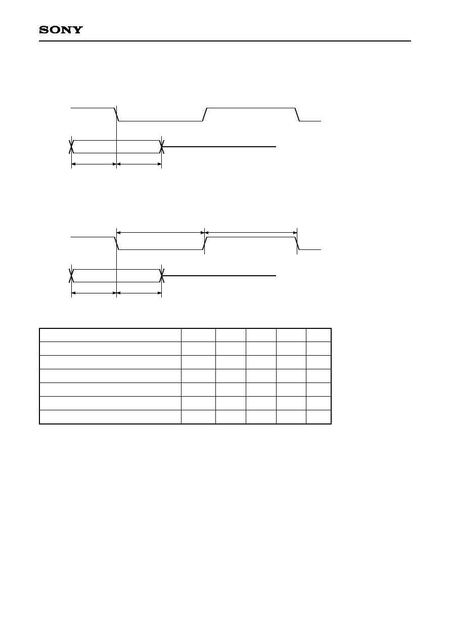
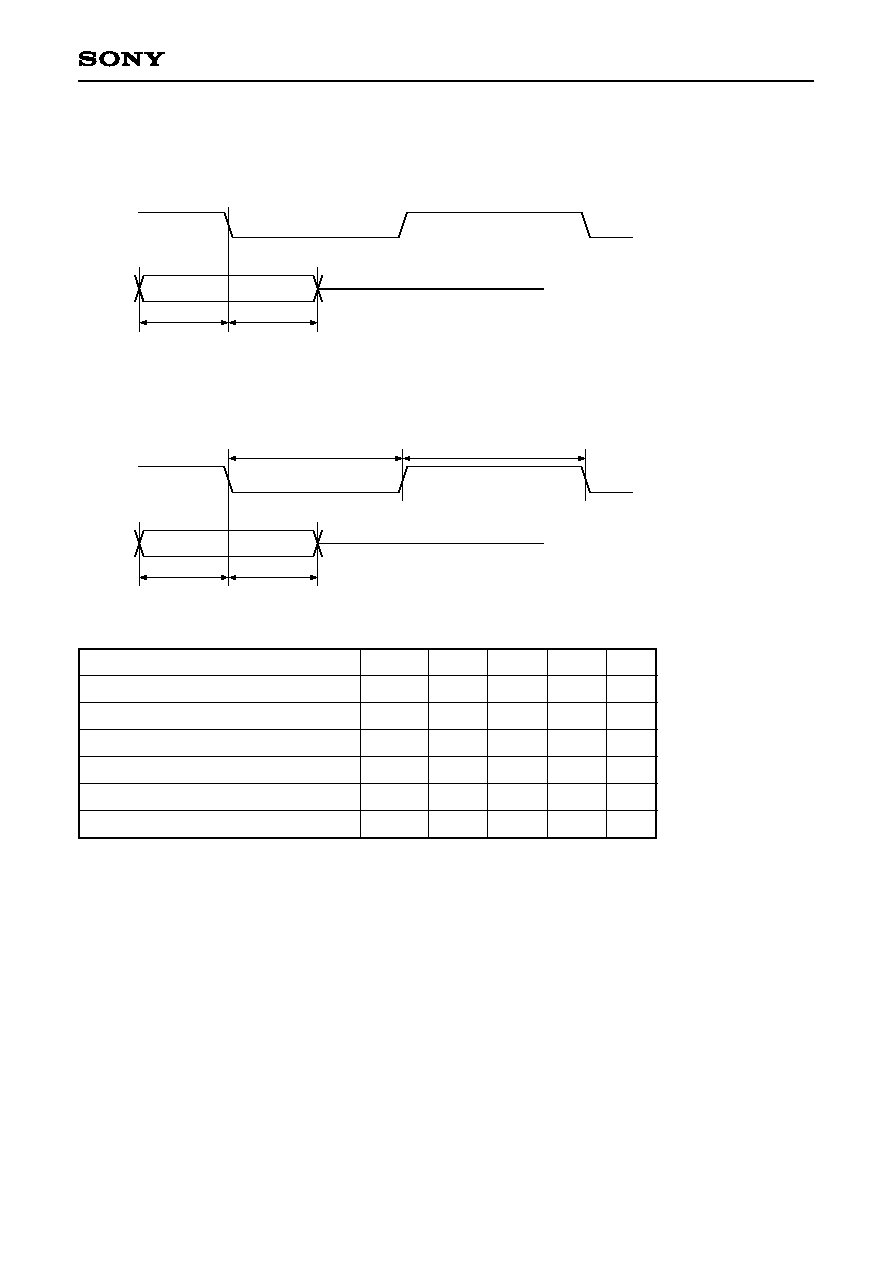
XRES Pin
Reset to IC
Item
XRES "L" hold time
Trs
100
ns
Symbol
Min.
Typ.
Max.
Unit
Vihx
Twlx
Twhx
Tw
V
DD
/2
Vilx
(2) When inputting a pulse to the XTL1 pin
Item
High level pulse width
Low level pulse width
Pulse cycle
Twhx
Twhx
Tw
10
10
25
ns
ns
ns
Symbol
Min.
Typ.
Max.
Unit
Trs

≠ 21 ≠
CXD1818R
Contents
[1] Description of Registers ........................................................................................................................... 22
1-1. Description of Decoder Block Registers ............................................................................................... 22
1-2. Description of SCSI2 Controller Block Registers.................................................................................. 51
1-3. Common Registers ............................................................................................................................... 66
[2] Description of SCSI Controller Block Commands ................................................................................. 77
2-1. Precautions when Executing Commands ............................................................................................. 78
2-2. Category 00 Commands....................................................................................................................... 78
2-3. Category 01 Commands....................................................................................................................... 83
2-4. Category 10 Commands....................................................................................................................... 85
2-5. Category 11 Commands....................................................................................................................... 88
[3] Appendix A................................................................................................................................................. 93
3-1. List of CD-ROM Decoder Block Registers............................................................................................ 93
3-2. List of SCSI Controller Block Registers ................................................................................................ 99
3-3. List of Common Registers .................................................................................................................. 103
3-4. Register Reset Conditions .................................................................................................................. 105
[4] Appendix B............................................................................................................................................... 111
4-1. Summary of SCSI Controller Block Commands ................................................................................. 111
≠ 22 ≠
CXD1818R
[1] Description of Registers
The CXD1818R's register address area is allotted as shown in the table below.
Address
00h to 4Fh
50h to 6Fh
70h to 7Fh
0xx xxxx
100 xxxx
101 xxxx
110 xxxx
111 xxxx
CD-ROM decoder block
SCSI2 interface block
CD-ROM decoder/SCSI2 interface common block
Description
1-1. Description of Decoder Block Registers
1-1-1. 00h
(1) RAWMIN (raw minute) register (read)
RAWMIN (raw minute) register
00h (R)
Adr.
bit7
bit6
bit5
bit4
bit3
bit2
bit1
bit0
Reg.
REWMIN
The Header Minute byte for the sector being sent from the CD DSP while DECINT is active can be read from
this register. A difference of two sectors exists between the RAWxxx and BFxxx registers during the write-only
and real-time correction modes.
(2) CONFIG0 (configuration 0) register (write)
CONFIG0 (configuration 0) register
00h (W)
CINT
POL
RAM
SIZE1
RAM
SIZE0
RAM8
BITW
RAM2
CAS
"L"
CLK
SEL1
CLK
SEL0
Adr.
bit7
bit6
bit5
bit4
bit3
bit2
bit1
bit0
Reg.
CONFIG0
bit 7:
CINTPOL (sub CPU interrupt polarity)
High: The INT pin becomes active high. When the register is inactive, it goes low.
Low: The INT pin becomes active low. When the register is inactive, it goes to high impedance.
bits 6, 5:
RAMSIZE1, 0 (DRAM size 1, 0)
Set these bits according to the total size of the DRAM connected to this IC.
RAMSIZE1
"L"
"L"
"H"
"H"
"L"
"H"
"L"
"H"
1M bits
2M bits
4M bits
8M bits
RAMSIZE0
DRAM total size
bit 4:
RAM8BITW (DRAM 8-bit wide)
This bit is set according to the bit width of the DRAM data bus to be connected.
High: Set this bit high when the DRAM to be connected has the 8-bit width.
Low: Set this bit low when the DRAM to be connected has the 16-bit width.
(Set low when two 8-bit width DRAMs are connected in parallel.)
≠ 23 ≠
CXD1818R
bit 3:
RAM2CAS (DRAM 2 CAS)
When the DRAM bus width is 16 bits, set this bit according to the number of CAS and WE signals.
When the DRAM bus width is 8 bits, this bit has no meaning.
High: Set this bit high when the IC is connected to a DRAM with 2 CAS signals and 1 WE signal.
Low: Set this bit low when the IC is connected to a DRAM with 1 CAS signal and 2 WE signals.
bit 2:
RESERVED
Normally set low.
bits 1, 0:
CLKSEL1, 0 (CLK select 1, 0)
These bits determine the clock frequency output from the CLK pin.
CLKSEL1
"L"
"L"
"H"
"H"
"L"
"H"
"L"
"H"
Fixed to high
Same frequency as XTL1
1/2 of XTL1
RESERVED
CLKSEL0
Clock frequency
1-1-2. 01h
(1) RAWSEC (raw second) register (read)
RAWSEC (raw second) register
01h (R)
Adr.
bit7
bit6
bit5
bit4
bit3
bit2
bit1
bit0
Reg.
RAWSEC
The Header Second byte for the sector being sent from the CD DSP while DECINT is active can be read from
this register.
(2) CONFIG1 (configuration 1) register (write)
CONFIG1 (configuration 1) register
01h (W)
SW
OPEN
SYC
NGC2
SYC
NGC1
SYC
NGC0
DCK
SEL
"L"
SBC
ECC1
SBC
ECC0
Adr.
bit7
bit6
bit5
bit4
bit3
bit2
bit1
bit0
Reg.
CONFIG1
bit 7:
SWOPEN (sync window open)
High: The Sync mark detection window opens. In this case, the IC's internal Sync protection circuit
is disabled.
Low: The Sync mark detection window is controlled by the IC's internal Sync protection circuit.
bits 6 to 4: SYCNGC2 to 0 (sync NG count 2 to 0)
The Sync mark detection window opens once the number of Sync marks specified by these bits is
inserted. Setting a value of 1h or less for these bits is prohibited. (After a reset, these bits are set to
2h.)
bit 3:
DCKSEL (Dsp Clock Select)
High: DSPCLK 16.9344MHz
Low: DSPCLK 33.8688MHz
bit 2:
RESERVED
Normally set low.
≠ 24 ≠
CXD1818R
BCKMD1
"L"
"L"
"H"
"L"
"H"
"X"
16BCLKs/WCLK
24BCLKs/WCLK
32BCLKs/WCLK
BCKMD0
bits 1, 0:
SBCECC1, 0 (subcode ECC 1, 0)
These two bits specify the error correction method when decoding the subcode.
SBECC1
"X"
"L"
"H"
"L"
"H"
"H"
Error correction not performed.
Single error correction performed.
Double error correction performed.
SBECC0
Subcode error correction
1-1-3. 02h
(1) RAWBLK (raw block) register (read)
RAWBLK (raw block) register
02h (R)
Adr.
bit7
bit6
bit5
bit4
bit3
bit2
bit1
bit0
Reg.
RAWBLK
The Header Block byte for the sector being sent from the CD DSP while DECINT is active can be read from
this register.
(2) DSPIF (DSP interface) register (write)
DSPIF (DSP interface) register
02h (W)
C2PO
L1st
LCH
LOW
BCK
RED
BCKL
MD1
BCKL
MD0
LSB
1st
"L"
BFSH
DFSL
Adr.
bit7
bit6
bit5
bit4
bit3
bit2
bit1
bit0
Reg.
DSPIF
This register controls the connection mode with the CD DSP. After the IC is reset, the sub CPU sets this
register according to the CD DSP to be connected.
bit 7:
C2PL1ST (C2PO lower byte first)
High: When two bytes of data are input, C2PO inputs the lower byte first followed by the upper byte.
Low: When two bytes of data are input, C2PO inputs the upper byte first followed by the lower byte.
Here, "upper byte" means the upper 8 bits including MSB from the CD DSP and "lower byte"
means the lower 8 bits including LSB from the CD DSP. For example, the Header minute
byte is the lower byte and the second byte, the upper byte.
bit 6:
LCHLOW (Lch low)
High: When LRCK is low, determined to be the left channel data.
Low: When LRCK is high, determined to be the right channel data.
bit 5:
BCKRED (BLCK rising edge)
High: Data is strobed at the rising edge of BCLK.
Low: Data is strobed at the falling edge of BCLK.
bits 4, 3:
BCKMD1, 0 (BCLK mode 1, 0)
These bits are set according to the number of clocks output for BCLK during 1/2 LCLK cycle by the
CD digital signal processing LSI (CD DSP).
≠ 25 ≠
CXD1818R
bit 2:
LSB1ST (LSB first)
High: Connected with the CD DSP which outputs data with LSB first.
Low: Connected with the CD DSP which outputs data with MSB first.
bit 1:
RESERVED
Normally set low.
Any change to the bits in this register must be made in the decoder disable status. (After the IC is
reset, the address is 28h.)
bit 0:
BFSHDFSL (buffering subheader flag select)
High: The Sub Headers written two times are compared and, if they do not match, the result
reports an error to bits 3 to 0 of BFHDRFLG.
Low: When the C2PO of the Sub Headers written two times are both high, that reports an error to
the bits 3 to 0 of BFHDRFLG.
1-1-4. 03h
(1) RAWMD (raw mode) register (read)
RAWMD (raw mode) register
03h (R)
Adr.
bit7
bit6
bit5
bit4
bit3
bit2
bit1
bit0
Reg.
RAWMD
The Header Mode byte for the sector being sent from the CD DSP while DECINT is active can be read from
this register.
(2) RFINTVL (refresh interval) register (write)
RFINTVL (refresh interval) register
03h (W)
b7
b6
b5
b4
b3
b2
b1
b0
Adr.
bit7
bit6
bit5
bit4
bit3
bit2
bit1
bit0
Reg.
RFINTVL
This register determines the refresh interval. The refresh interval is RFINTVL
◊
4
◊
TW. Here, TW represents
the XTL1 clock frequency. Note that this IC performs RAS only refresh.
≠ 26 ≠
CXD1818R
bits 7, 6:
DSTBSL1, 0
These bits determine the frequency of the DSTB and XLAT clocks used for passing data (DATO) to
the CD DSP. The sub CPU sets these bits according to the frequency of the clock on the XTL1 pin.
(The maximum frequency for DSTB is 1MHz.)
DSTBDL1
0
0
1
1
0
1
0
1
1/24 of XTL1
1/32 of XTL1
1/48 of XTL1
1/64 of XTL1
DSTBDL0
Frequency
bit 5:
DISXLAT (disable XLAT output)
High: After the contents of the DSPCMD register are transferred to the DSP, a latch pulse is not
output from the XLAT pin. In this case, the sub CPU uses DSPCMDLT (bit 0 of the
CHPCTL0 register) to output a latch pulse from the XLAT pin at the appropriate time.
Low: After the contents of the DSPCMD register are transferred to the DSP, a latch pulse is output
from the XLAT pin.
bits 4, 3:
XFRBYT1, 0 (transfer command byte length 1,0)
These bits determine the number of bytes in the command data (DSPCMD register) to be
transferred to the CD DSP. The relationship between the settings and the number of transferred
bytes is shown in the following table.
XFRBYT1
"L"
"L"
"H"
"H"
"L"
"H"
"L"
"H"
Prohibited
1
2
3
XFRBYT0
Number of transferred bytes
1-1-5. 04h
(1) BFMIN (buffer minute) register (read)
BFMIN (buffer minute) register
04h (R)
Adr.
bit7
bit6
bit5
bit4
bit3
bit2
bit1
bit0
Reg.
BFMIN
During the execution of a write-only or real-time error correction command and after execution of a repeat
correction command, the Header Minute byte of the current sector can be read from this register. This register
is invalid when the decoder is disabled or a monitor-only command is being executed.
(2) DSPCTL (DSP control) register (write)
DSPCTL (DSP control) register
04h (W)
DSTB
SL1
DSTB
SL0
DIS
XLAT
XFR
BYT1
XFR
BYT0
FAST
DSTB
EXCK
SEL1
EXCK
SEL0
Adr.
bit7
bit6
bit5
bit4
bit3
bit2
bit1
bit0
Reg.
DSPCTL
≠ 27 ≠
CXD1818R
bit 1:
EXCKSEL1
bit 0:
EXCKSEL0
These bits determine the frequency of the EXCK clock that is used to get the subcode from the CD
DSP. The sub CPU sets these bits according to the clock frequency on the XTL1 pin and the
playback speed.
05h (R)
Adr.
bit7
bit6
bit5
bit4
bit3
bit2
bit1
bit0
Reg.
BFSEC
During the execution of a write-only or real-time error correction command and after execution of a repeat
correction command, the Header Second byte of the current sector can be read from this register. This register
is invalid when the decoder is disabled or a monitor-only command is being executed.
(2) DSPCMD (DSP command) register (write)
DSPCMD (DSP command) register
05h (W)
b7
b6
b5
b4
b3
b2
b1
b0
Adr.
bit7
bit6
bit5
bit4
bit3
bit2
bit1
bit0
Reg.
DSPCMD
The data to be serially transferred to the CD DSP is written in this register. This register is a three-byte LIFO
(last-in, first-out) register.
bits 2:
FASTDSTB
When this bit is high, it is possible to make the frequencies faster of the DSTB, DATO and XLAT
outputs to the CD DSP set in DSTBSL1 and 0 (DSPCTL bits 7 and 6).
DSTBSL1
0
0
1
1
0
1
0
1
1/48 of XTL1
1/16 of XTL1
1/8 of XTL1
1/4 of XTL1
DSTBSL0
Frequency
EXCKSEL1
"L"
"L"
"H"
"H"
"L"
"H"
"L"
"H"
1/32 of XTL1
1/16 of XTL1
1/8 of XTL1
Prohibited
EXCKSEL0
EXCK clock
1-1-6. 05h
(1) BFSEC (buffer second) register (read)
BFSEC (buffer second) register
≠ 28 ≠
CXD1818R
1-1-7. 06h
(1) BFHDRBLK (buffer header block) register (read)
BFHDRBLK (buffer block) register
06h (R)
Adr.
bit7
bit6
bit5
bit4
bit3
bit2
bit1
bit0
Reg.
BFHDRBLK
During the execution of a write-only or real-time error correction command and after execution of a repeat
correction command, the Header Block byte of the current sector can be read from this register. This register is
invalid when the decoder is disabled or a monitor-only command is being executed.
(2) CONFIG2 (configuration 2) register (write)
CONFIG2 (configuration 2) register
06h (W)
DLAR
NWMS
SBAI
TMSL
"L"
LRSEL
MMC
CSCT
ASET
EDCT
OECC
ASCON
Adr.
bit7
bit6
bit5
bit4
bit3
bit2
bit1
bit0
Reg.
CONFIG2
bit 7:
DLARNWMS (DLARA renewal mode select)
This bit is valid only when ATDLRNEW (DECCTL0 bit 0) = high.
High: DLARA is incremented when the data transfer to the host is completed for one sector.
Low: When the data transfer to the host is completed for one sector, DLARA is renewed in the
written area of that sector like before.
bit 6:
SBAITMSL (subcode buffering area increment timing select)
High: The internal subcode buffering area is incremented when the 1st pack of data is loaded and
de-interleaved.
Low: The internal subcode buffering area is incremented when the subcode sync is detected and
inserted.
bit 5:
RESERVED
Always set low.
bit 4:
LRSEL (LRCK select)
This bit is valid only with the CD-DA and ESP commands.
High: Data buffering is triggered by the falling edge of LRCK.
Low: Data buffering is triggered by the rising edge of LRCK.
bit 3:
MMC (multi media command)
High: Block error flag transfer appears as two bytes.
Low: Block error flag transfer appears as one byte like before.
bit 2:
CSCTASET (current sector area set)
High: When BFARA is set, CSCTARA is also set to that value.
Low: CSCTARA cannot be set.
bit 1:
EDCTOECC (EDC to ECC)
High: When ASCON (CONFIG2 bit 0) = high and the sector contains a C2PO or the EDC
calculation results are NG in the write only mode, error correction is started automatically.
bit 0:
ASCON (asynchronous correction on)
When error correction finishes, if the next buffered sector has not been corrected, error correction
continues.
Setting this bit and "Real-time correction mode (DECCTL1 (17h) bits 5 to 3 = "011")" results in
the same functions as the conventional "Asynchronous correction mode (DECCTL1 (17h) bits 5
to 3 = "100")". In addition, this bit can also be used during "Write only mode (DECCTL1 (17h)
bits 5 to 3 = "010")".
≠ 29 ≠
CXD1818R
07h (R)
Adr.
bit7
bit6
bit5
bit4
bit3
bit2
bit1
bit0
Reg.
BFMD
During the execution of a write-only or real-time error correction command and after execution of a repeat
correction command, the Header Mode byte of the current sector can be read from this register. This register is
invalid when the decoder is disabled or a monitor-only command is being executed.
(2) DMACTL (DMA control) register (write)
DMACTL (DMA control) register
1-1-8. 07h
(1) BFMD (buffer mode) register (read)
BFMD (buffer mode) register
07h (W)
HCAS
CYCS
DMA
CYC4
DRQ
PRS
DRQ
PRS2
HWKR
QDIS
EDOD
RAM
EDCF
FEN
ECAS
CYCS
Adr.
bit7
bit6
bit5
bit4
bit3
bit2
bit1
bit0
Reg.
DMACTL
bit 7:
HCASCYCS
High: DMA for data transfer to the host is performed in the page mode with a minimum 8 CAS
cycles.
Low: DMA for data transfer to the host is performed in the page mode with a minimum 4 CAS
cycles.
bit 6:
DMACYC4 (DMA cycle 4)
High: The basic number of access clocks to the buffer is 4 clocks.
Low: The basic number of access clocks to the buffer is 5 clocks.
bit 5:
DRQPRS (DSP data write request priority select)
High: DMA for writing DSP data to the buffer has priority over refresh operation.
Low: Refresh operation has priority over DMA for writing DSP data to the buffer like before.
bit 4:
DRQPRS2 (DSP data write request priority 2)
High: DMA for buffering DSP data is performed preceeding DMA for host transfer.
Low: As usual.
bit 3:
HWKRQDIS (host DMA weak request disable)
High: (during send data commands via the buffer)
DMA from the buffer to the FIFO does not start unless there is 8 bytes or more of space in
the FIFO.
(during receive data commands via the buffer)
DMA from the FIFO to the buffer does not start until 8 bytes or more or the last data are
written to the FIFO.
Low: (during send data commands via the buffer)
DMA from the buffer to the FIFO starts if there is space in the FIFO.
(during receive data commands via the buffer)
DMA from the FIFO to the buffer starts as soon as data is written to the FIFO.
Setting this bit high reduces the number of times DMA is executed for the host. (because the
page mode is always used)
bit 2:
EDODRAM
High: Buffer access is performed in the EDO DRAM mode.
Low: Buffer access is performed in the normal DRAM mode.
bit 1:
EDCFFEN
High: EDC calculations are performed using the page mode and the FIFO.
Low: EDC calculations are performed by the conventional method.
bit 0:
ECASCYCS
This bit is valid only when EDCFFEN (DMACTL bit 1) = high.
High: DMA for EDC calculations is performed in the page mode with a minimum 8 CAS cycles.
Low: DMA for EDC calculations is performed in the page mode with a minimum 4 CAS cycles.
≠ 30 ≠
CXD1818R
1-1-11. 0Ah
(1) BFSUBM (buffer sub mode) register (read)
BFSUBM (buffer sub mode) register
0Ah (R)
Adr.
bit7
bit6
bit5
bit4
bit3
bit2
bit1
bit0
Reg.
BFSUBM
During the execution of a write-only or real-time error correction command and after execution of a repeat
correction command, the Sub Header Sub Mode byte of the current sector can be read from this register. This
register is invalid when the decoder is disabled or a monitor-only command is being executed.
1-1-9. 08h
(1) BFFILE (buffer file) register (read)
BFFILE (buffer file) register
08h (R)
Adr.
bit7
bit6
bit5
bit4
bit3
bit2
bit1
bit0
Reg.
BFFILE
During the execution of a write-only or real-time error correction command and after execution of a repeat
correction command, the Sub Header File byte of the current sector can be read from this register. This
register is invalid when the decoder is disabled or a monitor-only command is being executed.
1-1-10. 09h
(1) BFCHAN (buffer channel) register (read)
BFCHAN (buffer channel) register
09h (R)
Adr.
bit7
bit6
bit5
bit4
bit3
bit2
bit1
bit0
Reg.
BFCHAN
During the execution of a write-only or real-time error correction command and after execution of a repeat
correction command, the Sub Header Channel byte of the current sector can be read from this register. This
register is invalid when the decoder is disabled or a monitor-only command is being executed.

≠ 31 ≠
CXD1818R
1-1-13. 0Ch
(1) RAWHDRFLG (raw header flag) register (read)
RAWHDRFLG (raw header flag) register
0Ch (R)
MIN
SEC
BLO
CK
MODE
CDR
DTEN
Adr.
bit7
bit6
bit5
bit4
bit3
bit2
bit1
bit0
Reg.
RAWHDR
This register indicates the C2PO value for the RAWHDR register.
bit 7:
Minute
bit 6:
Second
bit 5:
Block
bit 4:
Mode
bit 3 to 1:
RESERVED
bit 0:
CD-R Mode Detect Enable
(2) CDRMOD (CD-R mode) register (write)
CDRMOD (CD-R mode) register
bit 0:
CDRDTEN (CD-R mode detect enable)
High: The CDRINT status results when the decoder is operating in the monitor-only, write-only,
real-time correction or asynchronous correction mode if either of the conditions below is met.
(1) Bits 7 to 5 of the Raw Mode byte are not "000".
(2) The error flag of the Raw Mode byte is not established. (Values after processing by
setting of MDBYTCTL (DECCTL0 bit 2))
Low: The CD-R Mode byte is not detected.
1-1-14. 0Dh
(1) BFHDRFLG (buffer header flag) register (read)
BFHDRFLG (buffer header flag) register
0Dh (R)
MIN
SEC
BLO
CK
MODE
FILE
CHAN
SUB
MODE
DATA
TYPE
Adr.
bit7
bit6
bit5
bit4
bit3
bit2
bit1
bit0
Reg.
BFHDRFLG
0Ch (W)
CDR
DTEN
Adr.
bit7
bit6
bit5
bit4
bit3
bit2
bit1
bit0
Reg.
CDRMODE
0Bh (R)
Adr.
bit7
bit6
bit5
bit4
bit3
bit2
bit1
bit0
Reg.
BFDTYP
During the execution of a write-only or real-time error correction command and after execution of a repeat
correction command, the Sub Header Data Type byte of the current sector can be read from this register. This
register is invalid when the decoder is disabled or a monitor-only command is being executed.
1-1-12. 0Bh
(1) BFDTYP (buffer data type) register (read)
BFDTYP (buffer data type) register
≠ 32 ≠
CXD1818R
This register shows the error status of each byte in the BFHDR and BFSHDR registers. High means an error.
bit 7:
Minute
bit 6:
Second
bit 5:
Block
bit 4:
Mode
bit 3:
File
bit 2:
Channel
bit 1:
Submode
bit 0:
Data Type
1-1-15. 0Eh
(1) DECSTS0 (decoder status 0) register (read)
DECSTS0 (decoder status 0) register
0Eh (R)
SHRTSCT NOSYNC CORINH ERINBLK CORDONE EDCNG ECCNG TGTNTMET
Adr.
bit7
bit6
bit5
bit4
bit3
bit2
bit1
bit0
Reg.
DECSTS0
bit 7:
SHRTSCT (short sector)
Indicates that the Sync mark interval was less than 2351 bytes since the previous DECINT. This
sector does not remain in the buffer memory.
bit 6:
NOSYNC
Indicates that the Sync mark was inserted because one was not detected in the prescribed position
for the current sector.
bit 5:
CORINH (correction inhibit)
This is high if the current sector Mode and Form could not be determined when the AUTODIST bit
of the DECCTL register is set high. ECC or EDC is not executed in this sector. The CORINH bit is
invalid when AUTODIST is set low. It is high in any of the conditions below when the AUTODIST bit
is set high.
(1) When an error was found in the Mode byte.
(2) When the Mode byte is a value other than 01h or 02h.
(3) When the Mode byte is 02h and the C2 pointer is high in the Submode byte.
bit 4:
ERINBLK (erasure in block)
When the decoder is operating in the monitor-only, write-only or real-time mode which prohibits
erasure correction, this indicates that at least a 1-byte error flag (C2PO) has been raised in the
data excluding the Sync mark from the current sector CD DSP.
bit 3:
CORDONE (correction done)
Indicates that there is an error corrected byte in the current sector.
bit 2:
EDCNG
Indicates that an error was found in the current sector through an EDC check.
bit 1:
ECCNG
Indicates that an uncorrectable error was found somewhere between the Header byte and the
Parity byte in the current sector. (Bit 1 = don't care in the Mode2, Form2 sectors.)
bit 0:
TGTNTMET (target not met)
Indicates that the current sector address and the target address in the TGTMNT, TGTSEC, and
TGTBLK registers do not match. The error pointer is not referenced in this instance.
≠ 33 ≠
CXD1818R
1-1-16. 0Fh
(1) DECSTS1 (decoder status 1) register (read)
DECSTS1 (decoder status 1) register
0Fh (R)
CMDFM
Adr.
bit7
bit6
bit5
bit4
bit3
bit2
bit1
bit0
Reg.
DECSTS1
bit 7:
CMDFM
Results of comparing the value set in INTCOND1 bits 1 and 0 to DECSTS1 bits 1 and 0 (CMODE,
CFORM) of CSCTARA.
High: The values did not match.
Low: The values matched.
bits 6 to 3: RESERVED
bit 2:
EDCALL0 (EDC all 0)
This is high when there are no error flags in all the 4 EDC parity bytes of the current sector and
their values are all 00h.
bit 1:
CMODE (correction mode)
bit 0:
CFORM (correction form)
These bits indicate the Mode and Form of the current sector the decoder has discriminated to
correct errors when the decoder is operating in the real-time correction or repeat correction mode.
CFORM
"X"
"L"
"H"
"L"
"H"
"H"
MODE1
MODE2, FORM1
MODE2, FORM2
CMODE
1-1-17. 10h, 11h
(1) LSTARA-H, L (last area-high, low) register (read/write)
LSTARA-H, L (last area-high, low) register
10h (R/W)
11h (R/W)
b7
b6
b5
b4
b3
b2
b1
b8
b0
Adr.
bit7
bit6
bit5
bit4
bit3
bit2
bit1
bit0
Reg.
LSTARA-H
LSTARA-L
This register specifies the last order area. Set bits 7 to 1 of the LSTARA-H register low when writing in this
register.
1-1-18. 12h, 13h
(1) LHADR-H, L (last HADR-high, low) register (read/write)
LHADR-H, L (last HADR-high, low) register
12h (R/W)
13h (R/W)
b7
b6
b5
b4
b3
b2
b1
b8
b0
Adr.
bit7
bit6
bit5
bit4
bit3
bit2
bit1
bit0
Reg.
LHADR-H
LHADR-L
When host automatic transfer mode is disabled, this register specifies the upper limit for HADRC (the upper 9
bits); for the subcode buffering command, this register specifies the upper limit for the address (upper 9 bits).
The lower 11 bits are 7FFh. Set bits 7 to 1 of the LHADR-H register low when writing in this register.

≠ 34 ≠
CXD1818R
1-1-19. 14h
(1) XFRFMT0 (transfer format 0) register (read/write)
XFRFMT0 (transfer format 0) register
14h (R/W)
1024
XFR
512
XFR
SYNC
HEAD
ER
SBHE
ADER
USER
DATA
PARI
TY
AUTO
XFR
Adr.
bit7
bit6
bit5
bit4
bit3
bit2
bit1
bit0
Reg.
XFRFMT0
The transfer format for automatic data transfer is determined by this register. Before starting to transfer each
sector, this IC reads the value of the SCTINF register written in the buffer memory. The buffer memory data is
transferred to the host according to the read values and those in the XFRFMT1 and 0 registers. The
Mode/Form of bits 3 to 1 depends on the values of bits 2 and 1 in the SCTINF register.
Regarding Mode2 in the Yellow Book, don't care the Form2 (bit 2) of the SCTINF register. Set bits 3 to 1 of the
XFRFMT0 register high to transfer 2336 bytes of user data.
bit 7:
1024XFR
When this bit is set high, the user data (2048 bytes) is divided into 1024-byte blocks for
transmission. In this case, set bits 6 to 1 in the XFRFMT0 register and bits 7 to 0 in the XFRFMT1
register low. In other words, the Sync mark, Header, Sub Header, and Parity bytes, as well as the
block error flag, byte error flag, and subcode cannot be sent to the host. This transfer mode is not
supported for Mode2/Form2 sectors.
bit 6:
512XFR (512 bytes transfer mode)
When this bit is set high, the user data (2048 bytes) is divided into 512-byte blocks for
transmission. In this case, set bit 7 and bits 5 to 1 in the XFRFMT0 register and bits 7 to 0 in the
XFRFMT1 register low. In other words, the Sync mark, Header, Sub Header, and Parity bytes, as
well as the block error flag, byte error flag, and subcode cannot be sent to the host. This transfer
mode is not supported for Mode2/Form2 sectors.
bit 5:
SYNC
High: Sync marks are transferred to the host.
Low: Sync marks are not transferred to the host.
bit 4:
HEADER
High: The four Header bytes are transferred to the host.
Low: The four Header bytes are not transferred to the host.
bit 3:
SBHEADER
High: Mode1: This bit has no meaning.
Mode2: The eight Sub Header bytes are transferred to the host.
Low: The bytes indicated above are not transferred to the host.
bit 2:
USERDATA (user data)
High: Mode1 and Mode2/Form1: User data (2048 bytes) is transferred to the host.
Mode2/Form2:
User data (2324 bytes) is transferred to the host.
Low: The bytes indicated above are not transferred to the host.
bit 1:
PARITY
High: Mode1: The EDC, ECC parity bytes and the eight 00h bytes, for a total of 288 bytes, are
transferred to the host.
Mode2/Form1: The 280 EDC and ECC parity bytes are transferred to the host.
Mode2/Form2: The four reserved bytes (at the end of the sector) are transferred to the host.
Low: The bytes indicated above are not transferred to the host.
bit 0:
AUTOXFR
Set this bit high when operating in automatic transfer mode. Set this bit low when operating in
manual transfer mode. For CD-DA data, set 3Fh in this register when operating in automatic
transfer mode.

≠ 35 ≠
CXD1818R
1-1-20. 15h
(1) XFRFMT1 (transfer format 1) register (read/write)
XFRFMT1 (transfer format 1) register
15h (R/W)
ENBL
KEFL
BLKE
FLSL
ENBY
TFBT
BYTE
FLSL
ENSB
CBT
ALL
SBC
SBCE
STS
ZA
SQEF
Adr.
bit7
bit6
bit5
bit4
bit3
bit2
bit1
bit0
Reg.
XFRFMT1
bit 7:
ENBLKEFL (enable block error flag)
High: The block error flag (1 byte) is transferred to the host.
Low: The byte indicated above is not transferred to the host.
bit 6:
BLKEFLSL (block error flag select)
This bit is valid only when ENBLKEFL is high.
High: The value (one byte) written in the BLKESTS register by the sub CPU is transferred to the
host as the block error flag.
Low: The OR value of each bit in the byte error flag is transferred to the host as the block error flag.
bit 5:
ENBYTFBT (enable byte error flag buffering & transfer)
If this bit is set high, the operations described below are performed. If this bit is set low, the
operations described below are not performed.
(1) The byte error flag is buffered during execution of a write-only, real-time error correction, and
CD-DA command.
(2) When host automatic transfer mode is enabled (the AUTOXFR bit (bit 0) of the XFRFMT0
register is high), the byte error flag is transferred to the host.
The ENBYTFBT and BYTEFLSL bits are valid only when the USERDATA bit (bit 2) of the
XFRFMT0 register is high.
bit 4:
BYTEFLSL (byte error flag select)
This bit is valid only when ENBYTFBT is high. When this bit is set high, the value of BYTERSTS
(the byte error status register, described later) is written in the byte error flag area of the buffer
memory. Setting the BLKEFLSL bit low and the BYTEFLSL bit high at the same time is prohibited.
If this bit is set low, the value of C2PO from the CD DSP is written in the byte error flag area.
bit 3:
ENSBCBT (enable subcode buffering & transfer)
If this bit is set high, the operations described below are performed. If this bit is set low, the
operations described below are not performed.
(1) All subcodes or subcode-Q is buffered while the decoder executes CD-DA commands.
(2) When host automatic transfer mode is enabled (the AUTOXFR bit (bit 0) of the XFRFMT0
register is high), all subcodes or subcode-Q is transferred to the host.
Note that buffering the CD-ROM data and the subcodes or subcode-Q at the same time is not
supported.
bit 2:
ALLSBC (all subcode/subcode-Q)
This determines whether to buffer and transfer all subcodes or subcode-Q to the host when
ENSBCBT is high.
High: All subcodes
Low: Subcode-Q
≠ 36 ≠
CXD1818R
bit 1:
SBCESTS (subcode error status)
This
bit is valid only when ENSBCBT is high.
High: The value (one byte) written in the SBCESTS register by the sub CPU is transferred to the host.
Low: The byte indicated above is not transferred to the host.
bit 0:
ZASQEF (zero after subcode-Q error flag)
This bit is valid only when ENSBCBT and SBCESTS are both high. (This bit is valid only when
subcode-Q and the subcode error flag are transferred to the host.)
High: Five 00h bytes in addition to the subcode-Q error flag are transferred to the host.
Low: Five 00h bytes are not added to the subcode-Q error flag.
1-1-21. 16h
(1) DECCTL0 (decoder control 0) register (read/write)
DECCTL0 (decoder control 0) register
16h (R/W)
AUTO
DIST
MODE
SEL
FORM
SEL
ATTG
TMET
ENFM
2EDC
MDBY
TCTL
EN
DLA
ATDL
RNEW
Adr.
bit7
bit6
bit5
bit4
bit3
bit2
bit1
bit0
Reg.
DECCTL0
bit 7:
AUTODIST (auto distinction)
High: Errors are corrected according to the Mode byte and the Form bit read from the drive.
Low: Errors are corrected according to the MODESEL and FORMSEL bits (bits 6 and 5).
bit 6:
MODESEL (mode select)
bit 5:
FORMSEL (form select)
When AUTODIST is low, the sector is corrected in the Mode or Form indicated in the table below.
MODESEL
"L"
"H"
"H"
"L"
"L"
"H"
MODE1
MODE2, FORM1
MODE2, FORM2
FORMSEL
bit 4:
ATTGTMET (auto target met)
When this bit is high, the processing for TGTMET and INCTGT (CHPCTL0 bits 6 and 5) can be
performed inside of this IC, which was performed by the sub CPU formerly.
bit 3:
ENFM2EDC (enable Form2 EDC check)
High: EDC check for Form2 is enabled.Low: EDC check for Form2 is disabled. The EDCNG bit of
the DECSTS0 register goes low.
bit 2:
MDBYTCTL (mode byte control)
High: Even if there are data other than "0" in the upper six bits of the Mode byte in the Header, an
error does not result. Set this bit high when playing back discs such as CD-ROM.
Low: If the upper six bits of the Mode byte in the Header are not "000000", an error results.

≠ 37 ≠
CXD1818R
bit 1:
ENDLA (enable drive last area (address))
High: DLAR (Drive Last Area) is enabled. While the decoder is executing a write-only command,
real-time error correction command, or CD-DA command, if buffering of the buffer memory
area specified by DLAR is completed, the DRVOVRN (drive overrun) status results. Buffer-
write of subsequent sectors is then interrupted.
Also, while the decoder is executing a subcode buffering command, if data is written in the
buffer memory address specified by SLADR, the DRVOVRN (Drive Overrun) status results.
Buffer-write of subsequent sectors is then interrupted.
Low: DLAR (Drive Last Area) and SLADR are disabled when this is set low.
bit 0:
ATDLRNEW (auto DLARA renewal)
High: When the data transfer to the host is completed for one sector, DLARA is renewed in the
written area of the sector.
Low: DLARA is renewed by the sub CPU.
≠ 38 ≠
CXD1818R
1-1-22. 17h
(1) DECCTL1 (decoder control 1) register (read/write)
DECCTL1 (decoder control 1) register
17h (R/W)
ENSB
QRD
ESPB
CKMD
DEC
CMD2
DEC
CMD1
DEC
CMD0
ATW
SCTI
NTCR
CT1
NTCR
CT0
Adr.
bit7
bit6
bit5
bit4
bit3
bit2
bit1
bit0
Reg.
DECCTL1
bit 7:
ENSBQRD (enable subcode-Q read)
The subcode is fetched from the DSP and the subcode-Q CRC check is performed. The sub CPU
can read the subcode-Q from the SUBQ register. Subcode decoding (de-interleave, error
correction) is performed.
bit 6:
ESPBCKMD (ESP BCLK mode)
The CD DSP sets this bit according to how many BCLK clocks are output during the LRCK/2 cycle.
(for ESP and CD-DA)
High: 16 BCLKs/WCLK
Low: 24 BCLKs/WCLK
bits 5 to 3: DECCMD2 to 0 (decoder commands 2 to 0)
DECCMD2
"L"
"L"
"L"
"L"
"H"
"H"
"H"
"H"
"L"
"L"
"H"
"H"
"L"
"L"
"H"
"H"
DECCMD1
"L"
"H"
"L"
"H"
"L"
"H"
"L"
"H"
DECCMD0
DECODER Disable
Monitor-only
Write-only
Real-time correction
Asynchronous correction
Subcode buffering
ESP mode
CD-DA
Decoder command
bit 2:
ATWSCTI (auto write sector information)
When this bit is high, the SCTINF, BLKESTS and BYTESTS registers are set and writing to the
buffer memory is performed automatically.
The values of SCTINF, BLKESTS and BYTESTS, set automatically, are shown below.
SCTINF bit 7 to 3 = `00000' b
bit 2 = Current sector CMODE (DECSTS1 bit 1)
bit 1 = Current sector CFORM (DECSTS1 bit 0)
bit 0 = `1' (transferred to the host)
BLKESTS = `00' h
BYTESTS = `00' h
bits 1 to 0: NTCRCT2 to 0 (number of times of correction)
This determines the number of times where error correction is performed when operating in
asynchronous correction mode. (1 to 4 times)

≠ 39 ≠
CXD1818R
1-1-23. 18h
(1) XFRSTS (data transfer status) register (read)
XFRSTS (data transfer status) register
18h (R)
REV#
2
REV#
1
REV#
0
CMDO
BUSY
CBFW
RRDY
CBFR
DRDY
Adr.
bit7
bit6
bit5
bit4
bit3
bit2
bit1
bit0
Reg.
XFRSTS
bits 7 to 5: REV#2 to 0 (revision number bits 2 to 0)
"011" is read out. This can be used to recognize the version.
bit 4:
CMDOBUSY (command output busy)
This bit goes high if DSPCMDXFR is set. Once the transfer of contents of the DSPCMD register to
the CD DSP is completed, this bit goes low.
bit 1:
CBFWRRDY (CPU buffer write ready)
The sub CPU can write in the CPUBWDT register when this bit is high.
bit 0:
CBFRDRDY (sub CPU buffer read ready)
The sub CPU can read the CPUBRDT register when this bit is high.
(2) CHPCTL0 (chip control 0) register (write)
CHPCTL0 (chip control 0) register
18h (W)
CHIP
RST
TGT
MET
INC
TGT
RPCO
RTRG
BF
STOP
CLDS
PCMD
DSPC
MDXF
DSPC
MDLT
Adr.
bit7
bit6
bit5
bit4
bit3
bit2
bit1
bit0
Reg.
CHPCTL0
bit 7:
CHIPRST (chip reset)
After the XRES pin is set low, be sure to make this bit high.
bit 6:
TGTMET (target met)
(1) During execution of a write-only or real-time error correction command, if the target sector is
found, the sub CPU sets TGTMET high.
(2) TGTMET is sampled for 3/4 sectors (depends on the playback speed) after the decoder
interrupt. Accordingly, if the target sector is found, the sub CPU must set TGTMET high within
this interval after DECINT.
(3) Once TGTMET is set high, it remains high internally until the decoder is disabled.
(4) If TGTMET is sampled and found to be low during execution of a write-only or real-time error
correction command:
∑ The main data and subcode buffering areas are not renewed.
∑ Main data error correction is not performed.
bit 5:
INCTGT (increment target register)
If this bit is set high, the target registers (TGTMIN, TGTSEC, and TGTBLK) are incremented. The
target registers use BCD code.
TGTMIN, TGTSEC, and TGTBLK are connected in cascading fashion and are incremented as
shown below.
(1) The TGTBLK register is always incremented by this bit. When the TGTBLK register is
incremented after reaching "74", it returns to "0".
(2) The TGTSEC register is incremented when the TGTBLK register is "74" and this bit goes high.
When the TGTSEC register is incremented after reaching "59", it returns to "0".
(3) The TGTMIN register is incremented when the TGTBLK register is "74", the TGTSEC register
is "59", and this bit goes high. When the TGTMIN register is incremented after reaching "99", it
returns to "0".
≠ 40 ≠
CXD1818R
bit 4:
RPCORTRG (repeat correction trigger)
If this bit is set high while the decoder is disabled, the CD-ROM sector error correction begins. The
sector that is corrected is specified by the BFARA# register.
bit 3:
BFSTOP (buffering stop)
When this bit is set high, buffering the data from the CD DSP is stopped. This bit is used when the
Short sync occurs during execution of the asynchronous correction command, and the like.
bit 2:
CLDSPCMD (clear DSP data register)
Setting this bit high clears the DSPCMD register.
bit 1:
DSPCMDXF (DSP command transfer)
Setting this bit high starts serial transfer of the contents of the DSPCMD register to the CD DSP.
bit 0:
DSPCMDLT (DSP command latch)
Setting this bit high outputs a pulse from the XLAT pin.
1-1-24. 19h
(1) CPUBRDT (CPU buffer read data) register (read)
CPUBRDT (CPU buffer read data) register
19h (R)
Adr.
bit7
bit6
bit5
bit4
bit3
bit2
bit1
bit0
Reg.
CPUBRDT
The sub CPU reads the Data In the buffer memory through this register.
(2) CPUBWDT (CPU buffer write data) register (write)
CPUBWDT (CPU buffer write data) register
19h (W)
b7
b6
b5
b4
b3
b2
b1
b0
Adr.
bit7
bit6
bit5
bit4
bit3
bit2
bit1
bit0
Reg.
CPUBWDT
The sub CPU writes the data to be written in the buffer memory in this register.
1-1-25. 1Ah
(1) SCTINF (sector information) register (read/write)
SCTINF (sector information) register
1Ah (R/W)
SUBQ
FMSL
MODE2
FORM2
XFR
SCT
Adr.
bit7
bit6
bit5
bit4
bit3
bit2
bit1
bit0
Reg.
SCTINF
While DECINT is active, the current sector information is written in this register. When making transfers to the
host automatically, be sure to set the information in this register each time DECINT is active. The value in this
register is written in the last address in the buffer memory area.
bit 7:
SUBQFMSL (subcode-Q format select)
High: When ENSBCBT is high and ALLSBC is low, the decoder does not write the subcode error
flag or 00h after subcode-Q in the buffer. When transferring the subcode error flag and 00h
after subcode-Q address data to the host, the sub CPU must write Data In the above
address before setting the SCTINF register.
Set this bit high only when ENSBCBT is high and ALLSBC is low is prohibited.
Low: When ENSBCBT is high and ALLSBC is low, the decoder writes the subcode error flag and
00h after subcode-Q in the buffer.
≠ 41 ≠
CXD1818R
bits 6 to 3: RESERVED
Always set low.
bit 2:
Mode2
High: This sector is a Mode2 sector.
Low: This sector is a Mode1 or CD-DA sector.
bit 1:
Form2
This bit is valid only when the Mode2 bit is high.
High: This sector is a Form2 sector.
Low: This sector is a Form1 sector.
This bit can either be high or low in the Mode2 for the Yellow Book.
MODE2
"L"
"L"
"H"
"H"
"L"
"H"
"L"
"H"
MODE1
RESERVED
MODE2/FORM1
MODE2/FORM2
FORM2
bit 0:
XFRSCT (transfer sector)
High: The Data In this sector is transferred to the host.
Low: The Data In this sector is not transferred to the host. In this case, bits 2 and 1 have no meaning.
1-1-26. 1Bh
(1) SBCSTS (subcode status) register (read)
SBCSTS (subcode status) register
1Bh (R)
Adr.
bit7
bit6
bit5
bit4
bit3
bit2
bit1
bit0
Reg.
SBCSTS
During execution of a CD-DA command or a subcode buffering command, this register indicates the error
status of the subcode written to the buffer. The Data In this register is valid from DECINT to DECINT.
bit 7:
SBCOVRN (subcode overrun)
If the ENSBCBT bit (bit 5) of the XFRFMT1 register is set high, if subcode buffering to the area
specified by DLARA is completed while the decoder is executing a CD-DA command or a subcode
buffering command, the SBCOVRN status results. There are no stipulations regarding the time
relationship between the subcode and CD-ROM data Sync marks. Accordingly, a time difference
exists between the occurrence of DRVOVRN and SBCOVRN.
bit 6:
OVERFLOW
Indicates that the SBCSTS FIFO has overflowed due to multiple subcode short sync. When
overflow occurs, subcode buffering is stopped. Subcodes are not buffered in subsequent sectors
obtained by decoder interrupt.
bit 5:
BFNTVAL (buffer not valid)
Indicates that valid data is not written in the buffer due to a short subcode sector.
bit 4:
NOSYNC
Indicates that the Sync mark was inserted because a subcode Sync mark was not detected in the
prescribed position.
bits 3 to 1: SBCERR3 to 1 (subcode pack error 3 to 1)
Indicates that an uncorrectable error was found in that pack as the result of subcode error
correction. These bits are valid only when the ALLSBC bit (bit 4) of the XFRFMT1 register is high.
≠ 42 ≠
CXD1818R
bit 0:
SBCERR0 (subcode pack error 0)/SUBQERR0 (subcode-Q error 0)
When ALLSBC is high, this bit is the PACK0 error status.
When ALLSBC is low, an error was detected in the subcode-Q as the result of the CRC check.
(2) BLKESTS (block error status) register (write)
BLKESTS (block error status) register
1Bh (W)
b7
b6
b5
b4
b3
b2
b1
b0
Adr.
bit7
bit6
bit5
bit4
bit3
bit2
bit1
bit0
Reg.
BLKESTS
The data to be transferred to the host as the block error status byte is written in this register. Set this register
before writing the SCTINF register.
1-1-27. 1Ch
(1) SBQSTS (subcode-Q status) register (read)
SBQSTS (subcode-Q status) register
1Ch (R)
Adr.
bit7
bit6
bit5
bit4
bit3
bit2
bit1
bit0
Reg.
SBQSTS
This register indicates the error status of the subcode-Q fetched from the CD DSP. Except for bit 7, the Data In
this register is valid from SBCSYNC to SBCSYNC.
bit 7:
SBQERR (subcode-Q error)
This bit is the status which is normally to be written in the SBCSTS register. This bit is valid for the
same period as the SBCSTS register. This bit indicates that an error was detected in the subcode-
Q as a result of the CRC check. The sub CPU should read this bit before reading the SBCSTS
register. When ALLSBC is high, bit 0 of SBCESTS becomes SBCERR0. Therefore, the subcode-Q
error information is obtained from this bit. When ALLSBC is low, SUBQERR0 and SBQERR are the
same. Accordingly, there is no need to read this bit.
bits 6 to 3: RESERVED
bit 2:
SHTSBCS (short subcode sector)
Indicates that the subcode Sync mark interval since the previous SBCSYNC interrupt was less than
98 WFCK.
bit 1:
NOSYNC (no subcode Sync)
Indicates that since a subcode Sync mark could not be detected at the prescribed position, a Sync
mark was inserted.
bit 0:
SUBQERR (subcode-Q error)
An error was detected in the subcode-Q as a result of the CRC check.
(2) SBCESTS (subcode error status) register (write)
SBCESTS (subcode error status) register
1Ch (W)
b7
b6
b5
b4
b3
b2
b1
b0
Adr.
bit7
bit6
bit5
bit4
bit3
bit2
bit1
bit0
Reg.
SBCESTS
The data to be transferred to the host as the subcode error status byte is written in this register. Set this
register before writing in the SCTINF register.
≠ 43 ≠
CXD1818R
1-1-28. 1Dh
(1) INCBLKS (increment blocks) register (read/write)
INCBLKS (increment blocks) register
1Dh (R/W)
INCB
LKS2
INCB
LKS1
INCB
LKS0
Adr.
bit7
bit6
bit5
bit4
bit3
bit2
bit1
bit0
Reg.
INCBLKS
bits 7 to 3: RESERVED
Always set low.
bits 2 to 0: INCBLKS2 to 0
This register specifies the increment value (+1 to 4) of the BFBLKC (buffer block count) register.
Setting "0" or a value of "5" or greater is prohibited. After a reset, the increment value is set to "1".
1-1-29. 1Eh
(1) SBQDT (subcode-Q data) register (read)
SBQDT (subcode-Q data) register
1Eh (R)
Adr.
bit7
bit6
bit5
bit4
bit3
bit2
bit1
bit0
Reg.
SBQDT
The subcode-Q value can be read by reading this register ten times. The subcode-Q that is read is the data
immediately prior to the SBCSYNC interrupt.
(2) BYTERSTS (byte error status) register (write)
BYTERSTS (byte error status) register
1Eh (W)
b7
b6
b5
b4
b3
b2
b1
b0
Adr.
bit7
bit6
bit5
bit4
bit3
bit2
bit1
bit0
Reg.
BYTERSTS
When ENBYTFBT and ENBYTEFG in the XFRFMT1 register are both high, the data to be transferred to the
host as the byte error status byte is written in this register. Set this register before writing in the SCTINF
register.
1-1-30. 1Fh
(1) CHPCTL1 (chip control 1) register (write)
CHPCTL1 (chip control 1) register
1Fh (W)
PSAV3
"L"
PSAV1
PSAV0
"L"
PACK
MODE
"L"
"L"
Adr.
bit7
bit6
bit5
bit4
bit3
bit2
bit1
bit0
Reg.
CHPCTL1
bit 7:
PSAV3 (power save 3)
The decoder block's internal clock can be stopped by setting this bit high.
bit 5:
PSAV1 (power save 1)
This bit is valid when PSAV3 = high. The data inside the buffer memory is held when this bit is set.
bit 4:
PSAV0 (power save 0)
BCLK input from the CD DSP can be stopped by setting this bit high.
bits 6, 3, 1, 0: RESERVED
Always set low.
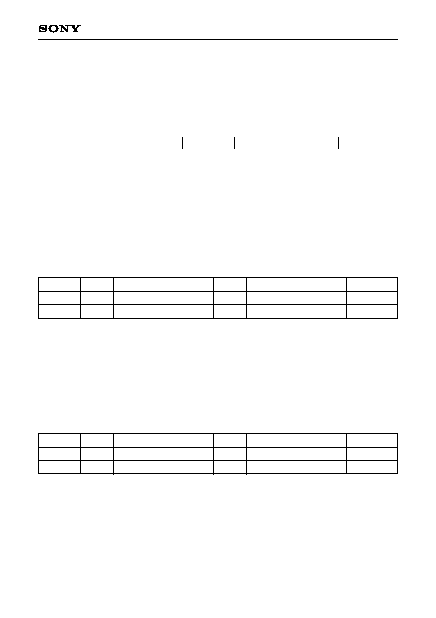
≠ 44 ≠
CXD1818R
bit 2:
PACKMODE (pack mode)
High: The four packs of data starting from the five packs before the subcode sync signal are
written in the buffer as one group of data. In the illustration below, H to K are treated as one
group.
Low: The four packs of data before the subcode sync signal are written in the buffer as one group
of data. In the illustration below, I to L are treated as one group.
SCOR
PACK
from DSP
0
1
2
3
4
5
6
7
8
9
10
11
12
13
14
15
16
17
18
19
H
I
J
K
L
M
N
O
P
Q
R
S
T
PACKMODE
H:
I:
J:
de-interleaved
PACK
Pack using 0 to 7
Pack using 1 to 8
Pack using 2 to 9
1-1-31. 20h, 21h
(1) BFARA#-H, L (buffering area number-high, low) (read/write)
BFARA#-H, L (buffering area number-high, low)
20h (R/W)
21h (R/W)
b7
b6
b5
b4
b3
b2
b1
b8
b0
Adr.
bit7
bit6
bit5
bit4
bit3
bit2
bit1
bit0
Reg.
BFARA#-H
BFARA#-L
The area is read where the data from the CD DSP is buffered.
This register indicates the buffering area when executing a write-only, real-time error correction, or CD-DA
command. Before executing one of these commands, the sub CPU specifies the area where buffering is to
start initially. When the buffering of a sector is completed, this register is incremented.
When executing a subcode buffering command, buffering starts from address 0.
1-1-32. 22h, 23h
(1) CSCTARA-H, L (current sector area-high, low) register (read)
CSCTARA-H, L (current sector area-high, low) register
22h (R)
23h (R)
b7
b6
b5
b4
b3
b2
b1
b8
b0
Adr.
bit7
bit6
bit5
bit4
bit3
bit2
bit1
bit0
Reg.
CSCTARA-H
CSCTARA-L
This register indicates the area number where the current sector is being written.
≠ 45 ≠
CXD1818R
1-1-33. 24h, 25h
(1) DLARA-H, L (drive last area-high, low) register (read/write)
DLARA-H, L (drive last area-high, low) register
24h (R/W)
25h (R/W)
b7
b6
b5
b4
b3
b2
b1
b8
b0
Adr.
bit7
bit6
bit5
bit4
bit3
bit2
bit1
bit0
Reg.
DLARA-H
DLARA-L
This register specifies the last buffering area while the decoder is executing a write-only, real-time error
correction, or CD-DA command. If the ENDLA bit (bit 1) of the DECCTL0 register is set high and the data from
the drive (CD DSP) is written in the area specified by DLARA while the decoder is executing one of the above
commands, subsequent buffering is prohibited.
1-1-34. 27h
(1) TGTMIN (target minute) register (read/write)
TGTMIN (target minute) register
27h (R/W)
b7
b6
b5
b4
b3
b2
b1
b0
Adr.
bit7
bit6
bit5
bit4
bit3
bit2
bit1
bit0
Reg.
TGTMNT
0 to 99 (BCD)
1-1-35. 28h
(1) TGTSEC (target second) register (read/write)
TGTSEC (target second) register
28h (R/W)
b7
b6
b5
b4
b3
b2
b1
b0
Adr.
bit7
bit6
bit5
bit4
bit3
bit2
bit1
bit0
Reg.
TGTSEC
0 to 59 (BCD)
1-1-36. 29h
(1) TGTBLK (target block) register (read/write)
TGTBLK (target block) register
29h (R/W)
b7
b6
b5
b4
b3
b2
b1
b0
Adr.
bit7
bit6
bit5
bit4
bit3
bit2
bit1
bit0
Reg.
TGTBLK
0 to 74 (BCD)
Set the target sector address in these three registers when executing a monitor-only, write-only, or real-time
error correction command. This address is compared with the current sector address, and if they do not match,
TGTNTMT (target not met) status (bit 0 of the DECSTS0 register) is established.
≠ 46 ≠
CXD1818R
1-1-37. 2B to 2Dh
(1) XFRCNT-H, M, L (transfer block counter-high, middle, low) register (read/write)
XFRCNT-H, M, L (transfer block counter-high, middle, low) register
2Bh (R/W)
2Ch (R/W)
2Dh (R/W)
b23
b15
b7
b22
b14
b6
b21
b13
b5
b20
b12
b4
b19
b11
b3
b18
b10
b2
b17
b9
b1
b16
b8
b0
Adr.
bit7
bit6
bit5
bit4
bit3
bit2
bit1
bit0
Reg.
XFRCNT-H
XFRCNT-M
XFRCNT-L
This is a 24-bit register that shows the number of blocks remaining to be transferred. Before the start of the
transfer the sub CPU sets the total number of blocks to be transferred in this register.
This register is decremented as the transfer of each block is completed.
1-1-38. 2Eh, 2Fh
(1) XFRARA-L, H (transfer area-low, high) register (read/write)
XFRARA-L, H (transfer area-low, high) register
2Eh (R/W)
2Fh (R/W)
b7
b6
b5
b4
b3
b2
b1
b8
b0
Adr.
bit7
bit6
bit5
bit4
bit3
bit2
bit1
bit0
Reg.
XFRARA-H
XFRARA-L
During an automatic transfer, this register specifies the initial area from which the transfer is to start. This
register is incremented after a block is transferred. Note that bits 7 to 1 of the XFRCNT-H register should
normally be set low.
1-1-39. 30h
(1) XFRCTL (transfer control) register (write)
30h (W)
"L"
"L"
"L"
"L"
"L"
IGNXF
RSCT
IGNXF
RFST
XSOS
TOP
Adr.
bit7
bit6
bit5
bit4
bit3
bit2
bit1
bit0
Reg.
XFRCTL
bits 7 to 3: RESERVED
Always set low.
bit 2:
IGNXFRSCT (ignore XFRSCT)
High: When both this bit and bit 1 are high, transfer is performed until XFRCNT = 0 (stream
command end) even if the sector information XFRSCT is "0". (This is set when restarting a
transfer which does not need to be stopped.)
Low: The above processing is not performed.
bit 1:
IGNXFRFST (ignore XFRSCT first)
This bit is valid only when XSOSTOP = high.
High: Transfer is performed even when the sector information XFRSCT is "0" only for the initial
sector. (This is set when restarting transfer.)
Low: The above processing is not performed.
bit 0:
XSOSTOP
High: During automatic transfer, when the sector information XFRSCT (transfer sector) is set to "0"
in a transferred sector, transfer is stopped.
Low: Be sure to set the XSOSTOP bit high.
The settings of bits 1 and 2 are cleared for every transfer completion.
Set the XFRCTL register for every transfer command issure.
≠ 47 ≠
CXD1818R
1-1-40. 31h
(1) XFRPOS (first transfer position) register (read/write)
XFRPOS (transfer position) register
31h (R/W)
XFR
POS1
XFR
POS0
Adr.
bit7
bit6
bit5
bit4
bit3
bit2
bit1
bit0
Reg.
XFRPOS
bits 7 to 2: RESERVED
Always set low.
bits 1, 0:
XFRPOS1, 0
These bits specify the initial block position from which transfer is to start when in 512- or 1024-byte
transfer mode (automatic transfer mode). In 1024-byte transfer mode, XFRPOS1 is invalid. This
register is incremented after a block is transferred. This register is invalid in manual transfer mode
and automatic transfer modes other than 512- and 1024-byte mode.
The sub CPU can read the values of XFRARA, XFRPOS, BFBLKC and XFRCNT at any time.
However, because the reads by the sub CPU are not synchronized with the variation of BFBLKC,
note that there is a possibility of an error of ±1 between the value that is read and the actual value.
1-1-41. 33h to 35h
(1) HXFRC-H, M, L (host transfer byte counter-high, middle, low) register (read/write)
HXFRC-H, M, L (host transfer byte counter-high, middle, low) register
33h (R/W)
34h (R/W)
35h (R/W)
b15
b7
b14
b6
b13
b5
b12
b4
b19
b11
b3
b18
b10
b2
b17
b9
b1
b16
b8
b0
Adr.
bit7
bit6
bit5
bit4
bit3
bit2
bit1
bit0
Reg.
HXFRC-H
HXFRC-M
HXFRC-L
In manual transfer mode, these registers set the number of bytes to be transferred. (20 bits) The number of
bytes remaining to be transferred can also be read from this register. Note that bits 7 to 4 of HXFRC-H should
normally be set low.
Note) Send Data (A1h), Send Status (A5h) and Send Message (A7h), which were passed via the buffer,
should not be executed if HADRC-H, M, L are odd addresses and HXFRC-H, M, L are 3 bytes for
setting conditions.
1-1-42. 37h to 39h
(1) HADRC-H, M, L (host address counter-high, middle, low) register (read/write)
HADRC-H, M, L (host address counter-high, middle, low) register
37h (R/W)
38h (R/W)
39h (R/W)
b15
b7
b14
b6
b13
b5
b12
b4
b19
b11
b3
b18
b10
b2
b17
b9
b1
b16
b8
b0
Adr.
bit7
bit6
bit5
bit4
bit3
bit2
bit1
bit0
Reg.
HADRC-H
HADRC-M
HADRC-L
In manual transfer mode, these registers set the head address from which the transfer begins. Note that bits 7
to 4 of HADRC-H should normally be set low.
Note) Send Data (A1h), Send Status (A5h) and Send Message (A7h), which were passed via the buffer,
should not be executed if HADRC-H, M, L are odd addresses and HXFRC-H, M, L are 3 bytes for
setting conditions.

≠ 48 ≠
CXD1818R
1-1-43. 3Bh to 3Dh
(1) SLADR-H, M, L (subcode last address-high, middle, low) register (read/write)
SLADR-H, M, L (subcode last address-high, middle, low) register
3Bh (R/W)
3Ch (R/W)
3Dh (R/W)
b15
b7
b14
b6
b13
b5
b12
b4
b19
b11
b3
b18
b10
b2
b17
b9
b1
b16
b8
b0
Adr.
bit7
bit6
bit5
bit4
bit3
bit2
bit1
bit0
Reg.
SLADR-H
SLADR-M
SLADR-L
These registers specify the last buffering address for subcode buffering commands. If the ENDLA bit (bit 1) of
the DECCTL0 register is set high and the data is written in the buffer address specified by SLADR while the
decoder is executing a subcode buffering command, subsequent buffering is prohibited. Be sure to set these
registers in the order of H
M
L. Note that bits 7 to 4 of SLADR-H should normally be set low.
1-1-44. 3Fh to 41h
(1) CWADRC-H, M, L (CPU write address counter-high, middle, low) register (read/write)
CWADRC-H, M, L (CPU write address counter-high, middle, low) register
3Fh (R/W)
40h (R/W)
41h (R/W)
b15
b7
b14
b6
b13
b5
b12
b4
b19
b11
b3
b18
b10
b2
b17
b9
b1
b16
b8
b0
Adr.
bit7
bit6
bit5
bit4
bit3
bit2
bit1
bit0
Reg.
CWADRC-H
CWADRC-M
CWADRC-L
The sub CPU sets this address when writing Data In the buffer memory. The register is incremented when
data is written in the buffer memory. The sub CPU should set these registers in the order of CWADRC-H, M, L.
Note that bits 7 to 4 of CWADRC-H should normally be set low.
1-1-45. 43h to 45h
(1) CRADRC-H, M, L (CPU read address counter-high, middle, low) register (read/write)
CRADRC-H, M, L (CPU read address counter-high, middle, low) register
43h (R/W)
44h (R/W)
45h (R/W)
b15
b7
b14
b6
b13
b5
b12
b4
b19
b11
b3
b18
b10
b2
b17
b9
b1
b16
b8
b0
Adr.
bit7
bit6
bit5
bit4
bit3
bit2
bit1
bit0
Reg.
CRADRC-H
CRADRC-M
CRADRC-L
The sub CPU sets this address when reading data from the buffer memory. The register is incremented when
data is read from the buffer memory. The sub CPU should set these registers in the order of CRADRC-H, M, L.
Note that bits 7 to 4 of CRADRC-H should normally be set low.
≠ 49 ≠
CXD1818R
1-1-46. 46h, 47h
(1) BFBLKC-H, L (buffer block count-high, low) register (read/write)
BFBLKC-H, L (buffer block count-high, low) register
46h (R/W)
47h (R/W)
b7
b6
b5
b4
b3
b10
b2
b9
b1
b8
b0
Adr.
bit7
bit6
bit5
bit4
bit3
bit2
bit1
bit0
Reg.
BFBLKC-H
BFBLKC-L
This register is a 10-bit counter that indicates the number of blocks in the buffer that can be transferred. Before
activating the decoder, the sub CPU sets the number of blocks that can be transferred.
Once the number of transferable blocks is reached (once the buffer is written with XFRSCT (bit 0) of the
SCTINF register high), the value of BFBLKC is incremented (+1 to 4). The increment value is specified by the
INCBLKS register.
When the transfer of one block is completed, this register is decremented (≠1).
Note that bits 7 to 3 of BFBLKC-H should normally be set low.
1-1-47. 48h, 49h
(1) BFFLRT-H, L (buffer full ratio-high, low) register (read/write)
BFFLRT-H, L (buffer full ratio-high, low) register
48h (R/W)
49h (R/W)
b7
b6
b5
b4
b3
b10
b2
b9
b1
b8
b0
Adr.
bit7
bit6
bit5
bit4
bit3
bit2
bit1
bit0
Reg.
BFFLRT-H
BFFLRT-L
These registers indicate the buffer full ratio.
Note that bits 7 to 3 of BFFLRT-H should normally be set low.
1-1-48. 4Ah, 4Bh
(1) TIMER-H, L (timer-high, low) register (read/write)
TIMER-H, L (timer-high, low) register
4Ah (R/W)
4Bh (R/W)
b15
b7
b14
b6
b13
b5
b12
b4
b11
b3
b10
b2
b9
b1
b8
b0
Adr.
bit7
bit6
bit5
bit4
bit3
bit2
bit1
bit0
Reg.
TIMER-H
TIMER-L
These are the timer settings. The sub CPU should set these registers in the order of TIMER-H, L. After a value
is set in TIMER-L, a timer interrupt occurs when the time specified by (TIMER-H, L)
TIMRRSL passes.
≠ 50 ≠
CXD1818R
1-1-49. 4Ch
(1) TMRRSL (timer resolution) register (read/write)
TMRRSL (timer resolution) register
4Ch (R/W)
b7
b6
b5
b4
b3
b2
b1
b0
Adr.
bit7
bit6
bit5
bit4
bit3
bit2
bit1
bit0
Reg.
TMRRSL
4Dh (R)
Adr.
bit7
bit6
bit5
bit4
bit3
bit2
bit1
bit0
Reg.
ESPSBCAM
This register determines the timer resolution. Assuming the XTL1 clock cycle to be Tw, the timer resolution is
TIMRRSL
◊
16
◊
Tw.
[Example] Setting a resolution of 100µs
(1) XTL1 = 40MHz (Tw = 25ns)
100
◊
1000 / (16
◊
25) = 250 (FAh)
Set FAh in this register. The resolution becomes 100µs.
(2) XTL1 = 33.8688 MHz (Tw = 29.5ns)
100
◊
1000 / (16
◊
29.5) = 211.68
Set D3 or D4h in this register. The resolution becomes 96.7µs or 100.2µs, respectively.
1-1-50. 4Dh
(1) ESPSBCAM (ESP subcode address monitor) register (read)
4Eh (R)
4Fh (R)
b7
b6
b5
b4
b3
b2
b1
b8
b0
Adr.
bit7
bit6
bit5
bit4
bit3
bit2
bit1
bit0
Reg.
STARTARA-H
STARTARA-L
These registers indicate the area from which transfer starts when executing stream processing.
This register indicates the remaining amount of valid subcode data (upper 8 bits) when reading the subcode
while executing an ESP command. The amount of valid subcode data is SBCAM
◊
256 to (SBCAM + 1)
◊
256
bytes.
1-1-51. 4Eh, 4Fh
(1) STARTARA-H, L (start area-high, low) register (read)
STARTARA-H, L (start area-high, low) register
≠ 51 ≠
CXD1818R
1-2. Description of SCSI2 Controller Block Registers
1-2-1. 50h
(1) SCSTS (SCSI module status) register (read)
SCSTS (SCSI module status) register
50h (R)
MON
RST
MON
DBP
TRAG
MODE
0
TBC
ZERO
1
CMDI
NPRG
0
Adr.
bit7
bit6
bit5
bit4
bit3
bit2
bit1
bit0
Reg.
SCSTS
Initial value
This register monitors the various states of the CXD1818R/SCSI2 controller block.
bit 7:
MONRST (monitor RST)
Monitors the SCSI bus XRST signal (positive logic).
bit 6:
MONDBP (monitor DBP)
Monitors the SCSI bus XDBP signal (positive logic).
bit 3:
TARGMODE (target mode indicator)
This bit goes high when the CXD1818R/SCSI2 controller block is in the target status.
bit 2:
TBCZERO (transfer byte counter zero)
This bit goes high while the value of the transfer byte counter (set by the SCSXFRC register) used
to transfer data between the sub CPU and the SCSI is "000".
Note) Even if this value is high, FIFO is not necessarily empty.
bit 0:
CMDINPRG (SCSI module command in progress)
This bit goes high while the CXD1818R/SCSI2 controller block is executing the command written in
the SCCMD register (50h).
(2) SCCMD (SCSI module command) command register (write)
SCCMD (SCSI module command) register
50h (W)
CAT1
CAT0
B05
B04
B03
B02
B01
B00
Adr.
bit7
bit6
bit5
bit4
bit3
bit2
bit1
bit0
Reg.
SCCMD
Commands to the CXD1818R/SCSI2 controller block are written in this register.
bits 7 and 6: CAT1 and 0 (SCSI module command category code 1, 0)
CAT1
0
0
1
1
0
1
0
1
Commands valid in all states
Commands valid in the Disconnect status
Commands valid in the target status
Stream-related commands
CAT0
Mode
bits 5 to 0: B05 to B00 (SCSI module command code B05 to B00)
See the chapter on commands for the details of each command.
≠ 52 ≠
CXD1818R
1-2-2. 51h
(1) Reserved (read/write)
Reserved
51h (R)
51h (W)
Adr.
bit7
bit6
bit5
bit4
bit3
bit2
bit1
bit0
Reg.
Reserved
Initial value
Reserved
Currently not used.
1-2-3. 52h
(1) Reserved (read/write)
Reserved
52h (R)
52h (W)
Adr.
bit7
bit6
bit5
bit4
bit3
bit2
bit1
bit0
Reg.
Reserved
Initial value
Reserved
Currently not used.
1-2-4. 53h
(1) Reserved (read/write)
Reserved
53h (R)
53h (W)
Adr.
bit7
bit6
bit5
bit4
bit3
bit2
bit1
bit0
Reg.
Reserved
Initial value
Reserved
Currently not used.
1-2-5. 54h
(1) SCSCBMON (SCSI control bus monitor) register (read)
SCSCBMON (SCSI control bus monitor) register
54h (R)
MON
BSY
MON
SEL
MON
MSG
MON
CD
MON
IO
MON
REQ
MON
ACK
MON
ATN
Adr.
bit7
bit6
bit5
bit4
bit3
bit2
bit1
bit0
Reg.
SCSCBMON
Initial value
The SCSI control signals on the SCSI bus can be monitored with this register.
All signals are positive logic.
≠ 53 ≠
CXD1818R
bit 7:
MONBSY (monitor BSY)
Monitors the XBSY signal on the SCSI bus.
bit 6:
MONSEL (monitor SEL)
Monitors the XSEL signal on the SCSI bus.
bit 5:
MONMSG (monitor MSG)
Monitors the XMSG signal on the SCSI bus.
bit 4:
MONCD (monitor CD)
Monitors the XCD signal on the SCSI bus.
bit 3:
MONIO (monitor IO)
Monitors the XIO signal on the SCSI bus.
bit 2:
MONREQ (monitor REQ)
Monitors the XREQ signal on the SCSI bus.
bit 1:
MONACK (monitor ACK)
Monitors the XACK signal on the SCSI bus.
bit 0:
MONATN (monitor ATN)
Monitors the XATN signal on the SCSI bus.
(2) Reserved (write)
Reserved
54h (W)
Adr.
bit7
bit6
bit5
bit4
bit3
bit2
bit1
bit0
Reg.
Reserved
Currently not used.
1-2-6. 55h
(1) SCFIFSTS (SCSI FIFO status) register (read)
SCFIFSTS (SCSI FIFO status) register
55h (R)
FIFE
MPTY
1
FIF
FULL
0
FIF
CNT3
0
FIF
CNT2
0
FIF
CNT1
0
FIF
CNT0
0
Adr.
bit7
bit6
bit5
bit4
bit3
bit2
bit1
bit0
Reg.
SCFIFSTS
Initial value
The status of the built-in FIFO can be read from this register.
bit 7:
FIFEMPTY (FIFO empty)
When this bit is high, the FIFO is empty.
bit 4:
FIFFULL (FIFO full)
When this bit is high, the FIFO is full.
bits 3 to 0: FIFCNT3 to 0 (FIFO count 3 to 0)
These bits indicate the used capacity of the built-in FIFO.
(2) Reserved (write)
Reserved
55h (W)
Adr.
bit7
bit6
bit5
bit4
bit3
bit2
bit1
bit0
Reg.
Reserved
Currently not used.
≠ 54 ≠
CXD1818R
1-2-7. 56h
(1) Reserved (read/write)
Reserved
56h (R)
56h (W)
Adr.
bit7
bit6
bit5
bit4
bit3
bit2
bit1
bit0
Reg.
Reserved
Initial value
Reserved
Currently not used.
1-2-8. 57h
(1) SCDATA (SCSI data) register (read/write)
SCDATA (SCSI data) register
57h (R/W)
b07
b06
b05
b04
b03
b02
b01
b00
Adr.
bit7
bit6
bit5
bit4
bit3
bit2
bit1
bit0
Reg.
SCDATA
Initial value
This register is used to transfer data between the sub CPU bus and the SCSI bus.
After the assert SCSI data command has been executed, the value written in this register is output directly to
the SCSI data bus until the deassert SCSI data command is executed. In addition, the SCSI data bus can be
monitored by reading this register.
1-2-9. 58h
(1) SCSXFRC (SCSI sub CPU transfer counter) register (read/write)
58h (R/W)
"L"
"L"
"L"
b4
0
b3
0
b2
0
b1
0
b0
0
Adr.
bit7
bit6
bit5
bit4
bit3
bit2
bit1
bit0
Reg.
SCSXFRC
Initial value
This register sets the number of bytes to be transferred by a phase unit of transfer command from the SCSI to
the sub CPU. The maximum number of bytes which can be sent from the SCSI to the sub CPU with a single
transfer is 16 bytes.

≠ 55 ≠
CXD1818R
1-2-10. 59h
(1) Reserved (read/write)
Reserved
59h (R)
59h (W)
Adr.
bit7
bit6
bit5
bit4
bit3
bit2
bit1
bit0
Reg.
Reserved
Initial value
Reserved
Currently not used.
1-2-11. 5Ah
(1) Reserved (read/write)
Reserved
5Ah (R)
5Ah (W)
Adr.
bit7
bit6
bit5
bit4
bit3
bit2
bit1
bit0
Reg.
Reserved
Initial value
Reserved
Currently not used.
1-2-12. 5Bh
(1) SCSYNCTL (SCSI synchronous transfer control) register (read/write)
SCSYNCTL (SCSI synchronous transfer control) register
5Bh (R/W)
SYXF
RPD3
0
SYXF
RPD2
0
SYXF
RPD1
0
SYXF
RPD0
0
SYXF
ROF3
0
SYXF
ROF2
0
SYXF
ROF1
0
SYXF
ROF0
0
Adr.
bit7
bit6
bit5
bit4
bit3
bit2
bit1
bit0
Reg.
SCSYNCTL
Initial value
This register sets the transfer cycle and transfer offset value during SCSI synchronous transfer. "00h" must be
written in this register when performing asynchronous transfer.
The value written in this register can be read by reading this register.
bits 7 to 4: SYXFRPD3 to 0 (synchronous transfer period 3 to 0)
These bits set the transfer cycle for synchronous transfer. The actual synchronous transfer cycle is
obtained from the formulas below.
When FASTSCSI = 1 (bit 7 of SCCONF1 = 1)
Transfer cycle [ns] =
◊
1000
◊
(4 + SYXFRPDn)
When FASTSCSI = 0 (bit 7 of SCCONF1 = 0)
Transfer cycle [ns] =
◊
1000
◊
(8 + SYXFRPDn)
In addition, the transfer rate at this time is obtained from the formula below.
Transfer rate [MHz] =
◊
1000
f
CLK
[MHz]
1
f
CLK
[MHz]
1
Transfer cycle [ns]
1
≠ 56 ≠
CXD1818R
bits 3 to 0: SYXFROF3 to 0 (synchronous transfer offset 3 to 0)
These bits set the REQ and ACK offset values during synchronous transfer.
When SYXFROF3 to 0 = 0: Asynchronous transfer mode results.
When SYXFROF3 to 0 = 1 to 15: Synchronous transfer is executed at the offset value set in
SYXFROF3 to 0.
1-2-13. 5Ch
(1) Reserved (read/write)
Reserved
5Ch (R)
5Ch (W)
Adr.
bit7
bit6
bit5
bit4
bit3
bit2
bit1
bit0
Reg.
Reserved
Initial value
Reserved
Currently not used.
1-2-14. 5Dh
(1) Reserved (read/write)
Reserved
5Dh (R)
5Dh (W)
Adr.
bit7
bit6
bit5
bit4
bit3
bit2
bit1
bit0
Reg.
Reserved
Initial value
Reserved
Currently not used.
1-2-15. 5Eh
(1) SCSCBCTL (SCSI control bus control) register (read/write)
SCSCBCTL (SCSI control bus control) register
5Eh (R/W)
CTL
BSY
0
CTL
SEL
0
CTL
MSG
0
CTL
CD
0
CTL
IO
0
CTL
REQ
0
Adr.
bit7
bit6
bit5
bit4
bit3
bit2
bit1
bit0
Reg.
SCSCBCTL
Initial value
After the assert SCSI control command has been executed, the SCSI control signals on the SCSI data bus can
be driven directly through this register until the deassert SCSI control command is executed. When each bit is
set high, the corresponding SCSI control signal is also set high. When this register is read, the value written in
this register is read.
Note) Reading this register is not the same as reading the SCSI bus status. The SCSI bus status can be
known by reading the SCSCBMON register (54h).
≠ 57 ≠
CXD1818R
bit 7:
CTLBSY (control BSY)
Controls XBSY signal assert/deassert.
bit 6:
CTLSEL (control SEL)
Controls XSEL signal assert/deassert.
bit 5:
CTLMSG (control MSG)
Controls XMSG signal assert/deassert.
bit 4:
CTLCD (control CD)
Controls XCD signal assert/deassert.
bit 3:
CTLIO (control IO)
Controls XIO signal assert/deassert.
bit 2:
CTLREQ (control REQ)
Controls XREQ signal assert/deassert.
1-2-16. 5Fh
(1) Reserved (read/write)
Reserved
5Fh (R)
5Fh (W)
Adr.
bit7
bit6
bit5
bit4
bit3
bit2
bit1
bit0
Reg.
Reserved
Initial value
Reserved
Currently not used.
1-2-17. 60h
(1) SCCONF0 (SCSI module configuration 0) register (read/write)
SCCONF0 (SCSI module configuration 0) register
60h (R/W)
CDBS
IZDF
0
ANEG
DATA
0
ANEG
RQAK
0
ATNA
RSD
0
ATN
STP
0
ULTRA
SCSI
0
Adr.
bit7
bit6
bit5
bit4
bit3
bit2
bit1
bit0
Reg.
SCCONFIG
Initial value
This register sets the various parameters for the CXD1818R/SCSI2 controller block.
bit 5:
CDBSIZDF (CDB size definition)
Manipulating this bit changes the definition of the SCCDBSIZ register.
When CDBSIZDF is low
69h (R/W)
GP7
B1
0
GP7
B0
0
GP6
B1
0
GP6
B0
0
GP4
B1
0
GP4
B0
0
GP3
B1
0
GP3
B0
0
Adr.
bit7
bit6
bit5
bit4
bit3
bit2
bit1
bit0
Reg.
SCCDBSIZ
Initial value
69h (R/W)
GP7
B1
0
GP7
B0
0
GP6D
B1
0
GP6D
B0
0
GP6C
B1
0
GP6C
B0
0
GP43
B1
0
GP43
B0
0
Adr.
bit7
bit6
bit5
bit4
bit3
bit2
bit1
bit0
Reg.
SCCDBSIZ
Initial value
When CDBSIZDF is high
≠ 58 ≠
CXD1818R
bit 4:
ANEGDATA (active negation on XDB (bits 7 to 0) and XDBP)
If this bit is set high, the XDB (bits 7 to 0) and XDBP pins of the SCSI bus are set to active
negation.
bit 3:
ANEGRQAK (active negation on XREQ and XACK)
If this bit is set high, the XREQ and XACK pins of the SCSI bus are set to active negation.
bit 2:
ATNARSD
High: When the ATN condition is established during the Data In phase (when HSXFRAT = high
(61h bit 5)), transfer is stopped after transfer of the current area has finished.
Low: When the ATN condition is established during the Data In phase (when HSXFRAT = high
(61h bit 5)), transfer is stopped immediately.
bit 1:
ATNSTP
High: When the ATN condition is established during the Message In/Out phase (when HSXFRAT =
low (61h bit 5)), transfer is stopped unconditionally.
Low: Transfer is not stopped even when the ATN condition is established during the Message
In/Out phase (when HSXFRAT = low (61h bit 5)).
bit 0:
ULTRA SCSI
High: ULTRA SCSI mode (independent of FASTSCSI (61h bit 7))
Low: FAST SCSI when FASTSCSI = high (61h bit 7)
SCSI 1 when FASTSCSI = low (61h bit 7)
Ultra SCSI bit
(SCCONF0 bit 0)
"H"
"L"
"L"
Fast SCSI bit
(SCCONF1 bit 7)
◊
"H"
"L"
Mode
Ultra SCSI
Fast SCSI
SCSI 1

≠ 59 ≠
CXD1818R
1-2-18: 61h
(1) SCCONF1 (SCSI module configuration 1) register (read/write)
SCCONF1 (SCSI module configuration 1) register
61h (R/W)
FAST
SCSI
0
HSXF
RSPE
0
HSXF
RAT
0
SPAR
ENB
0
RSLR
TLM3
0
RSLR
TLM2
0
RSLR
TLM1
0
RSLR
TLM0
0
Adr.
bit7
bit6
bit5
bit4
bit3
bit2
bit1
bit0
Reg.
SCMODE
Initial value
This register specifies the SCSI operation mode for the CXD1818R/SCSI2 controller block.
bit 7:
FASTSCSI (Fast SCSI mode)
If this bit is set, synchronous transfer is performed at Fast SCSI timing.
bit 6:
HSXFRSPE (halt SCSI transfer upon SCSI parity error)
This bit determines the operation when a parity error occurs on the SCSI bus during SCSI transfer.
If this bit is set high, transfer is stopped and the command is interrupted. If this bit is set low,
transfer continues. SCSIPERR interrupt is generated in either case.
This bit has no meaning when bit 4 (SPARENB) of the SCCONF1 register is low.
bit 5:
HSXFRAT (halt SCSI transfer upon SCSI attention condition)
This bit determines the operation when the ATN condition is established on the SCSI bus during
SCSI transfer. If this bit is set high, transfer is stopped and the command is interrupted. If this bit is
set low, transfer continues. ATNCOND interrupt is generated in either case.
bit 4:
SPARENB (SCSI parity enable)
If this bit is set high, parity detection is performed on the SCSI bus. While this bit is high, parity
detection is performed during the selection and information transfer phases. If a parity error is
detected while executing selection phase, the CXD1818R/SCSI2 controller block does not respond
to the selection.
bits 3 to 0: RSLRTLM (3 to 0) (Reselection retry limit)
These bits set the number of times for which Reselection is retried until the CXD1818R/SCSI2
controller block informs the sub CPU that Reselection failed when executing Reselection. The
number of retries can be set from 1 to 15 times including the number of Arbitration failures. If "0" is
set, the number of retries is infinite.
1-2-19. 62h
(1) SCCONF2 (SCSI module configuration 2) register (read/write)
SCCONF2 (SCSI module configuration 2) register
62h (R/W)
IDAS
SIGN
0
IDUN
ASGN
0
Adr.
bit7
bit6
bit5
bit4
bit3
bit2
bit1
bit0
Reg.
SCCONF2
Initial value
≠ 60 ≠
CXD1818R
bits 1 to 0: IDASSIGN (ID assigned), IDUNASGN (ID unassigned)
The combination of these two bits is used to set the CXD1818R to the various SCAM states. When
not using SCAM, IDASSIGN must be set to 1 and IDUNASGN to 0.
IDASSIGN
0
0
1
1
0
1
0
1
SCAM monitor status
ID unassigned status
ID assigned status
Undefined
IDUNASGN
Status
SCAM monitor status
In this status, the CXD1818R responds to SCAM selection. If a SCAMSL interrupt is detected in
this status, the CXD1818R must be set to ID unassigned status.
The CXD1818R also responds if selection of the current ID continues for longer than the SCAM
unassigned ID selection response delay (4ms) in this status. If a SLWATN or SLWOATN
interrupt is detected in this status, the CXD1818R must be set to ID assigned status.
ID unassigned status
In this status, the CXD1818R responds only to SCAM selection. If an ID is assigned by SCAM
protocol, the CXD1818R must be set to ID assigned status.
ID assigned status
In this status, the CXD1818R responds only to normal selection, and operates as a SCAM
tolerant device.
1-2-20. 63h
(1) SCRSLTOT (SCSI Reselection time-out) register (read/write)
SCRSLTOT (SCSI Reselection time-out) register
63h (R/W)
RSLT
OUT7
0
RSLT
OUT6
0
RSLT
OUT5
0
RSLT
OUT4
0
RSLT
OUT3
0
RSLT
OUT2
0
RSLT
OUT1
0
RSLT
OUT0
0
Adr.
bit7
bit6
bit5
bit4
bit3
bit2
bit1
bit0
Reg.
SCRSLTOT
Initial value
This register sets the Reselection time-out time. The relationship between the value of this register and the
Reselection time-out is shown below.
Time-out [ms] =
◊
16.384
◊
(RSLTOUTn)
1-2-21. 64h
(1) Reserved (read/write)
Reserved
64h (R)
64h (W)
Adr.
bit7
bit6
bit5
bit4
bit3
bit2
bit1
bit0
Reg.
Reserved
Initial value
Reserved
Currently not used.
f
CLK
[MHz]
1
≠ 61 ≠
CXD1818R
1-2-22. 65h
(1) SCID (SCSI ID) register (read)
SCID (SCSI ID) register
65h (R)
SEL
ID2
0
SEL
ID1
0
SEL
ID0
0
SELI
DINV
0
0
OWN
ID2
0
OWN
ID1
0
OWN
ID0
0
Adr.
bit7
bit6
bit5
bit4
bit3
bit2
bit1
bit0
Reg.
SCID
Initial value
The ID of the initiator which has selected the CXD1818R and other information can be read from this register.
bits 7 to 5: SELID2 to 0 (selected ID)
The ID of the initiator which has selected the CXD1818R can be read from these bits.
Even after Disconnect, this value is held until the CXD1818R responds to the next selection.
bit 4:
SELIDINV (selected ID invalid)
If single initiator mode is used during selection, this bit is set high. This indicates that SELID2 to 0
are invalid at this time.
bits 2 to 0: OWNID2 to 0 (Own ID)
The ID of the CXD1818R/SCSI2 controller block can be read from these bits.
(2) SCID (SCSI ID) register (write)
SCID (SCSI ID) register
65h (W)
REL
ID2
REL
ID1
REL
ID0
OWN
ID2
OWN
ID1
OWN
ID0
Adr.
bit7
bit6
bit5
bit4
bit3
bit2
bit1
bit0
Reg.
SCID
This register sets the initiator ID and the CXD1818R/SCSI2 controller block's own ID when the CXD1818R
performs Reselect.
bits 7 to 5: RSLID2 to 0 (Reselect ID)
These bits set the ID of the initiator to be reselected.
bits 2 to 0: OWNID2 to 0 (Own ID)
These bits set the CXD1818R/SCSI2 controller block's own ID.
Note) Own ID should be set before issuing the enable selection command.
Since the initial value for Own ID is low, if the enable selection command is issued before setting Own
ID, the CXD1818R will respond to the selection for ID = low.
1-2-23. 66h
(1) Reserved (read/write)
Reserved
66h (R)
66h (W)
Adr.
bit7
bit6
bit5
bit4
bit3
bit2
bit1
bit0
Reg.
Reserved
Initial value
Reserved
Currently not used.
≠ 62 ≠
CXD1818R
1-2-24. 67h
(1) Reserved (read/write)
Reserved
67h (R)
67h (W)
Adr.
bit7
bit6
bit5
bit4
bit3
bit2
bit1
bit0
Reg.
Reserved
Initial value
Reserved
Currently not used.
1-2-25. 68h
(1) Reserved (read/write)
Reserved
68h (R)
68h (W)
Adr.
bit7
bit6
bit5
bit4
bit3
bit2
bit1
bit0
Reg.
Reserved
Initial value
Reserved
Currently not used.
1-2-26. 69h
(1) SCCDBSIZ (SCSI CDB size) register (read/write)
SCCDBSIZ (SCSI CDB size) register (when CDBSIZDF = 0)
69h (R/W)
GP7
B1
0
GP7
B0
0
GP6
B1
0
GP6
B0
0
GP4
B1
0
GP4
B0
0
GP3
B1
0
GP3
B0
0
Adr.
bit7
bit6
bit5
bit4
bit3
bit2
bit1
bit0
Reg.
SCCDBSIZ
Initial value
SCCDBSIZ (SCSI CDB size) register (when CDBSIZDF = 1)
69h (R/W)
GP7
B1
0
GP7
B0
0
GP6D
B1
0
GP6D
B0
0
GP6C
B1
0
GP6C
B0
0
GP43
B1
0
GP43
B0
0
Adr.
bit7
bit6
bit5
bit4
bit3
bit2
bit1
bit0
Reg.
SCCDBSIZ
Initial value
When the CXD1818R is selected from the initiator during auto sequence, the number of bytes to be transferred
by command phase is determined by the value of the group code field (bits 7 to 5) in the 1st byte of the SCSI
CDB's operation code. The CXD1818R/SCSI2 controller block determines how many bytes are to be
transferred according to this value, but groups 7, 6, 4 and 3 are reserved or vendor specific for SCSI
standards.
≠ 63 ≠
CXD1818R
The size of the SCSI CDB (command description block) is defined for each value of the group code field (bits 7
to 5) in the 1st byte of the operation code.
Group
Group 0
Group 1
Group 2
Group 3
Group 4
Group 5
Group 6
Group 7
000x xxxx
001x xxxx
010x xxxx
011x xxxx
100x xxxx
101x xxxx
110x xxxx
111x xxxx
6 bytes
10 bytes
10 bytes
Reserved
Reserved
12 bytes
Vendor Specific
Vendor Specific
Operation Code
Byte length
Reserved and vendor specific items in the table above can be defined by this register. The command length
can be set to 6, 10 or 12 bytes.
This register sets the number of bytes to be received when these group commands are received.
When CDBSIZDF is "0", each bit is defined as follows.
bits 7 to 6: GP7B1 to 0 (group 7)
Define the group 7 (vendor specific) command length.
bits 5 to 4: GP6B1 to 0 (group 6)
Define the group 6 (vendor specific) command length.
bits 3 to 2: GP4B1 to 0 (group 4)
Define the group 4 (reserved) command length.
bits 1 to 0: CG3B1 to 0 (group 3)
Define the group 3 (reserved) command length.
When CDBSIZDF is "1", each bit is defined as follows.
bits 7 to 6: GP7B1 to 0 (group 7)
Define the group 7 (reserved) command length.
bits 5 to 4: GP6DB1 to 0 (group 6 Dxh)
Define the group 6D (vendor specific) command length.
This indicates group 6 commands with a CDB operation code of 1101xxxxb.
bits 3 to 2: GP6CB1 to 0 (group 6 Cxh)
Define the group 6C (vendor specific) command length.
This indicates group 6 commands with a CDB operation code of 1100xxxxb.
bits 1 to 0: CG43B1 to 0 (group 4 and group 3)
Define the group 4 (reserved) and group 3 (reserved) command length. The command lengths of
these two groups cannot be defined separately.
Two bits are allotted to each of GP7B (1:0), GP6DB (1:0), GP6CB (bits 1, 0), GP43B (bits 1, 0), GP4B (bits 1,
0) and GP3B (bits 1, 0). Command lengths should be set according to the rules listed in the table below.
GPxxB1
0
0
1
1
0
1
0
1
Undefined
6 bytes
10 bytes
12 bytes
GPxxB0
Number of bytes
≠ 64 ≠
CXD1818R
1-2-27. 6Ah
(1) SCUSTS (SCSI module microcode status) register (read/write)
SCUSTS (SCSI module microcode status) register
6Ah (R)
USTS
B7
0
USTS
B6
0
USTS
B5
0
USTS
B4
0
USTS
B3
0
USTS
B2
0
USTS
B1
0
USTS
B0
0
Adr.
bit7
bit6
bit5
bit4
bit3
bit2
bit1
bit0
Reg.
SCUSTS
Initial value
If this register is read when a sequence command has been completed, it indicates how far the sequence has
progressed.
(2) Reserved (write)
Reserved
6Ah (W)
Adr.
bit7
bit6
bit5
bit4
bit3
bit2
bit1
bit0
Reg.
Reserved
Currently not used.
1-2-28. 6Bh
(1) SCSTCONF (stream configuration) register (read/write)
SCSTCONF (stream configuration) register
6Bh (R)
STDS
CPRV
0
Adr.
bit7
bit6
bit5
bit4
bit3
bit2
bit1
bit0
Reg.
SCSTCONF
Initial value
This register specifies the exception processing method when executing stream commands.
bit 2:
STDSCPRV (stream Disconnect privilege)
If this bit is set high, the bus is disconnected when the buffer becomes empty. If this bit is set low,
the bus is not disconnected.
1-2-29. 6Ch
(1) SCSTRSLM (stream Reselection message) register (read/write)
SCSTRSLM (stream Reselection message) register
6Ch (R/W)
0
0
0
0
0
0
0
0
Adr.
bit7
bit6
bit5
bit4
bit3
bit2
bit1
bit0
Reg.
SCSTRSLM
Initial value
The message to be transferred to the initiator during the Message In phase immediately following Reselection
when executing stream commands is set in this register.
≠ 65 ≠
CXD1818R
1-2-30. 6Dh
(1) SCSTTIOS (stream terminate I/O status) register (read/write)
SCSTTIOS (stream terminate I/O status) register
6Dh (R/W)
0
0
0
0
0
0
0
0
Adr.
bit7
bit6
bit5
bit4
bit3
bit2
bit1
bit0
Reg.
SCSTTIOS
Initial value
The status to be transferred to the initiator after all data has been transferred when executing stream
commands is set in this register.
1-2-31. 6Eh
(1) SCSTTIOM (stream terminate I/O message) register (read/write)
SCSTTIOM (stream terminate I/O message) register
6Eh (R/W)
0
0
0
0
0
0
0
0
Adr.
bit7
bit6
bit5
bit4
bit3
bit2
bit1
bit0
Reg.
SCSTTION
Initial value
The message to be transferred to the initiator after all data has been transferred when executing stream
commands is set in this register.
1-2-32. 6Fh
(1) Reserved (read/write)
Reserved
6Fh (R)
6Fh (W)
Adr.
bit7
bit6
bit5
bit4
bit3
bit2
bit1
bit0
Reg.
Reserved
Initial value
Reserved
Currently not used.

≠ 66 ≠
CXD1818R
1-3. Common Registers
1-3-1. 70h
(1) INTSTS0 (interrupt status 0) register (read)
INTSTS0 (interrupt status 0) register
70h (R)
DEC
INT
0
DEC
TOUT
0
DRV
OVRN
0
CRCT
END
0
CDR
INT
0
ECCO
VRN
0
NOTA
TWSI
0
SHT
SYNC
0
Adr.
bit7
bit6
bit5
bit4
bit3
bit2
bit1
bit0
Reg.
INTSTS0
Initial value
bit 7:
DECINT (decoder interrupt)
This interrupt is generated when the decoder is executing a command.
(1) During execution of a write-only, monitor-only, or real-time error correction command:
If the Header byte is received from the CD DSP when a Sync mark is detected or inserted, the
DECINT status is generated. However, while the Sync mark detection window is open, the
DECINT status is not established if the Sync mark interval is less than 2352 bytes.
(2) During repeat correction execution:
The DECINT status is established each time one correction is completed. (CRCTEND
interrupt?)
(3) During CD-DA command execution:
The DECINT status is established each time 2352 bytes of data are written.
(4) During subcode buffering execution:
The DECINT status is established when the subcode for one sector is written in the buffer.
bit 6:
DECTOUT (decoder time-out)
The DECTOUT status is established when the Sync mark is not detected even after the time it
takes to search 3 sectors (40.6ms at normal-speed playback) has elapsed after the decoder has
been set to the monitor-only, write-only or real-time correction mode.
bit 5:
DRVOVRN (drive overrun)
While the decoder is executing a write-only, real-time correction, or CD-DA command, if buffering
in the area specified by DLARA is completed, the DRVOVRN status results.
bit 4:
CRCTEND (correction end)
If error correction of the CD-ROM data is completed, the CRCTEND status results.
bit 3:
CDRINT (CD-R interrupt)
When the CDRINT status is established, this bit goes high.
bit 2:
ECCOVRN
Generated after error correction of the last (DLARA value) sector is completed.
bit 1:
NOTATWSI
When the status set in the INTCOND0 and INTCOND1 registers occurs in the current sector with
ATWSCTI (DECCTL1 bit 2) high, the NOTATWSI status is established.
bit 0:
SHTSYNC (short sync)
The SHTSYNC status is established when the decoder is operating in the monitor-only, write-only,
real-time correction or asynchronous correction mode.
(2) CLRINT0 (clear interrupt 0) register (write)
CLRINT0 (clear interrupt 0) register
70h (W)
DEC
INT
DEC
TOUT
DRV
OVRN
CRCT
END
CDR
INT
"L"
NOTA
TWSI
SHT
SYNC
Adr.
bit7
bit6
bit5
bit4
bit3
bit2
bit1
bit0
Reg.
CLRINT0
When each bit of this register is set to "1", the corresponding interrupt status of the INTSTS0 register (70h) is
cleared. The bit concerned is automatically set to "0" after its interrupt status has been cleared. Therefore,
there is no need for the sub CPU to reset "0".

≠ 67 ≠
CXD1818R
1-3-2. 71h
(1) INTSTS1 (interrupt status 1) register (read)
INTSTS1 (interrupt status 1) register
71h (R)
ESP
EMP
0
ESP
WINH
0
TIME
R
0
SUBC
SYNC
0
Adr.
bit7
bit6
bit5
bit4
bit3
bit2
bit1
bit0
Reg.
INTSTS1
Initial value
The value of each bit in this register indicates that of the corresponding interrupt status. These bits are not
affected by the values of the INTEN1 register bits.
bit 3:
ESPEMP (ESP empty)
ESPEMP status results when the valid data runs out while executing an ESP command. The
BFEMP bit of the ESPSTS-0 register is also set at this time.
bit 2:
ESPWINH (ESP write inhibit)
ESPWINH status results when any of the BFFUL, ROF or NOGSCR bits of the ESPSTS-0 register
go high while executing an ESP command. In these cases, subsequent buffering is stopped
(ESPWREN = low).
bit 1:
TIMER
TIMER status is established when the time set in the TIMER-H and L registers has elapsed.
bit 0:
SUBCSYNC (subcode sync)
If a subcode Sync mark is detected or inserted while subcode fetching is enabled, the SUBCSYNC
status results.
Note that if the SUBCSYNC interrupt is not cleared within 95 WFCK cycles, the SUBCSYNC status
is not established the next time a subcode Sync mark is detected or inserted. In this event, the
subcode-Q read from the SBQDT register is also not renewed.
(2) CLRINT1 (clear interrupt 1) register (write)
CLRINT1 (clear interrupt 1) register
71h (W)
"L"
"L"
"L"
"L"
ESP
EMP
ESP
WINH
TIME
R
SUBC
SYNC
Adr.
bit7
bit6
bit5
bit4
bit3
bit2
bit1
bit0
Reg.
CLRINT1
When each bit of this register is set to "1", the corresponding interrupt status of the INTSTS1 register (71h) is
cleared. The bit concerned is automatically set to "0" after its interrupt status has been cleared. Therefore,
there is no need for the sub CPU to reset "0".

≠ 68 ≠
CXD1818R
1-3-3. 72h
(1) INTSTS2 (interrupt status 2) register (read)
INTSTS2 (interrupt status 2) register
72h (R)
FUNC
CMPL
0
CMD
IGNR
0
SCSI
RST
0
ATN
COND
0
SCSI
PERR
0
SLW
ATN
0
SLWO
ATN
0
RSL
FAIL
0
Adr.
bit7
bit6
bit5
bit4
bit3
bit2
bit1
bit0
Reg.
INTSTS2
Initial value
When an interrupt is generated, the bit allotted to that interrupt is set to "1".
Each bit is set regardless of the values of the INTEN2 register (76h).
bit 7:
FUNCCMPL (function complete)
Indicates that execution of the command issued to the CXD1818R/SCSI2 controller block has been
completed.
bit 6:
CMDIGNR (command ignored)
Indicates that the command issued to the CXD1818R/SCSI2 controller block was not executed.
This interrupt is generated when the CXD1818R is operating in a mode which does not allow the
command given to the CXD1818R to be executed.
bit 5:
SCSIRST (SCSI reset)
Indicates that the XRST signal was driven on the SCSI bus.
Do not write commands in the SCCMD register (50h) until the sub CPU has confirmed that the
XRST signal is negated on the SCSI bus by reading the MONRST bit (bit 7) of the SCSTS register
(50h).
bit 4:
ATNCOND (ATN condition)
When the CXD1818R/SCSI2 controller block is in the target status, this bit indicates that the
initiator drove XATN.
bit 3:
SCSIPERR (SCSI parity error)
Indicates that a parity error occurred on the SCSI data bus in the SCSI transfer phase or the
selection phase.
This interrupt is not generated when the SPARENB bit of the SCCONF1 register is low.
bit 2:
SLWATN (selection with ATN)
Indicates that the CXD1818R/SCSI2 controller block was selected with ATN by another SCSI
device, and that the CXD1818R/SCSI2 controller block responded to this selection.
bit 1:
SLWOATN (selection without ATN)
Indicates that the CXD1818R/SCSI2 controller block was selected without ATN by another SCSI
device, and that the CXD1818R/SCSI2 controller block responded to this selection.
bit 0:
RSLFAIL (Reselection fail)
Indicates that the CXD1818R/SCSI2 controller block participated in Arbitration during execution of
a Reselect command, and that the CXD1818R/SCSI2 controller block fails or a time-out occurred
during Reselection after acquiring the bus by Arbitration. This interrupt is generated only when
Reselection fail is repeated for the number of times specified by the RSLRTLM (3:0) bit of the
SCCONF1 register.
(2) CLRINT2 (clear interrupt 2) register (write)
CLRINT2 (clear interrupt 2) register
72h (W)
FUNC
CMPL
CMD
IGNR
SCSI
RST
ATN
CONT
SCSI
PERR
SLW
ATN
SLWO
ATN
RSL
FAIL
Adr.
bit7
bit6
bit5
bit4
bit3
bit2
bit1
bit0
Reg.
CLRINT2
When each bit of this register is set to "1", the corresponding interrupt status of the INTSTS2 register (72h) is
cleared. The bit concerned is automatically set to "0" after its interrupt status has been cleared. Therefore,
there is no need for the sub CPU to reset "0".
≠ 69 ≠
CXD1818R
1-3-4. 73h
(1) INTSTS3 (interrupt status 3) register (read)
INTSTS3 (interrupt status 3) register
73h (R)
SCAM
INIF
0
SCAM
SL
0
Adr.
bit7
bit6
bit5
bit4
bit3
bit2
bit1
bit0
Reg.
INTSTS3
Initial value
When an interrupt is generated, the bit allotted to that interrupt is set to "1".
Each bit is set regardless of the values of the INTEN3 register (77h).
bit 1:
SCAMINF (SCAM initiation fail)
Indicates that the CXD1818R/SCSI2 controller block participated in SCAM initiation and failed at
Arbitration.
bit 0:
SCAMSL (SCAM selection)
Indicates that the CXD1818R/SCSI2 controller block was selected with SCAM selection by another
SCSI device, and that the CXD1818R/SCSI2 controller block responded to this selection.
(2) CLRINT3 (clear interrupt 3) register (write)
CLRINT3 (clear interrupt 3) register
73h (W)
SCAM
INIF
SCAM
SL
Adr.
bit7
bit6
bit5
bit4
bit3
bit2
bit1
bit0
Reg.
CLRINT2
When each bit of this register is set to "1", the corresponding interrupt status of the INTSTS3 register (73h) is
cleared. The bit concerned is automatically set to "0" after its interrupt status has been cleared. Therefore,
there is no need for the sub CPU to reset "0".

≠ 70 ≠
CXD1818R
1-3-5. 74h
(1) INTEN0 (interrupt enable 0) register (read/write)
INTEN0 (interrupt enable 0) register
74h (R/W)
DEC
INT
0
DEC
TOUT
0
DRV
OVRN
0
CRCT
END
0
CDR
INT
0
NOTA
TWSI
0
SHT
SYNC
0
Adr.
bit7
bit6
bit5
bit4
bit3
bit2
bit1
bit0
Reg.
INTEN0
Initial value
Setting each bit of this register high enables interrupt requests to the sub CPU from this IC in response to the
corresponding interrupt status. (In other words, if that interrupt status results, the INT pin goes active.) The
value of each bit in this register has no effect on their corresponding interrupt status.
bit 7:
DECINT (decoder interrupt)
bit 6:
DECTOUT (decoder time-out)
bit 5:
DRVOVRN (drive overrun)
bit 4:
CRCTEND (correction end)
bit 3:
CDRINT (CD-R interrupt)
bit 1:
NOTATWSI
bit 0:
SHTSYNC (short sync)
1-3-6. 75h
(1) INTEN1 (interrupt enable 1) register (read/write)
INTEN1 (interrupt enable 1) register
75h (R/W)
ESP
EMP
0
ESP
WINH
0
TIME
R
0
SUBC
SYNC
0
Adr.
bit7
bit6
bit5
bit4
bit3
bit2
bit1
bit0
Reg.
INTEN1
Initial value
Setting each bit of this register high enables interrupt requests to the sub CPU from this IC in response to the
corresponding interrupt status. (In other words, if that interrupt status results, the INT pin goes active.) The
value of each bit in this register has no effect on their corresponding interrupt status.
bit 3:
ESPEMP (ESP empty)
bit 2:
ESPWINH (ESP write inhibit)
bit 1:
TIMER
bit 0:
SUBCSYNC (subcode sync)

≠ 71 ≠
CXD1818R
1-3-7. 76h
(1) INTEN2 (interrupt enable 2) register (read/write)
INTEN2 (interrupt enable 2) register
76h (R/W)
FUNC
CMPL
0
CMD
IGNR
0
SCSI
RST
0
ATN
COND
0
SCSI
PERR
0
SLW
ATN
0
SLWO
ATN
0
RSL
FAIL
0
Adr.
bit7
bit6
bit5
bit4
bit3
bit2
bit1
bit0
Reg.
INTEN2
Initial value
Setting each bit of this register high enables interrupt requests to the sub CPU from this IC in response to the
corresponding interrupt status. (In other words, if that interrupt status results, the INT pin goes active.) The
value of each bit in this register has no effect on their corresponding interrupt status.
bit 7:
FUNCCMPL (function complete)
bit 6:
CMDIGNR (command ignored)
bit 5:
SCSIRST (SCSI reset)
bit 4:
ATNCOND (ATN condition)
bit 3:
SCSIPERR (SCSI parity error)
bit 2:
SLWATN (selection with ATN)
bit 1:
SLWOATN (selection without ATN)
bit 0:
RSLFAIL (Reselection fail)
1-3-8. 77h
(1) INTEN3 (interrupt enable 3) register (read/write)
INTEN3 (interrupt enable 3) register
77h (R/W)
SCAM
INIF
0
SCAM
SL
0
Adr.
bit7
bit6
bit5
bit4
bit3
bit2
bit1
bit0
Reg.
INTEN3
Initial value
Setting each bit of this register high enables interrupt requests to the sub CPU from this IC in response to the
corresponding interrupt status. (In other words, if that interrupt status results, the INT pin goes active.) The
value of each bit in this register has no effect on their corresponding interrupt status.
bit 1:
SCAMINIF (SCAM initiation fail)
bit 0:
SCAMSL (SCAM selection)
≠ 72 ≠
CXD1818R
1-3-9. 78h
(1) INTSRC (interrupt source) register (read)
INTSRC (interrupt source) register
78h (R)
SCSI
REL
0
SCTM
REL
0
DEC
REL
0
Adr.
bit7
bit6
bit5
bit4
bit3
bit2
bit1
bit0
Reg.
INTSRC
Initial value
The internal block interrupt which drove the interrupt pin can be known by reading this register.
bits 7 to 3: RESERVED
bit 2:
SCSIREL (SCSI related)
When this bit is high, this indicates that the interrupt pin is being driven by an INTSTS2 or INTSTS3
register interrupt which is enabled by the INTEN2 or INTEN3 register.
bit 1:
SCTMREL (subcode and timer related)
When this bit is high, this indicates that the interrupt pin is being driven by an INTSTS1 register
interrupt which is enabled by the INTEN1 register.
bit 0:
DECREL (decoder related)
When this bit is high, this indicates that the interrupt pin is being driven by an INTSTS0 register
interrupt which is enabled by the INTEN0 register.
(2) Reserved (write)
Reserved
78h (W)
Adr.
bit7
bit6
bit5
bit4
bit3
bit2
bit1
bit0
Reg.
Reserved
Currently not used.
1-3-10. 79h
(1) ESPARA (ESP area) register (read/write)
ESPARA (ESP area) register
79h (R)
79h (W)
"L"
Adr.
bit7
bit6
bit5
bit4
bit3
bit2
bit1
bit0
Reg.
ESPARA
ESPARA
bits 6 to 0: Frame count setting = 53 to 6F (83 to 111)
These bits set the boundary between the CDDA data buffer and the subcode P-W buffer.
79h write
bit 7:
RESERVED
Always set low.
79h read
bit 7:
Not used (low).
≠ 73 ≠
CXD1818R
1-3-12. 7Ch
(1) ESPCTL0 (ESP control 0) register (write)
ESPCTL0 (ESP control 0) register
1-3-11. 7Ah, 7Bh
(1) SUBBLCK-H register (read/write)
SUBBLCK-H register
7Ah (R/W)
7Bh (R/W)
b7
b6
b5
b4
b3
b10
b2
b9
b1
b8
b0
Adr.
bit7
bit6
bit5
bit4
bit3
bit2
bit1
bit0
Reg.
SUBBLCK-H
SUBBLCK-L
When a value is set in this register, this setting value is subtracted from the BFBLKC value.
SUBBLCK-H bits 7 to 3: RESERVED
Always set low.
bit 7:
ESPARST (ESP area reset)
Set this bit high to reset only the subcode buffering address during the execution of an ESP
command.
bit 6:
RESERVED
Always set low.
bit 5:
BCKFED
High: When the rising edge of LRCK and the rising edge of BCLK match.
Low: When the rising edge of LRCK and the falling edge of BCLK match.
bit 4:
SQOK (subcode-Q OK)
When the subcode-Q is continuous, this bit goes high. When BFFUL = low, ROF = low and GSCR
is detected, the valid address is updated at the timing of the next SBCSYNC. Be sure to check the
QVLD status of the ESPSTS1 register at the next SBCSYNC when this bit is set high.
bit 3:
ESPWREN (ESP write enable)
CD-DA data buffering starts when this bit is set high.
bit 2:
ESPRDEN (ESP read enable)
Audio data playback starts when this bit is set high.
bit 1:
ESPRST (ESP reset)
Set this bit high to reset the ESP block.
Buffering address reset and read/write to the buffer are stopped.
bit 0:
GRST
Set this bit high when unlocking GRSCOR.
7Ch (W)
ESPA
RST
"L"
BCK
FED
SQOK
ESPW
REN
ESPR
DEN
ESP
RST
GRST
Adr.
bit7
bit6
bit5
bit4
bit3
bit2
bit1
bit0
Reg.
ESPCTL0

≠ 74 ≠
CXD1818R
(2) ESPSTS0 (ESP status 0) register (read)
ESPSTS0 (ESP status 0) register
bit 7:
ROF (DSP RAM overflow)
When the CD DSP RAM overflows (XROF = low), this bit goes high. In this case, subsequent
buffering is stopped (ESPWREN = low).
bit 6:
BMFUL: (buffer memory full)
When there is no space to write CD-DA data in the buffer memory, this bit goes high. In this case,
subsequent buffering is stopped (ESPWREN = low).
bit 5:
BFEMP (buffer memory empty)
When the buffer memory runs out of valid data, this bit goes high. In this case, audio playback is
stopped (ESPRDEN = low) and DACD output goes low.
bit 4:
NOGSCR (no GSCR)
When the GSCR signal was not detected in the frame where buffering starts, this bit goes high. In
this case, buffering is stopped (ESPWREN = low).
bit 3:
ESPWREN (ESP write enable)
Indicates that CD-DA data is being buffered.
bit 2:
ESPRDEN (ESP read enable)
Indicates that audio data is being played back. ESP read enable (performance start) when high.
bit 1:
Not used (high).
bit 0:
Not used (high).
7Ch (R)
ROF
BMFUL
BFEMP NOGSCR
ESPW
REN
ESPR
DEN
Adr.
bit7
bit6
bit5
bit4
bit3
bit2
bit1
bit0
Reg.
ESPSTS0
≠ 75 ≠
CXD1818R
1-3-13. 7Dh
(1) ESPCTL1 (ESP control 1) register (write)
ESPCTL1 (ESP control 1) register
bit 7:
LSB1ST
High: DACD output is LSB first.
Low: DACD output is MSB first.
bits 6 to 0: RESERVED
Always set low.
7Dh (W)
LSB1ST
"L"
"L"
"L"
"L"
"L"
"L"
"L"
Adr.
bit7
bit6
bit5
bit4
bit3
bit2
bit1
bit0
Reg.
ESPCTL1
(2) ESPSTS1 (ESP status 1) register (read)
ESPSTS1 (ESP status 1) register
This register indicates the status while executing an ESP command. Bits 1 and 0 are valid from SBCSYNC to
the next SBCSYNC.
bit 7:
Not used (low).
bits 6 to 2: AM17 to 13
These bits indicate the remaining amount of valid data (upper 5 bits). The valid data is AM
◊
8K to
(AM + 1)
◊
8K bytes.
bit 1:
GROK (GSCR OK)
Indicates that GSCR was detected.
bit 0:
QVLD: (Sub Q valid)
Indicates that the valid address was updated.
7Dh (R)
GROK
QVLD
Adr.
bit7
bit6
bit5
bit4
bit3
bit2
bit1
bit0
Reg.
ESPSTS1

≠ 76 ≠
CXD1818R
1-3-14. 7Eh
(1) INTCOND0 register (read/write)
INTCOND0 register
7Eh (R/W)
BFSH
DRFLG
0
EDC
ALLO
0
COR
INH
0
ERIN
BLK
0
COR
DONE
0
EDC
NG
0
ECC
NG
0
TGTN
TMET
0
Adr.
bit7
bit6
bit5
bit4
bit3
bit2
bit1
bit0
Reg.
INTCOND0
Initial value
Setting each bit of this register high establishes the NOTATWSI status when the status corresponding to
CSCTARA is high.
bit 7:
BFSHDRFLG
bit 6:
EDCALLO
bit 5:
CORINH
bit 4:
ERINBLK
bit 3:
CORDONE
bit 2:
EDCNG
bit 1:
ECCNG
bit 0:
TGTNTMET
1-3-15. 7Fh
(1) INTCOND1 register (read/write)
INTCOND1 register
7Fh (R/W)
C
MODE
0
C
FORM
0
Adr.
bit7
bit6
bit5
bit4
bit3
bit2
bit1
bit0
Reg.
INTCOND1
Initial value
bit 2:
CMFCMPEN (CMODE, CFORM compare enable)
Setting this bit high establishes the NOTATWSI status when CMODE and CFROM (DECSTS1 bits
1 and 0) of CSCTARA does not match this register bits 1 and 0.
bit 1:
CMODE
bit 0:
CFORM
≠ 77 ≠
CXD1818R
[2] Description of SCSI Controller Block Commands
The CXD1818R/SCSI2 core is designed to automatically execute procedures other than data transfer to the
greatest extent possible in order to reduce data transfer overloads.
CXD1818R/SCSI2 core command set
CAT0 CMD5 CMD4 CMD3 CMD2 CMD1 CMD0
Description
CAT1
0
0
0
0
0
0
0
0
0
CAT1
0
0
0
0
CAT1
1
1
1
1
1
1
1
1
1
1
1
1
1
CAT1
1
1
1
1
1
0
0
0
0
0
0
0
0
0
CAT0
1
1
1
1
CAT0
0
0
0
0
0
0
0
0
0
0
0
0
0
CAT0
1
1
1
1
1
0
0
0
0
0
0
0
0
0
CMD5
0
0
0
0
BUF
0
0
0
0
0
CMD5
0
0
0
0
0
0
0
0
0
0
0
0
0
0
CMD4
0
0
0
0
SUB
0
0
0
0
0
CMD4
0
0
0
0
0
0
0
0
0
0
0
0
1
1
CMD3
0
0
0
0
CMD3
0
0
0
0
0
0
0
0
1
1
1
1
1
CMD3
0
0
0
0
0
0
0
0
1
1
1
1
0
0
CMD2
0
0
0
0
CMD2
0
0
0
0
1
1
1
1
0
0
0
0
1
CMD2
0
0
0
0
1
0
0
1
0
0
1
1
0
0
CMD1
0
0
1
1
CMD1
0
0
1
1
0
0
1
1
0
0
1
1
0
CMD1
0
0
1
1
0
0
1
1
0
1
0
1
0
1
CMD0
0
1
0
1
CMD0
0
1
0
1
0
1
0
1
0
1
0
1
0
CMD0
0
1
0
1
0
NOP
CHIP Reset
Flush FIFO
Assert SCSI Control
Deasert SCSI Control
Assert SCSI Data
Deasert SCSI Data
Enable Selection
Disable Selection
Description
Reselect and Send Message (s)
Initiate SCAM
Reselect, Send Message (s) and Receive Data
Reselect, Send Message (s) and Send Data
Description
Receive Data
Send Data
Reserved
Reserved
Reseive Command
Send Status
Receive Message
Send Message
Disconnect
Send Message (s) and Disconnect
Terminate I/O and bus free
Terminate I/O and link
Receive Command Sequence
Description
Stream Abort
Stream and Stop
Stream and Bus Free
Stream and Link
Stream Pause
Either "1" or "0" can be written. However, if the BUF bit is "1", "0" must be written for the SUB bit.
States which allow commands to be executed are limited for each category.
CAT1
0
0
1
1
0
1
0
1
Can be executed in all states
Can be executed only in the Disconnect status
Can be executed only in the target mode
Stream commands
CAT0
Description

≠ 78 ≠
CXD1818R
2-1. Precautions when Executing Commands
In the CXD1818R, an interrupt is generated for the sub CPU at the point when an interrupt event occurs.
However, the sub CPU must wait until a FUNCCMPL interrupt (INTSTS2, bit 7) is generated.
2-2. Category 00 Commands
These commands can be executed regardless of the CXD1818R/SCSI2 core status.
2-2-1. NOP (00h)
Description: When this command is issued, a FUNCCMPL interrupt is generated but no other action is taken.
Preparation: None
Operation:
After this command is issued, the CMDINPRG bit (SCSTS register (50h), bit 0) goes high. Then,
after the FUNCCMPL interrupt is generated, the CMDINPRG bit goes low and the command is
completed.
Interrupt:
FUNCCMPL function complete (INTSTS2 register (72h), bit 7)
Microcode status:
The microcode status has no meaning with this command.
2-2-2. CHIP reset (01h)
Description: This command initializes the registers (50h to 6Fh, 72h to 73h, and 76h to 77h) inside the SCSI
block and resets the microcode PC.
In this event, commands currently being executed are forcibly interrupted.
Preparation: None
Operation:
Commands are normally decoded by a microprogram in the CXD1818R/SCSI2 core. However,
when this command is issued, the CXD1818R/SCSI2 core decodes this command with the
hardware instead of the microcode and generates a reset signal internally. Commands currently
being executed are also forcibly interrupted.
Interrupt:
An interrupt is not generated. After this command is issued, the sub CPU must wait for 150ns
before issuing the next command.
Microcode status:
The microcode status has no meaning with this command.
2-2-3. Flush FIFO (03h)
Description: This command clears the FIFO address counter, invalidates all data within the FIFO, and sets the
FIFO to empty status.
Preparation: None
Operation:
After this command is issued, the FIFO is set to empty status.
Interrupt:
An interrupt is not generated.
If the XWAT pin is not used, wait 150ns or more after this command is issued before issuing the
next command.
Microcode status:
The microcode status has no meaning with this command.

≠ 79 ≠
CXD1818R
2-2-4. Assert SCSI control (04h)
Description: This command enables direct control of the SCSI control bus signals through the SCSCBCTL
register (5Eh).
Preparation: When this command is issued, the value of the SCSCBCTL register is output as is to the SCSI
bus. Therefore, be sure to check the contents of the SCSCBCTL register before executing this
command.
Operation:
This command enables direct control of the SCSI control bus signals and is then completed.
After this command is executed, if each bit of the SCSCBCTL register (5Eh) allotted to each SCSI
control bus signal is set high, the corresponding signal is driven.
Interrupt:
An interrupt is not generated.
If the XWAT pin is not used, wait 150ns or more after this command is issued before issuing the
next command.
Microcode status:
The microcode status has no meaning with this command.
2-2-5. Deassert SCSI control (05h)
Description: This command prohibits direct control of the SCSI control bus signals through the SCSCBCTL
register (5Eh).
Preparation: None
Operation:
This command prohibits direct control of the SCSI control bus signals and is then completed.
The SCSI control signals which were controlled directly from the SCSCBCTL register (5Eh) are
deasserted. The data written in the SCSCBCTL register is held.
Interrupt:
An interrupt is not generated.
If the XWAT pin is not used, wait 150ns or more after this command is issued before issuing the
next command.
Microcode status:
The microcode status has no meaning with this command.
2-2-6. Assert SCSI data (06h)
Description: This command enables direct control of the SCSI data bus through the SCDATA register (57h).
Control is disabled immediately after resetting the hardware or issuing the chip reset command.
Preparation: None
Operation:
Direct control of each bit of the SCSI data bus is enabled and then the command is completed.
After this command is executed, if data is written in the SCDATA register (57h), this data is output
directly to the SCSI data bus. At this time, the FIFO does not perform FIFO functions.
Interrupt:
An interrupt is not generated.
If the XWAT pin is not used, wait 150ns or more after this command is issued before issuing the
next command.
Microcode status:
The microcode status has no meaning with this command.

≠ 80 ≠
CXD1818R
2-2-7. Deassert SCSI data (07h)
Description: This command prohibits direct control of the SCSI data bus through the SCDATA register (57h).
Direct control of the SCSI data bus is disabled immediately after resetting the hardware or issuing
the chip reset command.
Preparation: None
Operation:
When this command is executed, direct control of the SCSI data bus is prohibited and then the
command is completed. The FIFO operates normally after the command is executed.
Interrupt:
An interrupt is not generated.
If the XWAT pin is not used, wait 150ns or more after this command is issued before issuing the
next command.
Microcode status:
The microcode status has no meaning with this command.
2-2-8. Enable selection (08h)
Description: This command allows the CXD1818R/SCSI2 core to respond to the selection. The
CXD1818R/SCSI2 core does not respond to the selection in the following cases.
a) After chip reset
b) After issuing the chip reset command
c) After the Bus-Free status is established by a Disconnect command
d) After the Bus-Free status is established by a terminate (including stream and Bus-Free)
command
Operation following the execution of this command varies according to the settings of the
IDASSIGN and IDUNASGN bits of the SCCONF2 register (62h).
a) IDASSIGN = 0, IDUNASGN = 0: SCAM monitor status
1) The CXD1818R/SCSI2 core responds to SCAM selection.
2) The CXD1818R/SCSI2 core responds when selection of the current ID continues for longer
than the SCAM unassigned ID selection response delay (4ms).
b) IDASSIGN = 0, IDUNASGN = 1: ID unassigned status
1) The CXD1818R/SCSI2 core responds to SCAM selection.
c) IDASSIGN = 1, IDUNASGN = 0: ID assigned status
1) The CXD1818R/SCSI2 core responds to normal selection.
Responding to SCAM selection
If SCAM selection is detected in the SCAM monitor or ID unassigned status, a SCAMSL
interrupt and then a FUNCCMPL interrupt are generated. After this, the sub CPU must execute
SCAM protocol using assert SCSI control and assert SCSI data.
Responding to selection
When normal selection is detected during the ID assigned status, or when selection of the
current ID continues for longer than 4 ms in the SCAM monitor status, the following sequences
are executed.
a) When responding to selection with ATN
Bus-Free
Arbitration
Selection with ATN
Message Out
Command
b) When responding to selection without ATN
Bus-Free
Arbitration
Selection without ATN
Command
≠ 81 ≠
CXD1818R
Preparation: The following settings must be made before executing the enable selection command.
1) Set the SCCONF0 register (60h)
Set the appropriate values.
2) Set the SCID register (65h)
Set the characteristic SCSI ID of the CXD1818R/SCSI2 core. The initial SCSI ID setting is "0".
Therefore, be sure to set the SCSI ID before executing the enable selection command.
3) Set the SCCONF1 register (61h).
Set the number of Reselection retries for the CXD1818R/SCSI2 core.
4) Set the SCCONF2 register (62h)
Set the CXD1818R status after executing the enable selection command.
Operation:
Enable selection operation
If this command is issued, the CXD1818R/SCSI2 core is set to status which enables selection and
then a FUNCCMPL interrupt is generated.
Interrupt:
An interrupt is not generated.
If the XWAT pin is not used, wait 150ns or more after this command is issued before issuing the
next command.
Microcode status:
The microcode status has no meaning with this command.
(1) When responding to selection with ATN
Bus-Free
Arbitration
Selection with ATN
Message Out
Command
Operation:
1) When the characteristic SCSI ID of the CXD1818R/SCSI2 core is detected by selection, the
CXD1818R/SCSI2 core responds to this and generates a SLWATN interrupt.
2) Operation shifts to the Message Out phase and a message is received from the initiator.
3) Operation shifts to the command phase and the CDB (command description block) is received.
The number of bytes received is determined inside the CXD1818R/SCSI2 core from the group
code field (bits 7 to 5) in the 1st CDB byte of the operation code. Groups for which the CDB
size is undefined by SCSI standards (groups 7, 6, 4 and 3) can be defined by the SCCDBSIZ
register (69h).
Interrupt:
SLWATN
Selection with ATN (INTSTS2 register (72h), bit 2)
FUNCCMPL
Function complete (INTSTS2 register (72h), bit 7)
Microcode status:
The microcode status value when the command is completed has the following meanings.
Code
01h
02h
An error occurred in the Message Out phase.
A valid identify message was received in the Message Out phase and operation shifted
to the command phase.
Description

≠ 82 ≠
CXD1818R
(2) When responding to selection without ATN
Bus-Free
Arbitration
Selection without ATN
Command
Operation:
1) When the characteristic SCSI ID of the CXD1818R/SCSI2 core is detected by selection, the
CXD1818R/SCSI2 core responds to this and generates a SLWOATN interrupt.
2) Operation shifts to the command phase and the CDB (command description block) is received.
The number of bytes received is determined inside the CXD1818R/SCSI2 core from the group
code field (bits 7 to 5) in the 1st CDB byte of the operation code. Groups for which the CDB
size is undefined by SCSI standards (groups 7, 6, 4 and 3) can be defined by the SCCDBSIZ
register (69h).
Interrupt:
SLWOATN
Selection without ATN (INTSTS2 register (72h), bit 1)
FUNCCMPL
Function complete (INTSTS2 register (72h), bit 7)
Microcode status:
The microcode status value when the command is completed has the following meaning.
Code
02h
Operation shifted to the command phase.
Description
(3) When responding to SCAM selection
Bus-Free
Arbitration
SCAM selection
Operation:
1) If SCAM selection is detected, a SCAMSL interrupt and then a FUNCCMPL interrupt are
generated, and the command is completed.
2) Following this, the sub CPU must execute SCAM protocol using assert SCSI control and assert
SCSI data.
Interrupt:
SCAMSL
SCAM Selection (INTSTS3 register (73h), bit 0)
FUNCCMPL
Function complete (INTSTS2 register (72h), bit 7)
Microcode status:
In this case, the microcode status value has no meaning.
2-2-9. Disable selection (09h)
Description: This command sets the CXD1818R/SCSI2 core so that it does not respond to selection from
another SCSI device.
Operation:
If this command is issued, the CXD1818R/SCSI2 core is set so that it does not respond to
selection from another SCSI device and then the command is completed.
Interrupt:
An interrupt is not generated.
If the XWAT pin is not used, wait 150 ns or more after this command is issued before issuing the
next command.
Microcode status:
In this case, the microcode status value has no meaning.

≠ 83 ≠
CXD1818R
2-3. Category 01 Commands
These commands can be executed only in the Disconnect status.
2-3-1. Reselect sequences (40h, 42h, 43h)
Description: These are auto sequence commands which are executed when attempting reconnection with the
initiator after Disconnect.
The Reselect command has the following two levels.
a) After Reselect, operation shifts to the Message In phase and the message is transferred.
1) Reselect and Send Message(s) (40h)
Bus-Free
Arbitration
Reselection
Message In
b) Data transfer (Data In or Data Out phase) is executed after a).
1) Reselect, Send Message(s) and Receive Data (42h)
Bus-Free
Arbitration
Reselection
Message In
Data Out
2) Reselect, Send Message(s) and Send Data (43h)
Bus-Free
Arbitration
Reselection
Message In
Data In
Preparation: A number of operations must be performed before issuing this command.
Common operations:
1) Specify the CXD1818R operation with the SCCONF0 (60h), SCCONF1 (61h) and SCCONF2
(62h) registers.
2) Set the SCSI ID of the initiator to be reselected and the CXD1818R's own SCSI ID in the
SCID register (65h).
3) Set the FIFO to empty status with the Flush FIFO command and then write the message to
be transferred in the Message In phase in the FIFO.
Only when transferring data after executing the Message In phase:
4) The decoder block side must be prepared for transfer in advance using Reselect, Send
Message(s) and Receive/Send Data.
Operation:
Bus-Free
Arbitration
Reselection
If the Reselect command is executed, first the CXD1818R/SCSI2 core first waits for Bus-Free and
then enter Arbitration. Upon successfully winning the Arbitration, it then shifts to Reselection.
a) When the RSLRTLM (3 to 0) bit of the SCCONF1 register is "00h":
This sequence is repeated until both Arbitration and Reselection are completed successfully.
b) When the RSLRTLM (3 to 0) bit of the SCCONF1 register is greater than "00h":
This sequence is repeated for the number of times set by RSLRTLM. When the number of
times reaches the set number, processing stops, a RSLFAIL interrupt and then a FUNCCMPL
interrupt are generated, and then the command is completed.
When the CXD1818R acquires the right to use the bus during the Arbitration phase, operation
proceeds to the next step only if reconnection with the initiator is successful in the Reselection
phase.
Message In phase
If reconnection is successful, operation shifts to the Message In phase and the message
prepared beforehand in the FIFO, before issuing the command, is transferred to the initiator. If
the attention condition is established during the transfer, ATNCOND and FUNCCMPL interrupts
are generated and transfer stops at that point. However, the first byte of the message (normally
identify) is always transferred.
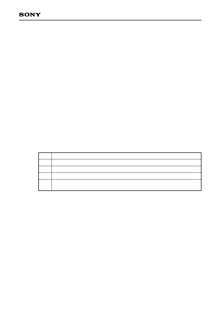
≠ 84 ≠
CXD1818R
Data In/Data Out phase
Operation shifts to either the Data In or Data Out phase as specified by the command only
when the attention condition was not generated by Reselect, Send Message (s) and
Receive/Send Data during the Message In phase. Transfer is performed in the DMA mode
between the buffer and the SCSI. If the attention condition is established or a parity error
occurs on the SCSI bus during the transfer, the corresponding interrupts are generated.
Whether or not transfer is stopped by these factors is determined by the setting of the
HSXFRSPE or HSXFRAT bits of the SCCONF1 register.
Interrupt:
If the transfer is completed normally without problems:
FUNCCMPL Function complete (INTSTS2 register (72h), bit 7)
If the CXD1818R/SCSI2 core is selected immediately after the command is issued or it fails at
Arbitration:
SLWOATN
Selected without ATN (INTSTS2 register (72h), bit 1)
SLWATN
Selected with ATN (INTSTS2 register (72h), bit 2)
FUNCCMPL Function complete (INTSTS2 register (72h), bit 7)
If the CXD1818R/SCSI2 core fails at Arbitration or Reselection:
RSLFAIL
Reselection fail (INTSTS2 register (72h), bit 0)
FUNCCMPL Function complete (INTSTS2 register (72h), bit 7)
Microcode status:
The microcode status value when the command is completed has the following meanings.
Code
00h
01h
02h
03h
Completed normally.
Reselection failed.
The attention condition was established during the Message In phase.
The attention condition was established during the Data In/Out phase, or a parity error
occurred (Data Out phase only).
Description
2-3-2. Initiate SCAM (41h)
Description: If this command is executed, the CXD1818R/SCSI2 core executes Arbitration without outputting
its own ID.
Operation:
If this command is executed, the CXD1818R/SCSI2 core executes Arbitration without outputting
its own ID. If the CXD1818R/SCSI2 core succeeds at Arbitration, the FUNCCMPL interrupt is
generated with XBSY and XSEL driven. If the CXD1818R/SCSI2 core fails at Arbitration, the
SCAMINIF and FUNCCMPL interrupts are generated and the command is completed.
Interrupt:
FUNCCMPL
Function complete (INTSTS2 register (72h), bit 7)
SCAMINIF
SCAM initiation fail (INTSTS3 register (73h), bit 1)
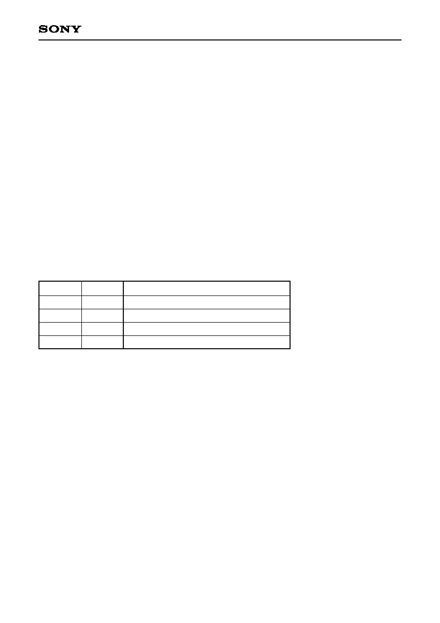
≠ 85 ≠
CXD1818R
2-4. Category 10 Commands
This commands can be executed only in the target mode status. If these commands are executed in any other
status, a CMDIGNR interrupt is generated. Commands for targets can be broadly classified into three groups.
a) Phase unit of transfer commands
b) Disconnect commands
c) Terminate I/O commands
2-4-1. Single phase of transfer commands
Single phase transfer commands include the following commands.
a) Receive data (80h)
b) Send data (81h)
c) Receive command (84h)
d) Send status (85h)
e) Receive message (86h)
f) Send message (87h)
g) Receive command sequence (8Ch)
These commands execute the transfer phase of the corresponding name. Each transfer command has three
modes. The mode is determined by the combination of the command's BUF (bit 5) and SUB (bit 4) bits.
BUF
0
0
1
1
0
1
0
1
Sub CPU ≠ SCSI 1-byte transfer
Sub CPU ≠ SCSI n-byte transfer (n = 1 to 16)
Buffer ≠ SCSI transfer
Undefined
SUB
Mode
a) Sub CPU ≠ SCSI 1-byte transfer
1) From the sub CPU to the SCSI:
The sub CPU must write the data to be transferred in the FIFO beforehand.
2) From the SCSI to the sub CPU:
If the command is executed, one byte of data enters the FIFO when a FUNCCMPL interrupt occurs.
b) Sub CPU ≠ SCSI n-byte transfer (n = 1 to 16)
1) From the sub CPU to the SCSI:
The sub CPU must write the data to be transferred in the FIFO beforehand.
2) From the SCSI to the sub CPU:
The number of bytes to be received must be written in the SXFRC register (58h) before issuing the
command. The maximum number of bytes which can be transferred with a single transfer is 16.
If the command is executed, data enters the FIFO when a FUNCCMPL interrupt occurs. At this time, the
number of bytes remaining to be transferred can be known by reading the SXFRC register (58h). If the
transfer is not interrupted by an SCSI parity error or the ATN condition, this value is "0".
c) Buffer ≠ SCSI transfer
The command is issued after setting the transfer at the decoder block side. Data can also be written in the
FIFO beforehand.

≠ 86 ≠
CXD1818R
(1) Receive command sequence (8Ch)
Description: The CDB is analyzed and received in the command phase.
Note) This command should be executed only when not even a single byte has been received yet in the
command phase.
Preparation: A number of operations must be performed before issuing this command.
1) Set the number of bytes when receiving a command from a command group which is undefined
by SCSI standards with the SCCDBSIZ register (69h).
Operation:
After shifting to the command phase, six CDB bytes are received unconditionally. After that, the
first CDB byte is analyzed, command group identification is performed and the number of deficient
bytes is received.
Interrupt:
FUNCCMPL
Function complete (INTSTS2 register (72h), bit 7)
Microcode status:
The microcode status has no meaning with this command.
2-4-2. Disconnect commands
These commands are issued in order to release the bus when the CXD1818R/SCSI2 core has completed a
series of operations as the target.
(1) Disconnect (88h)
Description: This command releases the SCSI bus in accordance with SCSI standards and sets the SCSI bus
to Bus-Free status.
Interrupt:
FUNCCMPL
Function complete (INTSTS2 register (72h), bit 7)
Microcode status:
The microcode status has no meaning with this command.
(2) Send Message(s) and Disconnect (89h)
Description: This command executes the Message In phase and then disconnects.
Preparation: A number of operations must be performed before issuing this command.
1) Set the FIFO to empty status with the Flush FIFO command and then write the message to be
transferred in Message In phase in the FIFO.
Operation:
After shifting to the Message In phase and transferring the FIFO data, the CXD1818R/SCSI2 core
is set to the disable selection status. Then the Bus-Free status is established, a FUNCCMPL
interrupt is generated and the command is completed.
Interrupt:
FUNCCMPL
Function complete (INTSTS2 register (72h), bit 7)
Microcode status:
The microcode status has no meaning with this command.
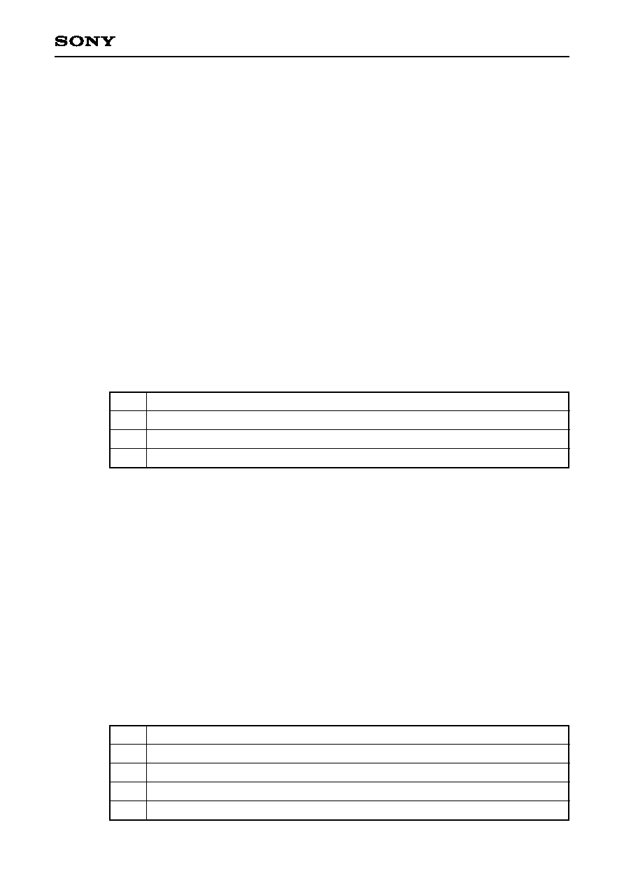
≠ 87 ≠
CXD1818R
2-4-3. Terminate I/O commands
These commands are issued in order to release the bus when the CXD1818R/SCSI2 core has completed a
series of operations as the target.
(1) Terminate I/O and Bus-Free (8Ah)
Description: After transferring one byte of the status in the Status phase, operation shifts to the Message In
phase and the message is transferred to the initiator. Then, the connection is disconnected and
the SCSI bus is set to Bus-Free status.
Preparation: A number of operations must be performed before issuing this command.
1) Set the FIFO to empty status with the Flush FIFO command and then write the one byte to be
transferred in the Status phase and the message to be transferred in the Message In phase in
the FIFO.
Operation:
After shifting to the Status phase and transferring one byte of the FIFO data, operation shifts to
the Message In phase and the FIFO data is transferred. Upon completion of the transfer, the
CXD1818R/SCSI2 core is set to the disable selection status. Then Bus-Free status is established,
a FUNCCMPL interrupt is generated and the command is completed.
Interrupt:
FUNCCMPL
Function complete (INTSTS2 register (72h), bit 7)
Microcode status:
The microcode status value when the command is completed has the following meanings.
Code
00h
01h
02h
Completed normally.
The ATN condition was established while executing the Status phase.
The ATN condition was established while executing the Message In phase.
Description
(2) Terminate I/O and link (8Bh)
Description: After transferring one byte of the status in the Status phase, operation shifts to the Message In
phase and the message is transferred to the initiator. Then, operation shifts to the command
phase, the SCSI CDB is received, and the command is completed.
Preparation: A number of operations must be performed before issuing this command.
1) Set the FIFO to the empty status with the Flush FIFO command and then write the one byte to
be transferred in the Status phase and the message to be transferred in the Message In phase
in the FIFO.
Operation:
After shifting to the Status phase and transferring one byte of the FIFO data, operation shifts to
the Message In phase and the FIFO data is transferred. Then, operation shifts to the command
phase, the CDB is received, a FUNCCMPL interrupt is generated and the command is completed.
Interrupt:
FUNCCMPL
Function complete (INTSTS2 register (72h), bit 7)
Microcode status:
The microcode status value when the command is completed has the following meanings.
Code
00h
01h
02h
03h
Completed normally.
The ATN condition was established while executing the Status phase.
The ATN condition was established while executing the Message In phase.
Operation shifted to the command phase after completing terminate I/O processing.
Description

≠ 88 ≠
CXD1818R
2-5. Category 11 Commands
These commands are stream commands, and can be executed anytime as long as a different command is not
currently being executed.
Terminology
1) Completed
Completed has the following meaning with stream processing.
Streams being executed cannot be reopened when they are completed.
Streams are completed when processing finishes normally. Streams can also be completed when they are
in interrupted state.
2) Interrupted
Interrupted has the following meaning with stream processing.
Streams are interrupted if the ATN condition is established, Reselection fails, or the CXD1818R responds to
a selection while executing the stream. Streams being executed can be reopened when they are in
interrupted state.
2-5-1. Stream abort
Description: Stream processing is forcibly completed.
Preparation: Before this command is issued, any one of the following conditions must be met.
a) The stream is interrupted by the ATN condition.
b) The stream is interrupted because Reselection failed.
c) The stream is interrupted because the CXD1818R responded to a selection.
d) The stream is interrupted after executing the stream pause command.
Operation:
After internally resetting the stream related circuits, a FUNCCMPL interrupt is generated and the
command is completed.
Interrupt:
FUNCCMPL
Function complete (INTSTS2 register (72h), bit 7)
Microcode status:
The microcode status has no meaning with this command.
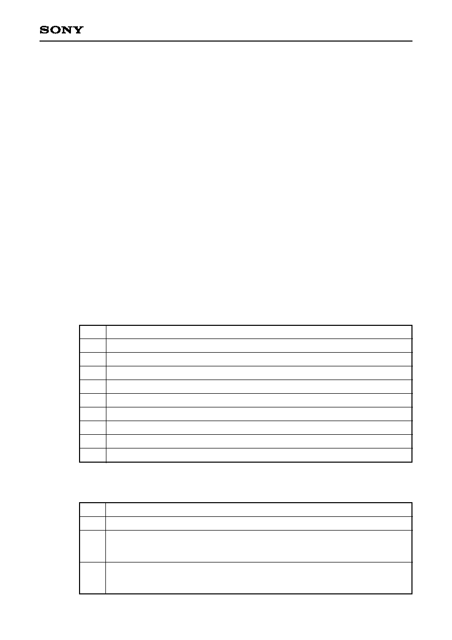
≠ 89 ≠
CXD1818R
Code
00h
01h
02h
03h
04h
05h
06h
07h
08h
Completed normally.
The CXD1818R was selected and an error occurred in the Message In phase.
The CXD1818R was selected and operation shifted to the command phase.
Reselection failed.
The ATN condition was established in the Message In phase immediately after Reselection.
The ATN condition was established in the Data In phase.
The ATN condition was established in the Message In phase during Disconnect.
The ATN condition was established in the Status phase during terminate I/O.
The ATN condition was established in the Message In phase during terminate I/O.
Description
2-5-2. Stream and stop (C1h)
Description: The stream command is executed.
Preparation: A number of operations must be performed before issuing this command.
1) Specify the CXD1818R operation with the SCCONF0 (60h), SCCONF1 (61h) and SCCONF2
(62h) registers.
2) Specify Disconnect allowed/not allowed and the operation when the ATN condition is
established with the SCSTCONF register.
3) Write the message to be transferred in the Message In phase immediately after Reselection,
and the data to be transferred in the status and Message In phases of the terminate I/O
sequence beforehand in the SCSTRSLM, SCSTTIOS and SCSTTIOM registers, respectively.
4) Prepare for auto transfer on the decoder block side.
Operation:
When Disconnect is allowed, the following sequences are executed.
a) The following sequence is executed each time the buffer data reaches the buffer full ratio
during transfer.
Reselection
Message In
Data In
Message In
Disconnect
b) The following sequence is executed only during the final connection.
Reselection
Message In
Data In
When Disconnect is not allowed, the following sequence is executed.
a) Data In
Interrupt:
FUNCCMPL
Function complete (INTSTS2 register (72h), bit 7)
Microcode status:
The microcode status value when the command is completed has the following meanings.
The meaning of each code after the stream pause command (C4h) has been issued is basically
the same. However, the meaning of the following codes changes slightly.
Code
Description
00h
04h
05h
Completed normally. However, the stream is interrupted.
The ATN condition was established in the Message In phase immediately after Reselection.
When the ATN condition is not established, the data to be transferred has already been
transferred and the stream is interrupted.
The ATN condition was established in the Data In phase.
When the ATN condition is not established, the data to be transferred has already been
transferred and the stream is interrupted.
≠ 90 ≠
CXD1818R
2-5-3. Stream and Bus-Free (C2h)
Description: The stream command is executed.
Preparation: A number of operations must be performed before issuing this command.
1) Specify the CXD1818R operation with the SCCONF0 (60h), SCCONF1 (61h) and SCCONF2
(62h) registers.
2) Specify Disconnect allowed/not allowed and the operation when the ATN condition is
established with the SCSTCONF register.
3) Write the message to be transferred in the Message In phase immediately after Reselection,
and the data to be transferred in the status and Message In phases of the terminate I/O
sequence beforehand in the SCSTRSLM, SCSTTIOS and SCSTTIOM registers, respectively.
4) Prepare for auto transfer on the decoder block side.
Operation:
When Disconnect is allowed, the following sequences are executed.
a) The following sequence is executed each time the buffer data reaches the buffer full ratio
during transfer.
Reselection
Message In
Data In
Message In
Disconnect
b) The following sequence is executed only during the final connection.
Reselection
Message In
Data In
Status
Message In
Bus-Free
When Disconnect is not allowed, the following sequence is executed.
a) Data In
Status
Message In
Bus-Free
Interrupt:
FUNCCMPL
Function complete (INTSTS2 register (72h), bit 7)
Microcode status:
The microcode status value when the command is completed has the following meanings.
Code
00h
01h
02h
03h
04h
05h
06h
07h
08h
Completed normally.
The CXD1818R was selected and an error occurred in the Message In phase.
The CXD1818R was selected and operation shifted to the command phase.
Reselection failed.
The ATN condition was established in the Message In phase immediately after Reselection.
The ATN condition was established in the Data In phase.
The ATN condition was established in the Message In phase during Disconnect.
The ATN condition was established in the Status phase during terminate I/O.
The ATN condition was established in the Message In phase during terminate I/O.
Description
The meaning of each code after the stream pause command (C4h) has been issued is basically
the same. However, the meaning of the following codes changes slightly.
Code
Description
00h
04h
05h
Completed normally. However, the stream is interrupted.
The ATN condition was established in the Message In phase immediately after Reselection.
When the ATN condition is not established, the data to be transferred has already been
transferred and the stream is interrupted.
The ATN condition was established in the Data In phase.
When the ATN condition is not established, the data to be transferred has already been
transferred and the stream is interrupted.

≠ 91 ≠
CXD1818R
Code
00h
01h
02h
03h
04h
05h
06h
07h
08h
09h
Completed normally.
The CXD1818R was selected and an error occurred in the Message In phase.
The CXD1818R was selected and operation shifted to the command phase.
Reselection failed.
The ATN condition was established in the Message In phase immediately after Reselection.
The ATN condition was established in the Data In phase.
The ATN condition was established in the Message In phase during Disconnect.
The ATN condition was established in the Status phase during terminate I/O.
The ATN condition was established in the Message In phase during terminate I/O.
Operation shifted to the command phase after executing terminate I/O processing.
Description
2-5-4. Stream and link (C3h)
Description: The stream command is executed.
Preparation: A number of operations must be performed before issuing this command.
1) Specify the CXD1818R operation with the SCCONF0 (60h), SCCONF1 (61h) and SCCONF2
(62h) registers.
2) Specify Disconnect allowed/not allowed and the operation when the ATN condition is
established with the SCSTCONF register.
3) Write the message to be transferred in the Message In phase immediately after Reselection,
and the data to be transferred in the status and Message In phases of the terminate I/O
sequence beforehand in the SCSTRSLM, SCSTTIOS and SCSTTIOM registers, respectively.
4) Prepare for auto transfer on the decoder block side.
Operation:
The following sequences are executed.
a) The following sequence is executed each time the buffer data reaches the buffer full ratio
during transfer.
Reselection
Message In
Data In
Message In
Disconnect
b) The following sequence is executed only during the final connection.
Reselection
Message In
Data In
Status
Message In
Command
When Disconnect is not allowed, the following sequence is executed.
a) Data In
Status
Message In
Command
Interrupt:
FUNCCMPL
Function complete (INTSTS2 register (72h), bit 7)
Microcode status:
The microcode status value when the command is completed has the following meanings.
The meaning of each code after the stream pause command (C4h) has been issued is basically
the same. However, the meaning of the following codes changes slightly.
Code
Description
04h
05h
09h
The ATN condition was established in the Message In phase immediately after Reselection.
When the ATN condition is not established, the data to be transferred has already been
transferred and the stream is interrupted.
ATN condition was established in the Data In phase.
When the ATN condition is not established, the data to be transferred has already been
transferred and the stream is interrupted.
Operation shifted to the command phase after executing terminate I/O processing.
However, the stream is interrupted.

≠ 92 ≠
CXD1818R
2-5-5. Stream pause (C4h)
Description: The stream command is interrupted.
This command is executed when the stream is to be interrupted for any reason other than SCSI
related factor. For example, upon seek error.
Preparation: This command can be issued anytime while executing the stream command.
Operation:
Operation switches to a mode which transfers all transferable data. An interrupt is not generated.
After all transferable data has been transferred, the stream command being executed generates a
FUNCCMPL interrupt and the command is completed.
Stream commands being executed when the stream pause command is issued perform the
following operations.
a) When the stream pause command is issued while executing the Data In phase:
After all transferable data has been transferred, a FUNCCMPL interrupt is generated and the
command is completed.
b) When the stream pause command is issued in the Bus-Free condition:
Reselection and the Message In phase are executed regardless of the values of BFFLRT and
BFBLKC. If there is transferable data, the Data In phase is executed, a FUNCCMPL interrupt is
generated and the command is completed.
The ATN condition following the issue of the stream pause command is processed normally.
Interrupt:
An interrupt is not generated for this command.
After this command is issued, an interrupt is generated for stream commands which are being
executed at that point when these streams are interrupted or completed. See the description of
each command for details.
Microcode status:
The microcode status conforms to the stream commands being executed when the stream pause
command is issued.

≠ 93 ≠
CXD1818R
[3] Appendix A
3-1. List of CD-ROM Decoder Block Registers
3-1-1. CD-ROM decoder block read registers
Sub CPU read registers (1)
00h
01h
02h
03h
04h
05h
06h
07h
08h
09h
0Ah
0Bh
0Ch
0Dh
0Eh
0Fh
10h
11h
12h
13h
14h
15h
16h
17h
18h
19h
b7
b7
b7
b7
b7
b7
b7
b7
b7
b7
b7
b7
MIN
UTE
MIN
UTE
SHRT
SCT
CMD
FM
b7
b7
1024
XFR
ENBL
KEFL
AUTO
DIST
ENSB
QRD
REV#
2
b7
b6
b6
b6
b6
b6
b6
b6
b6
b6
b6
b6
b6
SEC
OND
SEC
OND
NO
SYNC
b6
b6
512
XFR
BLKE
FLSL
MODE
SEL
ESPB
QRD
REV#
1
b6
b5
b5
b5
b5
b5
b5
b5
b5
b5
b5
b5
b5
BLO
CK
BLO
CK
COR
INH
b5
b5
SYNC
ENBY
TFBT
FORM
SEL
DEC
CMD2
REV#
0
b5
b4
b4
b4
b4
b4
b4
b4
b4
b4
b4
b4
b4
MODE
MODE
ERIN
BLK
b4
b4
HEAD
ER
BYTE
FLSL
ATTG
TMET
DEC
CMD1
b4
b3
b3
b3
b3
b3
b3
b3
b3
b3
b3
b3
b3
FILE
COR
DONE
b3
b3
SBHE
ADER
ENSB
CBT
ENFM
2EDC
DEC
CMD0
CMDO
BUSY
b3
b2
b2
b2
b2
b2
b2
b2
b2
b2
b2
b2
b2
CHAN
NEL
EDC
NG
EDC
ALL0
b2
b2
USER
DATA
ALL
SBC
MDBY
TCTL
ATW
SCTI
b2
b1
b1
b1
b1
b1
b1
b1
b1
b1
b1
b1
b1
SUB
MODE
ECC
NG
C
MODE
b1
b1
PARI
TY
SBCE
STS
EN
DLA
NTCR
CT1
CBFW
RRDY
b1
b0
b0
b0
b0
b0
b0
b0
b0
b0
b0
b0
b0
CDR
DTEN
DATA
TYPE
TGTN
TMET
C
FORM
b8
b0
b8
b0
AUTO
XFR
ZA
SQEF
ATDL
RNEW
NTCR
CT0
CBFR
DRDY
b0
Adr.
bit7
bit6
bit5
bit4
bit3
bit2
bit1
bit0
Reg.
RAWMIN
RAWSEC
RAWBLK
RAWMD
BFMIN
BFSEC
BFHDRBLK
BFMD
BFFILE
BFCHAN
BFSUBM
BFDTYP
RAWHDR
FLG
BFHDR
FLG
DECSTS
0
DECSTS
1
LSTARA-H
LSTARA-L
LHADR-H
LHADR-L
XFRFMT
0
XFRFMT
1
DECCTL
0
DECCTL
1
XFRSTS
CPUBRDT

≠ 94 ≠
CXD1818R
Sub CPU read registers (2)
1Ah
1Bh
1Ch
1Dh
1Eh
1Fh
20h
21h
22h
23h
24h
25h
26h
27h
28h
29h
2Ah
2Bh
2Ch
2Dh
2Eh
2Fh
30h
31h
32h
33h
34h
35h
36h
37h
38h
39h
3Ah
SUBQ
FMSL
SBC
OVRN
SBQ
ERR
b7
b7
b7
b7
b7
b7
b7
b23
b15
b7
b7
b15
b7
b15
b7
OVER
FLOW
b6
b6
b6
b6
b6
b6
b6
b22
b14
b6
b6
b14
b6
b14
b6
BFNT
VAL
b5
b5
b5
b5
b5
b5
b5
b21
b13
b5
b5
b13
b5
b13
b5
NO
SYNC
b4
b4
b4
b4
b4
b4
b4
b20
b12
b4
b4
b12
b4
b12
b4
SBC
ERR3
b3
b3
b3
b3
b3
b3
b3
b19
b11
b3
b3
b19
b11
b3
b19
b11
b3
MODE
2
SBC
ERR2
SHTS
BCS
INCB
LKS2
b2
PACK
MODE
b2
b2
b2
b2
b2
b2
b18
b10
b2
b2
b18
b10
b2
b18
b10
b2
FORM
2
SBC
ERR1
NOSY
NC
INCB
LKS1
b1
b1
b1
b1
b1
b1
b1
b17
b9
b1
b1
XFR
POS1
b17
b9
b1
b17
b9
b1
XFR
SCT
SBC
ERR0
SUBQ
ERR
INCB
LKS0
b0
b8
b0
b8
b0
b8
b0
b0
b0
b0
b16
b8
b0
b8
b0
XFR
POS0
b16
b8
b0
b16
b8
b0
Adr.
bit7
bit6
bit5
bit4
bit3
bit2
bit1
bit0
Reg.
SCTINF
SBCSTS
SBQSTS
INC
BLKS
SBQDT
CHPCTL
1
BFARA#-H
BFARA#-L
CSCTARA-H
CSCTARA-L
DLARA-H
DLARA-L
TGTMIN
TGTSEC
TGTBLK
XFRCNT-H
XFRCNT-M
XFRCNT-L
XFRARA-H
XFRARA-L
XFRPOS
HXFRC-H
HXFRC-M
HXFRC-L
HADRC-H
HADRC-M
HADRC-L

≠ 95 ≠
CXD1818R
Sub CPU read registers (3)
3Bh
3Ch
3Dh
3Eh
3Fh
40h
41h
42h
43h
44h
45h
46h
47h
48h
49h
4Ah
4Bh
4Ch
4Dh
4Eh
4Fh
b15
b7
b15
b7
b15
b7
b7
b7
b15
b7
b7
b7
b14
b6
b14
b6
b14
b6
b6
b6
b14
b6
b6
b6
b13
b5
b13
b5
b13
b5
b5
b5
b13
b5
b5
b5
b12
b4
b12
b4
b12
b4
b4
b4
b12
b4
b4
b4
b19
b11
b3
b19
b11
b3
b19
b11
b3
b3
b3
b11
b3
b3
b3
b18
b10
b2
b18
b10
b2
b18
b10
b2
b2
b2
b10
b2
b2
b2
b17
b9
b1
b17
b9
b1
b17
b9
b1
b9
b1
b9
b1
b9
b1
b1
b1
b16
b8
b0
b16
b8
b0
b16
b8
b0
b8
b0
b8
b0
b8
b0
b0
b8
b0
Adr.
bit7
bit6
bit5
bit4
bit3
bit2
bit1
bit0
Reg.
SLADR-H
SLADR-M
SLADR-L
CWADRC-H
CWADRC-M
CWADRC-L
CRADRC-H
CRADRC-M
CRADRC-L
BFBLKC-H
BFBLKC-L
BFFLRT-H
BFFLRT-L
TIMER-H
TIMER-L
TMRRSL
ESPSBCAM
STARTARA-H
STARTARA-L

≠ 96 ≠
CXD1818R
3-1-2. CD-ROM decoder block write registers
Sub CPU write registers (1)
00h
01h
02h
03h
04h
05h
06h
07h
08h
09h
0Ah
0Bh
0Ch
0Dh
0Eh
0Fh
10h
11h
12h
13h
14h
15h
16h
17h
18h
19h
1Ah
1Bh
1Ch
CINT
POL
SW
OPEN
C2PO
L1st
b7
DSTB
SL1
b7
DLAR
NWMS
HCAS
CYCS
"L"
"L"
"L"
"L"
"L"
"L"
"L"
"L"
"L"
b7
"L"
b7
1024
XFR
ENBL
KEFL
AUTO
DIST
ENSB
QRD
CHIP
RST
b7
SUB
FMSL
b7
b7
RAM
SIZE1
SYC
NGC2
LCH
LOW
b6
DSTB
SL0
b6
SBAI
TMSL
DMA
CYC4
"L"
"L"
"L"
"L"
"L"
"L"
"L"
"L"
"L"
b6
"L"
b6
512
XFR
BLKE
FLSL
MODE
SEL
ESPB
CKMD
TGT
MET
b6
"L"
b6
b6
RAM
SIZE0
SYC
NGC1
BCH
RED
b5
DIS
XLAT
b5
"L"
DRQ
PRS
"L"
"L"
"L"
"L"
"L"
"L"
"L"
"L"
"L"
b5
"L"
b5
SYNC
ENBY
TFBT
FORM
SEL
DEC
CMD2
INC
TGT
b5
"L"
b5
b5
RAM8
BITW
SYC
NGC0
BCKL
MD1
b4
XFR
BYT1
b4
LRSEL
DRQ
PRS2
"L"
"L"
"L"
"L"
"L"
"L"
"L"
"L"
"L"
b4
"L"
b4
HEAD
ER
BYTE
FLSL
ATTG
TMET
DEC
CMD1
RPCO
RTRG
b4
"L"
b4
b4
RAM
2CAS
DCK
SEL
BCKL
MD0
b3
XFR
BYT0
b3
MMC
HWKR
QDIS
"L"
"L"
"L"
"L"
"L"
"L"
"L"
"L"
"L"
b3
"L"
b3
SBHE
ADER
ENSB
CBT
ENFM
2EDC
DEC
CMD0
BF
STOP
b3
"L"
b3
b3
"L"
"L"
LSB
1st
b2
FAST
DSTB
b2
CSCT
ASET
EDOD
RAM
"L"
"L"
"L"
"L"
"L"
"L"
"L"
"L"
"L"
b2
"L"
b2
USER
DATA
ALL
SBC
MDBY
TCTL
ATW
SCTI
CLDS
PCMD
b2
MODE
2
b2
b2
CLK
SEL1
SBC
ECC1
"L"
b1
EXCK
SEL1
b1
EDCT
OECC
EDCF
FEN
"L"
"L"
"L"
"L"
"L"
"L"
"L"
"L"
"L"
b1
"L"
b1
PARI
TY
SBCE
STS
EN
DLA
NTCR
CT1
DSPC
MDXF
b1
FORM
2
b1
b1
CLK
SEL0
SBC
ECC0
BFSH
DFSL
b0
EXCK
SEL0
b0
ASC
ON
ECAS
CYCS
"L"
"L"
"L"
"L"
CDR
DTEN
"L"
"L"
"L"
b8
b0
b8
b0
AUTO
XFR
ZA
SQEF
ATDL
RNEW
NTCR
CT0
DSPC
MDLT
b0
XFR
SCT
b0
b0
Adr.
bit7
bit6
bit5
bit4
bit3
bit2
bit1
bit0
Reg.
CONFIG0
CONFIG1
DSPIF
RFINTVL
DSPCTL
DSPCMD
CONFIG2
DMACTL
CDRMOD
LSTARA-H
LSTARA-L
LHADR-H
LHADR-L
XFRFMT
0
XFRFMT
1
DECCTL
0
DECCTL
1
CHPCTL
0
CPUBWDT
SCTINF
BLKESTS
SBCESTS

≠ 97 ≠
CXD1818R
Sub CPU write registers (2)
1Dh
1Eh
1Fh
20h
21h
22h
23h
24h
25h
26h
27h
28h
29h
2Ah
2Bh
2Ch
2Dh
2Eh
2Fh
30h
31h
32h
33h
34h
35h
36h
37h
38h
39h
3Ah
3Bh
3Ch
3Dh
3Eh
3Fh
"L"
b7
PSA
V3
"L"
b7
"L"
"L"
"L"
b7
"L"
b7
b7
b7
"L"
b23
b15
b7
"L"
b7
"L"
"L"
"L"
"L"
b15
b7
"L"
"L"
b15
b7
"L"
"L"
b15
b7
"L"
"L"
"L"
b6
"L"
"L"
b6
"L"
"L"
"L"
b6
"L"
b6
b6
b6
"L"
b22
b14
b6
"L"
b6
"L"
"L"
"L"
"L"
b14
b6
"L"
"L"
b14
b6
"L"
"L"
b14
b6
"L"
"L"
"L"
b5
PSA
V1
"L"
b5
"L"
"L"
"L"
b5
"L"
b5
b5
b5
"L"
b21
b13
b5
"L"
b5
"L"
"L"
"L"
"L"
b13
b5
"L"
"L"
b13
b5
"L"
"L"
b13
b5
"L"
"L"
"L"
b4
PSA
V0
"L"
b4
"L"
"L"
"L"
b4
"L"
b4
b4
b4
"L"
b20
b12
b4
"L"
b4
"L"
"L"
"L"
"L"
b12
b4
"L"
"L"
b12
b4
"L"
"L"
b12
b4
"L"
"L"
"L"
b3
"L"
"L"
b3
"L"
"L"
"L"
b3
"L"
b3
b3
b3
"L"
b19
b11
b3
"L"
b3
"L"
"L"
"L"
b19
b11
b3
"L"
b19
b11
b3
"L"
b19
b11
b3
"L"
b19
INCB
LKS2
b2
PACK
MODE
"L"
b2
"L"
"L"
"L"
b2
"L"
b2
b2
b2
"L"
b18
b10
b2
"L"
b2
IGNXF
RSCT
"L"
"L"
b18
b10
b2
"L"
b18
b10
b2
"L"
b18
b10
b2
"L"
b18
INCB
LKS1
b1
"L"
"L"
b1
"L"
"L"
"L"
b1
"L"
b1
b1
b1
"L"
b17
b9
b1
"L"
b1
IGNXF
RFST
XFR
POS1
"L"
b17
b9
b1
"L"
b17
b9
b1
"L"
b17
b9
b1
"L"
b17
INCB
LKS0
b0
"L"
b8
b0
"L"
"L"
b8
b0
"L"
b0
b0
b0
"L"
b16
b8
b0
b8
b0
XSOS
TOP
XFR
POS0
"L"
b16
b8
b0
"L"
b16
b8
b0
"L"
b16
b8
b0
"L"
b16
Adr.
bit7
bit6
bit5
bit4
bit3
bit2
bit1
bit0
Reg.
INC
BLKS
BYTERSTS
CHPCTL
1
BFARA#-H
BFARA#-L
DLARA-H
DLARA-L
TGTMIN
TGTSEC
TGTBLK
XFRCNT-H
XFRCNT-M
XFRCNT-L
XFRARA-H
XFRARA-L
XFRCTL
XFRPOS
HXFRC-H
HXFRC-M
HXFRC-L
HADRC-H
HADRC-M
HADRC-L
SLADR-H
SLADR-M
SLADR-L
CWADRC-H

≠ 98 ≠
CXD1818R
Sub CPU write registers (3)
40h
41h
42h
43h
44h
45h
46h
47h
48h
49h
4Ah
4Bh
4Ch
b15
b7
"L"
"L"
b15
b7
"L"
b7
"L"
b7
b15
b7
b7
b14
b6
"L"
"L"
b14
b6
"L"
b6
"L"
b6
b14
b6
b6
b13
b5
"L"
"L"
b13
b5
"L"
b5
"L"
b5
b13
b5
b5
b12
b4
"L"
"L"
b12
b4
"L"
b4
"L"
b4
b12
b4
b4
b11
b3
"L"
b19
b11
b3
"L"
b3
"L"
b3
b11
b3
b3
b10
b2
"L"
b18
b10
b2
"L"
b2
"L"
b2
b10
b2
b2
b9
b1
"L"
b17
b9
b1
b9
b1
b9
b1
b9
b1
b1
b8
b0
"L"
b16
b8
b0
b8
b0
b8
b0
b8
b0
b0
Adr.
bit7
bit6
bit5
bit4
bit3
bit2
bit1
bit0
Reg.
CWADRC-M
CWADRC-L
CRADRC-H
CRADRC-M
CRADRC-L
BFBLKC-H
BFBLKC-L
BFFLRT-H
BFFLRT-L
TIMER-H
TIMER-L
TMRRSL

≠ 99 ≠
CXD1818R
3-2. List of SCSI Controller Block Registers
3-2-1. SCSI controller block read registers
List of SCSI2 controller block read registers (1)
50h
51h
52h
53h
54h
55h
56h
57h
58h
59h
5Ah
5Bh
5Ch
5Dh
5Eh
5Fh
MON
RST
MON
BSY
FIFE
MPTY
B07
"L"
SYXF
RPD3
CTL
BSY
MON
DBP
MON
SEL
B06
"L"
SYXF
RPD2
CTL
SEL
MON
MSG
B05
"L"
SYXF
RPD1
CTL
MSG
MON
CD
FIF
FULL
B04
B04
SYXF
RPD0
CTL
CD
TAPE
MODE
MON
IO
FIF
CNT3
B03
B03
SYXF
ROF3
CTL
IO
TBC
ZERO
MON
REQ
FIF
CNT2
B02
B02
SYXF
ROF2
CTL
REQ
MON
ACK
FIF
CNT1
B01
B01
SYXF
ROF1
CTL
ACK
CMDI
NPRG
MON
ATN
FIF
CNT0
B00
B00
SYXF
ROF0
CTL
ATN
Adr.
bit7
bit6
bit5
bit4
bit3
bit2
bit1
bit0
Reg.
SCSTS
Reserved
Reserved
Reserved
SCSCBMON
SCFIF
STS
Reserved
SCDATA
SCSXFRC
Reserved
Reserved
SCSYNCTL
Reserved
Reserved
SCSCBCTL
Reserved

≠ 100 ≠
CXD1818R
List of SCSI2 controller block read registers (2)
60h
61h
62h
63h
64h
65h
66h
67h
68h
69h
69h
6Ah
6Bh
6Ch
6Dh
6Eh
6Fh
FAST
SCSI
RSLT
OUT7
SEL
ID2
GP7
B1
GP7
B1
USTS
B7
RSLM
SG7
TIOS
TS7
TIOM
SG7
HSXF
RSPE
RSLT
OUT6
SEL
ID1
GP7
B0
GP7
B0
USTS
B6
RSLM
SG6
TIOS
TS6
TIOM
SG6
CDBS
IZDF
HSXF
RAT
RSLT
OUT5
SEL
ID0
GP6
B1
GP6D
B1
USTS
B5
RSLM
SG5
TIOS
TS5
TIOM
SG5
ANEG
DATA
HSL
SPE
RSLT
OUT4
SELI
DINV
GP6
B0
GP6D
B0
USTS
B4
RSLM
SG4
TIOS
TS4
TIOM
SG4
ANEG
RQAK
RSL
RTC3
RSLT
OUT3
GP4
B1
GP6C
B1
USTS
B3
RSLM
SG3
TIOS
TS3
TIOM
SG3
ATNA
RSD
RSL
RTC2
RSLT
OUT2
OWN
ID2
GP4
B0
GP6C
B0
USTS
B2
STDS
CPRV
RSLM
SG2
TIOS
TS2
TIOM
SG2
ATN
STP
RSL
RTC1
IDAS
SIGN
RSLT
OUT1
OWN
ID1
GP3
B1
GP43
B1
USTS
B1
RSLM
SG1
TIOS
TS1
TIOM
SG1
ULTRA
SCSI
RSL
RTC0
IDUN
ASGN
RSLT
OUT0
OWN
ID0
GP3
B0
GP43
B0
USTS
B0
RSLM
SG0
TIOS
TS0
TIOM
SG0
Adr.
bit7
bit6
bit5
bit4
bit3
bit2
bit1
bit0
Reg.
SCCONF0
SCCONF1
SCCONF2
SCRSLTOT
Reserved
SCID
Reserved
Reserved
Reserved
SCCDBSIZ
CDBSIZDF=0
SCCDBSIZ
CDBSIZDF=1
SC
USTS
SCSTCONF
SCSTRSLM
SCSTTIOS
SCSTTIOM
Reserved

≠ 101 ≠
CXD1818R
3-2-2. SCSI controller block write registers
List of SCSI2 controller block write registers (1)
50h
51h
52h
53h
54h
55h
56h
57h
58h
59h
5Ah
5Bh
5Ch
5Dh
5Eh
5Fh
CAT1
B07
B07
SYXF
RPD3
CTL
BSY
CAT0
B06
B06
SYXF
RPD2
CTL
SEL
B05
B05
B05
SYXF
RPD1
CTL
MSG
B04
B04
B04
SYXF
RPD0
CTL
CD
B03
B03
B03
SYXF
ROF3
CTL
IO
B02
B02
B02
SYXF
ROF2
CTL
REQ
B01
B01
B01
SYXF
ROF1
CTL
ACK
B00
B00
B00
SYXF
ROF0
CTL
ATN
Adr.
bit7
bit6
bit5
bit4
bit3
bit2
bit1
bit0
Reg.
SCCMD
Reserved
Reserved
Reserved
Reserved
Reserved
Reserved
SCDATA
SCSXFRC
Reserved
Reserved
SCSYNCTL
Reserved
Reserved
SCSCBCTL
Reserved

≠ 102 ≠
CXD1818R
List of SCSI2 controller block write registers (2)
60h
61h
62h
63h
64h
65h
66h
67h
68h
69h
69h
6Ah
6Bh
6Ch
6Dh
6Eh
6Fh
FAST
SCSI
RSLT
OUT7
SEL
ID2
GP7
B1
GP7
B1
RSLM
SG7
TIOS
TS7
TIOM
SG7
HSXF
RSPE
RSLT
OUT6
SEL
ID1
GP7
B0
GP7
B0
RSLM
SG6
TIOS
TS6
TIOM
SG6
CDBS
IZDF
HSXF
RAT
RSLT
OUT5
SEL
ID0
GP6
B1
GP6D
B1
RSLM
SG5
TIOS
TS5
TIOM
SG5
ANEG
DATA
SPAR
ENB
RSLT
OUT4
GP6
B0
GP6D
B0
RSLM
SG4
TIOS
TS4
TIOM
SG4
ANEG
RQAK
RSL
RTC3
RSLT
OUT3
GP4
B1
GP6C
B1
RSLM
SG3
TIOS
TS3
TIOM
SG3
ATNA
RSD
RSL
RTC2
RSLT
OUT2
OWN
ID2
GP4
B0
GP6C
B0
STDS
CPRV
RSLM
SG2
TIOS
TS2
TIOM
SG2
ATN
STP
RSL
RTC1
IDAS
SIGN
RSLT
OUT1
OWN
ID1
GP3
B1
GP43
B1
RSLM
SG1
TIOS
TS1
TIOM
SG1
ULTRA
SCSI
RSL
RTC0
IDUN
ASGN
RSLT
OUT0
OWN
ID0
GP3
B0
GP43
B0
RSLM
SG0
TIOS
TS0
TIOM
SG0
Adr.
bit7
bit6
bit5
bit4
bit3
bit2
bit1
bit0
Reg.
SCCONF0
SCCONF1
SCCONF2
SCRSLTOT
Reserved
SCID
Reserved
Reserved
Reserved
SCCDBSIZ
CDBSIZDF=0
SCCDBSIZ
CDBSIZDF=1
Reserved
SCSTCONF
SCSTRSLM
SCSTTIOS
SCSTTIOM
Reserved

≠ 103 ≠
CXD1818R
3-3. List of Common Registers
3-3-1. Common read registers
70h
71h
72h
73h
74h
75h
76h
77h
78h
79h
7Ah
7Bh
7Ch
7Dh
7Eh
7Fh
DEC
INT
FUNC
CMPL
DEC
INT
FUNC
CMPL
ROF
BFSH
DRFLG
DEC
TOUT
CMD
IGNR
DEC
TOUT
DIS
CNCT
BMF
UL
EDC
ALLO
DRV
OVRN
SCSI
RST
DRV
OVRN
SCSI
RST
BFE
MP
COR
INH
CRST
END
ATN
COND
CRCT
END
ATN
COND
NOG
SCR
ERIN
BLK
CDR
INT
ESP
EMP
SCSI
PERR
CDR
INT
ESP
EMP
SCSI
PERR
ESPW
DEN
COR
DONE
ECCO
VRN
ESP
WINH
SLW
ATN
ESP
WINH
SLW
ATN
SCSI
REL
ESPR
DEN
EDC
NG
NOTA
TWSI
TIME
R
SLWO
ATN
SCAM
INIF
NOTA
TWSI
TIME
R
SLWO
ATN
SCAN
INIF
SCTM
REL
GROK
ECC
NG
C
MODE
SHT
SYNC
SUBC
SYNC
RSL
FAIL
SCAN
SL
SHT
SYNC
SUBC
SYNC
RSL
FAIL
SCAM
SL
DEC
REL
QVLD
TGTN
TMET
C
FORM
Adr.
bit7
bit6
bit5
bit4
bit3
bit2
bit1
bit0
Reg.
INTSTS0
INTSTS1
INTSTS2
INTSTS3
INTEN0
INTEN1
INTEN2
INTEN3
INTSRC
ESPARA
SUBBLKC-H
SUBBLKC-L
ESPSTS0
ESPSTS1
INTCOND0
INTCOND1

≠ 104 ≠
CXD1818R
3-3-2. Common write registers
70h
71h
72h
73h
74h
75h
76h
77h
78h
79h
7Ah
7Bh
7Ch
7Dh
7Eh
7Fh
DEC
TOUT
CMD
IGNR
DEC
TOUT
CMD
IGNR
"L"
"H"
EDC
ALLO
DEC
INT
FUNK
CMPL
DEC
INT
FUNK
CMPL
"L"
ESPA
RST
LSB1
ST
EDC
ALLO
DRV
OVRN
SCSI
RST
DRV
OVRN
SCSI
RST
BCK
FED
"H"
COR
INH
CRST
END
ATN
COND
CRCT
END
ATN
COND
SQOK
"H"
ERIN
BLK
CDR
INT
ESP
EMP
SCSI
PERR
CDR
INT
ESP
EMP
SCSI
PERR
ESPW
REN
"H"
COR
DONE
ECCO
VRN
ESP
WINH
SLW
ATN
ESP
WINH
SLW
ATN
ESPR
DEN
"H"
EDC
NG
NOTA
TWSI
TIME
R
SLWO
ATN
SCAM
INIF
NOTA
TWSI
TIME
R
SLWO
ATN
SCAN
INIF
ESP
RST
"H"
ECC
NG
C
MODE
SHT
SYNC
SUBC
SYNC
RSL
FAIL
SCAN
SL
SHT
SYNC
SUBC
SYNC
RSL
FAIL
SCAM
SL
GRST
"H"
TGTN
TMET
C
FORM
Adr.
bit7
bit6
bit5
bit4
bit3
bit2
bit1
bit0
Reg.
CLRINT0
CLRINT1
CLRINT2
CLRINT3
INTEN0
INTEN1
INTEN2
INTEN3
ESPARA
SUBBLKC-H
SUBBLKC-L
ESPCTL0
ESPCTL1
INTCOND0
INTCOND1
≠ 105 ≠
CXD1818R
3-4. Register Reset Conditions
XRST: XRST pin
CRST: bit 7 of the CHPCTL0 register (18h) -bit7
XRES: XRES pin
RCMD: Chip reset command
3-4-1. CD-ROM decoder block, ESP block register reset conditions
(1) Sub CPU write registers
Reg.
CONFIG0
CONFIG1
DSPIF
RFINTVL
DSPCTL
DSPCMD
CONFIG2
DMACTL
LSTARA-H
LSTARA-L
LHADR-H
LHADR-L
XFRFMT0
XFRFMT1
DECCTL0
DECCTL1
CHPCTL0
CPUBWDT
SCTINF
BLKESTS
SBCESTS
INCBLKS
BYTERSTS
CHPCTL1
BFARA-H
BFARA-L
DLARA-H
DLARA-L
TGTMNT
TGTSEC
TGTBLK
XFRCNT-H
Adr.
00h
01h
02h
03h
04h
05h
06h
07h
10h
11h
12h
13h
14h
15h
16h
17h
18h
19h
1Ah
1Bh
1Ch
1Dh
1Eh
1Fh
20h
21h
24h
25h
27h
28h
29h
2Bh
XRES
O
O
O
O
O
O
O
O
O
O
O
O
O
O
O
O
O
O
O
O
O
O
O
O
O
O
O
O
O
O
O
CRST
O
O
O
O
O
O
O
O
O
O
O
O
O
O
O
O
O
O
O
O
O
O
O
O
O
O
O
XRST RCMD
Bit 7 6 5 4 3 2 1 0
0 0 0 0 0 x 0 0
0 0 1 0 0 x 0 1
0 0 1 0 1 0 x 0
x x x x x x x x
0 0 0 1 1 0 1 1
0 0 0 0 0 0 0 0
0 1 x 0 0 0 0 0
1 0 1 1 1 0 0 0
x x x x x x x 0
0 0 0 0 0 0 0 0
x x x x x x x 0
0 0 0 0 0 0 0 0
0 0 0 0 0 0 0 1
0 0 0 0 0 0 0 0
1 0 0 0 0 1 0 1
0 0 0 0 0 0 0 0
0 0 0 0 0 0 0 0
0 0 0 0 0 0 0 0
x x x x x 0 0 0
0 0 0 0 0 0 0 0
0 0 0 0 0 0 0 0
x x x x x 0 0 1
0 0 0 0 0 0 0 0
0 x 0 0 x 1 x x
x x x x x x x 0
0 0 0 0 0 0 0 0
x x x x x x x 0
0 0 0 0 0 0 0 0
0 0 0 0 0 0 0 0
0 0 0 0 0 0 0 0
0 0 0 0 0 0 0 0
0 0 0 0 0 0 0 0

≠ 106 ≠
CXD1818R
Reg.
XFRCNT-M
XFRCNT-L
XFRARA-H
XFRARA-L
XFRCTL
XFRPOS
HXFRC-H
HXFRC-M
HXFRC-L
HADRC-H
HADRC-M
HADRC-L
SLADR-H
SLADR-M
SLADR-L
CWADRC-H
CWADRC-M
CWADRC-L
CRADRC-H
CRADRC-M
CRADRC-L
BFBLKC-H
BFBLKC-L
BFFLRT-H
BFFLRT-L
TIMER-H
TIMER-L
TMRRSL
CLRINT0
CLRINT1
INTEN0
INTEN1
ESPARA
SUBBLKC-H
SUBBLKC-L
ESPCTL0
ESPCTL1
INTCOND0
INTCOND1
Adr.
2Ch
2Dh
2Eh
2Fh
30h
31h
33h
34h
35h
37h
38h
39h
3Bh
3Ch
3Dh
3Fh
40h
41h
43h
44h
45h
46h
47h
48h
49h
4Ah
4Bh
4Ch
70h
71h
74h
75h
79h
7Ah
7Bh
7Ch
7Dh
7Eh
7Fh
XRES
O
O
O
O
O
O
O
O
O
O
O
O
O
O
O
O
O
O
O
O
O
O
O
O
O
O
O
O
O
O
O
O
O
O
O
O
O
O
O
CRST
O
O
O
O
O
O
O
O
O
O
O
O
O
O
O
O
O
O
O
O
O
O
O
O
O
O
O
O
O
O
O
O
O
O
O
O
O
O
O
XRST RCMD
Bit 7 6 5 4 3 2 1 0
0 0 0 0 0 0 0 0
0 0 0 0 0 0 0 0
x x x x x x x 0
0 0 0 0 0 0 0 0
x x x x x 0 0 0
x x x x x x 0 0
x x x x 0 0 0 0
0 0 0 0 0 0 0 0
0 0 0 0 0 0 0 0
x x x x 0 0 0 0
0 0 0 0 0 0 0 0
0 0 0 0 0 0 0 0
x x x x 0 0 0 0
0 0 0 0 0 0 0 0
0 0 0 0 0 0 0 0
x x x x 0 0 0 0
0 0 0 0 0 0 0 0
0 0 0 0 0 0 0 0
x x x x 0 0 0 0
0 0 0 0 0 0 0 0
0 0 0 0 0 0 0 0
x x x x x 0 0 0
0 0 0 0 0 0 0 0
x x x x x 0 0 0
0 0 0 0 0 0 0 1
0 0 0 0 0 0 0 0
0 0 0 0 0 0 0 0
1 1 1 1 1 0 1 0
0 0 0 0 0 0 0 0
x x x x 0 0 0 0
0 0 0 0 0 0 0 0
x x x x 0 0 0 0
x 0 0 0 0 0 0 0
x x x x x 0 0 0
0 0 0 0 0 0 0 0
0 0 0 0 0 0 0 0
0 0 0 0 0 0 0 0
0 0 0 0 0 0 0 0
x x x x x x 0 0

≠ 107 ≠
CXD1818R
(2) Sub CPU read registers
Reg.
RAWMIN
RAWSEC
RAWBLK
RAWMD
BFMIN
BFSEC
BFBLK
BFMD
BFFILE
BFCHAN
BFSUBM
BFDTYP
RAWHDFLG
BFHDRFLG
DECSTS0
DECSTS1
LSTARA-H
LSTARA-L
LHADR-H
LHADR-L
XFRFMT0
XFRFMT1
DECCTL0
DECCTL1
XFRSTS
CPUBRDT
SCTINF
SBCSTS
SBQSTS
INCBLKS
SUBQDT
CHPCTL1
BFARA-H
BFARA-L
CSCTAAR-H
CSCTAAR-L
Adr.
00h
01h
02h
03h
04h
05h
06h
07h
08h
09h
0Ah
0Bh
0Ch
0Dh
0Eh
0Fh
10h
11h
12h
13h
14h
15h
16h
17h
18h
19h
1Ah
1Bh
1Ch
1Dh
1Eh
1Fh
20h
21h
22h
23h
XRES
O
O
O
O
O
O
O
O
O
O
O
O
O
O
O
O
O
O
O
O
O
O
O
O
O
O
O
O
O
O
O
O
O
O
CRST
O
O
O
O
O
O
O
O
O
O
O
O
O
O
O
O
O
O
O
O
O
O
O
O
O
O
O
O
O
O
O
O
O
O
XRST RCMD
Bit 7 6 5 4 3 2 1 0
0 0 0 0 0 0 0 0
0 0 0 0 0 0 0 0
0 0 0 0 0 0 0 0
0 0 0 0 0 0 0 0
0 0 0 0 0 0 0 0
0 0 0 0 0 0 0 0
0 0 0 0 0 0 0 0
0 0 0 0 0 0 0 0
0 0 0 0 0 0 0 0
0 0 0 0 0 0 0 0
0 0 0 0 0 0 0 0
0 0 0 0 0 0 0 0
0 0 0 0 x x x x
0 0 0 0 0 0 0 0
0 0 0 0 0 0 0 0
x x x 0 0 0 0 0
x x x x x x x 0
0 0 0 0 0 0 0 0
x x x x x x x 0
0 0 0 0 0 0 0 0
0 0 0 0 0 0 0 1
0 0 0 0 0 0 0 0
1 0 0 x 0 1 0 1
0 0 0 0 0 x 0 0
0 0 0 x 0 x 1 0
x x x x x x x x
x x x x x 0 0 0
x x x x x x x x
x x x x x 0 0 0
x x x x x 0 0 1
x x x x x x x x
0 x 0 0 x 1 x x
x x x x x x x 0
0 0 0 0 0 0 0 0
x x x x x x x 0
0 0 0 0 0 0 0 0

≠ 108 ≠
CXD1818R
Reg.
DLARA-H
DLARA-L
TGTMNT
TGTSEC
TGTBLK
XFRCNT-H
XFRCNT-M
XFRCNT-L
XFRARA-H
XFRARA-L
XFRPOS
HXFRC-H
HXFRC-M
HXFRC-L
HADRC-H
HADRC-M
HADRC-L
SLADR-H
SLADR-M
SLADR-L
CWADRC-H
CWADRC-M
CWADRC-L
CRADRC-H
CRADRC-M
CRADRC-L
BFBLKC-H
BFBLKC-L
BFFLRT-H
BFFLRT-L
TIMER-H
TIMER-L
TMRRSL
ESPSBCAM
STAARA-H
STAARA-L
INTSTS0
INTSTS1
Adr.
24h
25h
27h
28h
29h
2Bh
2Ch
2Dh
2Eh
2Fh
31h
33h
34h
35h
37h
38h
39h
3Bh
3Ch
3Dh
3Fh
40h
41h
43h
44h
45h
46h
47h
48h
49h
4Ah
4Bh
4Ch
4Dh
4Eh
4Fh
70h
71h
XRES
O
O
O
O
O
O
O
O
O
O
O
O
O
O
O
O
O
O
O
O
O
O
O
O
O
O
O
O
O
O
O
O
O
O
O
O
O
O
CRST
O
O
O
O
O
O
O
O
O
O
O
O
O
O
O
O
O
O
O
O
O
O
O
O
O
O
O
O
O
O
O
O
O
O
O
O
O
O
XRST RCMD
Bit 7 6 5 4 3 2 1 0
x x x x x x x 0
0 0 0 0 0 0 0 0
0 0 0 0 0 0 0 0
0 0 0 0 0 0 0 0
0 0 0 0 0 0 0 0
0 0 0 0 0 0 0 0
0 0 0 0 0 0 0 0
0 0 0 0 0 0 0 0
x x x x x x x 0
0 0 0 0 0 0 0 0
x x x x x x 0 0
x x x x 0 0 0 0
0 0 0 0 0 0 0 0
0 0 0 0 0 0 0 0
x x x x 0 0 0 0
0 0 0 0 0 0 0 0
0 0 0 0 0 0 0 0
x x x x 0 0 0 0
0 0 0 0 0 0 0 0
0 0 0 0 0 0 0 0
x x x x 0 0 0 0
0 0 0 0 0 0 0 0
0 0 0 0 0 0 0 0
x x x x 0 0 0 0
0 0 0 0 0 0 0 0
0 0 0 0 0 0 0 0
x x x x x 0 0 0
0 0 0 0 0 0 0 0
x x x x x 0 0 0
0 0 0 0 0 0 0 1
0 0 0 0 0 0 0 0
0 0 0 0 0 0 0 0
1 1 1 1 1 0 1 0
0 0 0 0 0 0 0 0
x x x x x x x 0
0 0 0 0 0 0 0 0
0 0 0 0 0 0 0 0
x x x x 0 0 0 0
≠ 109 ≠
CXD1818R
3-4-2. SCSI2 control block register reset conditions
(1) Sub CPU write registers
Reg.
SCSTS
SCSCBMON
SCFIFSTS
SCDATA
SCSXFRC
SCSYNCTL
SCSCBCTL
SCCONF0
SCCOCF1
SCCOCF2
SCRSLTOT
SCID
SCCDBSIZ
SCUSTS
SCSTCONF
SCSTRSLM
SCSTTIOS
SCSTTIOM
INTSTS2
INTSTS3
INTEN2
INTEN3
Adr.
50h
54h
55h
57h
58h
5Bh
5Eh
60h
61h
62h
63h
65h
69h
6Ah
6Bh
6Ch
6Dh
6Eh
72h
73h
76h
77h
XRES
O
O
O
O
O
O
O
O
O
O
O
O
O
O
O
O
O
O
O
O
O
O
CRST
XRST RCMD
O
O
O
O
O
O
O
O
O
O
O
O
O
O
O
O
O
O
Bit 7 6 5 4 3 2 1 0
x x x x 0 1 x x
x x x x x x x x
1 0 0 0 0 0 0 0
x x x x x x x x
x x x 0 0 0 0 0
0 0 0 0 0 0 0 0
0 0 0 0 0 0 0 0
0 0 0 0 0 0 0 0
x x 0 0 0 x x x
x x x x x x 0 0
0 0 0 0 0 0 0 0
0 0 0 0 x 0 0 0
0 0 0 0 0 0 0 0
x x x x x x x x
x x x x x 0 0 0
0 0 0 0 0 0 0 0
0 0 0 0 0 0 0 0
0 0 0 0 0 0 0 0
0 0 0 0 0 0 0 0
x x x x x x 0 0
0 0 0 0 0 0 0 0
x x x x x x 0 0
Reg.
INTEN0
INTEN1
INTSRC
ESPARA
SUBBLKC-H
SUBBLKC-L
ESPSTS0
ESPSTS1
INTCOND0
INTCOND1
Adr.
74h
75h
78h
79h
7Ah
7Bh
7Ch
7Dh
7Eh
7Fh
XRES
O
O
O
O
O
O
O
O
O
O
CRST
O
O
O
O
O
O
O
O
O
O
XRST RCMD
Bit 7 6 5 4 3 2 1 0
0 0 0 0 0 0 0 0
x x x x 0 0 0 0
x x x x x 0 0 0
0 0 0 0 0 0 0 0
x x x x x 0 0 0
0 0 0 0 0 0 0 0
0 0 0 0 0 0 1 1
0 0 0 0 0 0 0 0
0 0 0 0 0 0 0 0
x x x x x x 0 0

≠ 110 ≠
CXD1818R
(2) Sub CPU read registers
Reg.
SCCMD
SCDATA
SCSXFRC
SCSYNCTL
SCSCBCTL
SCCONF0
SCCONF1
SCCONF2
SCRSLTOT
SCID
SCCDBSIZ
SCSTCONF
SCSTRSLM
SCSTTIOS
SCSTTIOM
CLRINT2
CLRINT3
INTEN2
INTEN3
Adr.
50h
57h
58h
5Bh
5Eh
60h
61h
62h
63h
65h
69h
6Bh
6Ch
6Dh
6Eh
72h
73h
76h
77h
XRES
O
O
O
O
O
O
O
O
O
O
O
O
O
O
O
O
O
O
O
CRST
XRST RCMD
O
O
O
O
O
O
O
O
O
O
O
O
O
O
O
Bit 7 6 5 4 3 2 1 0
0 0 0 0 0 0 0 0
x x x x x x x x
x x x 0 0 0 0 0
x x x x x x x x
x x x x x x x x
0 x 0 0 0 0 0 0
0 0 0 0 0 0 0 0
x x x x x x 0 0
0 0 0 0 0 0 0 0
0 0 0 x x 0 0 0
0 0 0 0 0 0 0 0
x x x x x 0 0 0
0 0 0 0 0 0 0 0
0 0 0 0 0 0 0 0
0 0 0 0 0 0 0 0
0 0 0 0 0 0 0 0
x x x x x x 0 0
0 0 0 0 0 0 0 0
x x x x x x 0 0
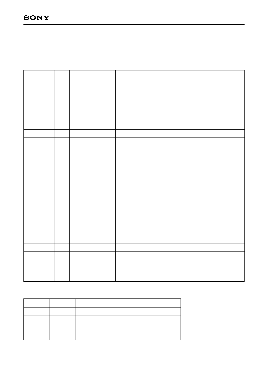
≠ 111 ≠
CXD1818R
CAT0 CMD5 CMD4 CMD3 CMD2 CMD1 CMD0
Description
CAT1
0
0
0
0
0
0
0
0
0
CAT1
0
0
0
0
CAT1
1
1
1
1
1
1
1
1
1
1
1
1
1
CAT1
1
1
1
1
1
0
0
0
0
0
0
0
0
0
CAT0
1
1
1
1
CAT0
0
0
0
0
0
0
0
0
0
0
0
0
0
CAT0
1
1
1
1
1
0
0
0
0
0
0
0
0
0
CMD5
0
0
0
0
BUF
0
0
0
0
0
CMD5
0
0
0
0
0
0
0
0
0
0
0
0
0
0
CMD4
0
0
0
0
SUB
0
0
0
0
0
CMD4
0
0
0
0
0
0
0
0
0
0
0
0
1
1
CMD3
0
0
0
0
CMD3
0
0
0
0
0
0
0
0
1
1
1
1
1
CMD3
0
0
0
0
0
0
0
0
1
1
1
1
0
0
CMD2
0
0
0
0
CMD2
0
0
0
0
1
1
1
1
0
0
0
0
1
CMD2
0
0
0
0
1
0
0
1
0
0
1
1
0
0
CMD1
0
0
1
1
CMD1
0
0
1
1
0
0
1
1
0
0
1
1
0
CMD1
0
0
1
1
0
0
1
1
0
1
0
1
0
1
CMD0
0
1
0
1
CMD0
0
1
0
1
0
1
0
1
0
1
0
1
0
CMD0
0
1
0
1
0
NOP
CHIP Reset
Flush FIFO
Assert SCSI Control
Deasert SCSI Control
Assert SCSI Data
Deasert SCSI Data
Enable Selection
Disable Selection
Description
Reselect and Send Message (s)
Initiate SCAM
Reselect, Send Message (s) and Receive Data
Reselect, Send Message (s) and Send Data
Description
Receive Data
Send Data
Reserved
Reserved
Reseive Command
Send Status
Receive Message
Send Message
Disconnect
Send Message (s) and Disconnect
Terminate I/O and bus free
Terminate I/O and link
Receive Command Sequence
Description
Stream Abort
Stream and Stop
Stream and Bus Free
Stream and Link
Stream Pause
Either "1" or "0" can be written. However, if the BUF bit is "1", "0" must be written for the SUB bit.
States which allow commands to be executed are limited by category.
CAT1
0
0
1
1
0
1
0
1
Can be executed in all states
Can be executed only in the Disconnect status
Can be executed only during the target mode
Stream commands
CAT0
Description
[4] Appendix B
4-1. Summary of SCSI Controller Block Commands
CXD1818R/SCSI2 core block command set
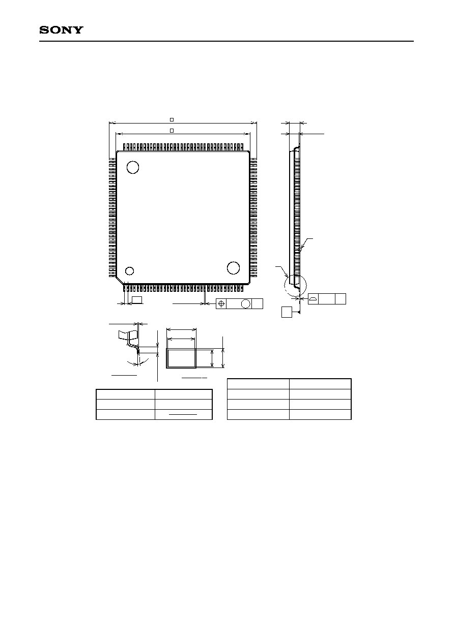
≠ 112 ≠
CXD1818R
Package Outline
Unit: mm
SONY CODE
EIAJ CODE
JEDEC CODE
PACKAGE STRUCTURE
PACKAGE MATERIAL
LEAD TREATMENT
LEAD MATERIAL
PACKAGE WEIGHT
EPOXY RESIN
SOLDER PLATING
42 / COPPER ALLOY
LQFP-144P-L01
LQFP144-P-2020-A
1.3 g
144PIN LQFP (PLASTIC)
0.1 ± 0.05
(21.0)
0.5 ±
0.15
0∞ to 10∞
(0.125)
0.145 ±
0.03
0.22 ± 0.05
(0.2)
DETAIL A
DETAIL B
1
36
37
72
73
108
109
144
0.22 ± 0.05
0.5
M
0.08
1.7 MAX
1.4 ± 0.1
A
B
0.1
S
S
22.0 ± 0.2
20.0 ± 0.1
S